Embed Size (px)
Citation preview
Power Amplifier Efficiency2 day Master Class
Rick Campbell PhDPortland State University
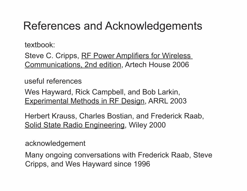
References and Acknowledgements
Steve C. Cripps, RF Power Amplifiers for Wireless Communications, 2nd edition, Artech House 2006
Many ongoing conversations with Frederick Raab, Steve Cripps, and Wes Hayward since 1996
Wes Hayward, Rick Campbell, and Bob Larkin, Experimental Methods in RF Design, ARRL 2003
Herbert Krauss, Charles Bostian, and Frederick Raab, Solid State Radio Engineering, Wiley 2000
textbook:
useful references
acknowledgement
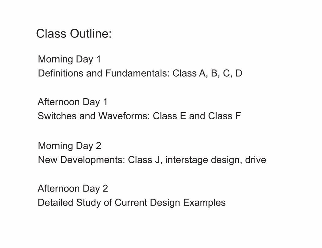
Class Outline:
Definitions and Fundamentals: Class A, B, C, DMorning Day 1
Switches and Waveforms: Class E and Class FAfternoon Day 1
New Developments: Class J, interstage design, drive Morning Day 2
Detailed Study of Current Design ExamplesAfternoon Day 2
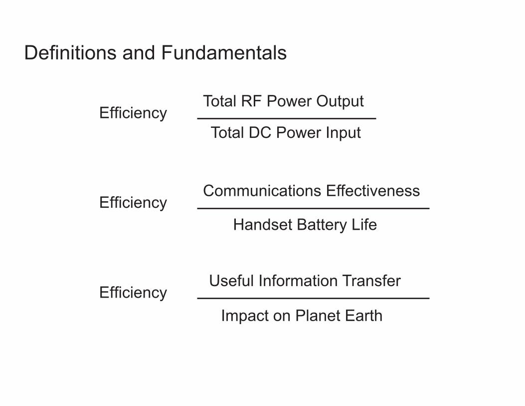
Definitions and Fundamentals
Total RF Power OutputEfficiency
Total DC Power Input
Communications EffectivenessEfficiency
Handset Battery Life
Useful Information TransferEfficiency
Impact on Planet Earth
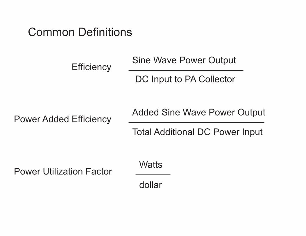
Common Definitions
Sine Wave Power OutputEfficiency
DC Input to PA Collector
Added Sine Wave Power OutputPower Added Efficiency
Total Additional DC Power Input
WattsPower Utilization Factor
dollar
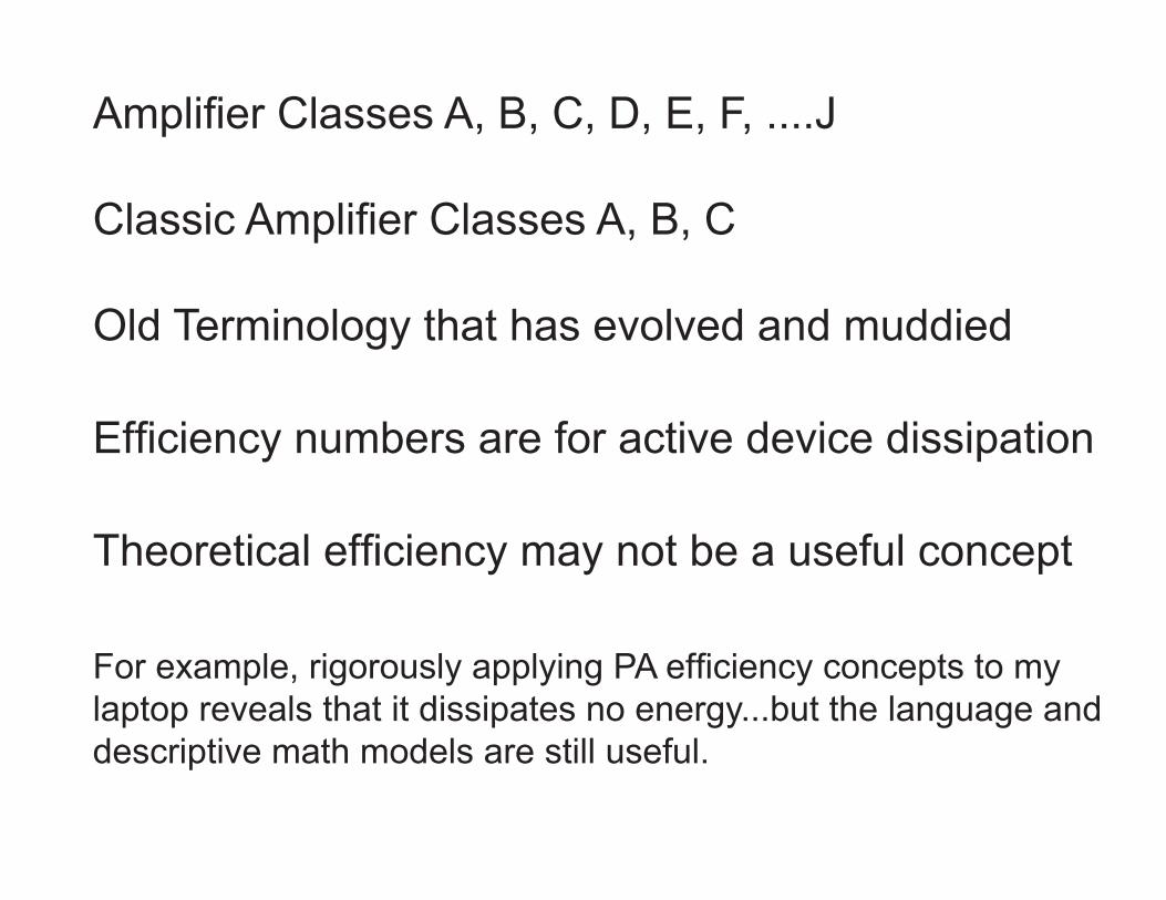
Amplifier Classes A, B, C, D, E, F, ....J
Classic Amplifier Classes A, B, C
Old Terminology that has evolved and muddied
Efficiency numbers are for active device dissipation
Theoretical efficiency may not be a useful concept
For example, rigorously applying PA efficiency concepts to my laptop reveals that it dissipates no energy...but the language and descriptive math models are still useful.
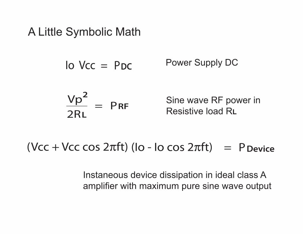
A Little Symbolic Math
Power Supply DCVccIo PDC=
Vp2R
P=L
2RF
P= Device
Sine wave RF power in Resistive load RL
Instaneous device dissipation in ideal class A amplifier with maximum pure sine wave output
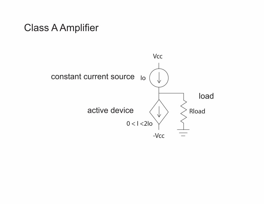
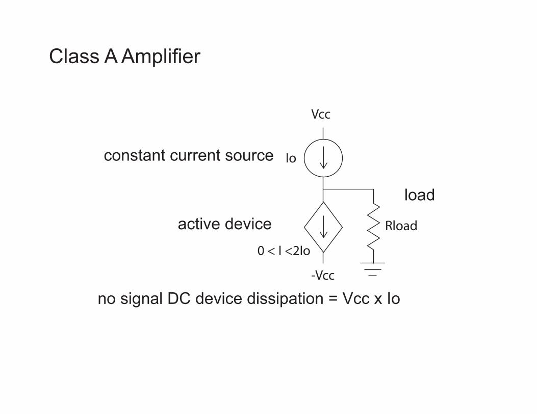
Class A Amplifier
Rload
Vcc
-Vcc
Io
0 < I <2Io
constant current source
active device
load
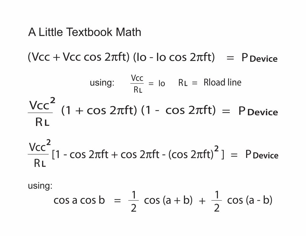
A Little Textbook Math
using:
P= Device
VccR
Io=L
RL = Rload line
VccR L
2P= Device
2VccR L
2P= Device
cos a cos b = cos (a + b)12
cos (a - b)12
+using:
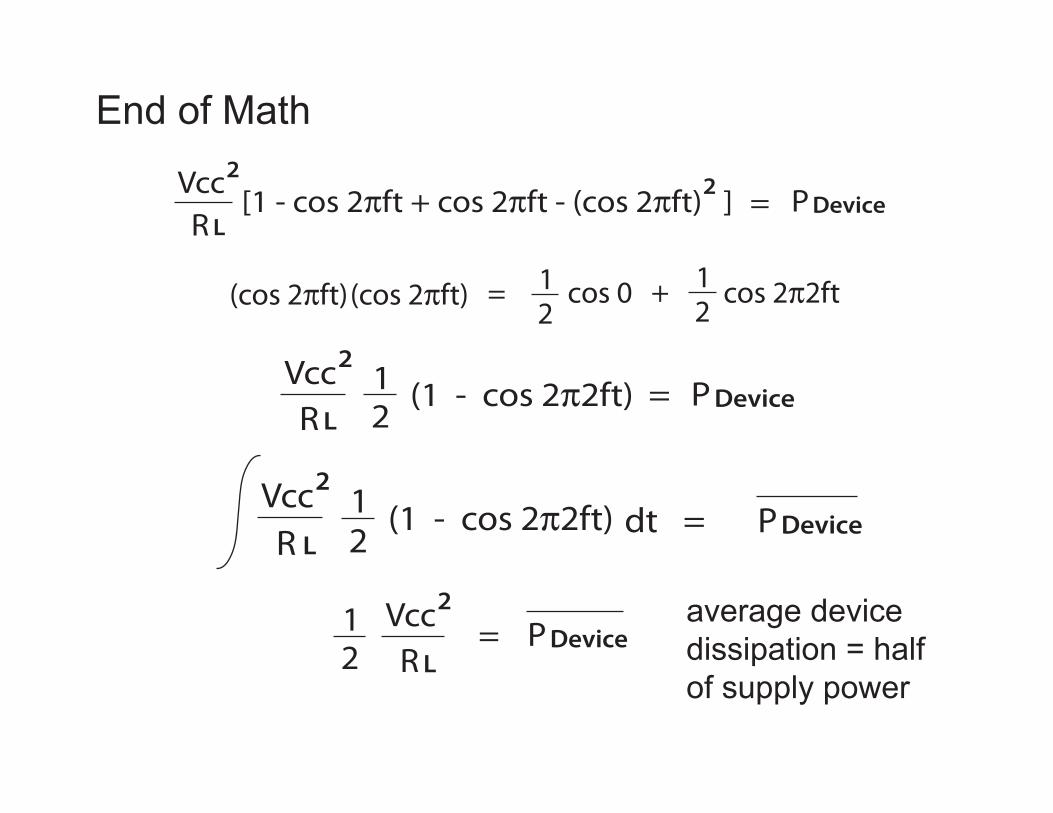
cos 0 = +12
12
2VccR L
2P= Device
VccR L
2P= Device
12
VccR L
2
P= Device12 dt
VccR L
212
PDevice=
End of Math
average device dissipation = half of supply power
Class A Amplifier
Rload
Vcc
-Vcc
Io
0 < I <2Io
constant current source
active device
load
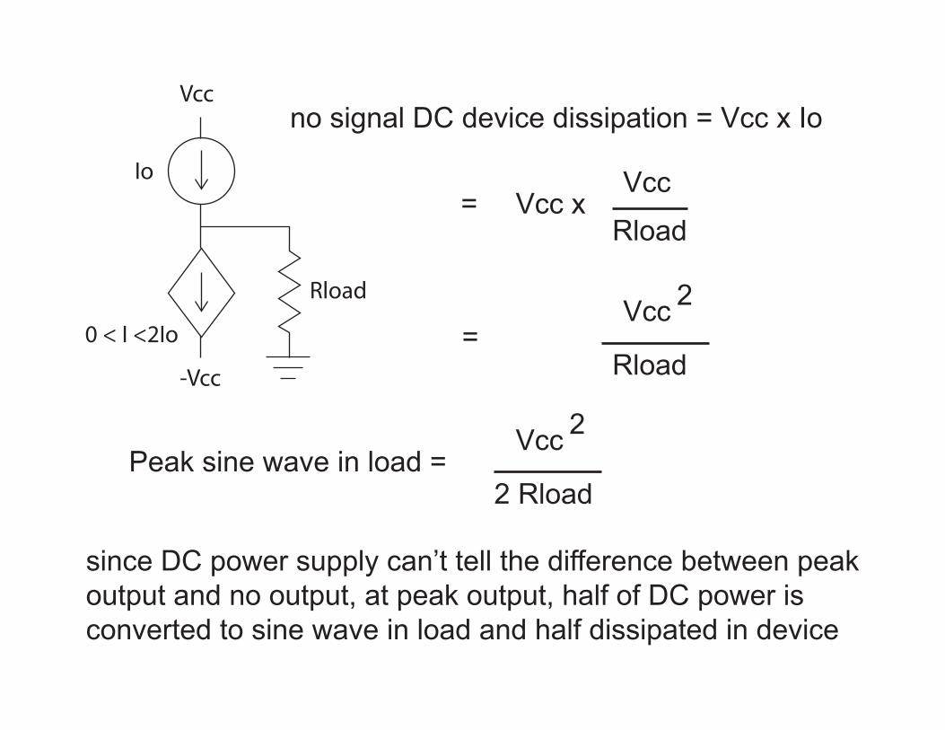
no signal DC device dissipation = Vcc x Io
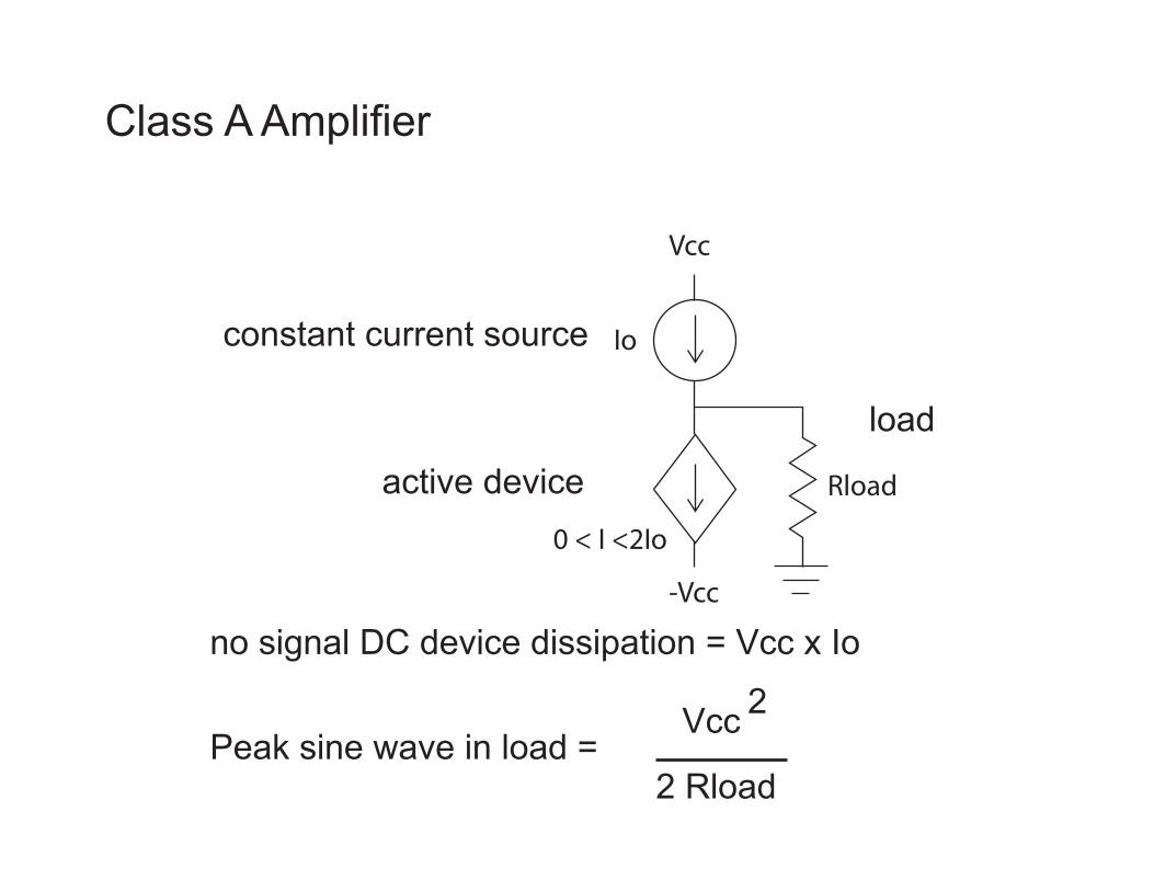
Class A Amplifier
Rload
Vcc
-Vcc
Io
0 < I <2Io
constant current source
active device
load
no signal DC device dissipation = Vcc x Io
Peak sine wave in load =Vcc 2
2 Rload
Rload
Vcc
-Vcc
Io
0 < I <2Io
no signal DC device dissipation = Vcc x Io
Peak sine wave in load =Vcc 2
2 Rload
Vcc xVcc
Rload=
Vcc 2
Rload=
since DC power supply can’t tell the difference between peak output and no output, at peak output, half of DC power is converted to sine wave in load and half dissipated in device
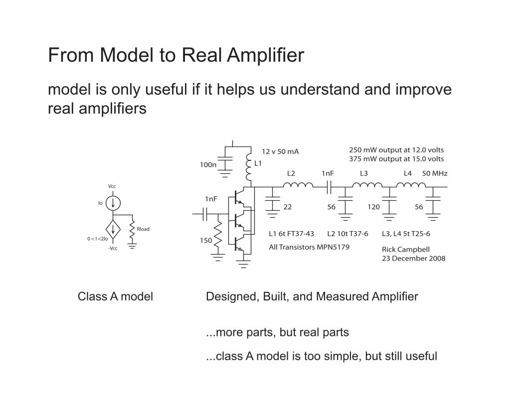
Rick Campbell23 December 2008
All Transistors MPN5179
100n
L1 6t FT37-43
12 v 50 mA 250 mW output at 12.0 volts375 mW output at 15.0 voltsL1
56 1201nF
1nF
56
150
22
L2 L3 L4
L2 10t T37-6 L3, L4 5t T25-6
50 MHz
Rload
Vcc
-Vcc
Io
0 < I <2Io
From Model to Real Amplifiermodel is only useful if it helps us understand and improve real amplifiers
Class A model Designed, Built, and Measured Amplifier
...more parts, but real parts
...class A model is too simple, but still useful
Vcc
Big L
Big C
Rload
Vc
Io
Vcc+ -
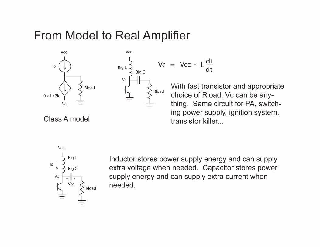
Vcc
Big L
Big C
Rload
Vc
Io
Vcc+ -
Rload
Vcc
-Vcc
Io
0 < I <2Io
Vcc
Big LBig C
Rload
Vc
Vc L didt
Vcc -=
With fast transistor and appropriate choice of Rload, Vc can be any-thing. Same circuit for PA, switch-ing power supply, ignition system, transistor killer...
From Model to Real Amplifier
Class A model
Inductor stores power supply energy and can supply extra voltage when needed. Capacitor stores power supply energy and can supply extra current when needed.
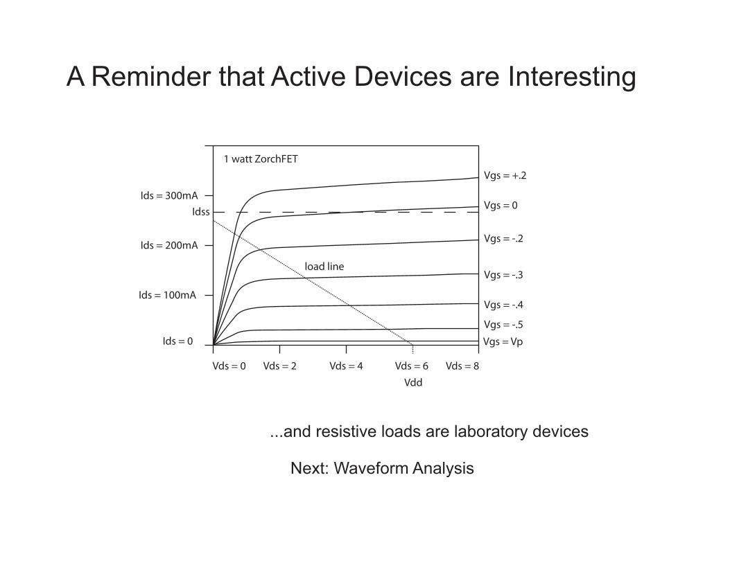
A Reminder that Active Devices are Interesting
Vgs = Vp
Vgs = 0
Vgs = -.2
Vgs = -.3
Vgs = -.4
Vgs = +.2
Vgs = -.5
Vds = 0 Vds = 8Vds = 2 Vds = 4 Vds = 6
Ids = 0
Idss
Ids = 100mA
Ids = 200mA
Ids = 300mA
Vdd
1 watt ZorchFET
load line
...and resistive loads are laboratory devices
Next: Waveform Analysis
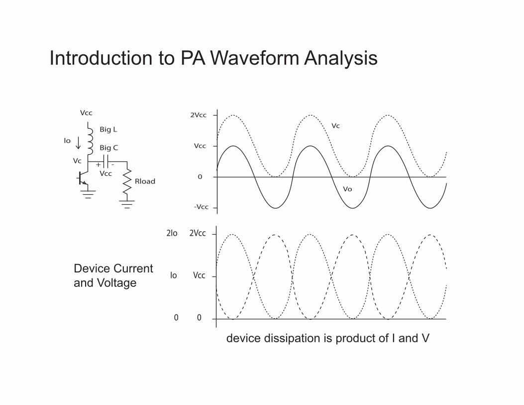
Introduction to PA Waveform Analysis
Device Current and Voltage
Vcc
Big L
Big C
Rload
Vc
Io
Vcc+ -
Vcc
-Vcc
2Vcc
0
Vc
Vo
Vcc
2Vcc
0
Io
2Io
0
device dissipation is product of I and V
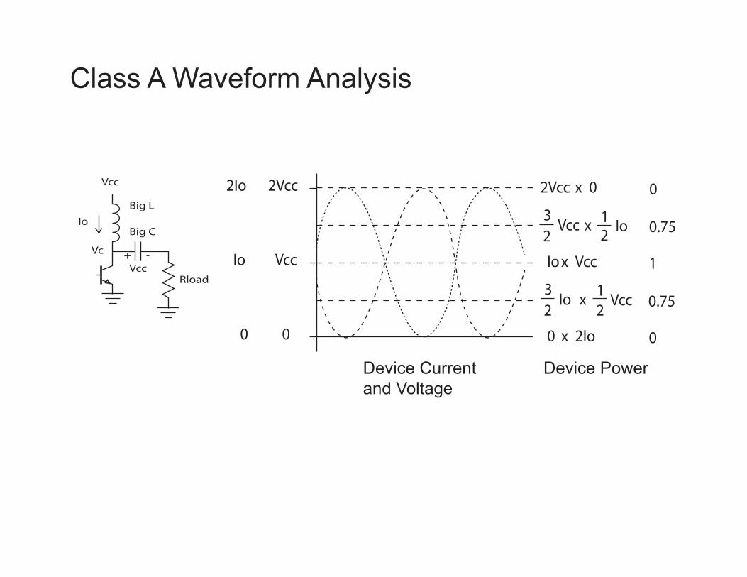
Class A Waveform Analysis
Device Current and Voltage
Vcc
Big L
Big C
Rload
Vc
Io
Vcc+ - Vcc
2Vcc
0
Io
2Io
0
VccIo x
0 2Iox
2Vcc x 0
32
Vcc 12
x Io
32
Vcc12
xIo
1
0
0
0.75
0.75
Device Power

Class A Waveform Analysis
Device Current and Voltage
Vcc
Big L
Big C
Rload
Vc
Io
Vcc+ -
sketch of instaneous device dissipation
note slightly real waveforms
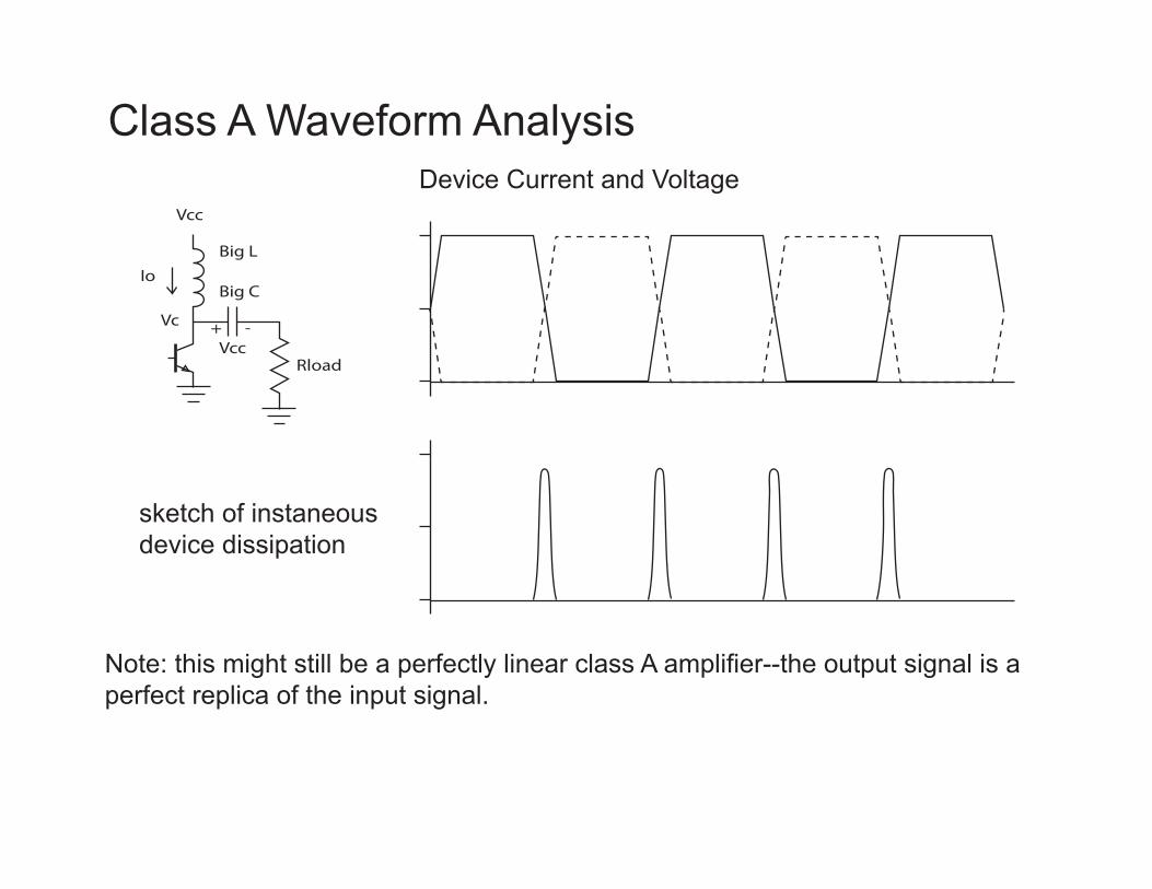
Class A Waveform Analysis
Device Current and VoltageVcc
Big L
Big C
Rload
Vc
Io
Vcc+ -
sketch of instaneous device dissipation
textbook waveforms
Average
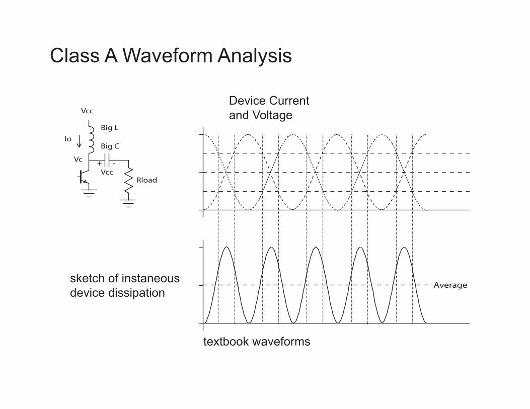
Class A Waveform AnalysisDevice Current and Voltage
Vcc
Big L
Big C
Rload
Vc
Io
Vcc+ -
sketch of instaneous device dissipation
Note: this might still be a perfectly linear class A amplifier--the output signal is a perfect replica of the input signal.
Class A Efficiency Review:
slight deviation from textbook waveform has big impact on device dissipation
textbook waveforms only appear in textbooks
waveform engineering is our primary tool to reduce device dissipation--even at frequencies where we can’t observe waveforms
Next: an alphabetical listing of amplifier classes
“The efficiency of a Class A amplifier” is not a number at the end of several pages of arcane math in a textbook


![A High Efficiency, Linear RF Power Amplifier With a Power ...users.ece.gatech.edu/rincon/publicat/jrnls/mtts03_pa_dyn.pdfDoherty amplifier for extended power range [4] has been demonstrated](https://img.pdfslide.net/doc/110x75/61489f672918e2056c22cec3/a-high-efficiency-linear-rf-power-amplifier-with-a-power-usersece-doherty.jpg)