Embed Size (px)
Citation preview
Power Charger Calibration Platform Application Note
AN0516E V1.00 1 / 12 March 25, 2019
Power Charger Calibration Platform Application Note
D/N:AN0516E
Overview
In the charger application area such as for electric bicycles and electric tools etc.
manufacturers often have to make adjustments to the products before leaving the factory
to ensure that the charger output voltage and current values are within specifications. The
traditional way of doing this is by using calibration fixtures which use fixed value or
variable resistors to determine the required resistance value. This method, in addition to
the labour costs also results in increased production times which have a major influence
on the product overall costs.
The HT45F5Q-2 charger ASSP MCU, which includes a fully integrated battery charger
module and EEPROM, can be used together with an automatic calibration fixture to
correct the charger output voltage and current values, whose parameters can then be
stored in the device’s internal EEPROM. This application note will explain how to
automatically correct the HOLTEK Charger ASSP MCU, such as the HT45F5Q-2, using
such a calibration fixture. A suitable calibration fixture can be designed in consultation
with this application note.
Functional Description
Charger Adjustment Reasons
During charger volume production, the actual output voltage and currents produced may
result in the charger being out of spec due to the product components tolerances (R2, R5
and R6 in the figure below) as well as other reasons.
Charger Principles
The HOLTEK charger ASSP MCU has a fully integrated battery charger module. The
example here uses the HT45F5Q-2 as an example. The internal DAC1 output is
compared with the voltage divider output, or the internal DAC0 is compared with the R2
current signal. The internal OPA outputs will switch the opto-coupler which in turn will

Power Charger Calibration Platform Application Note
AN0516E V1.00 2 / 12 March 25, 2019
change the Current Mode PWM IC output. In this way the required constant voltage or
constant current can be obtained. When the charger is powered on, the MCU will first
check whether it is connected to the calibration fixture through a 1-Wire communication
method to confirm whether it should enter the calibration mode. If the connection is
successful, the calibration will start and the correction value will be stored in the EEPROM.
Then when the charger is powered up each time, the MCU will load the EEPROM
updated calibration values.
Fig 1. HT45F5Q-2 Charger Application Circuit Diagram
Calibration Fixture Hardware Description Holtek charger calibration fixture - uses the HT66F2390 as an example.
1. AC/DC power supply circuit: AC 110V to DC 12V and 5V for use by the calibration
fixture, controls relay (K1) output to the charger AC power supply.
2. ADC reference voltage circuit: The external TL431 (D5) is used as the MCU A/D
reference voltage (VREF), with a variable resistor (VR2) added. Users can manually
adjust the ADC reference voltage by 4.0V to reduce the error.
3. Charger voltage detection circuit: In the Normal Mode, this will detect the voltage of the
charger and allow the LCM to display the voltage value. In the Test Mode, the voltage is
applied to B+/B-, and allows the LCM to display the voltage value. Manually adjust the
detection voltage using the variable resistor VR1 to ensure the measurement accuracy
of the charger voltage.
4. Charger current detection circuit: Use the current sense IC (U1) to measure current and
output voltage value to the MCU A/D.
5. Level Shift control circuit: The 5V signal is used to control the 12V relays (K1~K3)
through the voltage converter IC (U4).
6. Load switching circuit: Use ceramic resistors (R1, R2) for the charger load.
7. Charger connection circuit: The charger's AC power input is provided by the calibration
fixture (AC Output). The charger's DC power output is detected by the calibration fixture
(DC IN). The charger's TRx and the calibration fixture communicate using single-wire
communication.
U2 PC817
R10
D2
Battery
R2
Rectifier/Filter/Regulator
Q1
Current Mode PWM IC
R5
R6
R7
AC DC
5V LDO
C5
5V
D1
B+
5VR3
C8
5V
B+
AC_N
AC_L
C7
R4 C9
R8 C10
R9 C11
VDD
VSS
OPA2P
OPA0N
OPA1NOPAE
C2
DAC1 12Bit
DAC0 8Bit
ADC
OPA0
OPA1
OPA2
9R
R
U1 HT45F5Q-2
C1
C3
R1
C6C4
PB5
AC OutputAC_N
AC_L
B+B-
TRx1-Wire
DC IN

Power Charger Calibration Platform Application Note
AN0516E V1.00 3 / 12 March 25, 2019
Since the output voltage of the charger is charging C1, B+ and B- are equal to the high voltage
potential. If there is no Zener D4 voltage regulation to 5.1V and an R3 current limit, the high
voltage potential will be directly injected into the MCU A/D pin which will cause damage.
Calibration Fixture Circuit Diagram
Calibration Fixture and Charger Connection Instructions
During calibration, the charger needs to be connected to the calibration fixture using the
communication pins (TRx and GND), the AC input interface and the DC output interface
(B+, B-). This is shown in the accompanying diagram. The AC main power supply is
provided by the calibration fixture. In actual production, the contacts D, E and F can be
used to allow customers to design their preferred connection method.
Charger Calibration Fixture A: DC Output B+, B- ⇄ D: DC Input B+, B- B: Signal TRx, GND ⇄ E: Signal 1-Wire, GND C: AC Input ⇄ F: AC Output
Connection Description
Charger and Calibration Fixture Wiring Diagram

Power Charger Calibration Platform Application Note
AN0516E V1.00 4 / 12 March 25, 2019
Software Description
Users will have different requirements for the calibration protocol. The following is only a
conceptual architecture but users can design the protocol format according to their own
requirements. The following describes the software flow of the calibration fixture and the
charger.
Charger Fixture Single Line Communication Protocol Host: Calibration Fixture
Slave: Charger
Single-line communication definition: 1-bit total time of 1ms
Data 1: 700µs high-level, 300µs low-level
Data 0: 300µs high-level, 700µs low-level
Communication format: Instructio
n 01H 02H 03H 04H 05H 06H 07H 55H
Function Confirm Connectio
n
Start Increment
Power
Decrement Power
Confirm
Power
Adjustment Failed
Complete
Clear EEPRO
M
Communication Timing Diagram
Normal Communication
D7 D6 D5 D4 D3 D2 D1 D0 D7 D6 D5 D4 D3 D2 D1 D0
18ms Master Transmit Instruction 18ms Slave Return Instruction
Bus Master Signal Slave Signal First the host sends a start signal which is to pull down the bus for 18ms, after
which it sends the command
After the slave detects a start signal it starts receiving commands
After the host sends the command, it will change into a receiver state. If the slave
receives the correct command, it will send a start signal first and then reply to the
same host command after which the communication ends
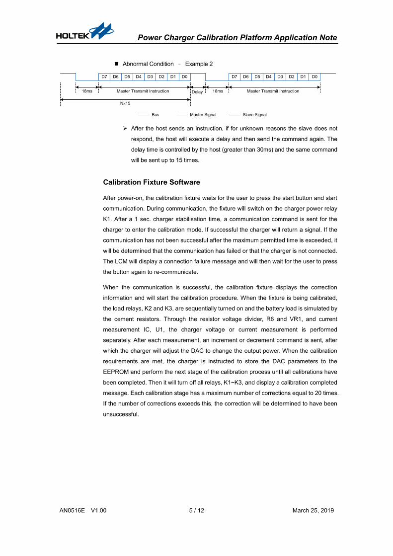
Abnormal Condition – Example 1
D7 D6 D5 D4 D3 D2 D1 D0
18ms Master Transmit Erroneous Instruction
Bus Master Signal Slave Signal If the host send out an erroneous instruction, the slave will not respond
Power Charger Calibration Platform Application Note
AN0516E V1.00 5 / 12 March 25, 2019
Abnormal Condition – Example 2
D7 D6 D5 D4 D3 D2 D1 D0 D7 D6 D5 D4 D3 D2 D1 D0
18ms Master Transmit Instruction 18ms Master Transmit Instruction
Bus Master Signal Slave Signal
Delay
N×15
After the host sends an instruction, if for unknown reasons the slave does not
respond, the host will execute a delay and then send the command again. The
delay time is controlled by the host (greater than 30ms) and the same command
will be sent up to 15 times.
Calibration Fixture Software
After power-on, the calibration fixture waits for the user to press the start button and start
communication. During communication, the fixture will switch on the charger power relay
K1. After a 1 sec. charger stabilisation time, a communication command is sent for the
charger to enter the calibration mode. If successful the charger will return a signal. If the
communication has not been successful after the maximum permitted time is exceeded, it
will be determined that the communication has failed or that the charger is not connected.
The LCM will display a connection failure message and will then wait for the user to press
the button again to re-communicate.
When the communication is successful, the calibration fixture displays the correction
information and will start the calibration procedure. When the fixture is being calibrated,
the load relays, K2 and K3, are sequentially turned on and the battery load is simulated by
the cement resistors. Through the resistor voltage divider, R6 and VR1, and current
measurement IC, U1, the charger voltage or current measurement is performed
separately. After each measurement, an increment or decrement command is sent, after
which the charger will adjust the DAC to change the output power. When the calibration
requirements are met, the charger is instructed to store the DAC parameters to the
EEPROM and perform the next stage of the calibration process until all calibrations have
been completed. Then it will turn off all relays, K1~K3, and display a calibration completed
message. Each calibration stage has a maximum number of corrections equal to 20 times.
If the number of corrections exceeds this, the correction will be determined to have been
unsuccessful.

Power Charger Calibration Platform Application Note
AN0516E V1.00 6 / 12 March 25, 2019
Charger Software
For three seconds after power-on, the charger will continuously detect whether the
calibration fixture requires calibration. If a communication command from the calibration
fixture is not received within this time, it will enter the charger mode. If a communication
command is received and communication command successfully returned, the calibration
program will be started.
At the beginning of the calibration, the charger adjusts the integrated DAC (increment or
decrement) according to the calibration fixture command, thereby adjusting the CV and
CC values until the calibration is complete after which the DAC values are written into the
EEPROM to complete the calibration program. Then wait for the charger to power up
again but this time do not enter the calibration program. The charger will read the
correction values in the EEPROM to update the DAC, and then start executing the normal
charger program. Each calibration stage has a maximum number of corrections equal to
20 times. If the number of corrections exceeds this, the correction will be considered to be
unsuccessful and no adjustment will take place until another correction command is
received.
Power Charger Calibration Platform Application Note
AN0516E V1.00 7 / 12 March 25, 2019
Start
Charge Flowchart
Calibration Fixture Flowchart
Initialise
Receive connection instruction
Received connection instruction?
Received erroneous
instruction?
Exceeded time?
FV voltageDAC adjustment
complete?
CV voltageDAC adjustment
conplete?
TC currentDAC adjustment
complete?
CC currentDAC adjustment
complete?
Write calibration values into EEPROM
End
Keep EEPROM default values
Start
Initialise
Turn off power relayCharger transmits
connection instruction
Return instruction received? Exceeded time?
Select calibration charger type
Is start key pressed?
Start corresponding charger mode relays
Inform charger to adjust DAC
Calibration complete?
Exceeded max. number of
adjustment times?
Transmit write to EEPROM instruction and display success
Transmit fail instruction and LCM
displays fail
End
Switch off all relaysCalibration cimplete
Step 1
Step 2
Step 3, Step4
Y
N
N
Y
Y
Y
Y
Y
Y
Y
Y
Y Y
Y
N
N
N
N
N
N
N
N
N
N
Charger calibration flow complete
Charger operating mode
Step 5, Step6
Calibration Fixture Step Description
Step 1: After the fixture is powered on, select the charger type to be calibrated,
press the start button, turn on the charger power relay (AC Output), and send a
connection command.
Step 2: Wait for a return command and check that the time has not been exceeded
and confirm that the charger has entered the calibration mode. If communication
cannot be established with the calibration fixture then the calibration process will
stop.

Power Charger Calibration Platform Application Note
AN0516E V1.00 8 / 12 March 25, 2019
Step 3: Connect the required load in the charging mode, measure the charger
output status and the charger to adjust the DAC mode to fine tune the output
voltage or current.
Step 4: When the charger output voltage or current meets requirements, the charger
is instructed to save the correction value to the EEPROM and displays a calibration
success. If the calibration has not completed within the maximum correction time,
the charger is instructed to skip this calibration item and display a calibration failure.
Step 5: Repeat steps 3 and 4 until all voltage and current calibration items have
been corrected.
Charger Step Description
Step 1: Initialise the settings after the charger is powered on and receive the
connection command.
Step 2: The charger establishes communication with the calibration fixture and
enters the calibration mode. If communication cannot be established with the
calibration fixture, the default value in the EEPROM will be kept and returned to the
charger operating mode.
Step 3: Start the calibration process.
Step 4: Send a correction command according to the calibration fixture to adjust the
DAC mode and fine tune the output voltage or current.
Step 5: Send the completion command according to the calibration fixture to
complete the point correction at this stage. If successful, the DAC value is stored in
the EEPROM. If it fails, the point correction is skipped and the next calibration item
will be executed.
Step 6: Repeat steps 4 and 5 until the calibration fixture sends a calibration end
command to end the calibration process.
Select Type Display Calibration Display
Calibration Complete Display Connection Failed Display

Power Charger Calibration Platform Application Note
AN0516E V1.00 9 / 12 March 25, 2019
Calibration fixtures are preset to four calibration points: floating voltage charging,
constant voltage charging, trickle current charging and constant current charging.
Taking a 48V lead-acid battery as an example, note the following process:
Floating voltage charging (FV): Constant voltage charging, used for self-discharge
maintenance after the battery has been fully charged, and can also be trickle
charged.
Constant voltage charging (CV): Constant voltage charging, supplementing the part
that has not been fully charged after constant current charging.
Trickle charge (TC): Constant small current charging for when the battery has been
deep-discharged, a small current can re-activate the battery.
Constant current charging (CC): Constant current charging to prevent rapid battery
temperature rise which can reduce battery life and charging efficiency
The correction fixture voltage and current AD value calculation formula is as follows:
AD voltage value calculation: ADVBAT = 4096VREF
× �VBAT × VR1R6+VR1
�
Example: 59V AD voltage value: 𝐴𝐴𝐴𝐴𝑉𝑉𝑉𝑉𝑉𝑉𝑉𝑉 = 40964
× �59𝑉𝑉 × 1𝑘𝑘20𝑘𝑘+1𝑘𝑘
� = 2876 =𝐵𝐵3𝐶𝐶 𝐻𝐻
Note:Demo Board R6=20k , VR1=1kk, VREF=4.0V、VBAT= charging voltage 59V
AD current value calculation: 𝐴𝐴𝐴𝐴𝐼𝐼𝑉𝑉𝑉𝑉𝑉𝑉 = 4096𝑉𝑉𝑅𝑅𝑅𝑅𝑅𝑅
× (0.185 × 𝐼𝐼𝑉𝑉𝑉𝑉𝑉𝑉)
Example: 0.2A AD current value: 𝐴𝐴𝐴𝐴𝐼𝐼𝑉𝑉𝑉𝑉𝑉𝑉 = 40964
× (0.185 × 0.2𝐴𝐴) = 37 = 25 𝐻𝐻
Note:Demo Board R6=20k , VR1=1kk, VREF=4.0V, IBAT= Charging Current
0.2A
Correct the calibration fixture data, register setup values are shown below:
Calibration Steps Setup Values Decimal 16-bit hex
Floating Voltage Charging (FV)=55V 2681 0A79H
Constant Voltage Charging (CV)=59V 2876 0B3CH
Trickle Current Charging (TC)=0.2A 37 0025H
Constant Current Charging (CC)=2.0A 378 017AH
Parameter Calculation The charger output voltage and current are measured and assessed by the MCU ADC on
the calibration fixture. The output voltage signal is read from the 20kΩ and 1kΩ resistors
voltage divider. The preset resistors are R6 and VR1, which are used to convert the
voltage signal. The formula is:
𝐴𝐴𝐴𝐴𝑉𝑉𝑉𝑉𝑉𝑉𝑉𝑉 =4096𝑉𝑉𝑅𝑅𝑅𝑅𝑅𝑅
× �𝑉𝑉𝑉𝑉𝑉𝑉𝑉𝑉 ×𝑉𝑉𝑉𝑉1
𝑉𝑉6 + 𝑉𝑉𝑉𝑉1�

Power Charger Calibration Platform Application Note
AN0516E V1.00 10 / 12 March 25, 2019
The charger output current is measured by the current sensing IC (ACS712ELCTR-05B-T)
and supports a maximum current measurement of 5A, the detailed specifications are
shown below. The current conversion voltage formula is
𝐴𝐴𝐴𝐴𝐼𝐼𝑉𝑉𝑉𝑉𝑉𝑉 = 4096𝑉𝑉𝑅𝑅𝑅𝑅𝑅𝑅
× (0.185 × 𝐼𝐼𝑉𝑉𝑉𝑉𝑉𝑉) (as shown in the following red frame)
Using the HT66F2390 12-Bit A/D with a reference voltage of 4.00V gives the following
resolution:
𝐼𝐼𝑅𝑅𝑅𝑅𝑅𝑅𝑅𝑅𝑅𝑅𝑅𝑅𝑅𝑅𝑅𝑅𝑅𝑅𝑅𝑅 =4
40960.185 ≅ 5.3𝑚𝑚𝐴𝐴
ACS712ELCTR-05B-T Specification Table
Correction Error Calculation
The corrected ADC value is compared with the tolerance maximum and minimum values.
The error is corrected to achieve an accurate measurement of to achieve with the
current sensing IC . However, the correction is still limited by each DAC. If the
corresponding voltage or current has exceeded the specification, the calibration fixture
will not have met the calibration requirements even if the measurement accuracy is
accurate.
ADC value is within tolerance Each DAC step is too large for calibration
Using FV=55V as an example, the AD conversion value is 2655~2709 so a value
between this can be taken
Parameter Theoretical Value R6 VR1 Permitted
Error ADC Conversion
Value
FV 55V 20k 1kk +1% 2709 -1% 2655
Using CC=2A as an example, the AD conversion value is 360~398 so a value between
this can be taken
Parameter Theoretical Value Permitted Error ADC Conversion Value
CC 2A +5% 398 -5% 360
ADC value ADC value
Power Charger Calibration Platform Application Note
AN0516E V1.00 11 / 12 March 25, 2019
Correction fixture load component selection
The calibration fixture uses cement resistors to simulate the battery load. The resistor
voltage is used to measure the charger output voltage, and a current sensing IC
measures the charger output current. The choice of cement resistance should pay
attention to the resistance and power ratings. For example, if the output voltage of the
charger is 60V and the output current is 2A, the resistance value should be 30Ω (R=V/I),
and the rated power must be 120W (P=I2 R). However, when taking into account the
loading time during the calibration process, the power should be multiplied by the ratio of
the use time. If the time ratio is 1/5, the resistance power can be reduced to about 24W.
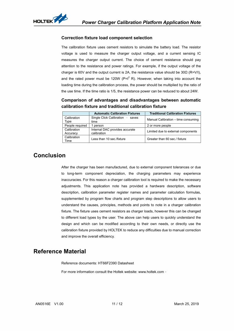
Comparison of advantages and disadvantages between automatic calibration fixture and traditional calibration fixture
Automatic Calibration Fixtures Traditional Calibration Fixtures Calibration Type
Single Click Calibration – saves time Manual Calibration – time consuming
People required 1 person 2 or more people Calibration Accuracy
Internal DAC provides accurate calibration Limited due to external components
Calibration Time Less than 10 sec./fixture Greater than 60 sec./ fixture
Conclusion
After the charger has been manufactured, due to external component tolerances or due
to long-term component depreciation, the charging parameters may experience
inaccuracies. For this reason a charger calibration tool is required to make the necessary
adjustments. This application note has provided a hardware description, software
description, calibration parameter register names and parameter calculation formulas,
supplemented by program flow charts and program step descriptions to allow users to
understand the causes, principles, methods and points to note in a charger calibration
fixture. The fixture uses cement resistors as charger loads, however this can be changed
to different load types by the user. The above can help users to quickly understand the
design and which can be modified according to their own needs, or directly use the
calibration fixture provided by HOLTEK to reduce any difficulties due to manual correction
and improve the overall efficiency.
Reference Material
Reference documents: HT66F2390 Datasheet
For more information consult the Holtek website: www.holtek.com。

Power Charger Calibration Platform Application Note
AN0516E V1.00 12 / 12 March 25, 2019
Version and Modification Information
Date Author Issue Release and Modification
2018.11.30 王駿維 First Version
Disclaimer
All information, trademarks, logos, graphics, videos, audio clips, links and other items
appearing on this website ('Information') are for reference only and is subject to change at
any time without prior notice and at the discretion of Holtek Semiconductor Inc.
(hereinafter 'Holtek', 'the company', 'us', 'we' or 'our'). Whilst Holtek endeavors to ensure
the accuracy of the Information on this website, no express or implied warranty is given
by Holtek to the accuracy of the Information. Holtek shall bear no responsibility for any
incorrectness or leakage.
Holtek shall not be liable for any damages (including but not limited to computer virus,
system problems or data loss) whatsoever arising in using or in connection with the use of
this website by any party. There may be links in this area, which allow you to visit the
websites of other companies. These websites are not controlled by Holtek. Holtek will
bear no responsibility and no guarantee to whatsoever Information displayed at such sites.
Hyperlinks to other websites are at your own risk.
Limitation of Liability In no event shall Holtek Limited be liable to any other party for any loss or damage
whatsoever or howsoever caused directly or indirectly in connection with your access to
or use of this website, the content thereon or any goods, materials or services.
Governing Law The Disclaimer contained in the website shall be governed by and interpreted in
accordance with the laws of the Republic of China. Users will submit to the non-exclusive
jurisdiction of the Republic of China courts.
Update of Disclaimer Holtek reserves the right to update the Disclaimer at any time with or without prior notice,
all changes are effective immediately upon posting to the website.