Embed Size (px)
Citation preview

8/7/2019 power electronics paper
http://slidepdf.com/reader/full/power-electronics-paper 1/13
66 IEEE TRANSACTIONS ON POWER ELECTRONICS, VOL. 26, NO. 1, JANUARY 2011
An Efficient High-Step-Up Interleaved DC–DCConverter With a Common Active Clamp
Suman Dwari, Student Member, IEEE , and Leila Parsa, Member, IEEE
Abstract—This paper presents a high-efficiency and high-step-up nonisolated interleaved dc–dc converter with a common active-clamp circuit. In the presented converter, the coupled-inductorboost converters areinterleaved. A boost converter is used to clampthe voltage stresses of all the switches in the interleaved converters,caused by the leakage inductances present in the practical coupledinductors, to a low voltage level. The leakage energies of the inter-leaved converters are collected in a clamp capacitor and recycled tothe output by the clamp boost converter. The proposed converterachieves high efficiency because of the recycling of the leakageenergies, reduction of the switch voltage stress, mitigation of theoutput diode’s reverse recovery problem, and interleaving of theconverters. Detailed analysis and design of the proposed converter
arecarriedout. A prototype of the proposed converter is developed,and its experimental results are presented for validation.
Index Terms—Active-clamp, boost converter, coupled-inductorboost converter, dc–dc power converter, high voltage gain,interleaving.
I. INTRODUCTION
IN MANY applications, high-efficiency, high-voltage step-
up dc–dc converters are required as an interface between the
available low voltage sources and the output loads, which are
operated at much higher voltages. Examples of such applications
are as follows. Different distributed energy storage components
such as batteries, fuel cells, and ultracapacitors are used in thepower trains of hybrid electric vehicles (HEV), electric vehicles
(EV), and fuel cell vehicles (FCV). In the present power train
architectures of these vehicles, the voltage levels of the energy
storage elements are usually low; whereas the motors of the
vehicles are driven at much higher voltages [1]–[4]. Next, the
telecom and the computer industry utilize the standard batteries,
with low voltage levels, as a back-up power source [5], [6].
In such applications, a front-end converter with dual inputs is
used. The dc–dc converter, used in this case, is required to
boost the low-input voltage of the batteries to the high voltage
of the dc bus. Another example is the automotive headlamps,
using the high-intensity discharge lamp ballasts [5], [7]. Thedc–dc converter, used in this application, is required to boost
the low voltage level of car battery to much higher voltage
Manuscript received November 19, 2009; revised February 12, 2010;accepted May 11, 2010. Date of current version December 27, 2010. Rec-ommended for publication by Associate Editor Y.-F. Liu.
The authors are with the Department of Electrical, Computer and SystemsEngineering, Rensselaer Polytechnic Institute, Troy, NY 12180 USA (e-mail:[email protected]; [email protected]).
Color versions of one or more of the figures in this paper are available onlineat http://ieeexplore.ieee.org.
Digital Object Identifier 10.1109/TPEL.2010.2051816
level during the start-up and normal operations. Finally, few
emerging applications, such as photovoltaic cells, also require
high-gain dc voltage conversion [8]. It can be noted that in all
these applications, the high-step-up dc–dc converters can be
nonisolated but they should operate at high efficiency while
taking high currents from low-voltage dc sources at their inputs.
In a conventional boost converter, the duty ratio increases
as the output to input voltage ratio increases. However, the
previously mentioned applications require high-voltage step-up
(step-up ratio 6 or more) and high-efficiency power conver-
sion. Therefore, the conventional boost converters will require
extreme duty ratios to meet the high-voltage step-up require-ments [9]–[11]. Under such conditions, it is a major challenge
to operate the boost converters at high efficiency [12]. This is be-
cause,with thehigh-output voltage, theboostswitch hasto block
a large voltage and hence the ON-state resistance, RD S -ON ,
which varies almost proportionally with the square of block-
ing voltage, will be very high. Furthermore, the low-level input
voltages cause large input currents to flow through the switches.
The extreme duty-cycle operation drives short-pulsed currents
with high amplitude to flow through the output diodes and the
capacitors; which cause severe diode reverse recovery prob-
lem and increases in the conduction losses. The high RD S -ON
of the switches, the increased conduction losses, and the se-vere reverse-recovery problem will degrade the efficiency and
limit the power level of the conventional boost converters [12].
Moreover, the parasitic ringing, present in the practical circuits,
induces additional voltage stresses and necessitates the use of
switches with higher blocking voltage ratings, which will lead
to more losses.
The coupled-inductor boost converter [see Fig. 1(a)] can be
a good solution to the previously discussed problems of the
conventional boost converter. This is because the turns ratio of
the primary inductor (L1 ) to the secondary inductor (L2 ) of
the coupled inductor can be effectively used to reduce the duty
ratio and the voltage stress of the switch [5], [16], [21]–[24].
Therefore, for high-voltage step-up applications, the coupled-
inductor boost converter can be more efficient than the conven-
tional boost converter. However, for high power applications,
handling of very large input currents from the low-input voltage
sources remains a practical issue. Various converter topologies
using magnetically coupled inductors are reported in the litera-
ture to reduce to the extreme duty ratio operation for nonisolated
high step-up applications [14]–[17]. But they are not suitable
for high current and high power applications, and moreover, the
circuits are complex to design and model. For high-input cur-
rent, it can be proposed to interleave the coupled-inductor boost
converters to process high power, and to achieve high efficiency
0885-8993/$26.00 © 2010 IEEE

8/7/2019 power electronics paper
http://slidepdf.com/reader/full/power-electronics-paper 2/13
DWARI AND PARSA: EFFICIENT HIGH-STEP-UP INTERLEAVED DC–DC CONVERTER WITH A COMMON ACTIVE CLAMP 67
Fig. 1. (a) Coupled-inductor boost converter and (b) interleaved coupled-inductor boost converter.
and high reliability with reduced size inductors and capaci-
tors [20]. Various advantages of interleaving are well reported
in the literature [10], [18], and [19]. The schematic diagram
of the proposed interleaved coupled-inductor boost converter isshown in Fig. 1(b).
An interleaved boost converter with three winding-based cou-
pled inductors is reported in [21] and [22]. This converter has
two interleaved phases, and the inductors of one interleaved
phase are coupled with the inductors of the other interleaved
phase. Therefore, with this converter the modular structure,
which is a key beneficial feature of the interleaved convert-
ers, cannot be realized. Furthermore, the maximum number of
interleaved phases is only two in this converter. The interleaved
converter, presented in this paper, is modular and can be de-
signed for any number of phases.
In a practical coupled inductor, there will be considerable
amount of leakage inductance present due to the nonideal cou-pling between the primary inductor (L1 ) and the secondary in-
ductor (L2 ) [see Fig. 2(a)]. The leakage inductance (Ll ) causes
high voltage stresses to the switches, large switching losses,
parasitic ringing, and severe electromagnetic interference prob-
lems, which degrade the converter performances [12] and [16].
Resistor–capacitor–diode (RCD)-based snubber circuits can be
used to mitigate the problem, but the losses in these circuits are
very high [13] and [17]. Active-clamp circuits can be used to
address this issue [17]. But these clamp circuits are complex
and costly. Moreover, the efficiency improvement in these cir-
cuits is limited by the high conduction loss in the active-clamp
switches [5], [13], and [18].
Fig. 2. (a) Nonidealcoupled-inductor boost converter withleakage inductanceand (b) coupled-inductor boost converter with capacitor and series diode-based
passive-clamp circuit [5].
A diode and capacitor-based passive-clamp circuit is pro-
posed in [5]. In this clamp circuit, the clamp capacitor (C c ) is
discharged to the output through the secondary side inductor
(L2 ) of the coupled-inductor boost converter [see Fig. 2(b)].
However, the clamp diode (Dc ), in this circuit, is in series with
the coupled inductor. Therefore, it’s not only the leakage in-
ductance current, but the total coupled-inductor current, which
flows through the clamp diode (Dc ). This causes large losses in
the clamp diode. The clamp diode needs to be rated for the entire
large power processed by the coupled-inductor boost converter.This can make the converter operation inefficient for the higher
power applications. Furthermore, in this clamp circuit, to take
the advantages of the reduced switch voltage stress feature of
the coupled-inductor boost converter, the clamp capacitor has to
be considerably large, capable of handling the high amount of
charge, and discharge currents of the converter. Also, this will
cause additional losses in the clamp capacitor. It can be noted
that, if any of the previously discussed clamp circuit is used
in the interleaved coupled-inductor boost converter; each of the
interleaved phases of the converter will require additional clamp
circuit components and control circuits (for active clamp). This
will increase the cost, size, and complexity.
A single active-clamp circuit can be proposed, in whichthe energy stored in leakage inductances of all the interleaved
coupled-inductor boost converters are gathered in a common
clamp capacitor [20]. In each of the interleaved units, a clamp
diode is connected from the common node of the coupled in-
ductors to the clamp capacitor for providing the discharge path
of the leakage energy. Therefore, only the leakage currents flow
through the clamp diodes; this makes the clamping operation
efficient. A simple boost converter is used to recycle the leak-
age energy, gathered in the clamp capacitor, to the output of
the interleaved converter. The boost converter is controlled to
keep the clamp-capacitor voltage to a low level, and hence, the
voltage stress on the switches is low. This allows the use of
8/7/2019 power electronics paper
http://slidepdf.com/reader/full/power-electronics-paper 3/13

8/7/2019 power electronics paper
http://slidepdf.com/reader/full/power-electronics-paper 4/13
DWARI AND PARSA: EFFICIENT HIGH-STEP-UP INTERLEAVED DC–DC CONVERTER WITH A COMMON ACTIVE CLAMP 69
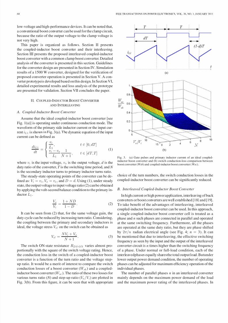
Fig. 4. (a) Three-phase interleaved converter with ideal coupled-inductorboost converters and (b) from top to bottom: gate pulses, primary inductorcurrents, and output capacitor charging current.
this paper, the output load is considered to be 1500 W. Further-
more, the maximum power rating of each interleaved phases is
considered to be 500 W. Therefore, the number of phases to
be interleaved for supplying the total output power is n = 3.
The input currents and the output currents of these interleavedphases are shown in Fig. 4(b). It can be noticed that the output
currents in the individual phases are discontinuous, and they are
phase shifted by 2π/3 radians. The summation of the output
currents of the interleaved converters (ioc ) charges the output
capacitor and provides the current required by the load. For a
fixed number of interleaved units, the ac component of this total
current, which charges the output capacitor, is mainly decided
by the operating duty cycle of the converter. It can be noted that
for three interleaved coupled-inductor boost converters (n = 3),
the output ripple is minimum when the duty cycle D = 0.33 or
D = 0.66 [12], [18]. As the input voltage is low, with lower duty
cycle D = 0.33, the input current peak and its rms value will
Fig. 5. (a) Parallel diode clamped coupled-inductor boost converter and(b) proposed interleaved coupled-inductor boost converter with single boostconverter clamp (for n = 3).
be larger. This will cause higher losses and require devices with
higher current rating. Therefore, the larger duty cycle D = 0.66
can be chosen for the nominal operation of the converter.
III. INTERLEAVED COUPLED-INDUCTOR CONVERTER
WITH A COMMON ACTIVE CLAMP
In the practical coupled inductors, due to the nonideal cou-
pling between the primary and the secondary windings, there
will be leakage inductances. The equivalent circuit diagram of
a practical converter with the leakage inductance is shown in
Fig. 2(a). This leakage inductancewill causehigh-voltage spikeswhen theswitch is turnedoff. This results in a high-voltagestress
across the switches and in ringing losses. It can be proposed to
clamp the switch voltage to the output voltage, using a parallel
diode [see Fig. 5((a)]. In this clamp circuit, the energy stored in
the leakage inductance is discharged directly to the output by the
parallel diode, and the switch voltage is clamped to the output
voltage. It can be seen that this converter avoids the disadvan-
tage of series conduction loss of the total power, but the switch
voltage stress becomes equal to the output voltage. So this con-
figuration does not take full advantages of the coupled-inductor
boost topology, and hence, it is not suitable for high-step-up
application where the output voltage level is high.

8/7/2019 power electronics paper
http://slidepdf.com/reader/full/power-electronics-paper 5/13
70 IEEE TRANSACTIONS ON POWER ELECTRONICS, VOL. 26, NO. 1, JANUARY 2011
To lower the voltage stress on the switches close to the level of
the voltage stresspresent in an ideal coupled-inductor boost con-
verter,a common active-clamp circuit based on a boost converter
can be proposed, as shown in Fig. 5(b). In the proposed active-
clamp circuit, in each phase, a clamp-diode (Dc1 , Dc2 , . . . Dcn )
is connected to the common node of the primary inductor, the
secondary inductor, and the switch of an interleaved coupled-
inductor boost converter. The cathode terminals of all the clamp
diodes are connected to a clamp capacitor C c . The energies
stored in the leakage inductors of the interleaved phases are
discharged through the clamp diodes and gathered in the clamp
capacitor C c . Furthermore, the boost converter is used to trans-
fer the stored energy in the clamp capacitor to the output of
the interleaved converters, while maintaining the voltage level
of the clamp capacitor to a lower level [see Fig. 5(b)]. The
voltage stress on the switches (S 1 , S 2 , . . . S n ) is decided by
this clamp-capacitor voltage. It can be suggested that any other
converter topology, which can perform similar boost operation
while maintaining the voltage level of the clamp capacitor can
be also used for the active-clamp operation.
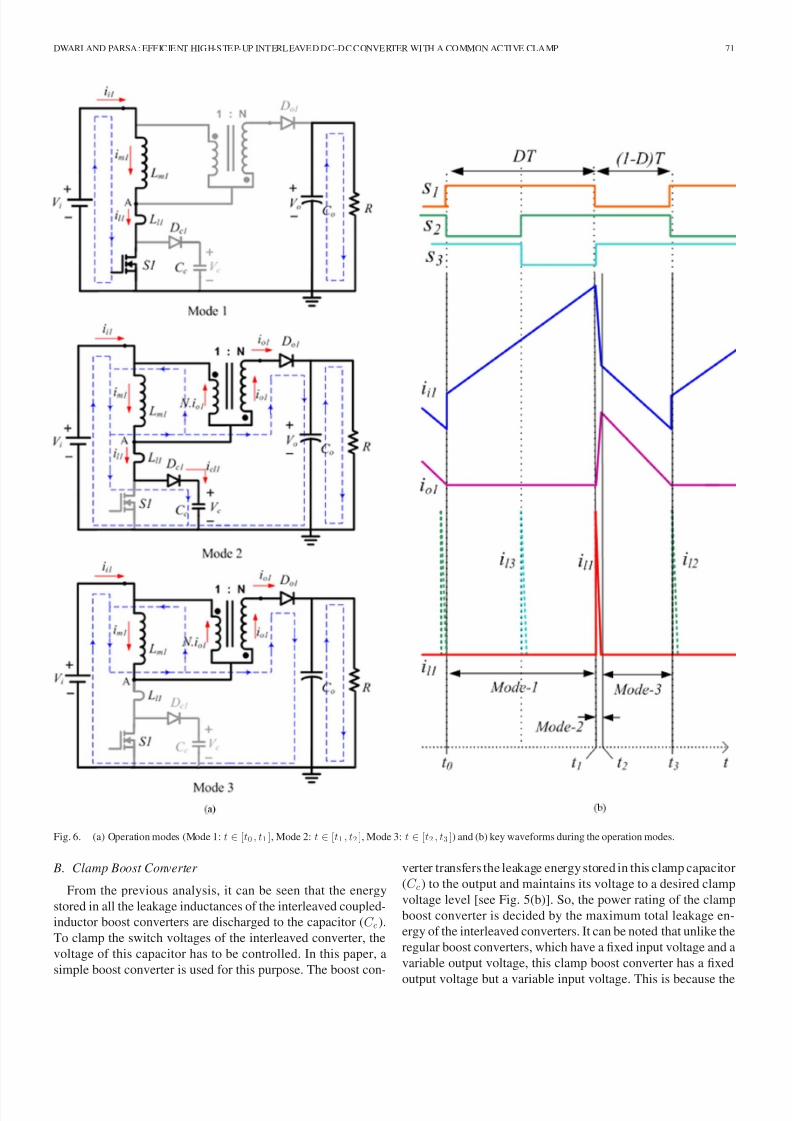
A. Converter Analysis
Consider the nonideal coupled-inductor boost converters are
operated under continuous conduction mode and a boost con-
verter is used for active clamping of the interleaved converters.
Under this condition, there are mainly three modes of operation
in one switching cycle of a coupled-inductor boost converter.
The operation modes for one of the interleaved phases (Phase-1)
are shown in Fig. 6(a). The nonideal coupled inductors of the
interleaved phases can be modeled [see Fig. 6(a)] by a magne-
tizing inductor (Lm 1 ), which is connected in parallel with an
ideal transformer and a series leakage inductor (Ll1 ). The turnsratio of the transformer is equal to the primary to the secondary
turns ratio (1:N ) of the coupled inductor. The value of the mag-
netizing inductance can be obtained by subtracting the leakage
inductance value from the primary winding inductance value of
the coupled inductor. The input current (ii1 ) and the output cur-
rent (io1 ) of the interleaved phase are defined in this equivalent
model, Fig. 6(a). The key waveforms during the three operation
modes are presented in Fig. 6(b). These operation modes are
discussed as follow.
Mode-1(t ∈ [t0 , t1 ]): This mode begins when the switch S 1is turned on. The output diode D1 is reverse biased, and the
input voltage V i charges the primary inductor (Lm 1 ) and theleakage inductor (Ll1 ). The rate of rise of the input current of
the converter can be written as
di1
dt=
vi
Lm 1 + Ll1t ∈ [0, dT ] . (4)
Consider, in steady state, the output power of the Phase-1
of the converter is P o1 and the efficiency of the converter is η.
Using (2) and (4), the peak input current I i1P can be obtained
as
I i1P =P o1
ηV i
1 + N
1 + N D
+V i
2
DT
Ll1 + Lm 1
. (5)
Mode-2(t ∈ [t1 , t2 ]): This mode starts when the switch S 1 is
turned off. The leakage inductor (Ll1 ) forward biases the clamp
diode Dc1 , and the energy stored in the leakage inductor is
discharged to the clamp capacitor C c . This causes a discharge
current spike (icl 1 ). The peak of this current is equal to the
maximum value of the input current (I i1P ), reached at the end
of Mode-1. At the same instant, when the switch S 1 is turned
off, the stored energy in the magnetizing inductor (Lm 1 ) forward
biases diode D1 at the secondary side of the coupled inductor.
The voltage difference between the converter output and the
input (V o − V i ) is divided as per the turns ratio of the ideal
transformer and the voltage at the point A [see Fig. 6(a)] is
defined by (3). It can be noted that the fall rate of the leakage
current is decided by the voltage difference between the clamp-
capacitor voltagevc and the voltage the node A. This can be
presented by (6).
dil1
dt=
N vi + vo
N + 1− vc
1
Ll1t ∈ [t1 , t2 ] . (6)
In steady state, the total fall time for the leakage inductorcurrent τ lf can be obtained from (5) and (6). This can be defined
as
τ lf =I i1P (N + 1)
V c (N + 1) − (N V i + V o )Ll1 t ∈ [t1 , t2 ]. (7)
From(6)and(7),itcanbeseenthatthefalltimeoftheinductor
current can be reduced by increasing the clamp voltage (V c ).
These considerations should be taken into account for designing
the clamp boost converter and the voltage rating of the switches
in the interleaved coupled-inductorboost converters. During this
mode, the current fall rate in the magnetizing inductor can be
found as
dim 1
dt=
vi − vo
N + 1
1
Lm 1t ∈ [t1 , t2 ] . (8)
The output current (io1 ) and the input current (ii1 ) of the
converter can be obtained as
io1 =im 1 − il1
N + 1t ∈ [t1 , t2 ]
ii1 = il1 + io1 =im 1 + N il1
N + 1t ∈ [t1 , t2 ]. (9)
Form (9), it can be seen that the slope of the input and the
output current of the converter during Mode-2 are defined by the
slopes of the magnetizing current (im 1 ) and the leakage inductor
current (il1 ). As the leakage inductance value is much smallerthan the magnetizing inductance value form (6) and (8), it can be
seen that the slopes of the input and the output currents in Mode-
2 are mainly decided by the slope of the leakage inductance
current.
Mode-3(t ∈ [t2 , t3 ]): This mode begins when the leakage in-
ductor current (ii1 ) value has become zero, and the leakage
energy is completely discharged. The clamp diode Dc1 is re-
versed biased by the clamp voltage V c . The output diode D1
remains forward biased and the voltage at the point A is defined
by (3). The energy to the output is transferred form the mag-
netizing inductor and from the source. The switch S 1 remains
turned off.
8/7/2019 power electronics paper
http://slidepdf.com/reader/full/power-electronics-paper 6/13
DWARI AND PARSA: EFFICIENT HIGH-STEP-UP INTERLEAVED DC–DC CONVERTER WITH A COMMON ACTIVE CLAMP 71
Fig. 6. (a) Operation modes (Mode 1: t ∈ [t0 , t1 ], Mode 2: t ∈ [t1 , t2 ], Mode 3: t ∈ [t2 , t3 ]) and (b) key waveforms during the operation modes.
B. Clamp Boost Converter
From the previous analysis, it can be seen that the energy
stored in all the leakage inductances of the interleaved coupled-
inductor boost converters are discharged to the capacitor (C c ).
To clamp the switch voltages of the interleaved converter, the
voltage of this capacitor has to be controlled. In this paper, a
simple boost converter is used for this purpose. The boost con-
verter transfers the leakage energy stored in this clamp capacitor
(C c ) to the output and maintains its voltage to a desired clamp
voltage level [see Fig. 5(b)]. So, the power rating of the clamp
boost converter is decided by the maximum total leakage en-
ergy of the interleaved converters. It can be noted that unlike the
regular boost converters, which have a fixed input voltage and a
variable output voltage, this clamp boost converter has a fixed
output voltage but a variable input voltage. This is because the

8/7/2019 power electronics paper
http://slidepdf.com/reader/full/power-electronics-paper 7/13
72 IEEE TRANSACTIONS ON POWER ELECTRONICS, VOL. 26, NO. 1, JANUARY 2011
total leakage energy of the interleaved converters is very small
compared to the total output power of the interleaved converters.
Therefore, the voltage at the output of the clamp boost converter
is decided by the interleaved coupled-inductor boost converters.
The duty ratio of the clamp boost converter can be controlled to
discharge the leakage energy stored in the clamp capacitor ( C c )
to the output dc bus and maintain its input voltage to a refer-
ence clamp voltage level. The clamp voltage level decides the
voltage stresses on the switches of the coupled-inductor boost
converters. With low switch voltage stress, the converter can be
designed to deliver power at high efficiency even when consid-
erable amount of leakage inductance is present in the couple
inductors. The discussion about the operation of the standard
boost converter is avoided here for brevity. But the design con-
sideration to decide the parameters of the boost converter with
respect to the parameters of the interleaved coupled-inductor
boost converter is presented as follows.
It canbe seen that when theswitch of a coupled-inductor boost
converter is turned off (Mode-2 and Mode-3) and the output
diode is on, the voltage at the common node of the two coupledinductors [point A in Fig. 6(a)] is defined by (3). Therefore,
for successful operation of the active-clamp circuit, the voltage
level at the clamp capacitor (C c ) should be maintained above
the voltage level of the point A. Therefore the lower bound for
the clamp voltage (V c m in ) can be related as
V c m in >N V i + V o
N + 1. (10)
The maximum value of the clamp voltage that can be allowed
can be decided from the information of the maximum voltage
rating of the devices of the interleaved coupled-inductor boost
converter.
Consider the total leakage power from all leakage inductancesis P lt . This leakage power can be obtained as
P lt = f i1
2
nu =1
Llu (I iu P )2 (11)
where f i is the switching frequency of the interleaved coupled-
inductor boost converters, n is the number of total interleaved
phases, and Llu and I iu P are the primary leakage inductance and
the peak primary inductor current in the uth phase, respectively.
The peak currents can be calculated from (5). For simplicity,
it can be considered that the leakage inductances and the peak
currents of the different phases are equal.
The clamp boost converter can be operated either in con-tinuous conduction mode (CCM) or in discontinuous conduc-
tion mode (DCM). Under CCM, the switching losses are more
than the switching losses under DCM. However, the conduction
lossesunder the DCM are more than the conduction lossesunder
the CCM. The clamp boost converter, considered in this study,
processes small amount of power obtained from the leakage in-
ductances of the interleaved converters and the voltage level at
the clamp capacitor (V c mi n ) is quite higher than input voltage
level (V i ). Therefore, the average inductor current of the clamp
boost converter is small. But the MOSFET of the clamp boost
converter switches at high voltage levels. Therefore, in this pa-
per, the clamp boost converter is chosen to operate in DCM to
Fig. 7. (a) From top to bottom: gate pulses to the three interleaved converter(n = 3), gate pulses to theclampboost converter,and theinductor current of theclampboost converter, and (b) control circuit block diagram for the clamp-boostconverter.
reduce the losses in the clamp boost converter. The gate pulses
to the MOSFET of the clamp boost converter and the current inthe boost inductor under DCM operation are shown in Fig. 7(a).
Consider the operating duty cycle, the switching frequency and
the inductance value of the clamp boost converter are Dc , f c ,
and Lb , respectively. Under DCM operation, the average in-
put power of the clamp boost converter, supplied by the clamp
capacitor C c can be derived as
P ib =1
2
V 2c D2
c
f c Lb
1
1 − V c /V o
. (12)
Under steady-state condition, the average leakage power (P lt )
discharged to the clamp capacitor should be equal to the average
input power of the boost converter (P ib ). Therefore, using (11)
and (12) the value of the boost inductor can be obtained as
in (13). This calculation can be used for designing the boost
inductor.
Lb =1
f i f c
V 2c D2
cnu =1 Llu (I iu P )2
1
1 − V c /V o
. (13)
To clamp the voltage stresses on the switches of the inter-
leaved coupled-inductor boost converters to a low level, the
voltage of the clamp capacitor should be maintained at a desired
reference value. To achieve this, the clamp-capacitor voltage
(the input of the clamp boost converter) is sensed and the clamp
boost converter is controlled in a closed loop. Theblock diagram

8/7/2019 power electronics paper
http://slidepdf.com/reader/full/power-electronics-paper 8/13
DWARI AND PARSA: EFFICIENT HIGH-STEP-UP INTERLEAVED DC–DC CONVERTER WITH A COMMON ACTIVE CLAMP 73
of the closed-loop control scheme applied to the clamp-boost
converter is presented in Fig. 7(b). Based on the error informa-
tion between the sensed clamp capacitor voltage (vb ) and the
reference clamp voltage (v∗br ), a suitable controller is used to
estimate the duty cycle of the converter. It can be noted that,
in the clamp-boost converter, the input voltage decreases with
the increase of the duty cycle. Therefore, in this paper, the error
information is obtained by subtracting the reference clamp volt-
age from the measured clamp-capacitor voltage. The estimated
voltage of the controller is used by a pulse width modulation
controller to generate the gate pulses for the switch of the clamp
boost converter. A suitable driver is used to drive the MOSFET
of the converter.
It can be mentioned that, for n = 3, the frequency of the volt-
age ripple at the output capacitor of the interleaved coupled-
inductor boost converter is three times the switching fre-
quency of each interleaved coupled-inductor boost converter
[see Figs. 4(b) and 5(b)]. For this reason, in this paper, the
switching frequency of the clamp boost converter is chosen
to be three times the switching frequency of the interleavedconverters(f c = 3f i ).
IV. DESIGN GUIDELINES
Considering the standard power train architectures of the EV,
HEV, FCV, and telecom power systems [1]–[4], [9], and [10],
in this paper, the nominal input voltage and the output volt-
age of the converter are chosen as 42 and 350 V, respec-
tively. Therefore, the voltage step-up ratio of the converter is
V o /V i = 8.33. As discussed earlier, in Section II, the number
of interleaved phases of the converter is n = 3 and for optimal
performance of interleaved converter, the chosen nominal duty
ratio is D = 0.66. The key converter design step is the selection
of turns ratio of the coupled inductors (N ), which can perform
the required voltage step-up operation while operating at the
selected nominal duty ratio. To consider effect of the leakage
inductance on the voltage step-up ratio of the coupled-inductor
boost converter, volt–second balance can applied both on the
magnetizing inductor (Lm 1 ) and on the leakage inductor of a
coupled-inductor boost converter(Ll1 ). The voltage gain of the
converter can be obtained as
V oV i
= 1 +D(1 + N )
1 − DK, K =
Lm 1
Lm 1 + Ll1. (14)
Fig. 8 presents the design plots for the voltage gain (V o /V i )versus duty ratio (D) of a coupled-inductor boost converter for
different turns ratios(N ). In this figure, the value of K = 0.97.Appropriate turns ratio of the converter can be selected from
the chart by using the voltage gain and nominal duty cycle
information.
The voltage rating of the switches of the coupled-inductor
boost converters is decided by the value of clamp voltage and
the safety margin. The clamp voltage is mainly decided by the
voltage at the common node of the coupled inductors (V cl ), dur-
ing the turn-OFF period of the switches. Therefore, the voltage
V cl is a key design parameter that has to be obtained. Using (3)
and (14), the ratio between the voltage V cl and the input voltage
Fig. 8. Design plot: voltage gain of the converter (Vo/Vi) versus duty ratio (D)for different turns ratios (N ); (K = 0.97).
V i can be expressed as following (15).
V cl
V i=
DK −D + 1
1 −D. (15)
Interestingly, it can be found that, when N = 0, the output
voltage to input voltage gain (V o /V i ) in (14) is equal with the
ratio between the voltage V cl and the input voltage V i in (15).
Therefore, the design curve for N = 0, in Fig. 8, can be used to
obtain the value of the voltage V cl . Based of the values of V cl ,
leakage inductance, peak of the primary inductor current, and
the clamp voltage of the interleaved converter can be designed
(5, 7, and 15).
To select the diodes in the secondary side of the interleaved
coupled-inductor boost converters, the maximum reverse-bias
voltage, the peak forward current, and the average forward cur-
rent in the diodes are to be known. It can be seen from Fig. 6,
when the switch is turned on (Mode-1), the secondary side diode
Do1 remains turned off, and the input voltage is applied across
the primary side winding of the coupled inductor. The voltage
applied across the primary side of the coupled-inductor will
be reflected on its secondary side. Therefore, under this con-
dition, the maximum reverse-bias voltage, V D or applied across
the secondary side diode Do1 can be obtained as
V D or = V iLm 1
Lm 1 + Ll1N − V i
Ll
Lm 1 + Ll1+ V o . (16)
Considering that the leakage inductance Ll1 is smaller com-pared to the magnetizing inductance Lm 1 , (16) can be simplified
as
V D or = V i N + V o . (17)
The maximum reverse-bias voltage applied across the sec-
ondary side diode can be obtained by using the aforementioned
equation.
Under steady state, the average current through the secondary
diode of an interleaved coupled-inductor boost converter (e.g.,
Do1 in Phase-1) can be obtained by applying the charge balance
theory on the output capacitor. Therefore, it can be perceived
that the average forward current in the secondary diode is equal

8/7/2019 power electronics paper
http://slidepdf.com/reader/full/power-electronics-paper 9/13
74 IEEE TRANSACTIONS ON POWER ELECTRONICS, VOL. 26, NO. 1, JANUARY 2011
TABLE IKEY PARAMETERS OF THE CONVERTER
to the output dc current of the interleaved phase. The peak value
of the pulsating current through the secondary side diode is
decided by the input peak current I i1P (5) of the phase; reached
at the end of Mode-I, Fig. 6(b). Considering that the energy
stored in the leakage inductor is very small compared to theenergy stored in the magnetizing inductor, the peak value of
current I i2P in the secondary side diode can be obtained as
I i2P = I i1P 1
1 + N =
P o1
ηV i
1
1 + N D
+V i2
DT
Ll1 + Lm 1
1
1 + N . (18)
The peak forward current rating of the secondary side diodes
can be decided by using the aforementioned (18). The peak
forward current in the clamp diodes (e.g., Dc1 in Phase-1) of
the proposed active-clamp circuit (see Fig. 6) is equal to the
input peak current I i1P . Therefore, (5) can be used to calculatethe peak forward current rating of the clamp diodes.
V. SIMULATION RESULTS
A 42 to 350 V step-up converter with nominal output power
rating of 1500 W is designed and simulated to verify the pro-
posed concept. Converter analysis and design guidelines, pre-
sented in the previous sections, are used for this purpose. The
converter consists of three interleaved coupled-inductor boost
converters and a common clamp boost converter.
Simulations of the converter are carried out in SABER. The
key converter parameters are listed in Table I. The estimated
leakage inductance of the converter is 1.7 μH. The interleavedconverter is designed to operate at a switching frequency of
25 kHz. The calculated lower limit of the clamp voltage of
the designed converter is about 120 V. To limit the fall time
of the leakage inductor current to about 2 μs, the clamp volt-
age level of the converter is designed to be 140 V (5, 7). This
clamp voltage value decides the maximum voltage stress of the
switches of the coupled-inductor boost converter. The selected
MOSFET for the interleaved coupled-inductor boost converter
is STW75NF20 (200 V, Rds−ON = 33 mΩ; STMicroelectron-
ics). In each interleaved phase, three MOSFETs are connected
in parallel to realize the switch. The output diode selected for the
converter is FFH30S60 S (600 V; Fairchild Semi.). The switch
Fig. 9. (a) Drain-to-source voltage of the switch in a coupled-inductor boostconverter without anyclampingand (b) output voltage,clamp voltage and drain-to-source voltage of the switch in a coupled-inductor boost converter with theproposed active-clamp circuit.
selected for the clamp boost converter is STP17NK40Z (400 V,
ST Micro.). These device models are used in the simulation.The simulated voltage stress across the MOSFETs of the
interleaved converter, when no clamping circuit is employed,
is shown in Fig. 9(a). The voltage across the MOSFETs of the
interleaved converters with the common clamp boost converter
is shown in Fig. 9(b). It can be seen that the high voltage spikes
caused by the leakage inductors can be successfully reduced to
a lower level by the proposed clamp boost converter. The output
voltage level and the clamp voltage levels of the converter under
full-load condition are also presented in Fig. 9(b).
The total input current of the converter is presented in
Fig. 10(a). The currents in the primary inductors of the three
phases of the interleaved converter are also shown in this figure.
It can be seen that the phase currents are equal in amplitude andphase shifted by 120◦. The primary current, secondary current,
and leakage inductor current of one phase of the interleaved con-
verter are shown in Fig. 10(b). From this figure, it can be seen
that the energy stored in the leakage inductance is discharged to
the clamp-capacitor in the form of a current spike. These simu-
lations results agree with the analysis of the converter presented
in Section III. The current in the inductor of the clamp boost
converter and the gate pulses to the MOSFET of the clamp boost
converter are shown in Fig. 11. It is calculated from the simu-
lation and the previous analysis that the total leakage energy of
the interleaved coupled-inductor boost converter is 44.2 W. The
estimated efficiency of the converter is 95.4%. The simulation
8/7/2019 power electronics paper
http://slidepdf.com/reader/full/power-electronics-paper 10/13
DWARI AND PARSA: EFFICIENT HIGH-STEP-UP INTERLEAVED DC–DC CONVERTER WITH A COMMON ACTIVE CLAMP 75
Fig. 10. (a) From top to bottom: total input current of the converter, inputcurrents of the interleaved coupled-inductor boost converters, and (b) primarycurrent, secondary current, and leakage current in a phase of the interleavedcoupled-inductor boost converters.
Fig. 11. (a) Gate pulses to the clamp boost converter and (b) inductor currentof the clamp boost converter.
results show that the proposed converter can successfully handle
the high-input current and perform voltage-step-up operation at
a high efficiency.
It can be mentioned that if the proposed boost converter based
active clamping circuit is not used, the leakage energy cannot
be recycled. Therefore, due to the large voltage stresses [see
Fig. 9(a)], MOSFETs of much higher voltage ratings, which
have large ON-state resistances RD S -ON have to be used to
realize the switches of the interleaved converters. Furthermore,
additional losses will occur due to the parasitic ringing in the
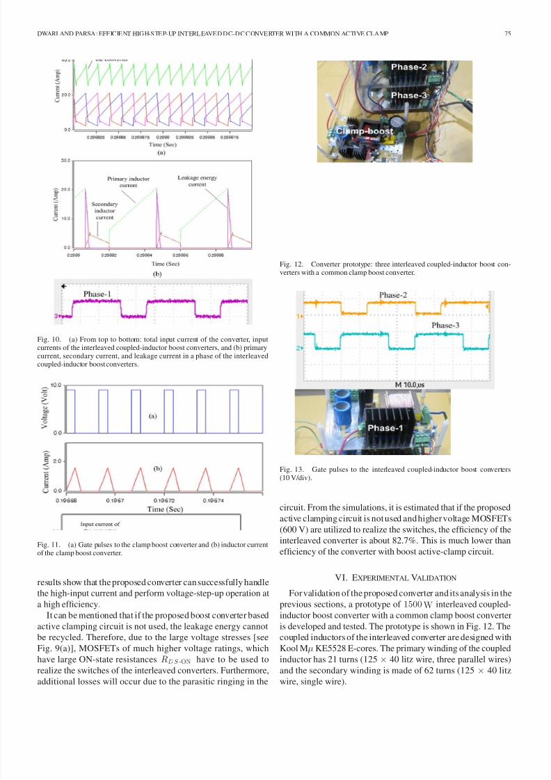
Fig. 12. Converter prototype: three interleaved coupled-inductor boost con-
verters with a common clamp boost converter.
Fig. 13. Gate pulses to the interleaved coupled-inductor boost converters(10 V/div).
circuit. From the simulations, it is estimated that if the proposed
active clamping circuit is not used and higher voltage MOSFETs
(600 V) are utilized to realize the switches, the efficiency of the
interleaved converter is about 82.7%. This is much lower than
efficiency of the converter with boost active-clamp circuit.
VI. EXPERIMENTAL VALIDATION
For validation of the proposed converter and its analysis in the
previous sections, a prototype of 1500 W interleaved coupled-
inductor boost converter with a common clamp boost converter
is developed and tested. The prototype is shown in Fig. 12. The
coupled inductors of the interleaved converter are designed with
Kool Mμ KE5528 E-cores. The primary winding of the coupled
inductor has 21 turns (125 × 40 litz wire, three parallel wires)
and the secondary winding is made of 62 turns (125 × 40 litz
wire, single wire).

8/7/2019 power electronics paper
http://slidepdf.com/reader/full/power-electronics-paper 11/13

8/7/2019 power electronics paper
http://slidepdf.com/reader/full/power-electronics-paper 12/13
DWARI AND PARSA: EFFICIENT HIGH-STEP-UP INTERLEAVED DC–DC CONVERTER WITH A COMMON ACTIVE CLAMP 77
Fig. 19. From top to bottom: gate pulses to the clamp boost converter(10 V/div) and inductor current of the clamp boost converter (1 A/div).
TABLE IILOSS DISTRIBUTION
value of the input current is 37.65 A. The leakage current in
phase-1 of the interleaved converter and the input current of that
phase are presented in Fig. 17. The slope of the leakage current
is decided by the leakage inductor and the voltage differencebetween the clamp voltage and the voltage at the common node
of the primary and secondary inductors. It can be seen that the
fall time of the leakage current is close to 2μs. The measured
leakage currents from all the three interleaved coupled-inductor
boost converters, which charge the clamp capacitor, are pre-
sented in Fig. 18. These measurements agree with the previous
analysis and simulation results. The gate pulses to the MOS-
FET of the clamp boost converter and the inductor current in
that converter are presented in Fig. 19. As per the presented
design, the clamp boost converter is operated under DCM. The
operating duty cycle of the clamp boost converter, estimated by
the controller, is 0.28. It is obtained from the measurements that
the average leakage power of the interleaved converters is about
47.5 W, which matches with the previous calculation.
To find the loss distribution in the converter, the currents and
voltages in different components are measured or estimated.
The various loss components in the converter are presented in
Table II. The efficiency of the converter, calculated from this
loss analysis is about 95.1%. The measured efficiency of the
converter is about 94.8%. Therefore, it can be seen that the
proposed interleaved coupled-inductor boost converters with a
common boost clamp can perform high-step-up operation with
high efficiency.
VII. CONCLUSION
Coupled-inductor boost converters can be interleaved to
achieve high-step-up power conversion without extreme duty
ratio operation while efficiently handling the high-input cur-
rent. In a practical coupled-inductor boost converter, the switch
is subjected to high voltage stress due to the leakage inductance
present in the nonideal coupled inductor. The presented active-clamp circuit, based on single boost converter, can successfully
reduce the voltage stress of the switches close to the low-level
voltage stress offered by an ideal coupled-inductor boost con-
verter. The common clamp capacitor of this active-clamp circuit
collects the leakage energies from all the coupled-inductor boost
converters, and the boost converter recycles the leakage ener-
gies to the output. Detailed analysis of the operation and the
performance of the proposed converter were presented in this
paper. It has been found that with the switches of lower voltage
rating, the recovered leakage energy, and the other benefits of
an ideal coupled-inductor boost converter and interleaving, the
converter can achieve high efficiency for high-step-up power
conversion. A prototype of the converter was built and tested
for validation of the operation and performance of the pro-
posed converter. The experimental results agree with the analy-
sis of the converter operation and the calculated efficiency of the
converter.
REFERENCES
[1] L. Solero, A. Lidozzi, and J. A. Pomilio, “Design of multiple-input powerconverter for hybrid vehicles,” IEEE Trans. Power Electron., vol. 20,no. 5, pp. 107–116, Sep. 2005.
[2] A. A. Ferreira, J. A. Pomilio, G. Spiazzi, and de Araujo Silva, “Energymanagement fuzzy logic supervisory for electric vehicle power suppliessystem,” IEEE Trans. Power Electron., vol. 20, no. 1, pp. 107–115, Jan.2008.
[3] A. Emadi, K. Rajashekara, S. S. Williamson, and S. M. Lukic, “Topo-logical overview of hybrid electric and fuel cell vehicular power systemarchitectures and configurations,” IEEE Trans. Veh. Technol., vol. 54,no. 3, pp. 763–770, May 2007.
[4] J. Baumanand M.Kazerani, “A comparativestudyof fuel cell-battery, fuelcell-ultracapacitor, and fuel cell-battery-ultracapacitor vehicles,” IEEE
Trans. Veh. Technol., vol. 57, no. 2, pp. 760–769, Mar. 2008.[5] Q. Zhao and F. C. Lee, “High-efficiency, high step-up DC–DC con-
verters,” IEEE Trans. Power Electron., vol. 18, no. 1, pp. 65–73, Jan.2003.
[6] I. Barbi and R. Gules, “Isolated DC-DC converters with high-output volt-age for TWTA telecommunication satellite applications,” IEEE Trans.
Power Electron., vol. 18, no. 4, pp. 975–984, 2003.[7] A. Reatti, “Low-cost high power-density electronic ballast for automotive
HID lamp,” IEEE Trans. Power Electron., vol. 15, no. 2, pp. 361–368,
Mar. 2000.

8/7/2019 power electronics paper
http://slidepdf.com/reader/full/power-electronics-paper 13/13
78 IEEE TRANSACTIONS ON POWER ELECTRONICS, VOL. 26, NO. 1, JANUARY 2011
[8] M. Veerachary, T. Senjyu, and K. Uezato, “Neural-network-basedmaximum-power-point tracking of coupled-inductor interleavedboost-converter-supplied PV system using fuzzycontroller,” IEEE Trans. Power
Electron., vol. 8, no. 4, pp. 749–758, Aug. 2003.[9] J. Marshall andM. Kazerani, “Design of an efficient fuel cell vehicle drive
train, featuring a novel boost converter,” in Proc. IEEE Ind. Electron. Soc.
Annu. Conf., Nov. 2004, pp. 1229–1234.[10] G. C.-Lopez, A. J. Forsyth, and D. R. Nuttall, “Design and performance
evaluation of a 10-kW interleaved boost converter for a fuel cell electricvehicle,”in Proc. IEEE Power Electron. MotionControl Conf., Aug. 2006,vol. 2, pp. 1–5.
[11] E. J. Cegnar, H. L. Hess, and B. K. Johnson, “A purely ultracapacitorenergy storage system hybrid electric vehicles utilizing a based DC-DCboost converter,” in Proc. Appl. Power Electron. Conf. Expo., IEEE , 2004,vol. 2, pp. 1160–1164.
[12] N. Mohan, T. M. Undeland, and W. P. Robbins, Power Electronics,3rd ed. New York: Wiley, 2002.
[13] K. Hirachi, M. Yamanaka, K. Kajiyama, and S. Isokane, “Circuit config-uration of bidirectional DC/DC converter specific for small scale loadingsystem,” in Proc. IEEE Power Convers. Conf., 2002, pp. 603–609.
[14] C. Y. Inaba, Y. Konishi, and M. Nakaoka, “High frequency PWM con-trolled step-up chopper type DC-DC power converters with reduced peak switch voltage stress,” in Proc. IEE Proc.- Electr. Power Appl., Jan. 2004,pp. 47–52.
[15] C. M. C. Duarte and I. Barbi, “An improved family of ZVS-PWM active-
clamping DC-to-DC converters,” IEEE Trans. Power Electron., vol. 17,no. 1, pp. 1–7, Jan. 2002.[16] W. Rong-Jong and D. Rou-Yong, “High step-up converter with coupled-
inductor,” IEEE Trans. Power Electron., vol. 20, no. 5, pp. 1025–1035,Sep. 2005.
[17] W. Rong-Jong and D. Rou-Yong, “High-efficiency power conversion forlow power fuel cell generation system,” IEEE Trans. Power Electron.,vol. 20, no. 4, pp. 847–856, Jul. 2005.
[18] C. Chang and M. A. Knights, “Interleaving technique in distributed powerconversion systems,” IEEE Trans. Circuits Syst. I: Fund. Theory Appl.,vol. 42, no. 5, pp. 245–250, May 1995.
[19] M. T. Zhang, M. M. Jovanovic, and F. C. Lee, “Analysis and evaluationof interleaving techniques in forward converters,” IEEE Trans. Power
Electron., vol. 13, no. 4, pp. 690–698, Jul. 1998.[20] S. Dwari and L. Parsa, “A novel high efficiency high power interleaved
coupled-inductor boost DC-DC converter for hybrid and fuel cell electricvehicle,” in Proc. IEEE Veh. Power Propulsion Conf. 2007 , pp. 399–404.
[21] W. Li and X. He, “An interleaved winding-coupled boost converter withpassive lossless clamp circuits,” IEEE Trans. Power Electron., vol. 22,no. 4, pp. 1499–1507, Jul. 2007.
[22] W. Li and X. He, “A family of interleaved DC–DC converters deducedfrom a basic cell with winding-cross-coupled inductors (WCCIs) for highstep-up or step-down conversions,” IEEE Trans. Power Electron., vol. 23,no. 4, pp. 1791–1801, Jul. 2008.
[23] K. Hirachi, M. Yamanaka, K. Kajiyama, and S. Isokane, “Circuit config-uration of bidirectional DC/DC converter specific for small scale loadingsystem,” in Proc. IEEE PCC-Osaka, 2002, vol. 2, pp. 603–609.
[24] S. Dwari, S. Jayawant, T. Beechner, S. K. Miller, A. Mathew, M. Chen,J. Riehl, andJ. Sun,“Dynamics characterization of coupled-inductor boostDC-DC converters,” in Proc. Comput. Power Electron., IEEE Workshop,Jul. 2006, pp. 264–269.
Suman Dwari (S’05) received the M.Tech. degreein electrical engineering from the Indian Institute of Technology, Bombay, India, in 2003. He is currentlyworking toward the Ph.D. degree in electrical en-gineering at the Department of Electrical, Computer,andSystems Engineering, Rensselaer Polytechnic In-stitute, Troy, NY.
From 2003 to 2004, he was a Design Engineer inpower electronics industry. From 2004 to 2005, hewas a Senior Research Assistant at the Departmentof ElectricalEngineering,Indian Instituteof Technol-
ogy. His current research interests are special electrical machines, fault tolerantac drives, efficient power-converters, energy harvesting, power electronic sys-tems, and embedded control.
Leila Parsa (S’00–M’05) received the Ph.D. degreein electrical engineering from Texas A&M Univer-sity, College Station.
Since 2005, she has been an Assistant Professorat the Department of Electrical, Computer, and Sys-tems Engineering, Rensselaer Polytechnic Institute,Troy, NY. Her current research interests include de-
sign, analysis, and control of electromechanical en-ergy converters and power electronics converters forvarious applications.
Dr. Parsa is the recipient of the 2009 Office of Naval Research Young Investigator Award, the 2007 IEEE Industry Applica-tions Society Outstanding Young Member Award, and the 2006 IEEE IndustryApplications Society Transactions Paper Award.