Embed Size (px)
Citation preview
www.irf.com 1
AN-1167
Application Note AN-1167
Power Factor Correction using IR1153 Fixed Frequency CCM PFC IC
By Ramanan Natarajan, Helen Ding, Ron Brown
Table of Contents
IR1153 Detailed Description PFC Converter Design Procedure using IR1153 For additional data, please visit our website at:
http://www.irf.com
Keywords: PFC, Power Factor Correction, THD.
www.irf.com 2
AN-1167
RSNS
RBOP1
RBOP2
RBOP3
RSF
CSF
CIN
COUT
LBST
CZ
CPCBOP
Rgm
RVFB1
RVFB2
RVFB3
ROVP1
ROVP2
ROVP3
AC Line
AC Neutral
IR1145
VOUT
VCC
GND
DBST
MBST
Bridge
CVCC
RG
COM
- +
COM1
BOP4
VFB6
VCC7
GATE8
ISNS3
COMP2
OVP/EN5
RSNS
RBOP1
RBOP2
RBOP3
RSF
CSF
CIN
COUT
LBST
CZ
CPCBOP
Rgm
RVFB1
RVFB2
RVFB3
ROVP1
ROVP2
ROVP3
AC Line
AC Neutral
IR1145
VOUT
VCC
GND
DBST
MBST
Bridge
CVCC
RG
COM
- +
COM1
BOP4
VFB6
VCC7
GATE8
ISNS3
COMP2
OVP/EN5
1. Introduction The IR1153 IC is a fixed 22.2kHz frequency PFC IC designed to operate in continuous conduction mode Boost converters with average current mode control. The IC is packed with an impressive array of advanced features such as programmable soft-start, micro-power startup current, user initiated micro-power Sleep mode for compliance with stand-by energy standards and ultra low bias currents for sensing pins. The fixed internal oscillator ensures stable operation at 22.2kHz switching frequency with very low gate jitter thus eliminating audible noise in PFC magnetics. In addition, the IC offers input-line sensed brown-out protection (BOP), dedicated overvoltage protection, cycle-by-cycle peak current limit, open loop protection (OLP) and VCC under voltage lock-out (UVLO). All these features are offered in a compact 8-pin package making IR1153 the most feature-intensive IC for PFC applications. This application note provides an overview of the IR1153 and demonstrates the design of a universal input 2000W AC-DC Boost PFC Converter. Design & layout tips are also included.
2. IR1153 – Detailed Description 2.1 Overview of IR1153
Fig.1: Typical application diagram of IR1153 based PFC converter Fig.1 shows the system application diagram of the IR1153 based PFC converter. Only 3 pin functionalities - VFB, COMP & ISNS – are actually needed to obtain the necessary diagnostic signals to achieve power factor correction and maintain output voltage regulation. The functions of the abovementioned 3 pins are as follows:
IR1153
www.irf.com 3
AN-1167
• VFB – provides DC bus voltage sensing for voltage regulation
• COMP – used for compensating the voltage feedback loop to set the correct transient response characteristics
• ISNS – provides sensing of the inductor current, which is used to determine the PFC switch duty cycle
Essentially, there are 2 control loops in the PFC algorithm:
• a slow, outer voltage loop whose function is to simply maintain output voltage regulation
• a fast inner current loop whose function is to determine the instantaneous duty cycle every switching cycle
The current shaping function i.e. power factor correction is achieved primarily by the current loop. The voltage loop is responsible only for controlling the magnitude of the input current in order to maintain DC bus voltage regulation. 2.2 Key Features of IR1153 Fixed 22.2kHz Frequency Internal Oscillator IR1153 features a fixed frequency internal oscillator running at 22.2kHz. The gate drive pulse is completely free of jitter and this greatly enables elimination of audible noise in PFC magnetics due to magnetostriction. Also internalization of the oscillator greatly improves noise immunity of the IC. Programmable soft-start IR1153 facilitates programmability of system soft-start time thus allowing the designer some freedom (taking into consideration the loop compensation characteristics) to choose the converter start-up times appropriate for the application. The soft start time is the time required for the VCOMP voltage to charge through its entire dynamic range i.e. 0V through VCOMP,EFF. As a result, the soft-start time is dependent upon the component values selected for compensation of the voltage loop on the COMP pin – primarily the CZ capacitor (described in detail in Soft-Start Design section of PFC Converter Design portion of this document). As VCOMP voltage rises gradually, the IC allows a higher and higher RMS current into the PFC converter. This controlled increase of the input current contributes to reducing system component stress during start-up. It is clarified that, during soft-start, the IC is capable of full duty cycle modulation (from 0% to MAX DUTY), based on the instantaneous ISNS signal from system current sensing. Furthermore, the internal logic of the IC is designed to ensure that the soft-start capacitor is discharged when the IC enters the Sleep or Stand-by modes in order to facilitate soft-start upon restart.
www.irf.com 4
AN-1167
User initiated micro-power sleep mode The IR1153 has an ENABLE function embedded in the OVP/EN pin. When this pin voltage is actively pulled below VSLEEP threshold, the IC is pushed into the Sleep mode where the current consumption is less than 75uA even when VCC is above VCC,ON threshold. The system designer can use an external logic level signal to access the ENABLE feature since VSLEEP threshold is so low. The IR1153 internal logic ensures that VCOMP is discharged before the IC enters Sleep mode in order to enable soft-start upon resumption of operation. Protection features The IR1153 features a comprehensive array of protection features to safeguard the system. These are explained below. 1. Dedicated & Programmable Overvoltage protection (OVP) The OVP pin is a dedicated pin for overvoltage protection that safeguards the system even if there is a break in the VFB feedback loop due to resistor divider failure etc. An overvoltage fault is triggered when OVP pin voltage exceeds the VOVP threshold of 106%VREF. The IC gate drive is immediately disabled and held in that state. The overvoltage fault is removed and gate drive re-enabled only when both pin voltages are below the VOVP,RST threshold of 103% VREF. The exact voltage level at which overvoltage protection is triggered can be programmed by the user by carefully designing the OVP pin resistor divider. It is recommended NOT to set the OVP voltage trigger limit less than 106% of DC bus voltage, since this can endanger the situation where the OVP reset limit will be less than the DC bus voltage regulation point – in this condition the voltage loop can become unstable. 2. Open-Loop protection (OLP) The open-loop protection ensures that the IC is restrained in the Stand-by mode if the VFB pin voltage has not exceeded or has dropped below VOLP threshold of 19%VREF. In the Stand-by mode, all internal circuitry of the IC are biased, the gate drive is disabled and current consumption is a few milliamps. During start-up, if for some reason the voltage feedback loop is open then IC will remain in Stand-by and not start thus avoiding a potentially catastrophic failure. 3. Brown-Out protection (BOP) IR1153 provides brown-out protection based on direct sensing of AC input line. Information about the rectified AC input voltage is communicated to the BOP pin after scaling it down using a resistor divider network and filtering using a capacitor on BOP pin. During start-up, the IC is held in Stand-by mode when BOP pin voltage is less than VBOP(EN) threshold of 1.56V. When the pin voltage exceeds this threshold, the IC enters normal operation (assuming no OLP condition exists). Subsequently, if the pin voltage falls below VBOP threshold of
www.irf.com 5
AN-1167
0.76V during normal operation, then a brown-out fault is detected and IC is pushed into Stand-by mode. For the IC to exit Stand-by, the pin voltage has to exceed VBOP(EN) threshold again. In the Stand-by mode, all internal circuitry of the IC are biased, the gate drive is disabled and current consumption is a few milliamps. 4. Cycle-by-cycle peak current limit protection (IPK LIMIT) The cycle-by-cycle peak current limit is encountered when VISNS pin voltage exceeds VISNS(PK) threshold of -0.51V (in magnitude). When this condition is encountered, the IC gate drive is immediately disabled and held in that state until the ISNS pin voltage falls below VISNS(PK). Even though the IR1153 operates based on average current mode control, the input to the peak current limit comparator is decoupled from the averaging circuit thus enabling instantaneous cycle-by-cycle protection for peak current limitation. 5. VCC UVLO In the event that the voltage at the VCC pin should drop below that of the VCC UVLO turn-off threshold, VCC(UVLO) the IC is pushed into the UVLO mode, the gate drive is terminated, and the turn on threshold, VCC, ON must again be exceeded in order to re start the process. In the UVLO mode, the current consumption is less than 75uA.
3. PFC Converter Design Procedure
3.1 PFC Converter Specifications
AC Input Voltage Range 170-264VAC
Input Line Frequency 47-63Hz
Nominal DC Output Voltage 385V +/- 5%
DC Bus Overvoltage Limit 425V
Nominal Output Power 2000W
Power Factor 0.99 @ 230VAC/350W
Output Holdup Time 20ms @ VOUT,MIN=285V
Start-up time 300ms
Table 1: Design Specifications for PFC Converter
www.irf.com 6
AN-1167
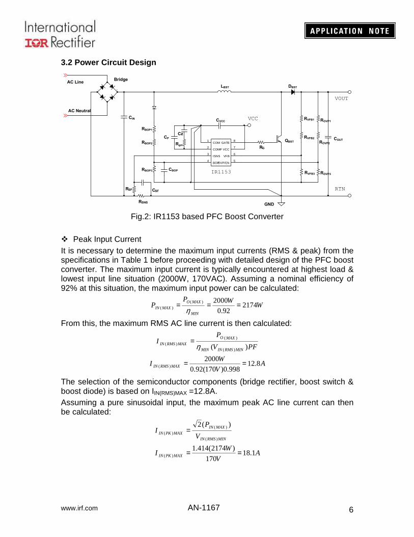
3.2 Power Circuit Design
RSNS
RBOP1
RSF CSF
CIN
AC Line
AC Neutral
GND
Bridge
RG
COM1
BOP4
VFB6
VCC7
GATE8
ISNS3
COMP2
OVP/EN5
IR1153
VOUT
RTN
VCC
- +
RBOP2
RBOP3 CBOP
LBST DBST
RVFB1
RVFB2
RVFB3
ROVP1
ROVP2
ROVP3
COUT
CVCC
CPCz
RgmQBST
Fig.2: IR1153 based PFC Boost Converter
Peak Input Current It is necessary to determine the maximum input currents (RMS & peak) from the specifications in Table 1 before proceeding with detailed design of the PFC boost converter. The maximum input current is typically encountered at highest load & lowest input line situation (2000W, 170VAC). Assuming a nominal efficiency of 92% at this situation, the maximum input power can be calculated:
WWP
PMIN
MAXO
MAXIN 217492.0
2000)(
)( ===η
From this, the maximum RMS AC line current is then calculated:
AV
WI
PFV
PI
MAXRMSIN
MINRMSINMIN
MAXO
MAXRMSIN
8.12998.0)170(92.0
2000
)(
)(
)(
)(
)(
==
=η
The selection of the semiconductor components (bridge rectifier, boost switch & boost diode) is based on IIN(RMS)MAX =12.8A. Assuming a pure sinusoidal input, the maximum peak AC line current can then be calculated:
AV
WI
V
PI
MAXPKIN
MINRMSIN
MAXIN
MAXPKIN
1.18170
)2174(414.1
)(2
)(
)(
)()(
==
=
www.irf.com 7
AN-1167
Boost Inductance (LBST) IR1153 IC is an average current mode controller. An on-chip RC filter is sized to effectively filter the boost inductor current ripple to generate a clean average current signal for the IC. The averaging function in the IC can accommodate a maximum limit of 40% inductor current ripple factor at maximum input current. The boost inductance has to be sized so that the inductor ripple current factor is not more than 40% at maximum input current condition (at peak of AC sinusoid). This is because: • Higher ripple current factors will interfere with the Average Current Mode
operation of One Cycle Control algorithm in IR1153 leading to duty cycle instabilities and pulse skipping which results in current distortion and sometimes even audible noise
• power devices are stressed more with higher ripple currents as the peak inductor current (IL(PK)MAX) also increases proportionately
In this calculation, an inductor current ripple factor of 35% is selected (typical ripple factor is ~20% for most PFC designs). The ripple current at peak of AC sinusoid at maximum input current is:
AAI
II
L
MAXPKINL
3.61.1835.0
35.0 )(
=×=∆×=∆
And, peak inductor current is:
AA
AI
III
MAXPKL
LMAXPKINMAXPKL
3.212
3.61.18
2
)(
)()(
=+=
∆+=
In order to determine the boost inductance, the power switch duty cycle at peak of AC sinusoid (at lowest input line of 170VAC) is required.
VVV MINRMSINMINPKIN 2402 )()( =×=
Based on the boost converter voltage conversion ratio,
38.0385
240385
V )(
=−=
=
V
VVD
V
VD
O
MINPKINO
The boost inductance is then given by:
AkHz
V
If
DVL
LSW
MINPEAKINBST 3.62.22
38.0240)(
××=
∆××
=
HLBST µ652=
A convenient value of 700µH is selected for LBST for this converter.
www.irf.com 8
AN-1167
High Frequency Input Capacitor (CIN) The purpose of the high-frequency capacitor is to supply the high-frequency component of the inductor current (the ripple component) via the shortest possible loop. This has the advantage of acting like an EMI filter, since it minimizes the high-frequency current requirement from the AC line. Typically a high-frequency, film type capacitor with low ESL and high-voltage rating (630V) is used. High-frequency input capacitor design is essentially a trade-off between: • sizing it big enough to minimize the noise injected back into the AC line • sizing it small enough to avoid line current zero-crossing distortion (flattening) The high-frequency input capacitor is determined as follows:
FCVkHz
AC
Vrf
IkC
IN
IN
MINRMSINSW
MAXRMSIN
IIN L
µπ
π
1.217009.02.222
8.1235.0
2 )(
)(
=×××
=
×××= ∆
where: k∆IL = inductor current ripple factor, of 35% as mentioned earlier r = maximum high frequency input voltage ripple factor (∆VIN/VIN), assumed 9% A standard 2.2µF, 630V capacitor is selected for CIN for this converter. Output Capacitor (COUT) Output Capacitor design is based on hold-up time requirement For 20ms hold-up time and minimum output voltage of 285V the output capacitance is first calculated:
2)(
2)(
2
MINOO
OMINOUT
VV
tPC
−∆⋅⋅
=
22)()285()385(
2020002
VV
msWC MINOUT −
⋅⋅=
FC MINOUT µ1194)( =
Minimum capacitor value must be de-rated for capacitor tolerance (20%) to guarantee minimum hold-up time.
FF
C
CC
TOL
MINOUTOUT µµ
5.14922.01
1194
1)( =
−=
∆−=
3 standard 470µF, 450V capacitors connected in parallel, which yields about 1410uF total can be selected for this converter. The hold-up time will be slightly less than 20ms in the worst case where the DC bus capacitances are at 80% of their rated value.
www.irf.com 9
AN-1167
3.3 IR1153 Control Circuit Design 3.3.1 Current Sense Resistor Design (ISNS pin) In IR1153, there are two levels of current limitation: - a “soft” current limit, which limits the duty-cycle and causes the DC bus
voltage to fold-back i.e. droop - a cycle-by-cycle “peak” current limit feature which immediately terminates
gate drive pulse once the ISNS pin voltage exceeds VISNS,PEAK “Soft” Current Limit In IR1153 the COMP pin voltage is directly proportional to the RMS input current into the PFC converter i.e. VCOMP is higher at higher RMS current. Clearly its magnitude is highest at maximum load PMAX & minimum AC input voltage, VIN,MIN. The dynamic range of VCOMP in the IC is defined by VCOMP,EFF parameter in the IR1153 datasheet. Once VCOMP signal saturated (reaches VCOMP,EFF), any system requirement causing an additional increase in current will cause the IC to respond by limiting the duty cycle and thereby causing the output voltage to droop. This is called “soft” current limit protection. The selection of RSNS must ensure that “soft” current limit is not encountered at any of the allowable line and load conditions. RSNS Design The design of RSNS is performed at the system condition when the inductor current is highest at lowest input line (VIN,MIN) and highest load (PMAX). Further, the inductor current is highest at the peak of the AC sinusoid. The duty cycle required at peak of AC sinusoid at VIN,MIN=170VAC in order to regulate VOUT=385V is:
OUT
MINRMSINOUTPEAK
V
VVD
)(2−=
38.0385
170.2385 =−=V
VVDPEAK
RSNS design should guarantee that i. PFC algorithm can deliver this duty cycle at peak of AC sinusoid at VIN,MIN &
PMAX condition ii. soft current limit is encountered whenever there is a further increase in
demand for current while operating at VIN,MIN & PMAX condition To do this, the VISNS is calculated below.
DC
EFFCOMPMAXISNS g
DVV
)1()()(
−⋅=

www.irf.com 10
AN-1167
( )V
VV MAXISNS 52.0
65.5
38.017.4)( =−⋅=
The VISNS(MAX) calculated above is very close to the cycle-by-cycle peak overcurrent limit specification of the IC.
Hence the driving consideration for choosing the current sense resistor for this converter is the Peak Overcurrent Protection and not the “Soft” Current Limit protection.
VVISNS 44.0(max) =
Next the peak inductor current at 2000W, 170VAC condition de-rated with an overload factor KOVL=110%, is calculated.
)1.(max)()( OVLPKLOVLPKIN KII +=
AI OVLPKIN 4.231.13.21)( =×=
From this maximum current level and the required voltage on the current sense pin, we now calculate the maximum resistor value that can be used for the PFC converter.
Ω=
==
0188.0
4.23
44.0
,
)(
(max),
MAXSNS
OVLPKIN
ISNSMAXSNS
R
A
V
I
VR
It is noted that even though IR1153 operates in average current mode it is still safer to use the peak inductor current for current sense resistor design to guarantee avoiding premature fold-back. Power dissipation in the resistor is now calculated based on worst case RMS input current at minimum input voltage:
SMAX)RMS(INR RIPS
⋅= 2
WPSR 08.3)0188.0(8.12 2 =Ω=
Peak Current Limit The cycle-by-cycle peak current limit is encountered when VISNS pin voltage exceeds VISNS,PEAK. For the PFC converter, this limit is typically encountered whenever the inductor current exceeds the following:
www.irf.com 11
AN-1167
AV
I LMTPK 1.270188.0
51._ =
Ω−
=
It is clarified that even though the IR1153 operates based on average current mode control, the input to the peak current limit comparator is decoupled from the averaging circuit thus enabling instantaneous cycle-by-cycle protection for peak overcurrent.
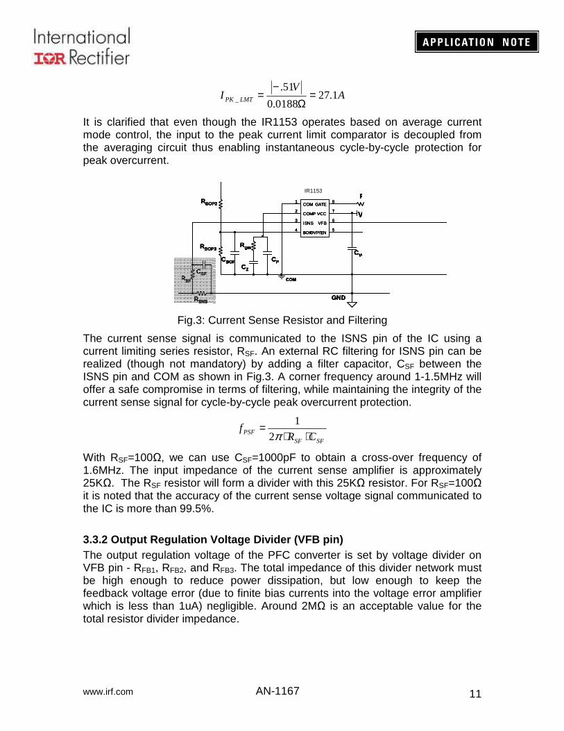
Fig.3: Current Sense Resistor and Filtering
The current sense signal is communicated to the ISNS pin of the IC using a current limiting series resistor, RSF. An external RC filtering for ISNS pin can be realized (though not mandatory) by adding a filter capacitor, CSF between the ISNS pin and COM as shown in Fig.3. A corner frequency around 1-1.5MHz will offer a safe compromise in terms of filtering, while maintaining the integrity of the current sense signal for cycle-by-cycle peak overcurrent protection.
SFSFPSF CR
f⋅⋅
=π2
1
With RSF=100Ω, we can use CSF=1000pF to obtain a cross-over frequency of 1.6MHz. The input impedance of the current sense amplifier is approximately 25KΩ. The RSF resistor will form a divider with this 25KΩ resistor. For RSF=100Ω it is noted that the accuracy of the current sense voltage signal communicated to the IC is more than 99.5%. 3.3.2 Output Regulation Voltage Divider (VFB pin) The output regulation voltage of the PFC converter is set by voltage divider on VFB pin - RFB1, RFB2, and RFB3. The total impedance of this divider network must be high enough to reduce power dissipation, but low enough to keep the feedback voltage error (due to finite bias currents into the voltage error amplifier which is less than 1uA) negligible. Around 2MΩ is an acceptable value for the total resistor divider impedance.
RSNS
RBOP2
RBOP3
RSF
CSFCZ
CPCBOP
Rgm
IR1145
V
GND
CVCC
R
COM
COM1
BOP4
VFB6
VCC7
GATE8
ISNS3
COMP2
OVP/EN5
RSNS
RBOP2
RBOP3
RSF
CSFCZ
CPCBOP
Rgm
IR1145
V
GND
CVCC
R
COM
COM1
BOP4
VFB6
VCC7
GATE8
ISNS3
COMP2
OVP/EN5
RSNS
RBOP2
RBOP3
RSF
CSFCZ
CPCBOP
Rgm
IR1145
V
GND
CVCC
R
COM
COM1
BOP4
VFB6
VCC7
GATE8
ISNS3
COMP2
OVP/EN5
RSNS
RBOP2
RBOP3
RSF
CSFCZ
CPCBOP
Rgm
IR1145
V
GND
CVCC
R
COM
COM1
BOP4
VFB6
VCC7
GATE8
ISNS3
COMP2
OVP/EN5
IR1153
www.irf.com 12
AN-1167
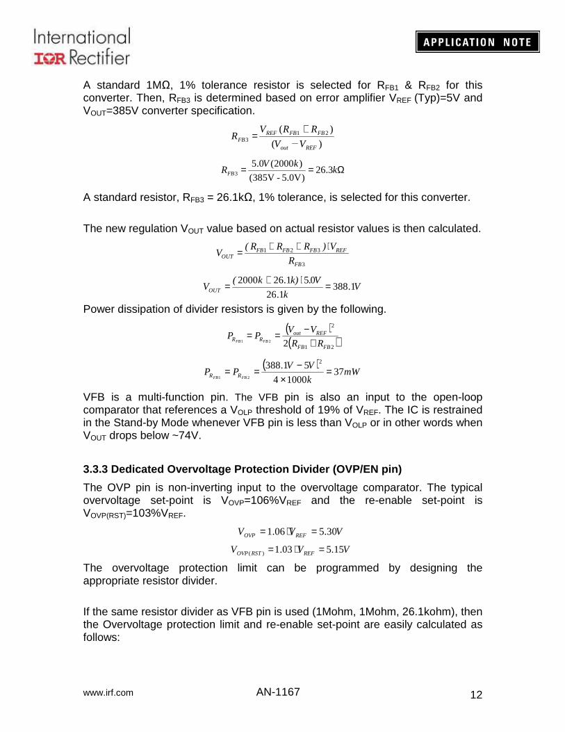
A standard 1MΩ, 1% tolerance resistor is selected for RFB1 & RFB2 for this converter. Then, RFB3 is determined based on error amplifier VREF (Typ)=5V and VOUT=385V converter specification.
)(
)( 213
REFout
FBFBREFFB VV
RRVR
+=
Ω== kkV
RFB 3.26)5.0V-5V38(
)2000(0.53
A standard resistor, RFB3 = 26.1kΩ, 1% tolerance, is selected for this converter. The new regulation VOUT value based on actual resistor values is then calculated.
3
321
FB
REFFBFBFBOUT R
V)RRR(V
⋅++=
Vk
V.k)k(VOUT 1.388
1.26
051.262000 =⋅+=
Power dissipation of divider resistors is given by the following.
( )( )21
2
221
FBFB
REFoutRR RR
VVPP
FBFB +−==
( )mW
k
VVPP
FBFB RR 3710004
51.388 2
21=
×−==
VFB is a multi-function pin. The VFB pin is also an input to the open-loop comparator that references a VOLP threshold of 19% of VREF. The IC is restrained in the Stand-by Mode whenever VFB pin is less than VOLP or in other words when VOUT drops below ~74V.
3.3.3 Dedicated Overvoltage Protection Divider (OVP /EN pin)
The OVP pin is non-inverting input to the overvoltage comparator. The typical overvoltage set-point is VOVP=106%VREF and the re-enable set-point is VOVP(RST)=103%VREF.
VVV REFOVP 30.506.1 =⋅=
VVV REFRSTOVP 15.503.1)( =⋅=
The overvoltage protection limit can be programmed by designing the appropriate resistor divider. If the same resistor divider as VFB pin is used (1Mohm, 1Mohm, 26.1kohm), then the Overvoltage protection limit and re-enable set-point are easily calculated as follows:
www.irf.com 13
AN-1167
VV
VV
OVP
OutOVP
4121.38806.1
06.1
=×=⋅=
VV
VV
RSTOVP
OutRSTOVP
4001.38803.1
03.1
)(
)(
=×=
⋅=
Alternately, if the overvoltage protection limit is required to be VOVP, then the appropriate resistor divider setting can be calculated as follows:
)1.06(
)(06.1 213
REFOVP
OVPOVPREFOVP VV
RRVR
⋅+⋅
=
For example, if VOVP is desired to be 425V (as is the case many times, since the DC bus capacitor is usually rated 450V) and selecting ROVP1=ROVP2=1Mohm, then ROVP3 can be calculated:
)5V1.06425(
)11(506.13 ⋅
+⋅=V
MohmMohmVROVP
kohmROVP 3.253 =
In this design, the IC will enter OVP when VOUT=425V and disable gate output. The gate outputs are re-enabled once the bus voltage drops below the OVP re-enable setpoint, VOVP(RST), which is calculated as follows:
OVPRSTOVP VV ×=06.1
03.1)(
VV RSTOVP 42506.1
03.1)( ×=
VV RSTOVP 413)( =
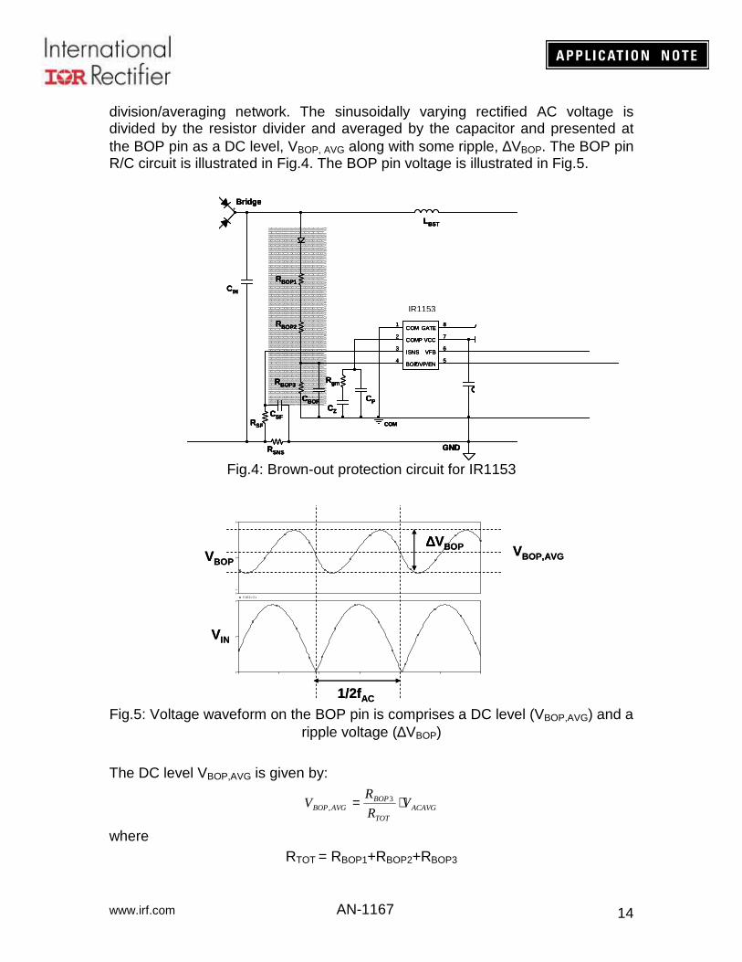
In this converter, for VOVP=425V, then the following resistor divider is selected: ROVP1 = ROVP2 = 1Mohm, ROVP3 = 25.3kohm at 1% tolerance level. Caution: When selecting the overvoltage limit, VOVP and designing the OVP pin resistor divider, it is important to ensure that the resulting re-enable set-point VOVP(RST) does not turn-out to be less than the DC bus regulation voltage, VOUT. Such a design can cause hysteretic oscillations whenever the overvoltage situation is encountered and the system attempts to get back into regulation. It is recommended that the minimum OVP limit be at least equal to 106% of the DC bus regulation voltage i.e. Minimum VOVP≥106%VOUT. This will ensure that VOVP(RST) is always greater than the DC bus regulation voltage VOUT. 3.3.4 Brown-Out Protection R/C Circuit (BOP pin) IR1153 provides brown-out protection based on direct sensing of rectified AC input line. Information about the rectified AC input voltage is communicated to the BOP pin after scaling it down using a resistor divider network and filtering using a capacitor on BOP pin as shown below. This R/C network is essentially a voltage-
www.irf.com 14
AN-1167
RSNS
RBOP1
RBOP2
RBOP3
RSF
CSF
CIN
LBST
CZ
CPCBOP
Rgm
IR1145
GND
Bridge
C
COM
+
COM1
BOP4
VFB6
VCC7
GATE8
ISNS3
COMP2
OVP/EN5
RSNS
RBOP1
RBOP2
RBOP3
RSF
CSF
CIN
LBST
CZ
CPCBOP
Rgm
IR1145
GND
Bridge
C
COM
+
COM1
BOP4
VFB6
VCC7
GATE8
ISNS3
COMP2
OVP/EN5
RSNS
RBOP1
RBOP2
RBOP3
RSF
CSF
CIN
LBST
CZ
CPCBOP
Rgm
IR1145
GND
Bridge
C
COM
+
COM1
BOP4
VFB6
VCC7
GATE8
ISNS3
COMP2
OVP/EN5
RSNS
RBOP1
RBOP2
RBOP3
RSF
CSF
CIN
LBST
CZ
CPCBOP
Rgm
IR1145
GND
Bridge
C
COM
+
COM1
BOP4
VFB6
VCC7
GATE8
ISNS3
COMP2
OVP/EN5
VBOP,AVG
∆∆∆∆VBOP
0V
40V
80VV(R2:2)
750mV
600mV
900mV
SEL>>
1/2fAC
VIN
VBOPVBOP,AVG
∆∆∆∆VBOP
0V
40V
80VV(R2:2)
750mV
600mV
900mV
SEL>>
1/2fAC
VIN
VBOP
division/averaging network. The sinusoidally varying rectified AC voltage is divided by the resistor divider and averaged by the capacitor and presented at the BOP pin as a DC level, VBOP, AVG along with some ripple, ∆VBOP. The BOP pin R/C circuit is illustrated in Fig.4. The BOP pin voltage is illustrated in Fig.5.
Fig.4: Brown-out protection circuit for IR1153 Fig.5: Voltage waveform on the BOP pin is comprises a DC level (VBOP,AVG) and a
ripple voltage (∆VBOP) The DC level VBOP,AVG is given by:
ACAVGTOT
BOPAVGBOP V
R
RV ⋅= 3
,
where RTOT = RBOP1+RBOP2+RBOP3
IR1153
www.irf.com 15
AN-1167
)(, 22
RMSINAVGAC VV ⋅=π
Hence:
)(3
, 22
RMSINTOT
BOPAVGBOP V
R
RV ⋅⋅=
π
Thus VBOP,AVG depends only on the resistor divider and the AC input voltage.
The ripple ∆VBOP is given by the transfer function represented by the resistor divider and the capacitor:
TOT
BOPBOPBOPBOP
TOT
BOP
PKAC
BOP
R
RRRsC
R
R
V
VsT
321
3
,)(
1
1)(
+⋅+
⋅=∆
=
Thus:
2
3)(
)(1
12
O
TOT
BOPRMSINBOP R
RVV
ωω+
⋅⋅⋅=∆
where: )2(2 ACf⋅⋅= πω
BOPBOPBOPBOP
TOTO CRRR
R
⋅⋅+=
321 )(ω
∆VBOP magnitude is related to CBOP – bigger the capacitor, smaller the ripple. During start-up, the IC is held in Stand-by mode when the BOP pin voltage, VBOP is less than VBOP(EN)=1.56V. Next, when the AC voltage is applied and the BOP pin voltage exceeds this threshold, the IC enters normal operation (assuming all other conditions for normal operation are satisfied). If it is assumed that the system is starting under no load, then the rectified AC voltage is essentially a DC voltage and the BOP pin voltage is also DC.
)(3
,3 2 RMSIN
TOT
BOPPKAC
TOT
BOPBOP V
R
RV
R
RV ⋅⋅=⋅=
Under this condition, the AC voltage at which the IC becomes operational is given by:
VVR
RRMSONIN
TOT
BOP 56.12 )(,3 >⋅⋅
However, if the system is starting up under a loaded condition, then the rectified AC voltage is a varying sinusoidal function. In this case, the BOP pin voltage is as described before (DC level + superimposed ripple). In this case, the IC becomes operational when the maxima of VBOP exceeds VBOP(EN)=1.56V.
VBOP,MAX = VBOP,AVG + ∆VBOP /2 > 1.56V
www.irf.com 16
AN-1167
Hence the exact AC voltage at which the IC becomes operational depends on the load condition at start-up. CBOP must be big enough to ensure that ∆VBOP is greater than the BOP hysteresis (1.56-0.76=0.8V) at the required minimum AC input voltage, should the system start-up under a loaded condition. Once the IC becomes operational and starts boosting the DC voltage, then the rectified AC voltage will show sinusoidal variation. Subsequently, if the AC voltage is reduced then VBOP,AVG & ∆VBOP both decrease in magnitude. When the minima of the BOP pin voltage encounters the Brown-out trip threshold VBOP=0.76V then the IC enters brown-out fault mode.
VBOP,MIN = VBOP,AVG - ∆VBOP /2 When a Brown-out fault is encountered, the gate pulse is immediately terminated, the COMP pin is actively discharged, ICC current consumption falls to a few milli-amperes and the BOP pin voltage has to exceed VBOP,EN once again for the IC to restart. The condition at which IC enters Brown-Out fault is then given by:
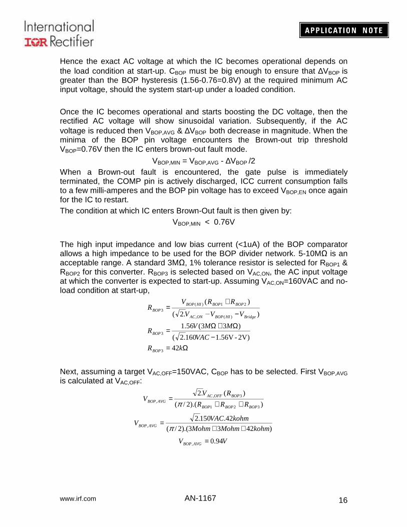
VBOP,MIN < 0.76V The high input impedance and low bias current (<1uA) of the BOP comparator allows a high impedance to be used for the BOP divider network. 5-10MΩ is an acceptable range. A standard 3MΩ, 1% tolerance resistor is selected for RBOP1 & RBOP2 for this converter. RBOP3 is selected based on VAC,ON, the AC input voltage at which the converter is expected to start-up. Assuming VAC,ON=160VAC and no-load condition at start-up,
Ω=−
Ω+Ω=
−
+=
kR
VAC
MMVR
VVV
RRVR
BOP
BOP
BridgeHIBOPONAC
BOPBOPHIBOP
BOP
42
)2V-1.56V160.2(
)33(56.1
).2(
)(
3
3
)(,
21)(3
Next, assuming a target VAC,OFF=150VAC, CBOP has to be selected. First VBOP,AVG is calculated at VAC,OFF:
)).(2/(
)(.2
321
3,,
BOPBOPBOP
BOPOFFACAVGBOP RRR
RVV
++=
π
)4233).(2/(
42.150.2, kohmMohmMohm
kohmVACV AVGBOP ++
=π
VV AVGBOP 94.0, =
www.irf.com 17
AN-1167
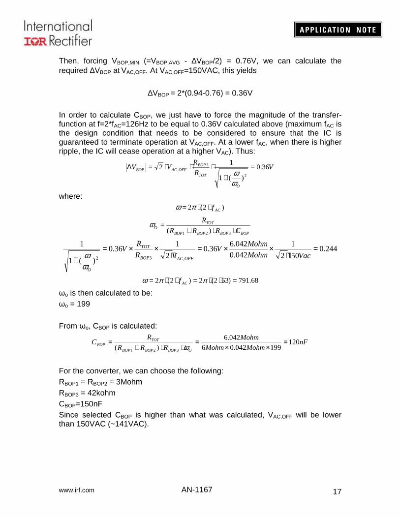
Then, forcing VBOP,MIN (=VBOP,AVG - ∆VBOP/2) = 0.76V, we can calculate the required ∆VBOP at VAC,OFF. At VAC,OFF=150VAC, this yields
∆VBOP = 2*(0.94-0.76) = 0.36V In order to calculate CBOP, we just have to force the magnitude of the transfer-function at f=2*fAC=126Hz to be equal to 0.36V calculated above (maximum fAC is the design condition that needs to be considered to ensure that the IC is guaranteed to terminate operation at VAC,OFF. At a lower fAC, when there is higher ripple, the IC will cease operation at a higher VAC). Thus:
VR
RVV
O
TOT
BOPOFFACBOP 36.0
)(1
12
2
3, =
+⋅⋅⋅=∆
ωω
where: )2(2 ACf⋅⋅= πω
BOPBOPBOPBOP
TOTO CRRR
R
⋅⋅+=
321 )(ω
244.01502
1
042.0
042.636.0
2
136.0
)(1
1
,32
=⋅
××=⋅
××=+ VacMohm
MohmV
VR
RV
OFFACBOP
TOT
Oωω
68.791)632(2)2(2 =⋅⋅=⋅⋅= ππω ACf
ωo is then calculated to be: ωo = 199 From ωo, CBOP is calculated:
nFMohmMohm
Mohm
RRR
RC
OBOPBOPBOP
TOTBOP 120
199042.06
042.6
)( 321
=××
=⋅⋅+
=ω
For the converter, we can choose the following: RBOP1 = RBOP2 = 3Mohm RBOP3 = 42kohm CBOP=150nF Since selected CBOP is higher than what was calculated, VAC,OFF will be lower than 150VAC (~141VAC).
www.irf.com 18
AN-1167
vREF
vFB
Output DividerH1(s)
Error Amplifier +Compensator
H2(s)
∆ vm OCC PFCModulator
H3(s)
iL PlantG(s)
vINvOUT
+
_vREF
vFB
Output DividerH1(s)
Error Amplifier +Compensator
H2(s)
∆ vm OCC PFCModulator
H3(s)
iL PlantG(s)
vINvOUT
vREF
vFB
Output DividerH1(s)
Error Amplifier +Compensator
H2(s)
∆ vm OCC PFCModulator
H3(s)
iL PlantG(s)
vINvOUT
+
_
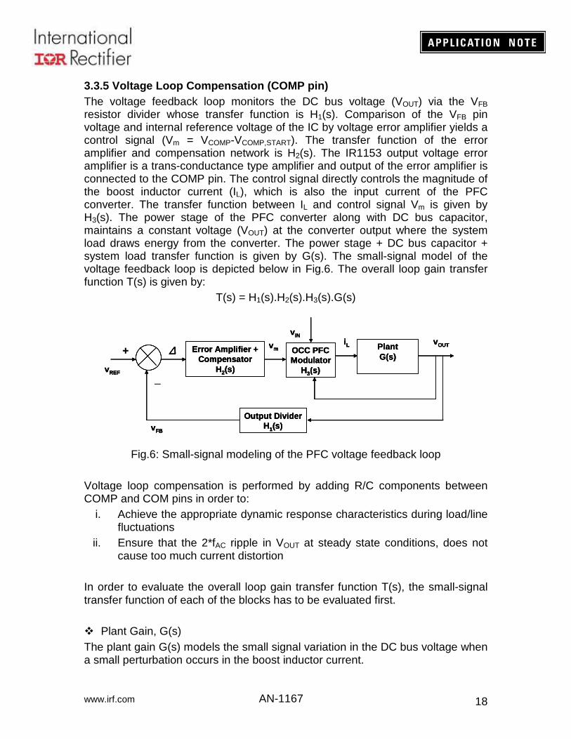
3.3.5 Voltage Loop Compensation (COMP pin) The voltage feedback loop monitors the DC bus voltage (VOUT) via the VFB resistor divider whose transfer function is H1(s). Comparison of the VFB pin voltage and internal reference voltage of the IC by voltage error amplifier yields a control signal (Vm = VCOMP-VCOMP,START). The transfer function of the error amplifier and compensation network is H2(s). The IR1153 output voltage error amplifier is a trans-conductance type amplifier and output of the error amplifier is connected to the COMP pin. The control signal directly controls the magnitude of the boost inductor current (IL), which is also the input current of the PFC converter. The transfer function between IL and control signal Vm is given by H3(s). The power stage of the PFC converter along with DC bus capacitor, maintains a constant voltage (VOUT) at the converter output where the system load draws energy from the converter. The power stage + DC bus capacitor + system load transfer function is given by G(s). The small-signal model of the voltage feedback loop is depicted below in Fig.6. The overall loop gain transfer function T(s) is given by:
T(s) = H1(s).H2(s).H3(s).G(s)
Fig.6: Small-signal modeling of the PFC voltage feedback loop Voltage loop compensation is performed by adding R/C components between COMP and COM pins in order to:
i. Achieve the appropriate dynamic response characteristics during load/line fluctuations
ii. Ensure that the 2*fAC ripple in VOUT at steady state conditions, does not cause too much current distortion
In order to evaluate the overall loop gain transfer function T(s), the small-signal transfer function of each of the blocks has to be evaluated first. Plant Gain, G(s) The plant gain G(s) models the small signal variation in the DC bus voltage when a small perturbation occurs in the boost inductor current.
www.irf.com 19
AN-1167
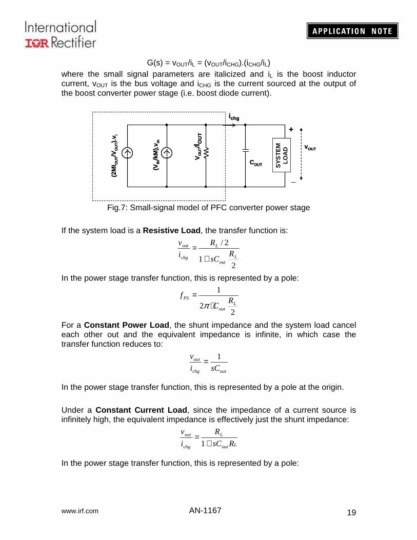
G(s) = vOUT/iL = (vOUT/iCHG).(iCHG/iL) where the small signal parameters are italicized and iL is the boost inductor current, vOUT is the bus voltage and iCHG is the current sourced at the output of the boost converter power stage (i.e. boost diode current).
Fig.7: Small-signal model of PFC converter power stage If the system load is a Resistive Load , the transfer function is:
21
2/
Lout
L
chg
out
RsC
R
i
v
+=
In the power stage transfer function, this is represented by a pole:
22
1
Lout
PS RC
f⋅
=π
For a Constant Power Load , the shunt impedance and the system load cancel each other out and the equivalent impedance is infinite, in which case the transfer function reduces to:
outchg
out
sCi
v 1=
In the power stage transfer function, this is represented by a pole at the origin. Under a Constant Current Load , since the impedance of a current source is infinitely high, the equivalent impedance is effectively just the shunt impedance:
Lout
L
chg
out
RsC
R
i
v
+=
1
In the power stage transfer function, this is represented by a pole:
COUT RL
(2M
I OU
T/V
OU
T).. ..v
i
(VIN
/kM
) .. ..vm
vOUT
VO
UT/I O
UT
ichg
+
_
SY
STE
MLO
AD
COUT RL
(2M
I OU
T/V
OU
T).. ..v
i
(VIN
/kM
) .. ..vm
vOUT
VO
UT/I O
UT
ichg
+
_
SY
STE
MLO
AD
www.irf.com 20
AN-1167
LoutPS RC
f⋅
=π2
1
Next (iCHG/iL) transfer function has to be evaluated. Assuming 100% efficiency, recognize that:
VIN.IL = VOUTIOUT IOUT is same as the DC component of the boost diode current (ICHG). Hence
VIN.IL = VOUTICHG Applying linearization and small-signal analysis, for a given DC operating point defined by VIN & VOUT yields the relationship between iCHG & iL:
iCHG/iL = VIN/VOUT
Assuming a resistive load, the overall power stage transfer function can now be written as:
21
2/)(
Lout
L
OUT
IN
RsC
R
V
VsG
+×=
OCC PFC Modulator, H3(s) In order to derive iL/vm, the One Cycle Control PWM modulator control law is employed:
)(dM
viRG m
LSDC =⋅⋅
where M(d) = VOUT/VIN for a given DC operating point defined by the DC bus voltage VOUT and RMS input voltage VIN. This ultimately yields
DCSOUT
in
m
L
GRV
V
v
isH ==)(3
Output voltage sensor Resistor-Divider, H1(s) The output divider scales the output voltage to be compared with the reference voltage in the error amplifier. Therefore:
3
321 )(
FB
REFFBFBFBOUT R
VRRRV
++=
OUT
REF
V
VsH =)(1
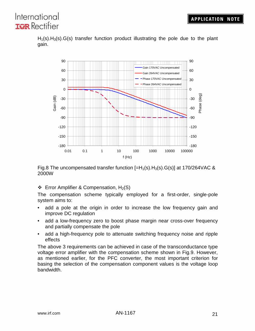
The uncompensated loop gain and phase is shown in Fig.8 for 170-264VAC at 2000W load condition (assuming resistive load). This is simply the
www.irf.com 21
AN-1167
H1(s).H3(s).G(s) transfer function product illustrating the pole due to the plant gain.
Fig.8 The uncompensated transfer function [=H1(s).H3(s).G(s)] at 170/264VAC & 2000W Error Amplifier & Compensation, H2(S) The compensation scheme typically employed for a first-order, single-pole system aims to:
• add a pole at the origin in order to increase the low frequency gain and improve DC regulation
• add a low-frequency zero to boost phase margin near cross-over frequency and partially compensate the pole
• add a high-frequency pole to attenuate switching frequency noise and ripple effects
The above 3 requirements can be achieved in case of the transconductance type voltage error amplifier with the compensation scheme shown in Fig.9. However, as mentioned earlier, for the PFC converter, the most important criterion for basing the selection of the compensation component values is the voltage loop bandwidth.
-180
-150
-120
-90
-60
-30
0
30
60
90
0.01 0.1 1 10 100 1000 10000 100000
f (Hz)
Gai
n (d
B)
-180
-150
-120
-90
-60
-30
0
30
60
90
Pha
se (
deg)
Gain 170VAC Uncompensated
Gain 264VAC Uncompensated
Phase 170VAC Uncompensated
Phase 264VAC Uncompensated
www.irf.com 22
AN-1167
-180
-150
-120
-90
-60
-30
0
30
60
90
0.01 0.1 1 10 100 1000 10000 100000
f (Hz)
Gai
n (d
B)
-180
-150
-120
-90
-60
-30
0
30
60
90
Pha
se (
deg)
EA Gain
EA Phase
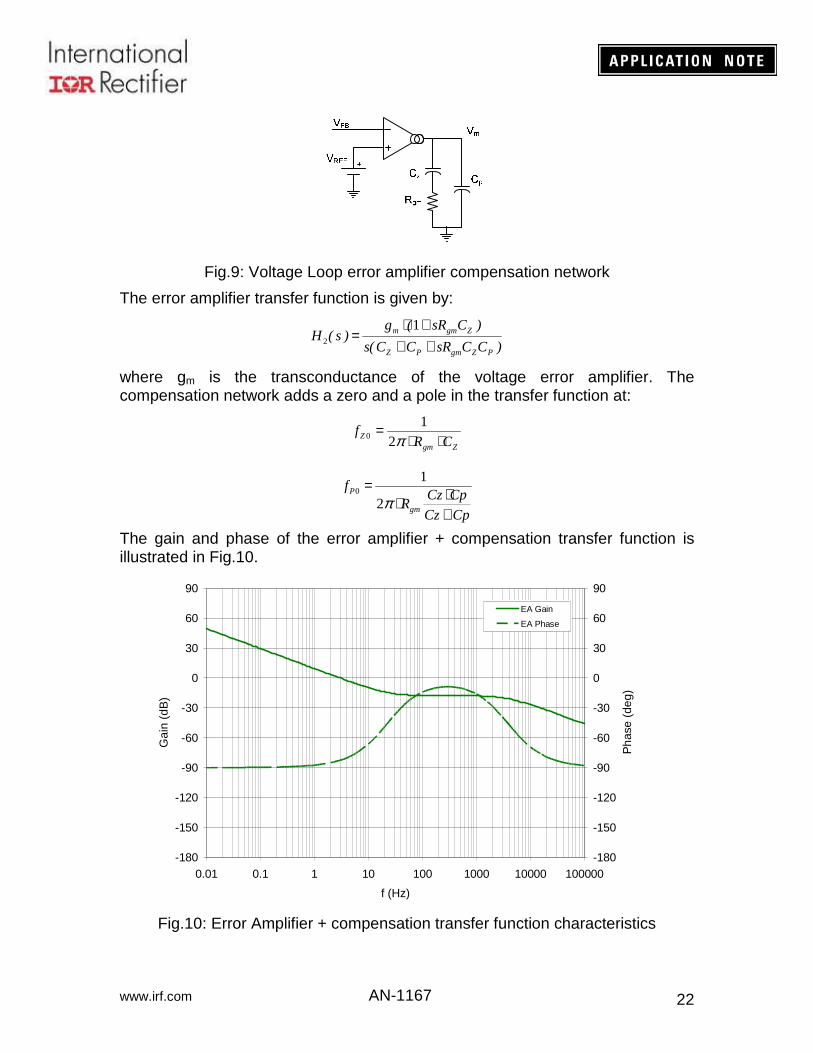
Fig.9: Voltage Loop error amplifier compensation network
The error amplifier transfer function is given by:
)CCsRCC(s
)CsR(g)s(H
PZgmPZ
Zgmm
+++⋅
=1
2
where gm is the transconductance of the voltage error amplifier. The compensation network adds a zero and a pole in the transfer function at:
ZgmZ CR
f⋅⋅
=π2
10
CpCz
CpCzR
f
gm
P
+⋅⋅
=π2
10
The gain and phase of the error amplifier + compensation transfer function is illustrated in Fig.10.
Fig.10: Error Amplifier + compensation transfer function characteristics
www.irf.com 23
AN-1167
Voltage Loop Compensation procedure Step 1: Choose Cz based on soft-start time: A soft-start time of 300ms is selected. The soft-start time represents the time needed by the controller to ramp VCOMP from zero to the maximum value. In other words, even when current demand at start-up is highest (lowest line and highest load start-up situation), the system will take no more than 300ms to achieve near-regulation.
)()( MINV
itC
EFFCOMP
OVEASSZ
⋅=
iOVEA and VCOMP(EFF)(MIN) are taken from the datasheet.
FV
AmsCZ µµ
8.27.4
44300 =×=
Step 2: Choose Rgm to ensure that H1(s).H2(s) attenuation at 2xfAC frequency is small enough to avoid current distortion: The amount of 2xfAC ripple on the output capacitor is calculated first. The minimum fAC of 47Hz is considered here, since the ripple is the maximum at the lowest AC frequency. The peak-to-zero ripple VOPK is given by:
outOAC
MAXinOPK VCf
PV
⋅⋅⋅⋅=
22,
π
VV
VF
WV
OPK
OPK
8.6
38514104722
2173
=⋅⋅⋅⋅
=µπ
The peak-to-peak ripple in VOUT is 2xVOPK. This ripple in VOUT is reflected in the VCOMP voltage based on the attenuation provided by the resistor divider and error amplifier compensation network combined i.e. H1(s).H2(s) at 2xfAC. The ripple in VCOMP i.e. ∆VCOMP has to be small compared with the value of the error amplifier output voltage swing (VCOMP,EFF). Typical values for ∆VCOMP/VCOMP range from 0.5% to 1%. 0.5% is recommended if current shaping has to be excellent while 1% is recommended for higher phase margin and low-oscillation response to load steps. 0.5% attenuation demands a (GVA) of:
OPK
EFFCOMPVA V
VG
⋅⋅
=2
005.0)(
dBGV
VG
VA
VA
2.55
00173.08.62
005.07.4
−=
=⋅
⋅=
www.irf.com 24
AN-1167
This is the required attenuation in H1(s).H2(s) at 2xfAC frequency. H1(s), given by VREF/VOUT, is next calculated:
dBV
VH 7.37013.0
385
51 −===
The required attenuation from H2(s) alone at 2x47Hz is then given by:
dBHGVA 5.171 −=−
Since the error amplifier pole will be set at a much higher frequency than 2xfAC (and consequently Cz >> Cp), the error amplifier transfer function at 2xfAC can be approximated to:
Z
Zgmm
sC
)CsR(g)s(H
+⋅≅
12
Since CZ has already been determined, only Rgm needs to be calculated by forcing:
133.05.17)2( 12 =−=−=⋅ dBHGfjH VAACπ 22
1
22
1
⋅⋅⋅−
−=ZACm
VAgm Cfg
HGR
π
Substituting fAC=47Hz, gm=49µS, CZ=2.8µF yields
Ω= kRgm 65.2
The location of the zero in the compensation scheme can now be estimated:
fz = 1/(2*π*Rgm.Cz) = 1/(2*3.14*2.65kohm*2.8µF) = 21.4Hz The location of the pole in the power stage transfer function (assuming a resistive load) is:
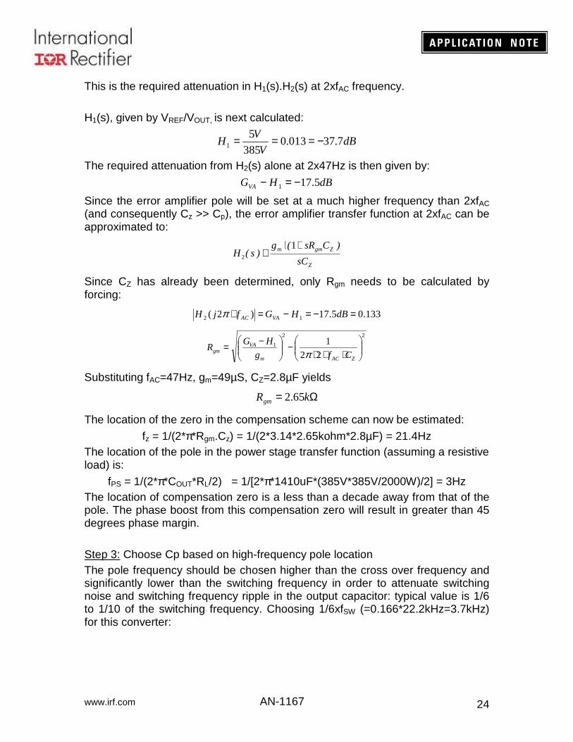
fPS = 1/(2*π*COUT*RL/2) = 1/[2*π*1410uF*(385V*385V/2000W)/2] = 3Hz The location of compensation zero is a less than a decade away from that of the pole. The phase boost from this compensation zero will result in greater than 45 degrees phase margin. Step 3: Choose Cp based on high-frequency pole location The pole frequency should be chosen higher than the cross over frequency and significantly lower than the switching frequency in order to attenuate switching noise and switching frequency ripple in the output capacitor: typical value is 1/6 to 1/10 of the switching frequency. Choosing 1/6xfSW (=0.166*22.2kHz=3.7kHz) for this converter:
www.irf.com 25
AN-1167
-180
-150
-120
-90
-60
-30
0
30
60
90
0.01 0.1 1 10 100 1000 10000 100000
f (Hz)
Gai
n (d
B)
-180
-150
-120
-90
-60
-30
0
30
60
90
Pha
se (
deg)
Gain 264VAC Uncompensated
Gain 264VAC Compensated
EA Gain
EA Phase
Phase 264VAC Uncompensated
Phase 264VAC Compensated
-180
-150
-120
-90
-60
-30
0
30
60
90
0.01 0.1 1 10 100 1000 10000 100000
f (Hz)
Gai
n (d
B)
-180
-150
-120
-90
-60
-30
0
30
60
90
Pha
se (
deg)
Gain 170VAC Uncompensated
Gain 170VAC Compensated
EA Gain
Phase 170VAC Uncompensated
Phase 170VAC Compensated
EA Phase
CpRCpCz
CpCzR
fgm
gm
P ⋅⋅≅
+⋅⋅
=ππ 2
1
2
10
nFkHzk
C p 16166.02.2265.22
1 =⋅⋅Ω⋅
=π
Step 4: Estimate bandwidth & phase margin The voltage loop response for 170VAC and 264VAC is plotted at full load condition in Fig.11. At 170VAC/2000W the cross-over frequency is 2.1Hz and phase margin is 61°. At 264VAC/2000W the cross-over frequency is 3.9Hz and phase margin is 48°. This compensation scheme ensures that PFC converter has cross-over frequency less than ½xfAC, low magnitude of 2xfAC ripple on VCOMP and adequate phase margin. It satisfies all the requirements of the design.
Fig.11: Overall Loop Gain at 170/264VAC & 2000W
www.irf.com 26
AN-1167
-180
-150
-120
-90
-60
-30
0
30
60
90
0.01 0.1 1 10 100 1000 10000 100000
f (Hz)
Gai
n (d
B)
-180
-150
-120
-90
-60
-30
0
30
60
90P
hase
(de
g)
Gain 264VAC Uncompensated
Gain 264VAC Compensated
EA Gain
EA Phase
Phase 264VAC Uncompensated
Phase 264VAC Compensated
-180
-150
-120
-90
-60
-30
0
30
60
90
0.01 0.1 1 10 100 1000 10000 100000
f (Hz)
Gai
n (d
B)
-180
-150
-120
-90
-60
-30
0
30
60
90
Pha
se (
deg)
Gain 170VAC Uncompensated
Gain 170VAC Compensated
EA Gain
Phase 170VAC Uncompensated
Phase 170VAC Compensated
EA Phase
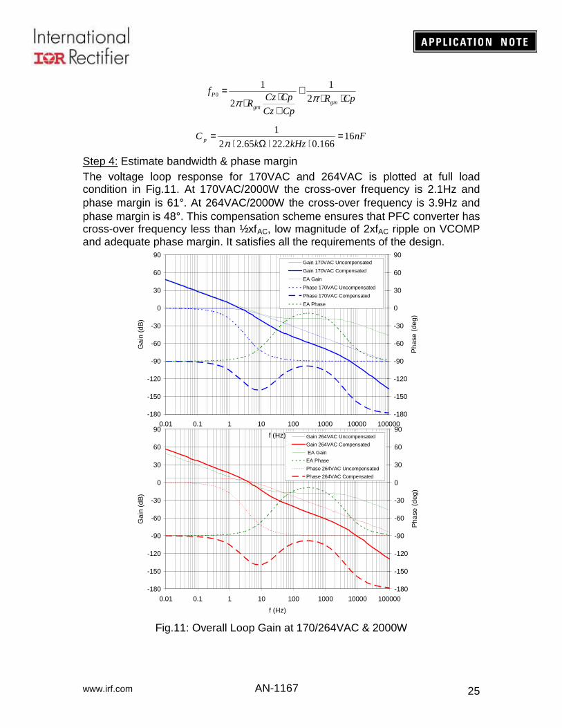
It is instructive to study the compensation for slightly different system designs: Case1: What happens if the system is designed for a much smaller start-up time? For example, if the soft-start time is decreased to 100ms (1/3x reduction), then re-calculating according to the procedure described above yields Cz=0.93uF, Rgm=2kohm, Cp=21nF. The cross-over frequency and phase margin are 4.3Hz & 38° at 170VAC and 7.1Hz and 28° at 264VAC as seen in Fig.12 below. Due to the lower Cz capacitor, the low frequency gain is increased and hence the band-width is increased. But the location of the zero is further away from the power stage pole, so the phase margin will be reduced resulting in a more oscillatory response to VOUT when there is a load step. Fig.12: Overall Loop Gain at 170/264VAC, 2000W (reduced start-up time causes lower phase margin)
www.irf.com 27
AN-1167
Case2: What happens if the system is designed for a much smaller hold-up time? For example, if the bus capacitor is reduced to 2x470uF=940uF. Running the calculations again
VV
VF
WV
OPK
OPK
2.10
3859404722
2173
=⋅⋅⋅⋅
=µπ
dBGV
VG
VA
VA
7.58
00115.02.102
005.07.4
−=
=⋅
⋅=
The required attenuation from H2(s) alone at 2x47Hz is then given by:
dBHGVA 211 −=−
Recalculating the compensation components according to the procedure above: Assuming a start-up time of 100ms yields Cz=0.93uF. Next, Rgm is determined using:
22
1
22
1
⋅⋅⋅−
−=ZACm
VAgm Cfg
HGR
π
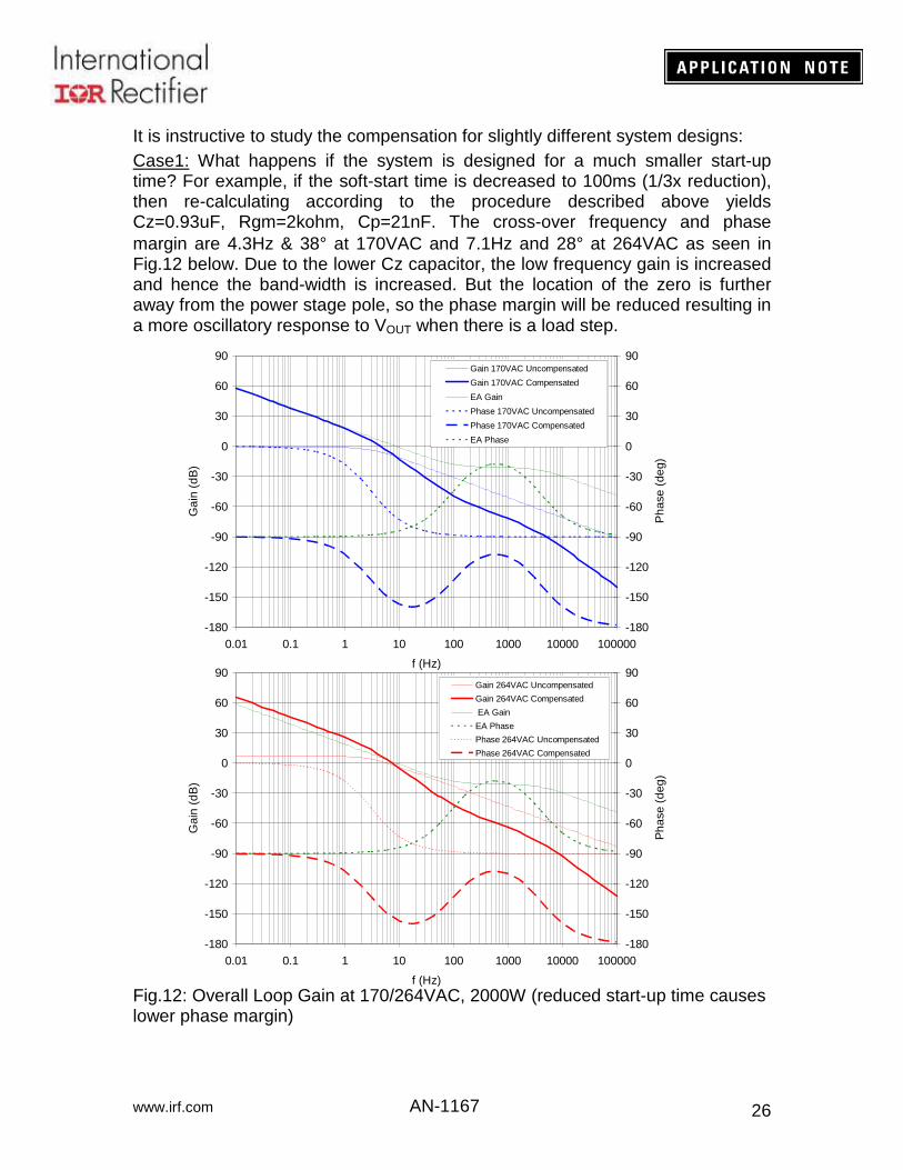
If the math is performed, it will be seen that the Rgm calculation using above equation will yield an imaginary value. What this means is that the attenuation provided by the error amplifier’s origin pole is not quite enough to achieve the 0.5% 2xfAC ripple requirement in VCOMP for current distortion considerations [The 2xfAC ripple in VCOMP pin must be restricted to less than 0.5% (∆VCOMP/VCOMP) in order to avoid any noticeable current distortion]. In this case, there is no choice but to decrease the low frequency gain of the error amplifier H2(s), by increasing Cz capacitor. However this will result in higher start-up time. A minimum start-up time of 111ms (corresponding to Cz=1.04uF) is required to yield a real value for Rgm in order to meet the VCOMP 2xfAC ripple requirement. Recalculating the compensation for soft-start time=111ms yields: Cz=1.04uF, Rgm=800ohms and Cp=54nF. The loop response plots can now be generated (Fig.13) and studied. The cross-over frequency and phase margin are 4.6Hz & 46° at 170VAC and 7.9Hz and 32° at 264VAC as seen in Fig.13 below.
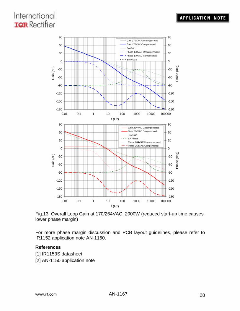
www.irf.com 28
AN-1167
-180
-150
-120
-90
-60
-30
0
30
60
90
0.01 0.1 1 10 100 1000 10000 100000
f (Hz)
Gai
n (d
B)
-180
-150
-120
-90
-60
-30
0
30
60
90
Pha
se (
deg)
Gain 264VAC Uncompensated
Gain 264VAC Compensated
EA Gain
EA Phase
Phase 264VAC Uncompensated
Phase 264VAC Compensated
-180
-150
-120
-90
-60
-30
0
30
60
90
0.01 0.1 1 10 100 1000 10000 100000
f (Hz)
Gai
n (d
B)
-180
-150
-120
-90
-60
-30
0
30
60
90
Pha
se (
deg)
Gain 170VAC Uncompensated
Gain 170VAC Compensated
EA Gain
Phase 170VAC Uncompensated
Phase 170VAC Compensated
EA Phase
Fig.13: Overall Loop Gain at 170/264VAC, 2000W (reduced start-up time causes lower phase margin) For more phase margin discussion and PCB layout guidelines, please refer to IR1152 application note AN-1150.
References [1] IR1153S datasheet [2] AN-1150 application note