Embed Size (px)
Citation preview

GK21-0263-002/23/99
PowerPC 740 TM
PowerPC 750 TM
RISC MicroprocessorUser’s Manual

© IBM1999Portions hereof © IMotorola Inc. 1999. All rights reserved.
This document contains information on a new product under development by IBM. IBM reserve the right to change or discontinue this product withoutnotice. Information in this document is provided solely to enable system and software implementers to use PowerPC microprocessors. There are noexpress or implied copyright or patent licenses granted hereunder by IBM to design, modify the design of, or fabricate circuits based on the informationin this document.
The PowerPC 750 microprocessor embodies the intellectual property of IBM. However, IBM does not assume any responsibility or liability as to anyaspects of the performance, operation, or other attributes of the microprocessor as marketed by the other party or by any third party. IBM has neitherassumed, created, or granted hereby any right or authority to any third party to assume or create any express or implied obligations on its behalf.Information such as data sheets, as well as sales terms and conditions such as prices, schedules, and support, for the product may vary as betweenparties selling the product. Accordingly, customers wishing to learn more information about the products as marketed by a given party should contact thatparty.
IBM reserves the right to modify this manual and/or any of the products as described herein without further notice. NOTHING IN THIS MANUAL, NORIN ANY OF THE ERRATA SHEETS, DATA SHEETS, AND OTHER SUPPORTING DOCUMENTATION, SHALL BE INTERPRETED AS THECONVEYANCE BY IBM AN EXPRESS WARRANTY OF ANY KIND OR IMPLIED WARRANTY, REPRESENTATION, OR GUARANTEE REGARDINGTHE MERCHANTABILITY OR FITNESS OF THE PRODUCTS FOR ANY PARTICULAR PURPOSE . IBM does not assume any liability or obligation fordamages of any kind arising out of the application or use of these materials. Any warranty or other obligations as to the products described herein shallbe undertaken solely by the marketing party to the customer, under a separate sale agreement between the marketing party and the customer. In theabsence of such an agreement, no liability is assumed by IBM or the marketing party for any damages, actual or otherwise.
“Typical” parameters can and do vary in different applications. All operating parameters, including “Typicals,” must be validated for each customerapplication by customer’s technical experts. IBM does not convey any license under their respective intellectual property rights nor the rights of others.IBM makes no claim, warranty, or representation, express or implied, that the products described in this manual are designed, intended, or authorized foruse as components in systems intended for surgical implant into the body, or other applications intended to support or sustain life, or for any otherapplication in which the failure of the product could create a situation where personal injury or death may occur. Should customer purchase or use theproducts for any such unintended or unauthorized application, customer shall indemnify and hold IBM and its respective officers, employees, subsidiaries,affiliates, and distributors harmless against all claims, costs, damages, and expenses, and reasonable attorney fees arising out of, directly or indirectly,any claim of personal injury or death associated with such unintended or unauthorized use, even if such claim alleges that IBM was negligent regardingthe design or manufacture of the part.
IBM and IBM logo are registered trademarks, and IBM Microelectronics is a trademark of International Business Machines Corp. The PowerPC name,PowerPC logotype, PowerPC 740, and PowerPC 750 are trademarks of International Business Machines Corp. International Business Machines Corp.is an Equal Opportunity/Affirmative Action Employer.
International Business Machines Corporation:IBM Microelectronics Division1580 Route 52, Bldg. 504Hopewell Junction, NY 12533-6531;
WWW Addresses :http://www.chips.ibm.com/http://www.ibm.com/

1
2
3
4
5
6
8
7
A
B
IND
GLO
9
10
11
PowerPC 740/PowerPC 750 Overview
Processor Programming Model
L1 Instruction and Data Cache Operation
Exceptions
Memory Management
Instruction Timing
Signal Descriptions
Bus Interface Operation
L2 Cache Interface Operation
Power and Thermal Management
Performance Monitor
PowerPC Instruction Set Listings
Instructions Not Implemented
Glossary of Terms and Abbreviations
Index

. xxvii
. xxvii. xxviii....xxx...xxxxxiv
... 1-1..... 1-4.... 1-4... 1-7... 1-8... 1-8... 1-9.. 1-10. 1-101-101-11. 1-111-12.. 1-12. 1-141-15.. 1-16. 1-18.. 1-19. 1-19.. 1-21.. 1-26.. 1-27.. 1-28.. 1-29.. 1-29.. 1-29. 1-29. 1-29. 1-31.. 1-32. 1-33. 1-33
ParagraphNumber Title Page
Number
Contents
Preface
Audience ..........................................................................................................Organization.....................................................................................................Suggested Reading..........................................................................................Conventions .....................................................................................................Acronyms and Abbreviations ...........................................................................Terminology Conventions ............................................................................... x
Chapter 1PowerPC 740/PowerPC 750 Overview
1.1 PowerPC 750 Microprocessor Overview..........................................................1.2 PowerPC 750 Microprocessor Features..........................................................1.2.1 Overview of the PowerPC 750 Microprocessor Features............................1.2.2 Instruction Flow............................................................................................1.2.2.1 Instruction Queue and Dispatch Unit .......................................................1.2.2.2 Branch Processing Unit (BPU).................................................................1.2.2.3 Completion Unit .......................................................................................1.2.2.4 Independent Execution Units...................................................................1.2.2.4.1 Integer Units (IUs)................................................................................1.2.2.4.2 Floating-Point Unit (FPU) .....................................................................1.2.2.4.3 Load/Store Unit (LSU) ..........................................................................1.2.2.4.4 System Register Unit (SRU).................................................................1.2.3 Memory Management Units (MMUs)...........................................................1.2.4 On-Chip Instruction and Data Caches .........................................................1.2.5 L2 Cache Implementation (Not Supported in the PowerPC 740) ................1.2.6 System Interface/Bus Interface Unit (BIU) ...................................................1.2.7 Signals..........................................................................................................1.2.8 Signal Configuration.....................................................................................1.2.9 Clocking.......................................................................................................1.3 PowerPC 750 Microprocessor: Implementation...............................................1.4 PowerPC Registers and Programming Model .................................................1.5 Instruction Set ..................................................................................................1.5.1 PowerPC Instruction Set..............................................................................1.5.2 PowerPC 750 Microprocessor Instruction Set.............................................1.6 On-Chip Cache Implementation ......................................................................1.6.1 PowerPC Cache Model................................................................................1.6.2 PowerPC 750 Microprocessor Cache Implementation................................1.7 Exception Model...............................................................................................1.7.1 PowerPC Exception Model...........................................................................1.7.2 PowerPC 750 Microprocessor Exception Implementation...........................1.8 Memory Management......................................................................................1.8.1 PowerPC Memory Management Model .......................................................1.8.2 PowerPC 750 Microprocessor Memory Management Implementation .......
Contents v

ContentsParagraphNumber Title Page
Number
.1-34
...1-36...1-37..1-38
......2-1
.....2-1.....2-8..2-8....2-9..2-13..2-14-14-15-16-16
.2-162-20..2-20.2-20ess
2-21.2-21..2-24...2-282-28..2-28..2-29..2-29...2-31...2-322-33..2-33..2-33...2-34...2-35..2-35...2-35..2-35
1.9 Instruction Timing .............................................................................................1.10 Power Management .........................................................................................1.11 Thermal Management......................................................................................1.12 Performance Monitor........................................................................................
Chapter 2Programming Model
2.1 The PowerPC 750 Processor Register Set......................................................2.1.1 Register Set..................................................................................................2.1.2 PowerPC 750-Specific Registers.................................................................2.1.2.1 Instruction Address Breakpoint Register (IABR) ......................................2.1.2.2 Hardware Implementation-Dependent Register 0....................................2.1.2.3 Hardware Implementation-Dependent Register 1....................................2.1.2.4 Performance Monitor Registers................................................................2.1.2.4.1 Monitor Mode Control Register 0 (MMCR0)........................................22.1.2.4.2 User Monitor Mode Control Register 0 (UMMCR0) ............................22.1.2.4.3 Monitor Mode Control Register 1 (MMCR1)........................................22.1.2.4.4 User Monitor Mode Control Register 1 (UMMCR1) ............................22.1.2.4.5 Performance Monitor Counter Registers (PMC1–PMC4) ....................2.1.2.4.6 User Performance Monitor Counter Registers (UPMC1–UPMC4).......2.1.2.4.7 Sampled Instruction Address Register (SIA) .......................................2.1.2.4.8 User Sampled Instruction Address Register (USIA).............................2.1.2.4.9 Sampled Data Address Register (SDA) and User Sampled Data Addr
Register (USDA)2-202.1.3 Instruction Cache Throttling Control Register (ICTC) ..................................2.1.4 Thermal Management Registers (THRM1–THRM3) ...................................2.1.5 L2 Cache Control Register (L2CR)..............................................................2.2 Operand Conventions ......................................................................................2.2.1 Floating-Point Execution Models—UISA .....................................................2.2.2 Data Organization in Memory and Data Transfers ......................................2.2.3 Alignment and Misaligned Accesses............................................................2.2.4 Floating-Point Operand ................................................................................2.3 Instruction Set Summary .................................................................................2.3.1 Classes of Instructions.................................................................................2.3.1.1 Definition of Boundedly Undefined...........................................................2.3.1.2 Defined Instruction Class .........................................................................2.3.1.3 Illegal Instruction Class............................................................................2.3.1.4 Reserved Instruction Class ......................................................................2.3.2 Addressing Modes.......................................................................................2.3.2.1 Memory Addressing .................................................................................2.3.2.2 Memory Operands...................................................................................2.3.2.3 Effective Address Calculation..................................................................
vi IBM PowerPC 740 / PowerPC 750 RISC Microprocessor User’s Manual

Contents
ParagraphNumber Title Page
Number
..2-36..2-36.2-36..2-37..2-37.2-38..2-38.2-38..2-39.2-40..2-40.2-412-42-42
.2-43.2-43.2-44.2-44..2-45.2-45...2-46.2-46..2-47..2-48.2-49.2-49..2-50..2-51.2-51.2-53.2-53..2-542-54..2-552-55.2-552-562-562-59.2-60.2-602-612-62
2.3.2.4 Synchronization .......................................................................................2.3.2.4.1 Context Synchronization......................................................................2.3.2.4.2 Execution Synchronization ...................................................................2.3.2.4.3 Instruction-Related Exceptions............................................................2.3.3 Instruction Set Overview..............................................................................2.3.4 PowerPC UISA Instructions .........................................................................2.3.4.1 Integer Instructions ..................................................................................2.3.4.1.1 Integer Arithmetic Instructions .............................................................2.3.4.1.2 Integer Compare Instructions...............................................................2.3.4.1.3 Integer Logical Instructions ..................................................................2.3.4.1.4 Integer Rotate and Shift Instructions ...................................................2.3.4.2 Floating-Point Instructions........................................................................2.3.4.2.1 Floating-Point Arithmetic Instructions ..................................................2.3.4.2.2 Floating-Point Multiply-Add Instructions .............................................22.3.4.2.3 Floating-Point Rounding and Conversion Instructions.........................2.3.4.2.4 Floating-Point Compare Instructions....................................................2.3.4.2.5 Floating-Point Status and Control Register Instructions ......................2.3.4.2.6 Floating-Point Move Instructions .........................................................2.3.4.3 Load and Store Instructions .....................................................................2.3.4.3.1 Self-Modifying Code ............................................................................2.3.4.3.2 Integer Load and Store Address Generation.......................................2.3.4.3.3 Register Indirect Integer Load Instructions ..........................................2.3.4.3.4 Integer Store Instructions.....................................................................2.3.4.3.5 Integer Store Gathering........................................................................2.3.4.3.6 Integer Load and Store with Byte-Reverse Instructions .......................2.3.4.3.7 Integer Load and Store Multiple Instructions .......................................2.3.4.3.8 Integer Load and Store String Instructions ..........................................2.3.4.3.9 Floating-Point Load and Store Address Generation ............................2.3.4.3.10 Floating-Point Store Instructions ..........................................................2.3.4.4 Branch and Flow Control Instructions ......................................................2.3.4.4.1 Branch Instruction Address Calculation ...............................................2.3.4.4.2 Branch Instructions ..............................................................................2.3.4.4.3 Condition Register Logical Instructions ................................................2.3.4.4.4 Trap Instructions ..................................................................................2.3.4.5 System Linkage Instruction—UISA ..........................................................2.3.4.6 Processor Control Instructions—UISA.....................................................2.3.4.6.1 Move to/from Condition Register Instructions ......................................2.3.4.6.2 Move to/from Special-Purpose Register Instructions (UISA) ...............2.3.4.7 Memory Synchronization Instructions—UISA .........................................2.3.5 PowerPC VEA Instructions...........................................................................2.3.5.1 Processor Control Instructions—VEA......................................................2.3.5.2 Memory Synchronization Instructions—VEA...........................................2.3.5.3 Memory Control Instructions—VEA.........................................................
Contents vii

ContentsParagraphNumber Title Page
Number
.2-62
.2-64
..2-65
.2-65.2-652-66.2-66.2-672-67..2-68
.....3-3
....3-4.....3-5..3-6....3-7....3-9....3-10...3-10..3-10....3-11...3-11..3-11...3-13..3-13..3-13..3-13..3-14..3-14.3-14..3-15..3-15
516161777....3-18...3-18
2.3.5.3.1 User-Level Cache Instructions—VEA..................................................2.3.5.4 Optional External Control Instructions .....................................................2.3.6 PowerPC OEA Instructions..........................................................................2.3.6.1 System Linkage Instructions—OEA.........................................................2.3.6.2 Processor Control Instructions—OEA ......................................................2.3.6.3 Memory Control Instructions—OEA.........................................................2.3.6.3.1 Supervisor-Level Cache Management Instruction—(OEA) .................2.3.6.3.2 Segment Register Manipulation Instructions (OEA) ............................2.3.6.3.3 Translation Lookaside Buffer Management Instructions—(OEA)........2.3.7 Recommended Simplified Mnemonics ........................................................
Chapter 3 Instruction and Data Cache Operation
3.1 Data Cache Organization.................................................................................3.2 Instruction Cache Organization........................................................................3.3 Memory and Cache Coherency .......................................................................3.3.1 Memory/Cache Access Attributes (WIMG Bits) ...........................................3.3.2 MEI Protocol ................................................................................................3.3.2.1 MEI Hardware Considerations.................................................................3.3.3 Coherency Precautions in Single Processor Systems.................................3.3.4 Coherency Precautions in Multiprocessor Systems ....................................3.3.5 PowerPC 750-Initiated Load/Store Operations ............................................3.3.5.1 Performed Loads and Stores...................................................................3.3.5.2 Sequential Consistency of Memory Accesses.........................................3.3.5.3 Atomic Memory References ....................................................................3.4 Cache Control ..................................................................................................3.4.1 Cache Control Parameters in HID0..............................................................3.4.1.1 Data Cache Flash Invalidation .................................................................3.4.1.2 Data Cache Enabling/Disabling ...............................................................3.4.1.3 Data Cache Locking .................................................................................3.4.1.4 Instruction Cache Flash Invalidation........................................................3.4.1.5 Instruction Cache Enabling/Disabling.......................................................3.4.1.6 Instruction Cache Locking .......................................................................3.4.2 Cache Control Instructions ...........................................................................3.4.2.1 Data Cache Block Touch (dcbt) and
Data Cache Block Touch for Store (dcbtst) ..........................................3-13.4.2.2 Data Cache Block Zero (dcbz)...................................................................3-3.4.2.3 Data Cache Block Store (dcbst).................................................................3-3.4.2.4 Data Cache Block Flush (dcbf)..................................................................3-3.4.2.5 Data Cache Block Invalidate (dcbi) ...........................................................3-13.4.2.6 Instruction Cache Block Invalidate (icbi) ..................................................3-13.5 Cache Operations............................................................................................3.5.1 Cache Block Replacement/Castout Operations...........................................
viii IBM PowerPC 740 / PowerPC 750 RISC Microprocessor User’s Manual

Contents
ParagraphNumber Title Page
Number
...3-21
.3-213-21..3-223-22...3-22..3-23..3-24...3-25....3-26..3-29..3-31
....4-2
...4-4.....4-7..4-10...4-10.4-11.4-11...4-12.4-12...4-13...4-14...4-15.4-174-18.4-19.4-19.4-19.4-20.4-20..4-204-21..4-21..4-21..4-22.4-22.4-22.4-23..4-25
3.5.2 Cache Flush Operations ..............................................................................3.5.3 Data Cache-Block-Fill Operations................................................................3.5.4 Instruction Cache-Block-Fill Operations .......................................................3.5.5 Data Cache-Block-Push Operation ..............................................................3.5.5.1 Enveloped High-Priority Cache-Block-Push Operation ............................3.6 L1 Caches and 60x Bus Transactions .............................................................3.6.1 Read Operations and the MEI Protocol .......................................................3.6.2 Bus Operations Caused by Cache Control Instructions ...............................3.6.3 Snooping .....................................................................................................3.6.4 Snoop Response to 60x Bus Transactions .................................................3.6.5 Transfer Attributes .......................................................................................3.7 MEI State Transactions ....................................................................................
Chapter 4 Exceptions
4.1 PowerPC 750 Microprocessor Exceptions.......................................................4.2 Exception Recognition and Priorities................................................................4.3 Exception Processing ......................................................................................4.3.1 Enabling and Disabling Exceptions .............................................................4.3.2 Steps for Exception Processing...................................................................4.3.3 Setting MSR[RI] ...........................................................................................4.3.4 Returning from an Exception Handler ..........................................................4.4 Process Switching ...........................................................................................4.5 Exception Definitions........................................................................................4.5.1 System Reset Exception (0x00100) ............................................................4.5.1.1 Soft Reset ................................................................................................4.5.1.2 Hard Reset...............................................................................................4.5.2 Machine Check Exception (0x00200)...........................................................4.5.2.1 Machine Check Exception Enabled (MSR[ME] = 1) ................................4.5.2.2 Checkstop State (MSR[ME] = 0)..............................................................4.5.3 DSI Exception (0x00300) .............................................................................4.5.4 ISI Exception (0x00400) ...............................................................................4.5.5 External Interrupt Exception (0x00500) .......................................................4.5.6 Alignment Exception (0x00600)...................................................................4.5.7 Program Exception (0x00700) .....................................................................4.5.8 Floating-Point Unavailable Exception (0x00800) .........................................4.5.9 Decrementer Exception (0x00900) ..............................................................4.5.10 System Call Exception (0x00C00)...............................................................4.5.11 Trace Exception (0x00D00).........................................................................4.5.12 Floating-Point Assist Exception (0x00E00)..................................................4.5.13 Performance Monitor Interrupt (0x00F00) ...................................................4.5.14 Instruction Address Breakpoint Exception (0x01300)..................................4.5.15 System Management Interrupt (0x01400) ...................................................
Contents ix

ContentsParagraphNumber Title Page
Number
..4-26
...5-2
....5-4
...5-4.....5-9.5-11..5-12.5-12..5-12...5-14.5-16.5-18...5-20..5-21..5-21...5-21...5-22...5-23...5-23...5-25.5-25..5-25.5-27...5-28....5-30....5-34....5-34
....6-1...6-3....6-7....6-8.6-11..6-11...6-11...6-14
4.5.16 Thermal Management Interrupt Exception (0x01700).................................
Chapter 5Memory Management
5.1 MMU Overview ................................................................................................5.1.1 Memory Addressing .....................................................................................5.1.2 MMU Organization .......................................................................................5.1.3 Address Translation Mechanisms................................................................5.1.4 Memory Protection Facilities ........................................................................5.1.5 Page History Information .............................................................................5.1.6 General Flow of MMU Address Translation.................................................5.1.6.1 Real Addressing Mode and Block Address Translation Selection...........5.1.6.2 Page Address Translation Selection ........................................................5.1.7 MMU Exceptions Summary..........................................................................5.1.8 MMU Instructions and Register Summary....................................................5.2 Real Addressing Mode ....................................................................................5.3 Block Address Translation ...............................................................................5.4 Memory Segment Model ..................................................................................5.4.1 Page History Recording...............................................................................5.4.1.1 Referenced Bit .........................................................................................5.4.1.2 Changed Bit .............................................................................................5.4.1.3 Scenarios for Referenced and Changed Bit Recording ...........................5.4.2 Page Memory Protection .............................................................................5.4.3 TLB Description............................................................................................5.4.3.1 TLB Organization.....................................................................................5.4.3.2 TLB Invalidation .......................................................................................5.4.4 Page Address Translation Summary ...........................................................5.4.5 Page Table Search Operation .....................................................................5.4.6 Page Table Updates ....................................................................................5.4.7 Segment Register Updates..........................................................................
Chapter 6Instruction Timing
6.1 Terminology and Conventions .........................................................................6.2 Instruction Timing Overview ............................................................................6.3 Timing Considerations .....................................................................................6.3.1 General Instruction Flow..............................................................................6.3.2 Instruction Fetch Timing ...............................................................................6.3.2.1 Cache Arbitration .....................................................................................6.3.2.2 Cache Hit .................................................................................................6.3.2.3 Cache Miss ..............................................................................................
x IBM PowerPC 740 / PowerPC 750 RISC Microprocessor User’s Manual

Contents
ParagraphNumber Title Page
Number
.6-15.6-16...6-17.6-17.6-18.6-186-18..6-20..6-21..6-22.6-226-246-24.6-256-25
...6-25
...6-26.6-27..6-27..6-276-28
..6-29..6-29...6-30..6-30..6-30..6-31
....7-3....7-4...7-47-47-47-5-5-5.....7-67-6
7-6
6.3.2.4 L2 Cache Access Timing Considerations (PowerPC 750 Only) ..............6.3.3 Instruction Dispatch and Completion Considerations...................................6.3.3.1 Rename Register Operation ....................................................................6.3.3.2 Instruction Serialization ............................................................................6.4 Execution Unit Timings ....................................................................................6.4.1 Branch Processing Unit Execution Timing...................................................6.4.1.1 Branch Folding and Removal of Fall-Through Branch Instructions .........6.4.1.2 Branch Instructions and Completion........................................................6.4.1.3 Branch Prediction and Resolution............................................................6.4.1.3.1 Static Branch Prediction ......................................................................6.4.1.3.2 Predicted Branch Timing Examples .....................................................6.4.2 Integer Unit Execution Timing ......................................................................6.4.3 Floating-Point Unit Execution Timing...........................................................6.4.4 Effect of Floating-Point Exceptions on Performance ...................................6.4.5 Load/Store Unit Execution Timing................................................................6.4.6 Effect of Operand Placement on Performance............................................6.4.7 Integer Store Gathering ...............................................................................6.4.8 System Register Unit Execution Timing.......................................................6.5 Memory Performance Considerations..............................................................6.5.1 Caching and Memory Coherency.................................................................6.5.2 Effect of TLB Miss ........................................................................................6.6 Instruction Scheduling Guidelines ...................................................................6.6.1 Branch, Dispatch, and Completion Unit Resource Requirements ...............6.6.1.1 Branch Resolution Resource Requirements............................................6.6.1.2 Dispatch Unit Resource Requirements ....................................................6.6.1.3 Completion Unit Resource Requirements................................................6.7 Instruction Latency Summary ..........................................................................
Chapter 7Signal Descriptions
7.1 Signal Configuration ........................................................................................7.2 Signal Descriptions ..........................................................................................7.2.1 Address Bus Arbitration Signals...................................................................7.2.1.1 Bus Request (BR)—Output..........................................................................7.2.1.2 Bus Grant (BG)—Input................................................................................7.2.1.3 Address Bus Busy (ABB) ............................................................................7.2.1.3.1 Address Bus Busy (ABB)—Output .........................................................77.2.1.3.2 Address Bus Busy (ABB)—Input ............................................................77.2.2 Address Transfer Start Signals....................................................................7.2.2.1 Transfer Start (TS) .......................................................................................7.2.2.1.1 Transfer Start (TS)—Output ....................................................................
Contents xi
ContentsParagraphNumber Title Page
Number
7-6.....7-6....7-7...7-7...7-7...7-7...7-7..7-8....7-8...7-8..7-8..7-8.7-11-121212-12-137-13-13-13..7-134
-141415..7-15156-161616...7-177-17-17-18
..7-18
.7-18
.7-1819..7-1919-20
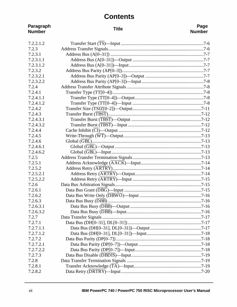
7.2.2.1.2 Transfer Start (TS)—Input .......................................................................7.2.3 Address Transfer Signals.............................................................................7.2.3.1 Address Bus (A[0–31]) ............................................................................7.2.3.1.1 Address Bus (A[0–31])—Output ..........................................................7.2.3.1.2 Address Bus (A[0–31])—Input .............................................................7.2.3.2 Address Bus Parity (AP[0–3])...................................................................7.2.3.2.1 Address Bus Parity (AP[0–3])—Output ...............................................7.2.3.2.2 Address Bus Parity (AP[0–3])—Input ...................................................7.2.4 Address Transfer Attribute Signals ..............................................................7.2.4.1 Transfer Type (TT[0–4]) ...........................................................................7.2.4.1.1 Transfer Type (TT[0–4])—Output.........................................................7.2.4.1.2 Transfer Type (TT[0–4])—Input ...........................................................7.2.4.2 Transfer Size (TSIZ[0–2])—Output..........................................................7.2.4.3 Transfer Burst (TBST)................................................................................77.2.4.3.1 Transfer Burst (TBST)—Output ............................................................7-7.2.4.3.2 Transfer Burst (TBST)—Input ...............................................................7-7.2.4.4 Cache Inhibit (CI)—Output .......................................................................77.2.4.5 Write-Through (WT)—Output...................................................................77.2.4.6 Global (GBL)..............................................................................................7.2.4.6.1 Global (GBL)—Output ..........................................................................77.2.4.6.2 Global (GBL)—Input .............................................................................77.2.5 Address Transfer Termination Signals.........................................................7.2.5.1 Address Acknowledge (AACK)—Input....................................................7-17.2.5.2 Address Retry (ARTRY)............................................................................77.2.5.2.1 Address Retry (ARTRY)—Output.........................................................7-7.2.5.2.2 Address Retry (ARTRY)—Input ...........................................................7-7.2.6 Data Bus Arbitration Signals........................................................................7.2.6.1 Data Bus Grant (DBG)—Input ..................................................................7-7.2.6.2 Data Bus Write Only (DBWO)—Input .....................................................7-17.2.6.3 Data Bus Busy (DBB) ................................................................................77.2.6.3.1 Data Bus Busy (DBB)—Output .............................................................7-7.2.6.3.2 Data Bus Busy (DBB)—Input................................................................7-7.2.7 Data Transfer Signals ..................................................................................7.2.7.1 Data Bus (DH[0–31], DL[0–31]) ...............................................................7.2.7.1.1 Data Bus (DH[0–31], DL[0–31])—Output ............................................77.2.7.1.2 Data Bus (DH[0–31], DL[0–31])—Input...............................................77.2.7.2 Data Bus Parity (DP[0–7]) .......................................................................7.2.7.2.1 Data Bus Parity (DP[0–7])—Output .....................................................7.2.7.2.2 Data Bus Parity (DP[0–7])—Input........................................................7.2.7.3 Data Bus Disable (DBDIS)—Input............................................................7-7.2.8 Data Transfer Termination Signals ..............................................................7.2.8.1 Transfer Acknowledge (TA)—Input..........................................................7-7.2.8.2 Data Retry (DRTRY)—Input.....................................................................7
xii IBM PowerPC 740 / PowerPC 750 RISC Microprocessor User’s Manual

Contents
ParagraphNumber Title Page
Number
0...7-21-211122...7-222323....7-233
424.7-2425..7-25-25
7-25-25-26
.7-267-267-26.7-267-27-27-277-27-28
7-28..7-28..7-297-297-29-30...7-30
....8-2
7.2.8.3 Transfer Error Acknowledge (TEA)—Input .............................................7-27.2.9 System Status Signals .................................................................................7.2.9.1 Interrupt (INT)—Input ..............................................................................77.2.9.2 System Management Interrupt (SMI)—Input............................................7-27.2.9.3 Machine Check Interrupt (MCP)—Input ..................................................7-27.2.9.4 Checkstop Input (CKSTP_IN)—Input......................................................7-27.2.9.5 Checkstop Output (CKSTP_OUT)—Output ............................................7-27.2.9.6 Reset Signals ...........................................................................................7.2.9.6.1 Hard Reset (HRESET)—Input ..............................................................7-7.2.9.6.2 Soft Reset (SRESET)—Input.................................................................7-7.2.9.7 Processor Status Signals.........................................................................7.2.9.7.1 Quiescent Request (QREQ)—Output....................................................7-27.2.9.7.2 Quiescent Acknowledge (QACK)—Input ............................................7-27.2.9.7.3 Reservation (RSRV)—Output ...............................................................7-7.2.9.7.4 Time Base Enable (TBEN)—Input.......................................................7.2.9.7.5 TLBI Sync (TLBISYNC)—Input ..........................................................7-7.2.9.7.6 L2 Cache Interface...............................................................................7.2.9.8 L2 Address (L2ADDR[16–0])—Output....................................................77.2.9.9 L2 Data (L2DATA[0–63]).........................................................................7.2.9.9.1 L2 Data (L2DATA[0–63])—Output......................................................77.2.9.9.2 L2 Data (L2DATA[0–63])—Input ........................................................77.2.9.10 L2 Data Parity (L2DP[0–7]) .....................................................................7.2.9.10.1 L2 Data Parity (L2DP[0–7])—Output ...................................................7.2.9.10.2 L2 Data Parity (L2DP[0–7])—Input......................................................7.2.9.11 L2 Chip Enable (L2CE)—Output .............................................................7.2.9.12 L2 Write Enable (L2WE)—Output............................................................7.2.9.13 L2 Clock Out A (L2CLK_OUTA)—Output .............................................77.2.9.14 L2 Clock Out B (L2CLK_OUTB)—Output..............................................77.2.9.15 L2 Sync Out (L2SYNC_OUT)—Output ...................................................7.2.9.16 L2 Sync In (L2SYNC_IN)—Input ............................................................77.2.9.17 L2 Low-Power Mode Enable (L2ZZ)—Output.........................................7.2.10 IEEE 1149.1a-1993 Interface Description ...................................................7.2.11 Clock Signals ...............................................................................................7.2.11.1 System Clock (SYSCLK)—Input..............................................................7.2.11.2 Clock Out (CLK_OUT)—Output ..............................................................7.2.11.3 PLL Configuration (PLL_CFG[0–3])—Input ...........................................77.2.12 Power and Ground Signals..........................................................................
Chapter 8Bus Interface Operation
8.1 Bus Interface Overview....................................................................................
Contents xiii

ContentsParagraphNumber Title Page
Number
....8-3.....8-6....8-6...8-7.....8-7....8-8..8-10..8-11...8-12..8-12...8-14...8-15..8-15.8-15.8-15.8-16.8-16..8-17.8-188-198-21..8-21...8-23..8-23-24
..8-25
...8-25
..8-26
.8-26..8-30.8-30..8-33.8-39..8-398-41...8-41...8-42..8-42...8-42...8-42...8-43....8-4343
8.1.1 Operation of the Instruction and Data L1 Caches ........................................8.1.2 Operation of the L2 Cache ..........................................................................8.1.3 Operation of the Bus Interface .....................................................................8.1.4 Optional 32-Bit Data Bus Mode....................................................................8.1.5 Direct-Store Accesses..................................................................................8.2 Memory Access Protocol..................................................................................8.2.1 Arbitration Signals........................................................................................8.2.2 Address Pipelining and Split-Bus Transactions ...........................................8.3 Address Bus Tenure.........................................................................................8.3.1 Address Bus Arbitration ...............................................................................8.3.2 Address Transfer .........................................................................................8.3.2.1 Address Bus Parity ..................................................................................8.3.2.2 Address Transfer Attribute Signals ..........................................................8.3.2.2.1 Transfer Type (TT[0–4]) Signals ..........................................................8.3.2.2.2 Transfer Size (TSIZ[0–2]) Signals ........................................................8.3.2.2.3 Write-Through (WT) Signal..................................................................8.3.2.2.4 Cache Inhibit (CI) Signal ......................................................................8.3.2.3 Burst Ordering During Data Transfers.....................................................8.3.2.4 Effect of Alignment in Data Transfers ......................................................8.3.2.4.1 Effect of Alignment in Data Transfers (32-Bit Bus)..............................8.3.2.5 Alignment of External Control Instructions...............................................8.3.3 Address Transfer Termination......................................................................8.4 Data Bus Tenure ..............................................................................................8.4.1 Data Bus Arbitration.....................................................................................8.4.1.1 Using theDBB Signal ................................................................................88.4.2 Data Bus Write Only ....................................................................................8.4.3 Data Transfer ...............................................................................................8.4.4 Data Transfer Termination ...........................................................................8.4.4.1 Normal Single-Beat Termination ..............................................................8.4.4.2 Data Transfer Termination Due to a Bus Error ........................................8.4.5 Memory Coherency—MEI Protocol .............................................................8.5 Timing Examples..............................................................................................8.6 Optional Bus Configuration ..............................................................................8.6.1 32-Bit Data Bus Mode..................................................................................8.6.2 No-DRTRY Mode..........................................................................................8.6.3 Reduced Pinout Mode .................................................................................8.7 Interrupt, Checkstop, and Reset Signals..........................................................8.7.1 External Interrupts ........................................................................................8.7.2 Checkstops...................................................................................................8.7.3 Reset Inputs .................................................................................................8.7.4 System Quiesce Control Signals .................................................................8.8 Processor State Signals...................................................................................8.8.1 Support for thelwarx/stwcx. Instruction Pair................................................8-
xiv IBM PowerPC 740 / PowerPC 750 RISC Microprocessor User’s Manual
Contents
ParagraphNumber Title Page
Number
8-44..8-44..8-44.8-45
....9-1....9-2...9-5...9-6...9-7.....9-7...9-7....9-8...9-9...9-9..9-9.9-11.9-12
..10-1...10-1...10-210-210-2..10-2..10-3...10-4...10-5..10-6.10-6.10-8.10-8.10-910-1010-1010-10
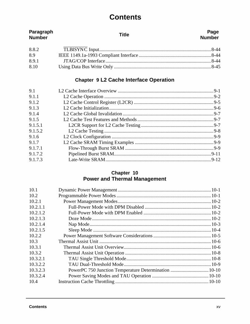
8.8.2 TLBISYNC Input...........................................................................................8.9 IEEE 1149.1a-1993 Compliant Interface.........................................................8.9.1 JTAG/COP Interface....................................................................................8.10 Using Data Bus Write Only ..............................................................................
Chapter 9 L2 Cache Interface Operation
9.1 L2 Cache Interface Overview ..........................................................................9.1.1 L2 Cache Operation .....................................................................................9.1.2 L2 Cache Control Register (L2CR) ..............................................................9.1.3 L2 Cache Initialization..................................................................................9.1.4 L2 Cache Global Invalidation .......................................................................9.1.5 L2 Cache Test Features and Methods .........................................................9.1.5.1 L2CR Support for L2 Cache Testing ........................................................9.1.5.2 L2 Cache Testing .....................................................................................9.1.6 L2 Clock Configuration ................................................................................9.1.7 L2 Cache SRAM Timing Examples .............................................................9.1.7.1 Flow-Through Burst SRAM ......................................................................9.1.7.2 Pipelined Burst SRAM..............................................................................9.1.7.3 Late-Write SRAM.....................................................................................
Chapter 10Power and Thermal Management
10.1 Dynamic Power Management ..........................................................................10.2 Programmable Power Modes ..........................................................................10.2.1 Power Management Modes.........................................................................10.2.1.1 Full-Power Mode with DPM Disabled ......................................................10.2.1.2 Full-Power Mode with DPM Enabled .......................................................10.2.1.3 Doze Mode...............................................................................................10.2.1.4 Nap Mode.................................................................................................10.2.1.5 Sleep Mode .............................................................................................10.2.2 Power Management Software Considerations ............................................10.3 Thermal Assist Unit .........................................................................................10.3.1 Thermal Assist Unit Overview......................................................................10.3.2 Thermal Assist Unit Operation .....................................................................10.3.2.1 TAU Single Threshold Mode....................................................................10.3.2.2 TAU Dual-Threshold Mode......................................................................10.3.2.3 PowerPC 750 Junction Temperature Determination ...............................10.3.2.4 Power Saving Modes and TAU Operation ..............................................10.4 Instruction Cache Throttling ............................................................................
Contents xv

ContentsParagraphNumber Title Page
Number
..11-2...11-3...11-311-31-5
11-51-6
.11-61-1011-1011-11.11-11.11-12.11-12
...A-1...A-9.A-17.A-29.A-41
...B-1
...G-1
Chapter 11Performance Monitor
11.1 Performance Monitor Interrupt.........................................................................11.2 Special-Purpose Registers Used by Performance Monitor..............................11.2.1 Performance Monitor Registers...................................................................11.2.1.1 Monitor Mode Control Register 0 (MMCR0)............................................11.2.1.2 User Monitor Mode Control Register 0 (UMMCR0) ................................111.2.1.3 Monitor Mode Control Register 1 (MMCR1)............................................11.2.1.4 User Monitor Mode Control Register 1 (UMMCR1) ................................111.2.1.5 Performance Monitor Counter Registers (PMC1–PMC4) ........................11.2.1.6 User Performance Monitor Counter Registers (UPMC1–UPMC4).........111.2.1.7 Sampled Instruction Address Register (SIA) ...........................................11.2.1.8 User Sampled Instruction Address Register (USIA)................................11.3 Event Counting................................................................................................11.4 Event Selection................................................................................................11.5 Notes................................................................................................................
Appendix APowerPC Instruction Set Listings
A.1 Instructions Sorted by Mnemonic.....................................................................A.2 Instructions Sorted by Opcode .........................................................................A.3 Instructions Grouped by Functional Categories ...............................................A.4 Instructions Sorted by Form .............................................................................A.5 Instruction Set Legend......................................................................................
Appendix BInstructions Not Implemented
B.1 Lists of Instructions ..........................................................................................
Glossary of Terms and Abbreviations
G.1 Alphabetical List...............................................................................................
Index
xvi IBM PowerPC 740 / PowerPC 750 RISC Microprocessor User’s Manual

Illustrations
ParagraphNumber Title Page
Number
....1-3...1-13....1-16...1-18..1-23...1-34....2-2....2-9....2-9..2-132-142-16..2-16..2-202-21.2-22..2-23..2-24.....3-2.....3-4.....3-5...3-8..3-193-23......4-7......4-7.....4-8..4-14.5-6..5-7..5-8...5-10.5-13..5-15..5-26.5-29....5-32....5-33....6-4.....6-5......6-7..6-10.6-12
Figure 1-1 PowerPC 750 Microprocessor Block Diagram ................................................Figure 1-2 Cache Organization.........................................................................................Figure 1-3 System Interface.............................................................................................Figure 1-4 PowerPC 750 Microprocessor Signal Groups.................................................Figure 1-5 PowerPC 750 Microprocessor Programming Model—Registers ....................Figure 1-6 Pipeline Diagram.............................................................................................Figure 2-1 Programming Model—PowerPC 750 Microprocessor Registers ....................Figure 2-2 Instruction Address Breakpoint Register .........................................................Figure 2-3 Hardware Implementation-Dependent Register 0 (HID0) ...............................Figure 2-4 Hardware Implementation-Dependent Register 1 (HID1) ...............................Figure 2-5 Monitor Mode Control Register 0 (MMCR0)....................................................Figure 2-6 Monitor Mode Control Register 1 (MMCR1)....................................................Figure 2-7 Performance Monitor Counter Registers (PMC1–PMC4)...............................Figure 2-8 Sampled Instruction Address Registers (SIA) .................................................Figure 2-9 Instruction Cache Throttling Control Register (ICTC)......................................Figure 2-10 Thermal Management Registers 1–2 (THRM1–THRM2)................................Figure 2-11 Thermal Management Register 3 (THRM3)....................................................Figure 2-12 L2 Cache Control Register (L2CR) .................................................................Figure 3-1 Cache Integration ............................................................................................Figure 3-2 Data Cache Organization ................................................................................Figure 3-3 Instruction Cache Organization.......................................................................Figure 3-4 MEI Cache Coherency Protocol—State Diagram (WIM = 001) ......................Figure 3-5 PLRU Replacement Algorithm ........................................................................Figure 3-6 Double-Word Address Ordering—Critical Double Word First.........................Figure 4-1 Machine Status Save/Restore Register 0 (SRR0) ..........................................Figure 4-2 Machine Status Save/Restore Register 1 (SRR1) ..........................................Figure 4-3 Machine State Register (MSR) .......................................................................Figure 4-4 SRESET Asserted During HRESET................................................................Figure 5-1 MMU Conceptual Block Diagram—32-Bit Implementations............................Figure 5-2 PowerPC 750 Microprocessor IMMU Block Diagram......................................Figure 5-3 PowerPC 750 Microprocessor DMMU Block Diagram ....................................Figure 5-4 Address Translation Types..............................................................................Figure 5-5 General Flow of Address Translation (Real Addressing Mode and Block) .....Figure 5-6 General Flow of Page and Direct-Store Interface Address Translation...........Figure 5-7 Segment Register and DTLB Organization .....................................................Figure 5-8 Page Address Translation Flow—TLB Hit.......................................................Figure 5-9 Primary Page Table Search ............................................................................Figure 5-10 Secondary Page Table Search Flow...............................................................Figure 6-1 Pipelined Execution Unit .................................................................................Figure 6-2 Superscalar/Pipeline Diagram.........................................................................Figure 6-3 PowerPC 750 Microprocessor Pipeline Stages ..............................................Figure 6-4 Instruction Flow Diagram ................................................................................Figure 6-5 Instruction Timing—Cache Hit.........................................................................
Illustrations xvii

IllustrationsParagraphNumber Title Page
Number
..6-15...6-19.6-19...6-20..6-23......7-3.....8-2....8-5....8-8.....8-9...8-12..8-13....8-1523...8-24...8-27..8-27...8-28.8-29-29.8-32.....8-33....8-34...8-35..8-36..8-378..8-40
...8-44
...8-45...9-2..9-10.9-10.9-11...9-11.9-12..9-12..9-139-13.9-14..10-6.11-4.11-5
Figure 6-6 Instruction Timing—Cache Miss .....................................................................Figure 6-7 Branch Folding ................................................................................................Figure 6-8 Removal of Fall-Through Branch Instruction ...................................................Figure 6-9 Branch Completion..........................................................................................Figure 6-10 Branch Instruction Timing................................................................................Figure 7-1 PowerPC 750 Signal Groups ..........................................................................Figure 8-1 Bus Interface Address Buffers.........................................................................Figure 8-2 PowerPC 750 Microprocessor Block Diagram ................................................Figure 8-3 Timing Diagram Legend ..................................................................................Figure 8-4 Overlapping Tenures on the 750 Bus for a Single-Beat Transfer ...................Figure 8-5 Address Bus Arbitration ..................................................................................Figure 8-6 Address Bus Arbitration Showing Bus Parking ...............................................Figure 8-7 Address Bus Transfer .....................................................................................Figure 8-8 Snooped Address Cycle withARTRY................................................................8-Figure 8-9 Data Bus Arbitration........................................................................................Figure 8-10 Normal Single-Beat Read Termination ...........................................................Figure 8-11 Normal Single-Beat Write Termination ...........................................................Figure 8-12 Normal Burst Transaction ...............................................................................Figure 8-13 Termination with DRTRY .................................................................................Figure 8-14 Read Burst withTA Wait States and DRTRY....................................................8Figure 8-15 MEI Cache Coherency Protocol—State Diagram (WIM = 001) ......................Figure 8-16 Fastest Single-Beat Reads .............................................................................Figure 8-17 Fastest Single-Beat Writes..............................................................................Figure 8-18 Single-Beat Reads Showing Data-Delay Controls ..........................................Figure 8-19 Single-Beat Writes Showing Data Delay Controls...........................................Figure 8-20 Burst Transfers with Data Delay Controls .......................................................Figure 8-21 Use of Transfer Error Acknowledge (TEA) .......................................................8-3Figure 8-22 32-Bit Data Bus Transfer (Eight-Beat Burst) ...................................................Figure 8-23 32-Bit Data Bus Transfer (Two-Beat Burst withDRTRY) ................................8-40Figure 8-24 IEEE 1149.1a-1993 Compliant Boundary Scan Interface...............................Figure 8-25 Data Bus Write Only Transaction ...................................................................Figure 9-26 Typical 1-Mbyte L2 Cache Configuration ........................................................Figure 9-27 Burst Read-Write-Read L2 Cache Access (Flow-Through).............................Figure 9-28 Burst Read-Modify-Write L2 Cache Access (Flow-Through)..........................Figure 9-29 Burst Read-Write-Write L2 Cache Access (Flow-Through).............................Figure 9-30 Burst Read-Write-Read L2 Cache Access (Pipelined)....................................Figure 9-31 Burst Read-Modify-Write L2 Cache Access (Pipelined) ..................................Figure 9-32 Burst Read-Write-Write L2 Cache Access (Pipelined)....................................Figure 9-33 Burst Read-Write-Read L2 Cache Access (Late-Write SRAM)......................Figure 9-34 Burst Read-Modify-Write L2 Cache Access (Late-Write SRAM) ....................Figure 9-35 Burst Read-Write-Write L2 Cache Access (Late-Write SRAM) ......................Figure 10-1 Thermal Assist Unit Block Diagram ................................................................Figure 11-1 Monitor Mode Control Register 0 (MMCR0) ...................................................Figure 11-2 Monitor Mode Control Register 1 (MMCR1) ...................................................
xviii IBM PowerPC 740 / PowerPC 750 RISC Microprocessor User’s Manual

Illustrations
ParagraphNumber Title Page
Number
..11-6
.11-10
Figure 11-3 Performance Monitor Counter Registers (PMC1–PMC4)...............................Figure 11-4 Sampled instruction Address Registers (SIA).................................................Illustrations xix

IllustrationsParagraphNumber Title Page
Number
xx IBM PowerPC 740 / PowerPC 750 RISC Microprocessor User’s Manual

Tables
ParagraphNumber Title Page
Number
... xxxxxxivxxxv..1-24..1-25..1-26..1-31...1-31...2-4....2-6....2-9....2-93
..2-13
..2-14
..2-16
...2-17.2-17.2-18.2-18.2-19..2-21.2-22.2-23..2-24..2-25..2-30..2-31..2-38...2-39..2-40...2-41..2-41.2-422-43..2-43..2-43..2-44..2-44...2-47...2-48..2-49..2-49
Table i Acronyms and Abbreviated Terms .................................................................Table ii Terminology Conventions ...............................................................................Table iii Instruction Field Conventions ..........................................................................Table 1-1 Architecture-Defined Registers (Excluding SPRs) ..........................................Table 1-2 Architecture-Defined SPRs Implemented........................................................Table 1-3 Implementation-Specific Registers ..................................................................Table 1-4 PowerPC 750 Microprocessor Exception Classifications ...............................Table 1-5 Exceptions and Conditions .............................................................................Table 2-1 Additional MSR Bits.........................................................................................Table 2-2 Additional SRR1 Bits.......................................................................................Table 2-3 Instruction Address Breakpoint Register Bit Settings......................................Table 2-4 HID0 Bit Functions .........................................................................................Table 2-5 HID0[BCLK] and HID0[ECLK] CLK_OUT Configuration.............................2-1Table 2-6 HID1 Bit Functions ..........................................................................................Table 2-7 MMCR0 Bit Settings .......................................................................................Table 2-8 MMCR1 Bit Settings........................................................................................Table 2-9 PMCn Bit Settings...........................................................................................Table 2-10 PMC1 Events—MMCR0[19–25] Select Encodings.........................................Table 2-11 PMC2 Events—MMCR0[26–31] Select Encodings.........................................Table 2-12 PMC3 Events—MMCR1[0–4] Select Encodings ............................................Table 2-13 PMC4 Events—MMCR1[5–9] Select Encodings.............................................Table 2-14 ICTC Bit Settings.............................................................................................Table 2-15 THRM1–THRM2 Bit Settings..........................................................................Table 2-16 Valid THRM1/THRM2 States ..........................................................................Table 2-17 THRM3 Bit Settings ........................................................................................Table 2-18 L2CR Bit Settings ...........................................................................................Table 2-19 Floating-Point Operand Data Type Behavior ..................................................Table 2-20 Floating-Point Result Data Type Behavior .....................................................Table 2-21 Integer Arithmetic Instructions .......................................................................Table 2-22 Integer Compare Instructions..........................................................................Table 2-23 Integer Logical Instructions ............................................................................Table 2-24 Integer Rotate Instructions .............................................................................Table 2-25 Integer Shift Instructions .................................................................................Table 2-26 Floating-Point Arithmetic Instructions ............................................................Table 2-27 Floating-Point Multiply-Add Instructions .........................................................Table 2-28 Floating-Point Rounding and Conversion Instructions ...................................Table 2-29 Floating-Point Compare Instructions ...............................................................Table 2-30 Floating-Point Status and Control Register Instructions .................................Table 2-31 Floating-Point Move Instructions ...................................................................Table 2-32 Integer Load Instructions ...............................................................................Table 2-33 Integer Store Instructions ...............................................................................Table 2-34 Integer Load and Store with Byte-Reverse Instructions .................................Table 2-35 Integer Load and Store Multiple Instructions .................................................
Tables xxi

TablesParagraphNumber Title Page
Number
...2-50
..2-51...2-52...2-52..2-53...2-54..2-54...2-55..2-55..2-56..2-56....2-56
.2-59..2-60.2-62...2-63...2-64..2-65..2-65..2-66...2-66...2-67..2-67....3-7...3-20...3-20..3-24.....3-27..3-29...3-31....4-2.....4-3.....4-6.....4-8.4-10...4-12....4-13....4-15.....4-16..4-17...4-18...4-22
Table 2-36 Integer Load and Store String Instructions .....................................................Table 2-37 Floating-Point Load Instructions .....................................................................Table 2-38 Floating-Point Store Instructions ....................................................................Table 2-39 Store Floating-Point Single Behavior .............................................................Table 2-40 Store Floating-Point Double Behavior ............................................................Table 2-41 Branch Instructions..........................................................................................Table 2-42 Condition Register Logical Instructions ..........................................................Table 2-43 Trap Instructions..............................................................................................Table 2-44 System Linkage Instruction—UISA.................................................................Table 2-45 Move to/from Condition Register Instructions.................................................Table 2-46 Move to/from Special-Purpose Register Instructions (UISA)..........................Table 2-47 PowerPC Encodings ......................................................................................Table 2-48 SPR Encodings for PowerPC 750-Defined Registers (mfspr) .........................2-58Table 2-49 Memory Synchronization Instructions—UISA ...............................................Table 2-50 Move from Time Base Instruction....................................................................Table 2-51 Memory Synchronization Instructions—VEA ..................................................Table 2-52 User-Level Cache Instructions ......................................................................Table 2-53 External Control Instructions...........................................................................Table 2-54 System Linkage Instructions—OEA ................................................................Table 2-55 Move to/from Machine State Register Instructions..........................................Table 2-56 Move to/from Special-Purpose Register Instructions (OEA)...........................Table 2-57 Supervisor-Level Cache Management Instruction ..........................................Table 2-58 Segment Register Manipulation Instructions ..................................................Table 2-59 Translation Lookaside Buffer Management Instruction...................................Table 3-1 MEI State Definitions.......................................................................................Table 3-2 PLRU Bit Update Rules ..................................................................................Table 3-3 PLRU Replacement Block Selection...............................................................Table 3-4 Bus Operations Caused by Cache Control Instructions (WIM = 001).............Table 3-5 Response to Snooped Bus Transactions .......................................................Table 3-6 Address/Transfer Attribute Summary ............................................................Table 3-7 MEI State Transitions .....................................................................................Table 4-1 PowerPC 750 Microprocessor Exception Classifications ...............................Table 4-2 Exceptions and Conditions .............................................................................Table 4-3 PowerPC 750 Exception Priorities .................................................................Table 4-4 MSR Bit Settings ............................................................................................Table 4-5 IEEE Floating-Point Exception Mode Bits ......................................................Table 4-6 MSR Setting Due to Exception ......................................................................Table 4-7 System Reset Exception—Register Settings .................................................Table 4-8 HRESET Signal States ...................................................................................Table 4-9 Settings Caused by Hard Reset .....................................................................Table 4-10 HID0 Machine Check Enable Bits ...................................................................Table 4-11 Machine Check Exception—Register Settings................................................Table 4-12 Trace Exception—SRR1 Settings ...................................................................
xxii IBM PowerPC 740 / PowerPC 750 RISC Microprocessor User’s Manual
Tables
ParagraphNumber Title Page
Number
.4-23..4-24...4-25..4-26....5-3....5-11..5-17.5-185-19..5-20.5-22..5-24...6-26..6-28...6-31...6-31.6-32...6-33..6-34...6-36....7-9....7-10...7-11...7-17..7-18..7-28...8-16...8-17.8-17...8-18..8-19.8-20.8-21.....9-5...10-2.10-7..10-710-910-11...11-3..11-4..11-6...11-6
Table 4-13 Performance Monitor Interrupt Exception—Register Settings ........................Table 4-14 Instruction Address Breakpoint Exception—Register Settings ......................Table 4-15 System Management Interrupt Exception—Register Settings .......................Table 4-16 Thermal Management Interrupt Exception—Register Settings ......................Table 5-1 MMU Feature Summary .................................................................................Table 5-2 Access Protection Options for Pages ............................................................Table 5-3 Translation Exception Conditions ...................................................................Table 5-4 Other MMU Exception Conditions for the PowerPC 750 Processor................Table 5-5 PowerPC 750 Microprocessor Instruction Summary—Control MMUs............Table 5-6 PowerPC 750 Microprocessor MMU Registers ..............................................Table 5-7 Table Search Operations to Update History Bits—TLB Hit Case....................Table 5-8 Model for Guaranteed R and C Bit Settings ..................................................Table 6-1 Performance Effects of Memory Operand Placement.....................................Table 6-2 TLB Miss Latencies ........................................................................................Table 6-3 Branch Instructions .........................................................................................Table 6-4 System Register Instructions ..........................................................................Table 6-5 Condition Register Logical Instructions ..........................................................Table 6-6 Integer Instructions .........................................................................................Table 6-7 Floating-Point Instructions ..............................................................................Table 6-8 Load and Store Instructions ............................................................................Table 7-1 Transfer Type Encodings for PowerPC 750 Bus Master ................................Table 7-2 PowerPC 750 Snoop Hit Response ...............................................................Table 7-3 Data Transfer Size ..........................................................................................Table 7-4 Data Bus Lane Assignments ..........................................................................Table 7-5 DP[0–7] Signal Assignments ..........................................................................Table 7-6 IEEE Interface Pin Descriptions ......................................................................Table 8-1 Transfer Size Signal Encodings .....................................................................Table 8-2 Burst Ordering.................................................................................................Table 8-3 Burst Ordering—32-Bit Bus ............................................................................Table 8-4 Aligned Data Transfers ..................................................................................Table 8-5 Misaligned Data Transfers (Four-Byte Examples) .........................................Table 8-6 Aligned Data Transfers (32-Bit Bus Mode)......................................................Table 8-7 Misaligned 32-Bit Data Bus Transfer (Four-Byte Examples) .........................Table 9-8 L2 Cache Control Register .............................................................................Table 10-1 PowerPC 750 Microprocessor Programmable Power Modes.........................Table 10-2 THRM1 and THRM2 Bit Field Settings...........................................................Table 10-3 THRM3 Bit Field Settings ...............................................................................Table 10-4 Valid THRM1 and THRM2 Bit Settings ..........................................................Table 10-5 ICTC Bit Field Settings....................................................................................Table 11-1 Performance Monitor SPRs.............................................................................Table 11-2 MMCR0 Bit Settings .......................................................................................Table 11-3 MMCR1 Bit Settings........................................................................................Table 11-4 PMCn Bit Settings...........................................................................................
Tables xxiii
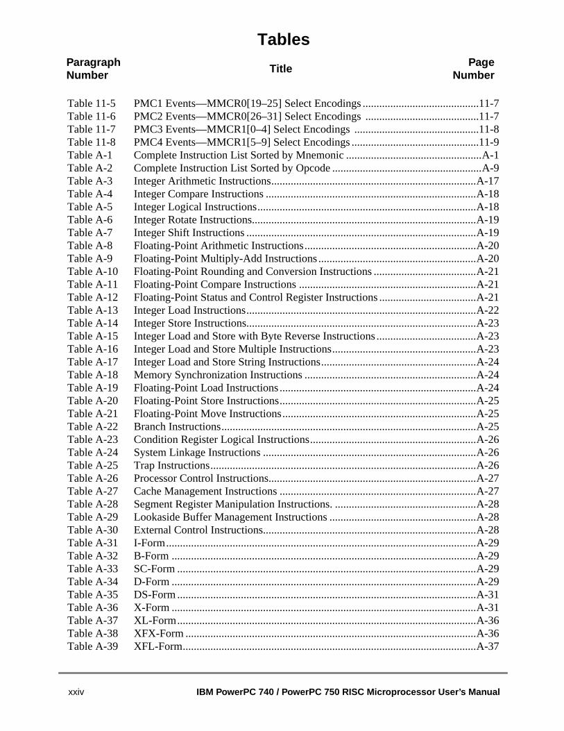
TablesParagraphNumber Title Page
Number
..11-7.11-7.11-8..11-9..A-1...A-9.A-17..A-18.A-18..A-19.A-19A-20-20
.A-21.A-21.A-21..A-22..A-23..A-23.A-23..A-24.A-24.A-24.A-25.A-25..A-25.A-26..A-26..A-26..A-27...A-27.A-28.A-28.A-28....A-..A-2..A-..A-3..A-.A-3.A-36.A-37
Table 11-5 PMC1 Events—MMCR0[19–25] Select Encodings ........................................Table 11-6 PMC2 Events—MMCR0[26–31] Select Encodings ........................................Table 11-7 PMC3 Events—MMCR1[0–4] Select Encodings ............................................Table 11-8 PMC4 Events—MMCR1[5–9] Select Encodings ............................................Table A-1 Complete Instruction List Sorted by Mnemonic ...............................................Table A-2 Complete Instruction List Sorted by Opcode ...................................................Table A-3 Integer Arithmetic Instructions.........................................................................Table A-4 Integer Compare Instructions ..........................................................................Table A-5 Integer Logical Instructions..............................................................................Table A-6 Integer Rotate Instructions...............................................................................Table A-7 Integer Shift Instructions ..................................................................................Table A-8 Floating-Point Arithmetic Instructions..............................................................Table A-9 Floating-Point Multiply-Add Instructions.........................................................ATable A-10 Floating-Point Rounding and Conversion Instructions ....................................Table A-11 Floating-Point Compare Instructions ...............................................................Table A-12 Floating-Point Status and Control Register Instructions ..................................Table A-13 Integer Load Instructions.................................................................................Table A-14 Integer Store Instructions.................................................................................Table A-15 Integer Load and Store with Byte Reverse Instructions..................................Table A-16 Integer Load and Store Multiple Instructions...................................................Table A-17 Integer Load and Store String Instructions......................................................Table A-18 Memory Synchronization Instructions .............................................................Table A-19 Floating-Point Load Instructions......................................................................Table A-20 Floating-Point Store Instructions......................................................................Table A-21 Floating-Point Move Instructions.....................................................................Table A-22 Branch Instructions..........................................................................................Table A-23 Condition Register Logical Instructions...........................................................Table A-24 System Linkage Instructions ...........................................................................Table A-25 Trap Instructions..............................................................................................Table A-26 Processor Control Instructions.........................................................................Table A-27 Cache Management Instructions ....................................................................Table A-28 Segment Register Manipulation Instructions. ..................................................Table A-29 Lookaside Buffer Management Instructions ....................................................Table A-30 External Control Instructions............................................................................Table A-31 I-Form..............................................................................................................A-29Table A-32 B-Form ............................................................................................................29Table A-33 SC-Form ..........................................................................................................9Table A-34 D-Form ............................................................................................................29Table A-35 DS-Form ..........................................................................................................1Table A-36 X-Form ............................................................................................................31Table A-37 XL-Form...........................................................................................................6Table A-38 XFX-Form ........................................................................................................Table A-39 XFL-Form.........................................................................................................
xxiv IBM PowerPC 740 / PowerPC 750 RISC Microprocessor User’s Manual

Tables
ParagraphNumber Title Page
Number
..A-3.A-37.A-.A-3.A-39.A-40..A-41..A-47.. B-1.. B-1
Table A-40 XS-Form..........................................................................................................7Table A-41 XO-Form ..........................................................................................................Table A-42 A-Form.............................................................................................................38Table A-43 M-Form ............................................................................................................9Table A-44 MD-Form .........................................................................................................Table A-45 MDS-Form .......................................................................................................Table A-46 PowerPC Instruction Set Legend ..................................................................Table A-47 PowerPC Instruction Set Legend ..................................................................Table B-1 32-Bit Instructions Not Implemented................................................................Table B-2 64-Bit Instructions Not Implemented ...............................................................
Tables xxv

TablesParagraphNumber Title Page
Number
xxvi IBM PowerPC 740 / PowerPC 750 RISC Microprocessor User’s Manual
rPClopers.d, all
thiss:
hat a
ows:
l ofthetions,
About This BookThe primary objective of this user’s manual is to define the functionality of the Powe750™ and PowerPC 740™ microprocessors for use by software and hardware deveAlthough the emphasis of this manual is upon the 750, unless otherwise noteinformation here applies to 740. This book is intended as a companion to thePowerPC™Microprocessor Family: The Programming Environments(referred to asThe ProgrammingEnvironments Manual).
Note: Soft copies of the latest version of this manual and documents referred to inmanual that are produced by IBM can be accessed on the world wide web as follow
http://www.chips.ibm.com/
Note: A vertical bar located to the left of a paragraph such as this one, indicates tchange has been made to the paragraph since the 8/97 release of this document.
About the Companion Programming Environments Manual
ThePowerPC 740 PowerPC750 RISC Microprocessor User’sManual, which describes 750 features not defined by thearchitecture, is to be used with thePowerPC MicroprocessorFamily: The Programming Environments, Rev. 1, referred to asThe Programming Environments Manual.
Because the PowerPC architecture is designed to be flexible tosupport a broad range of processors,The ProgrammingEnvironments Manualprovides a general description offeatures that are common to PowerPC processors and indicatesthose features that are optional or that may be implementeddifferently in the design of each processor.
Contact your sales representative for a copy ofTheProgramming Environments Manual.
This document andThe Programming Environments Manualdistinguish between the threelevels, or programming environments, of the PowerPC architecture, which are as foll
• PowerPC user instruction set architecture (UISA)—The UISA defines the levethe architecture to which user-level software should conform. The UISA definesbase user-level instruction set, user-level registers, data types, memory convenand the memory and programming models seen by application programmers.
About This Book xxvii

estality theeshe
VEArcesternal
rPC
isor-eption
rPC
in theating-fined
er toarly
aand
cache,ationodel
mainsring
thethe
f the
• PowerPC virtual environment architecture (VEA)—The VEA, which is the smallcomponent of the PowerPC architecture, defines additional user-level functionthat falls outside typical user-level software requirements. The VEA describesmemory model for an environment in which multiple processors or other deviccan access external memory and defines aspects of the cache model and caccontrol instructions from a user-level perspective. The resources defined by theare particularly useful for optimizing memory accesses and for managing resouin an environment in which other processors and other devices can access exmemory.
Implementations that conform to the PowerPC VEA also conform to the PoweUISA, but may not necessarily adhere to the OEA.
• PowerPC operating environment architecture (OEA)—The OEA defines supervlevel resources typically required by an operating system. The OEA defines thPowerPC memory management model, supervisor-level registers, and the excemodel.
Implementations that conform to the PowerPC OEA also conform to the PoweUISA and VEA.
It is important to note that some resources are defined more generally at one levelarchitecture and more specifically at another. For example, conditions that cause a flopoint exception are defined by the UISA, while the exception mechanism itself is deby the OEA.
Because it is important to distinguish between the levels of the architecture in ordensure compatibility across multiple platforms, those distinctions are shown clethroughout this book.
For ease in reference, the arrangement of topics in this book follows that ofTheProgramming Environments Manual. Topics build upon one another, beginning withdescription and complete summary of 750-specific registers and instructionsprogressing to more specialized topics such as 750-specific details regarding theexception, and memory management models. As such, chapters may include informfrom multiple levels of the architecture. (For example, the discussion of the cache muses information from both the VEA and the OEA.)
The PowerPC Architecture: A Specification for a New Family of RISC Processorsdefinesthe architecture from the perspective of the three programming environments and rethe defining document for the PowerPC architecture. For information about ordePowerPC documentation, see “Suggested Reading,” on page xxviii.
The information in this book is subject to change without notice, as described indisclaimers on the title page of this book. As with any technical documentation, it isreaders’ responsibility to be sure they are using the most recent version odocumentation.
xxviii IBM PowerPC 740 / PowerPC 750 RISC Microprocessor User’s Manual

ted at
ationseaderf RISC
antcturecture theodel,
odingnized
C
s,ient..
the
se ofn the
wer
To locate any published errata or updates for this document, refer to the web sites nothe beginning of this section.
AudienceThis manual is intended for system software and hardware developers and applicprogrammers who want to develop products for the 750. It is assumed that the runderstands operating systems, microprocessor system design, basic principles oprocessing, and details of the PowerPC architecture.
OrganizationFollowing is a summary and a brief description of the major sections of this manual:
• Chapter 1, “PowerPC 740/PowerPC 750 Overview,” is useful for readers who wa general understanding of the features and functions of the PowerPC architeand the 750. This chapter describes the flexible nature of the PowerPC architedefinition, and provides an overview of how the PowerPC architecture definesregister set, operand conventions, addressing modes, instruction set, cache mexception model, and memory management model.
• Chapter 2, “Programming Model,” is useful for software engineers who need tunderstand the 750-specific registers, operand conventions, and details regarhow PowerPC instructions are implemented on the 750. Instructions are orgaby function.
• Chapter 3, “Instruction and Data Cache Operation,” discusses the cache andmemory model as implemented on the 750.
• Chapter 4, “Exceptions,” describes the exception model defined in the PowerPOEA and the specific exception model implemented on the 750.
• Chapter 5, “Memory Management,” describes the 750’s implementation of thememory management unit specifications provided by the PowerPC OEA forPowerPC processors.
• Chapter 6, “Instruction Timing,” provides information about latencies, interlockspecial situations, and various conditions to help make programming more efficThis chapter is of special interest to software engineers and system designers
• Chapter 7, “Signal Descriptions,” provides descriptions of individual signals of750.
• Chapter 8, “Bus Interface Operation,” describes signal timings for variousoperations. It also provides information for interfacing to the 750.
• Chapter 9, “L2 Cache Interface Operation,” describes the implementation and uthe 750 L2 cache and cache controller. Note that this feature is not supported o740.
• Chapter 10, “Power and Thermal Management,” provides information about posaving and thermal management modes for the 750.
About This Book xxix
ce
nslsoed
vel,.
64-
this
cture
0.A.),
web
04;
pted
ver ofdering:
• Chapter 11, “Performance Monitor,” describes the operation of the performanmonitor diagnostic tool incorporated in the 750.
• Appendix A, “PowerPC Instruction Set Listings,” lists all the PowerPC instructiowhile indicating those instructions which are not implemented by the 750; it aincludes the instructions which are specific to the 750. Instructions are groupaccording to mnemonic, opcode, function, and form. Also included is a quickreference table that contains general information, such as the architecture leprivilege level, and form, and indicates if the instruction is 64-bit and optional
• Appendix B, “Instructions Not Implemented,” provides a list of the 32-bit and bit PowerPC instructions that are not implemented in the 750.
• This manual also includes a glossary and an index.
Suggested ReadingThis section lists additional reading that provides background for the information inmanual as well as general information about the PowerPC architecture.
General InformationThe following documentation provides useful information about the PowerPC architeand computer architecture in general:
• The following books are available from the Morgan-Kaufmann Publishers, 34Pine Street, Sixth Floor, San Francisco, CA 94104; Tel. (800) 745-7323 (U.S(415) 392-2665 (International); internet address: [email protected].
— The PowerPC Architecture: A Specification for a New Family of RISCProcessors, Second Edition, by International Business Machines, Inc.
Updates to the architecture specification are accessible via the world-wideat http://www.austin.ibm.com/tech/ppc-chg.html.
• PowerPC Programming for Intel Programmers,by Kip McClanahan; IDG BooksWorldwide, Inc., 919 East Hillsdale Boulevard, Suite 400, Foster City, CA, 944Tel. (800) 434-3422 (U.S.A.), (415) 655-3022 (International).
• PowerPC System Architecture,by Tom Shanley; Mindshare, Inc., 2202 ButtercuDrive, Richardson, TX 75082; Tel. (214)231-2216 (U.S.A.), 021-706 6000 (UniKingdom), (800)420-2677 (International).
PowerPC DocumentationThe PowerPC documentation is available from the sources listed inside the front cothis manual; the document order numbers are included in parentheses for ease in or
• Programming environments manuals—This book provides information aboutresources defined by the PowerPC architecture that are common to PowerPCprocessors.
xxx IBM PowerPC 740 / PowerPC 750 RISC Microprocessor User’s Manual

ts
dingashe
arynt to
sace,This
mily
, and
erPC
al
— PowerPC Microprocessor Family: The Programming EnvironmentsG522-0290-00
• Implementation Variances Relative to Rev. 1 of The Programming EnvironmenManual is available via the world-wide web at http://www.chips.ibm.com/.
• Hardware specifications—Hardware specifications provide specific data regarbus timing, signal behavior, and AC, DC, and thermal characteristics, as well other design considerations for each PowerPC implementation. This include tfollowing:
— PowerPC 740TM and PowerPC 750TM Embedded RISC Microprocessor:Hardware Specificationsis available via the world-wide web athttp://www.chips.ibm.com/.
— PowerPC 750TM SCM RISC Microprocessor: Hardware SpecificationG522-0324-00
• Technical Summaries—Each PowerPC implementation has a technical summthat provides an overview of its features. This document is roughly the equivalethe overview (Chapter 1) of an implementation’s user’s manual.
— PowerPC 750 RISC Microprocessor Technical Summaryis available via theworld-wide web at http://www.chips.ibm.com/.
• PowerPC Microprocessor Family: 60x Bus Interface for 32-Bit Microprocessor,G522-0291-00, provides a detailed functional description of the 60x bus interfas implemented on the 601, 603, and 604 family of PowerPC microprocessors.document is intended to help system and chipset developers by providing acentralized reference source to identify the bus interface presented by the 60x faof PowerPC microprocessors.
• PowerPC Microprocessor Family: The Programmer’s Reference Guide,MPRPPCPRG-01, is a concise reference that includes the register summary,memory control model, exception vectors, and the PowerPC instruction set.
• PowerPC Microprocessor Family: The Programmer’s Pocket Reference Guide,SA14-2093-00This foldout card provides an overview of the PowerPC registers, instructionsexceptions for 32-bit implementations.
• Application notes—These short documents contain useful information aboutspecific design issues useful to programmers and engineers working with Powprocessors.
• Documentation for support chips—These include the following:
— IBM27-82660 PowerPC to PCI Bridge and Memory Controller User’s ManuSC09-3026-01
About This Book xxxi

ssorslisted
ext.
ine
on’t
itsas
Additional literature on PowerPC implementations is being released as new procebecome available. For a current list of PowerPC documentation, refer to the web sitesat the beginning of this section.
ConventionsThis document uses the following notational conventions:
mnemonics Instruction mnemonics are shown in lowercase bold.
italics Italics indicate variable command parameters, for example, bcctrx.Book titles in text are set in italics.
0x0 Prefix to denote hexadecimal number
0b0 Prefix to denote binary number
rA, rB Instruction syntax used to identify a source GPR
rD Instruction syntax used to identify a destination GPR
fr A, fr B, fr C Instruction syntax used to identify a source FPR
fr D Instruction syntax used to identify a destination FPR
REG[FIELD] Abbreviations or acronyms for registers are shown in uppercase tSpecific bits, fields, or ranges appear in brackets. For example,MSR[LE] refers to the little-endian mode enable bit in the machstate register.
x In certain contexts, such as a signal encoding, this indicates a dcare.
n Used to express an undefined numerical value
¬ NOT logical operator
& AND logical operator
| OR logical operator
Indicates reserved bits or bit fields in a register. Although these bmay be written to as either ones or zeros, they are always read zeros.
Acronyms and AbbreviationsTable i contains acronyms and abbreviations that are used in this document.
Table i. Acronyms and Abbreviated Terms
Term Meaning
BAT Block address translation
BIST Built-in self test
BHT Branch history table
0 0 0 0
xxxii IBM PowerPC 740 / PowerPC 750 RISC Microprocessor User’s Manual

BIU Bus interface unit
BPU Branch processing unit
BTIC Branch target instruction cache
BSDL Boundary-scan description language
BUID Bus unit ID
CMOS Complementary metal-oxide semiconductor
COP Common on-chip processor
CR Condition register
CQ Completion queue
CTR Count register
DABR Data address breakpoint register
DAR Data address register
DBAT Data BAT
DCMP Data TLB compare
DEC Decrementer register
DLL Delay-locked loop
DMISS Data TLB miss address
DMMU Data MMU
DPM Dynamic power management
DSISR Register used for determining the source of a DSI exception
DTLB Data translation lookaside buffer
EA Effective address
EAR External access register
ECC Error checking and correction
FIFO First-in-first-out
FPR Floating-point register
FPSCR Floating-point status and control register
FPU Floating-point unit
GPR General-purpose register
HIDn Hardware implementation-dependent register
IABR Instruction address breakpoint register
IBAT Instruction BAT
Table i. Acronyms and Abbreviated Terms (Continued)
Term Meaning
About This Book xxxiii
ICTC Instruction cache throttling control register
IEEE Institute for Electrical and Electronics Engineers
IMMU Instruction MMU
IQ Instruction queue
ITLB Instruction translation lookaside buffer
IU Integer unit
JTAG Joint Test Action Group
L2 Secondary cache (Level 2 cache)
L2CR L2 cache control register
LIFO Last-in-first-out
LR Link register
LRU Least recently used
LSB Least-significant byte
lsb Least-significant bit
LSU Load/store unit
MEI Modified/exclusive/invalid
MESI Modified/exclusive/shared/invalid—cache coherency protocol
MMCRn Monitor mode control registers
MMU Memory management unit
MSB Most-significant byte
msb Most-significant bit
MSR Machine state register
NaN Not a number
No-op No operation
OEA Operating environment architecture
PID Processor identification tag
PLL Phase-locked loop
PLRU Pseudo least recently used
PMCn Performance monitor counter registers
POR Power-on reset
POWER Performance Optimized with Enhanced RISC architecture
PTE Page table entry
Table i. Acronyms and Abbreviated Terms (Continued)
Term Meaning
xxxiv IBM PowerPC 740 / PowerPC 750 RISC Microprocessor User’s Manual

PTEG Page table entry group
PVR Processor version register
RAW Read-after-write
RISC Reduced instruction set computing
RTL Register transfer language
RWITM Read with intent to modify
RWNITM Read with no intent to modify
SDA Sampled data address register
SDR1 Register that specifies the page table base address for virtual-to-physical address translation
SIA Sampled instruction address register
SPR Special-purpose register
SRn Segment register
SRU System register unit
SRR0 Machine status save/restore register 0
SRR1 Machine status save/restore register 1
SRU System register unit
TAU Thermal management assist unit
TB Time base facility
TBL Time base lower register
TBU Time base upper register
THRMn Thermal management registers
TLB Translation lookaside buffer
TTL Transistor-to-transistor logic
UIMM Unsigned immediate value
UISA User instruction set architecture
UMMCRn User monitor mode control registers
UPMCn User performance monitor counter registers
USIA User sampled instruction address register
VEA Virtual environment architecture
WAR Write-after-read
WAW Write-after-write
WIMG Write-through/caching-inhibited/memory-coherency enforced/guarded bits
Table i. Acronyms and Abbreviated Terms (Continued)
Term Meaning
About This Book xxxv

alent
Terminology ConventionsTable ii describes terminology conventions used in this manual and the equivterminology used in the PowerPC architecture specification.
XATC Extended address transfer code
XER Register used for indicating conditions such as carries and overflows for integer operations
Table ii. Terminology Conventions
The Architecture Specification This Manual
Data storage interrupt (DSI) DSI exception
Extended mnemonics Simplified mnemonics
Fixed-point unit (FXU) Integer unit (IU)
Instruction storage interrupt (ISI) ISI exception
Interrupt Exception
Privileged mode (or privileged state) Supervisor-level privilege
Problem mode (or problem state) User-level privilege
Real address Physical address
Relocation Translation
Storage (locations) Memory
Storage (the act of) Access
Store in Write back
Store through Write through
Table i. Acronyms and Abbreviated Terms (Continued)
Term Meaning
xxxvi IBM PowerPC 740 / PowerPC 750 RISC Microprocessor User’s Manual

Table iii describes instruction field notation used in this manual.
Table iii. Instruction Field Conventions
The Architecture Specification Equivalent to:
BA, BB, BT crb A, crb B, crb D (respectively)
BF, BFA crf D, crf S (respectively)
D d
DS ds
FLM FM
FRA, FRB, FRC, FRT, FRS frA, frB, frC, frD, frS (respectively)
FXM CRM
RA, RB, RT, RS rA, rB, rD, rS (respectively)
SI SIMM
U IMM
UI UIMM
/, //, /// 0...0 (shaded)
About This Book xxxvii

xxxviii IBM PowerPC 740 / PowerPC 750 RISC Microprocessor User’s Manual

ures,descturesors.
blockrPC
. The2-bitpes ofctions
withMostormsoating-viousting-
addadd
Chapter 1PowerPC 740/PowerPC 750 Overview1010
This chapter provides an overview of the PowerPC 750™ microprocessor featincluding a block diagram showing the major functional components. It proviinformation about how the 750 implementation complies with the PowerPC™ architedefinition. The term 750 is used herein to refer to both the 740 and 750 procesDifferences between the two processors are indicated where appropriate.
1.1 PowerPC 750 Microprocessor OverviewThis section describes the features and general operation of the 750 and provides adiagram showing major functional units. The 750 is an implementation of the Powemicroprocessor family of reduced instruction set computer (RISC) microprocessors750 implements the 32-bit portion of the PowerPC architecture, which provides 3effective addresses, integer data types of 8, 16, and 32 bits, and floating-point data ty32 and 64 bits. The 750 is a superscalar processor that can complete two instrusimultaneously. It incorporates the following six execution units:
• Floating-point unit (FPU)
• Branch processing unit (BPU)
• System register unit (SRU)
• Load/store unit (LSU)
• Two integer units (IUs): IU1 executes all integer instructions. IU2 executes allinteger instructions except multiply and divide instructions.
The ability to execute several instructions in parallel and the use of simple instructionsrapid execution times yield high efficiency and throughput for 750-based systems.integer instructions execute in one clock cycle. The FPU is pipelined, the tasks it perfare broken into subtasks, then implemented as three successive stages. Typically, a flpoint instruction can occupy only one of the three stages at a time, freeing the prestage to work on the next floating-point instruction. Thus, three single-precision floapoint instructions can be in the FPU execute stage at a time. Double-precisioninstructions have a three-cycle latency; double-precision multiply and multiply-instructions have a four-cycle latency.
Chapter 1. PowerPC 740/PowerPC 750 Overview 1-1

ram).this isatures
icallyemory
ativeressdata
ture.l fourData
, andessedte of40™.rface
ystemrotocolESI
ly infers forscribed
doze,idle, amode
ernale thed in
TTL
Figure 1-1 shows the parallel organization of the execution units (shaded in the diagThe instruction unit fetches, dispatches, and predicts branch instructions. Note thata conceptual model that shows basic features rather than attempting to show how feare implemented physically.
The 750 has independent on-chip, 32-Kbyte, eight-way set-associative, physaddressed caches for instructions and data and independent instruction and data mmanagement units (MMUs). Each MMU has a 128-entry, two-way set-associtranslation lookaside buffer (DTLB and ITLB) that saves recently used page addtranslations. Block address translation is done through the four-entry instruction andblock address translation (IBAT and DBAT) arrays, defined by the PowerPC architecDuring block translation, effective addresses are compared simultaneously with alBAT entries. For information about the L1 cache, see Chapter 3, “Instruction andCache Operation.”
The L2 cache is implemented with an on-chip, two-way, set-associative tag memorywith external, synchronous SRAMs for data storage. The external SRAMs are accthrough a dedicated L2 cache port that supports a single bank of up to 1 Mbysynchronous SRAMs. The L2 cache interface is not implemented in the PowerPC 7For information about the L2 cache implementation, see Chapter 9, “L2 Cache InteOperation.”
The 750 has a 32-bit address bus and a 64-bit data bus. Multiple devices compete for sresources through a central external arbiter. The 750’s three-state cache-coherency p(MEI) supports the exclusive, modified, and invalid states, a compatible subset of the M(modified/exclusive/shared/invalid) four-state protocol, and it operates coherentsystems with four-state caches. The 750 supports single-beat and burst data transmemory accesses and memory-mapped I/O operations. The system interface is dein Chapter 7, “Signal Descriptions,” and Chapter 8, “Bus Interface Operation.”
The 750 has four software-controllable power-saving modes. Three static modes,nap, and sleep, progressively reduce power dissipation. When functional units aredynamic power management mode causes those units to enter a low-powerautomatically without affecting operational performance, software execution, or exthardware. The 750 also provides a thermal assist unit (TAU) and a way to reducinstruction fetch rate for limiting power dissipation. Power management is describeChapter 10, “Power and Thermal Management.”
The 750 uses an advanced CMOS process technology and is fully compatible withdevices.
1-2 IBM PowerPC 740 / PowerPC 750 RISC Microprocessor User’s Manual
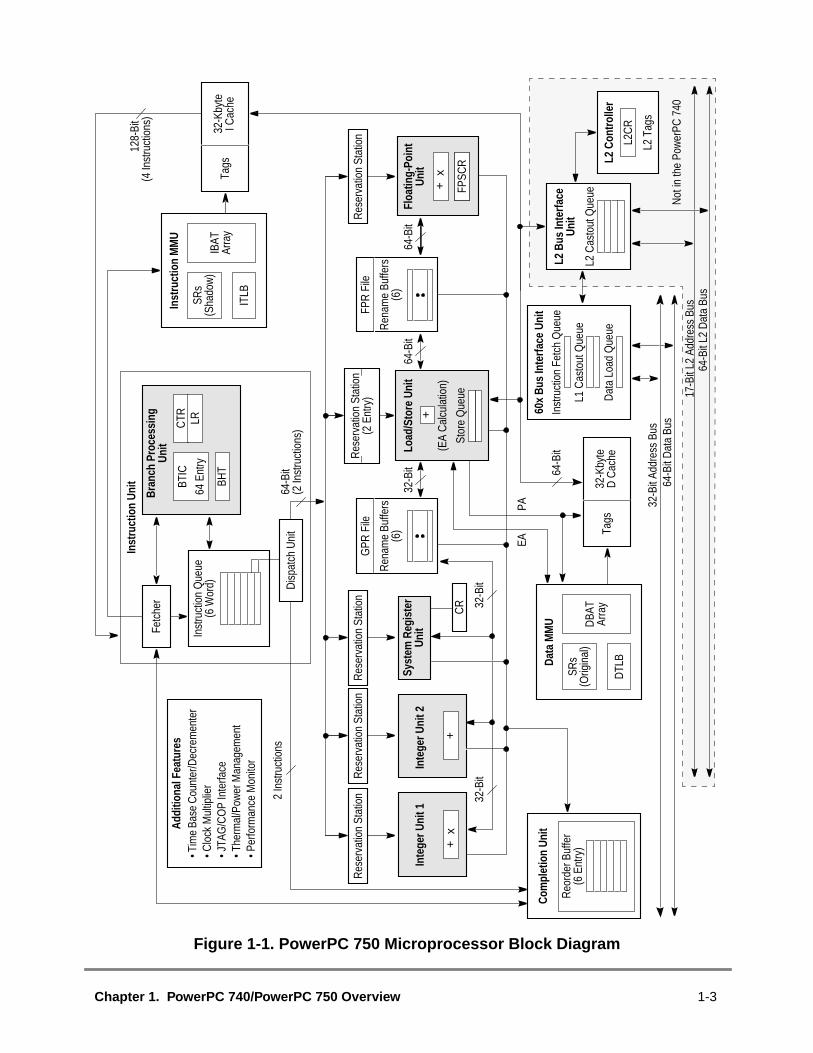
Figure 1-1. PowerPC 750 Microprocessor Block Diagram
Addi
tiona
l Fea
ture
s•T
ime
Base
Cou
nter
/Dec
rem
ente
r• C
lock
Mul
tiplie
r• J
TAG
/CO
P In
terfa
ce• T
herm
al/P
ower
Man
agem
ent
• Per
form
ance
Mon
itor
+
+
Fetc
her
Bran
ch P
roce
ssin
g
BTIC
64 E
ntry
+ x
F
PS
CR
CR
FPSC
R
L2C
R
CTR LR
BHT
Data
MM
U
Inst
ruct
ion
MM
U
Not
in th
e Po
wer
PC 7
40
PAEA
+ x
Inst
ruct
ion
Unit
Unit
Inst
ruct
ion
Que
ue(6
Wor
d)
2 In
stru
ctio
ns
Res
erva
tion
Stat
ion
Res
erva
tion
Stat
ion
Res
erva
tion
Stat
ion
Inte
ger U
nit 1
Syst
em R
egist
erUn
it
Dis
patc
h U
nit
64-B
it(2
Inst
ruct
ions
)
SRs
ITLB
(Sha
dow
)IB
ATAr
ray
32-K
byte
I Cac
heTa
gs
128-
Bit
(4 In
stru
ctio
ns)
Res
erva
tion
Stat
ion
32-B
it
Floa
ting-
Poin
tUn
it
Ren
ame
Buffe
rs(6
)
FPR
File
32-B
it64
-Bit
64-B
it
Res
erva
tion
Stat
ion
(2 E
ntry
)
Load
/Sto
re U
nit
(EA
Cal
cula
tion)
Stor
e Q
ueue
GPR
File
Ren
ame
Buffe
rs(6
)
32-B
it
SRs
(Orig
inal
)
DTL
B
DBA
TAr
ray
64-B
itCo
mpl
etio
n Un
it
Reo
rder
Buf
fer
(6 E
ntry
)
Tags
32-K
byte
D C
ache
60x
Bus
Inte
rface
Uni
tIn
stru
ctio
n Fe
tch
Que
ue
L1 C
asto
ut Q
ueue
Dat
a Lo
ad Q
ueue
L2 C
ontro
ller
L2 T
ags
L2 B
us In
terfa
ceUn
it
L2 C
asto
ut Q
ueue
32-B
it Ad
dres
s Bu
s64
-Bit
Dat
a Bu
s
17-B
it L2
Add
ress
Bus
64-B
it L2
Dat
a Bu
s
Inte
ger U
nit 2
Chapter 1. PowerPC 740/PowerPC 750 Overview 1-3

wn in
lock
he
hedromthe
of
ster
on
1.2 PowerPC 750 Microprocessor FeaturesThis section lists features of the 750. The interrelationship of these features is shoFigure 1-1.
1.2.1 Overview of the PowerPC 750 Microprocessor FeaturesMajor features of the 750 are as follows:
• High-performance, superscalar microprocessor
— As many as four instructions can be fetched from the instruction cache per ccycle
— As many as two instructions can be dispatched per clock
— As many as six instructions can execute per clock (including two integerinstructions)
— Single-clock-cycle execution for most instructions
• Six independent execution units and two register files
— BPU featuring both static and dynamic branch prediction
– 64-entry (16-set, four-way set-associative) branch target instruction cac(BTIC), a cache of branch instructions that have been encountered inbranch/loop code sequences. If a target instruction is in the BTIC, it is fetcinto the instruction queue a cycle sooner than it can be made available fthe instruction cache. Typically, if a fetch access hits the BTIC, it providesfirst two instructions in the target stream.
– 512-entry branch history table (BHT) with two bits per entry for four levelsprediction—not-taken, strongly not-taken, taken, strongly taken
– Branch instructions that do not update the count register (CTR) or link regi(LR) are removed from the instruction stream.
— Two integer units (IUs) that share thirty-two GPRs for integer operands
– IU1 can execute any integer instruction.
– IU2 can execute all integer instructions except multiply and divideinstructions (multiply, divide, shift, rotate, arithmetic, and logicalinstructions). Most instructions that execute in the IU2 take one cycle toexecute. The IU2 has a single-entry reservation station.
— Three-stage FPU
– Fully IEEE 754-1985-compliant FPU for both single- and double-precisioperations
– Supports non-IEEE mode for time-critical operations
– Hardware support for denormalized numbers
– Single-entry reservation station
– Thirty-two 64-bit FPRs for single- or double-precision operands
1-4 IBM PowerPC 740 / PowerPC 750 RISC Microprocessor User’s Manual
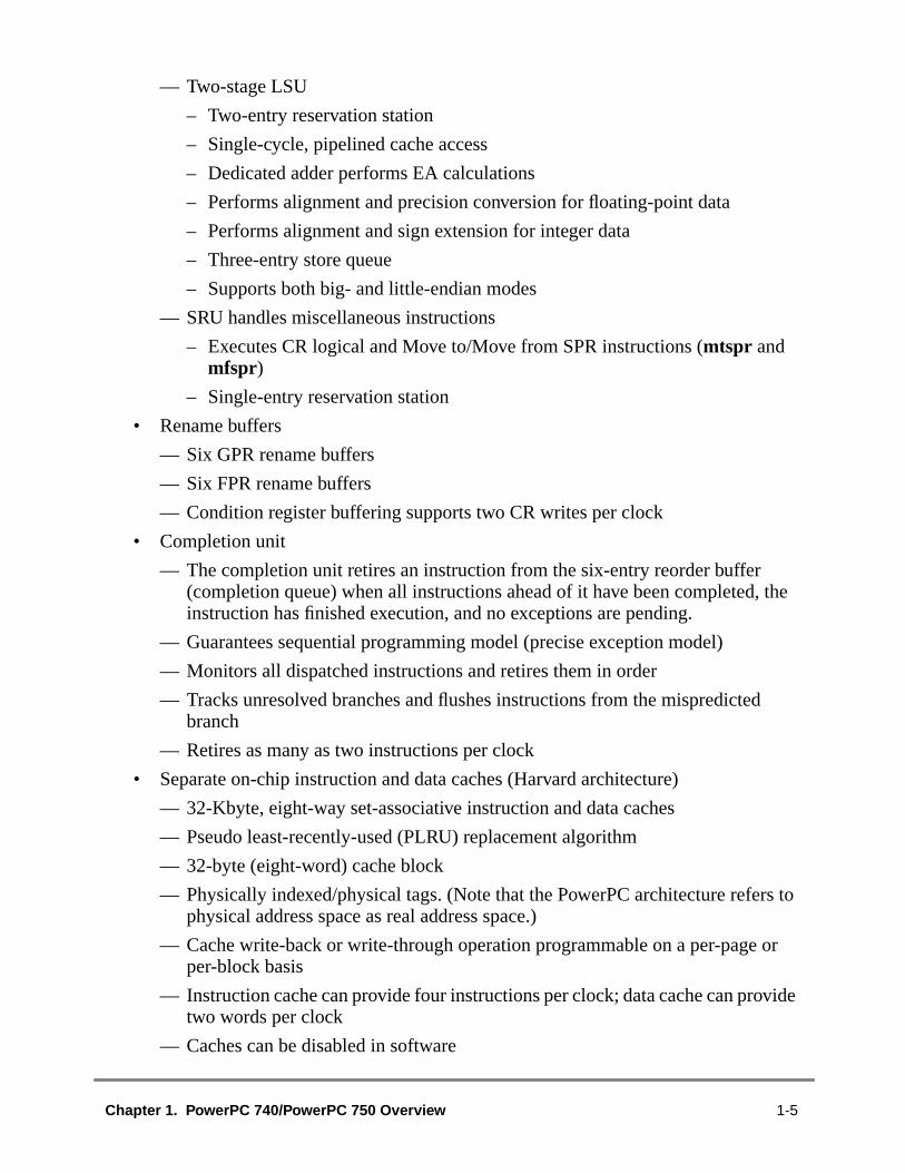
, the
d
rs to
or
vide
— Two-stage LSU
– Two-entry reservation station
– Single-cycle, pipelined cache access
– Dedicated adder performs EA calculations
– Performs alignment and precision conversion for floating-point data
– Performs alignment and sign extension for integer data
– Three-entry store queue
– Supports both big- and little-endian modes
— SRU handles miscellaneous instructions
– Executes CR logical and Move to/Move from SPR instructions (mtspr andmfspr)
– Single-entry reservation station
• Rename buffers
— Six GPR rename buffers
— Six FPR rename buffers
— Condition register buffering supports two CR writes per clock
• Completion unit
— The completion unit retires an instruction from the six-entry reorder buffer(completion queue) when all instructions ahead of it have been completedinstruction has finished execution, and no exceptions are pending.
— Guarantees sequential programming model (precise exception model)
— Monitors all dispatched instructions and retires them in order
— Tracks unresolved branches and flushes instructions from the mispredictebranch
— Retires as many as two instructions per clock
• Separate on-chip instruction and data caches (Harvard architecture)
— 32-Kbyte, eight-way set-associative instruction and data caches
— Pseudo least-recently-used (PLRU) replacement algorithm
— 32-byte (eight-word) cache block
— Physically indexed/physical tags. (Note that the PowerPC architecture refephysical address space as real address space.)
— Cache write-back or write-through operation programmable on a per-pageper-block basis
— Instruction cache can provide four instructions per clock; data cache can protwo words per clock
— Caches can be disabled in software
Chapter 1. PowerPC 740/PowerPC 750 Overview 1-5

ursting
40.)
te
ble,
ent
ed in
x ...
ore
— Caches can be locked in software
— Data cache coherency (MEI) maintained in hardware
— The critical double word is made available to the requesting unit when it is binto the line-fill buffer. The cache is nonblocking, so it can be accessed durthis operation.
• Level 2 (L2) cache interface (The L2 cache interface is not supported in the 7
— On-chip two-way set-associative L2 cache controller and tags
— External data SRAMs
— Support for 256-Kbyte, 512-Kbyte, and 1-Mbyte L2 caches
— 64-byte (256-Kbyte/512-Kbyte) and 128-byte (1 Mbyte) sectored line size
— Supports flow-through (register-buffer), pipelined (register-register), andpipelined late-write (register-register) synchronous burst SRAMs
• Separate memory management units (MMUs) for instructions and data
— 52-bit virtual address; 32-bit physical address
— Address translation for 4-Kbyte pages, variable-sized blocks, and 256-Mbysegments
— Memory programmable as write-back/write-through, cacheable/noncacheaand coherency enforced/coherency not enforced on a page or block basis
— Separate IBATs and DBATs (four each) also defined as SPRs
— Separate instruction and data translation lookaside buffers (TLBs)
– Both TLBs are 128-entry, two-way set associative, and use LRU replacemalgorithm
– TLBs are hardware-reloadable (that is, the page table search is performhardware)
• Separate bus interface units for system memory and for the L2 cache
— Bus interface features include the following:
– Selectable bus-to-core clock frequency ratios of 2x, 2.5x, 3x, 3.5x, 4x, 4.58x. (2x to 8x, all half-clock multipliers in-between)
– A 64-bit, split-transaction external data bus with burst transfers
– Support for address pipelining and limited out-of-order bus transactions
– Single-entry load queue
– Single-entry instruction fetch queue
– Two-entry L1 cache castout queue
– No-DRTRY mode eliminates theDRTRY signal from the qualified bus grant.This allows the forwarding of data during load operations to the internal cone bus cycle sooner than if the use ofDRTRY is enabled.
1-6 IBM PowerPC 740 / PowerPC 750 RISC Microprocessor User’s Manual

the
che.
ustate.
em
tion.
tionntrynextthe
— L2 cache interface features (which are not implemented on the 740) includefollowing:
– Core-to-L2 frequency divisors of 1, 1.5, 2, 2.5, and 3
– Four-entry L2 cache castout queue in L2 cache BIU
– 17-bit address bus
– 64-bit data bus
• Multiprocessing support features include the following:
— Hardware-enforced, three-state cache coherency protocol (MEI) for data ca
— Load/store with reservation instruction pair for atomic memory references,semaphores, and other multiprocessor operations
• Power and thermal management
— Three static modes, doze, nap, and sleep, progressively reduce powerdissipation:
– Doze—All the functional units are disabled except for the timebase/decrementer registers and the bus snooping logic.
– Nap—The nap mode further reduces power consumption by disabling bsnooping, leaving only the time base register and the PLL in a powered s
– Sleep—All internal functional units are disabled, after which external systlogic may disable the PLL and SYSCLK.
— Thermal management facility provides software-controllable thermalmanagement. Thermal management is performed through the use of threesupervisor-level registers and an 750-specific thermal management excep
— Instruction cache throttling provides control of instruction fetching to limitpower consumption.
• Performance monitor can be used to help debug system designs and improvesoftware efficiency.
• In-system testability and debugging features through JTAG boundary-scancapability
1.2.2 Instruction FlowAs shown in Figure 1-1, the 750 instruction unit provides centralized control of instrucflow to the execution units. The instruction unit contains a sequential fetcher, six-einstruction queue (IQ), dispatch unit, and BPU. It determines the address of theinstruction to be fetched based on information from the sequential fetcher and fromBPU.
See Chapter 6, “Instruction Timing,” for a detailed discussion of instruction timing.
Chapter 1. PowerPC 740/PowerPC 750 Overview 1-7

ctionanchecific
tionaken);m the
ranchanchand
andlocktherenchitionscle.unitition isg as
in the6.3.3,
CRfect of
thenchranchn is
The sequential fetcher loads instructions from the instruction cache into the instruqueue. The BPU extracts branch instructions from the sequential fetcher. Brinstructions that cannot be resolved immediately are predicted using either the 750-spdynamic branch prediction or the architecture-defined static branch prediction.
Branch instructions that do not affect the LR or CTR are removed from the instrucstream. The BPU folds branch instructions when a branch is taken (or predicted as tbranch instructions that are not taken, or predicted as not taken, are removed froinstruction stream through the dispatch mechanism.
Instructions issued beyond a predicted branch do not complete execution until the bis resolved, preserving the programming model of sequential execution. If brprediction is incorrect, the instruction unit flushes all predicted path instructions,instructions are fetched from the correct path.
1.2.2.1 Instruction Queue and Dispatch UnitThe instruction queue (IQ), shown in Figure 1-1, holds as many as six instructionsloads up to four instructions from the instruction cache during a single processor ccycle. The instruction fetcher continuously attempts to load as many instructions aswere vacancies in the IQ in the previous clock cycle. All instructions except brainstructions are dispatched to their respective execution units from the bottom two posin the instruction queue (IQ0 and IQ1) at a maximum rate of two instructions per cyReservation stations are provided for the IU1, IU2, FPU, LSU, and SRU. The dispatchchecks for source and destination register dependencies, determines whether a posavailable in the completion queue, and inhibits subsequent instruction dispatchinrequired.
Branch instructions can be detected, decoded, and predicted from anywhereinstruction queue. For a more detailed discussion of instruction dispatch, see Section“Instruction Dispatch and Completion Considerations.”
1.2.2.2 Branch Processing Unit (BPU)The BPU receives branch instructions from the sequential fetcher and performslookahead operations on conditional branches to resolve them early, achieving the efa zero-cycle branch in many cases.
Unconditional branch instructions and conditional branch instructions in whichcondition is known can be resolved immediately. For unresolved conditional brainstructions, the branch path is predicted using either the architecture-defined static bprediction or the 750-specific dynamic branch prediction. Dynamic branch predictioenabled if HID0[BHT] = 1.
1-8 IBM PowerPC 740 / PowerPC 750 RISC Microprocessor User’s Manual

fromtectedon isr and
to bed but
achench
anchctionion isgh thelved.
tered.
musta 64-lly intionthe
locks and
controllatesanchnal tothe
redicatedndent
andd byueue.
them1).
When a prediction is made, instruction fetching, dispatching, and execution continuethe predicted path, but instructions cannot complete and write back results to archiregisters until the prediction is determined to be correct (resolved). When a predictiincorrect, the instructions from the incorrect path are flushed from the processoprocessing begins from the correct path. The 750 allows a second branch instructionpredicted; instructions from the second predicted instruction stream can be fetchecannot be dispatched.
Dynamic prediction is implemented using a 512-entry branch history table (BHT), a cthat provides two bits per entry that together indicate four levels of prediction for a brainstruction—not-taken, strongly not-taken, taken, strongly taken. When dynamic brprediction is disabled, the BPU uses a bit in the instruction encoding to predict the direof the conditional branch. Therefore, when an unresolved conditional branch instructencountered, the 750 executes instructions from the predicted target stream althouresults are not committed to architected registers until the conditional branch is resoThis execution can continue until a second unresolved branch instruction is encoun
When a branch is taken (or predicted as taken), the instructions from the untaken pathbe flushed and the target instruction stream must be fetched into the IQ. The BTIC isentry cache that contains the most recently used branch target instructions, typicapairs. When an instruction fetch hits in the BTIC, the instructions arrive in the instrucqueue in the next clock cycle, a clock cycle sooner than they would arrive frominstruction cache. Additional instructions arrive from the instruction cache in the next ccycle. The BTIC reduces the number of missed opportunities to dispatch instructiongives the processor a one-cycle head start on processing the target stream.
The BPU contains an adder to compute branch target addresses and three user-registers—the link register (LR), the count register (CTR), and the CR. The BPU calcuthe return pointer for subroutine calls and saves it into the LR for certain types of brinstructions. The LR also contains the branch target address for the Branch ConditioLink Register (bclrx) instruction. The CTR contains the branch target address forBranch Conditional to Count Register (bcctrx) instruction. Because the LR and CTR aSPRs, their contents can be copied to or from any GPR. Because the BPU uses deregisters rather than GPRs or FPRs, execution of branch instructions is largely indepefrom execution of integer and floating-point instructions.
1.2.2.3 Completion UnitThe completion unit operates closely with the instruction unit. Instructions are fetcheddispatched in program order. At the point of dispatch, the program order is maintaineassigning each dispatched instruction a successive entry in the six-entry completion qThe completion unit tracks instructions from dispatch through execution and retiresin program order from the two bottom entries in the completion queue (CQ0 and CQ
Chapter 1. PowerPC 740/PowerPC 750 Overview 1-9

in thefrom
s thatranch
FPRs,e 750oves
ction
ing
tegersionctions
it for-zerobunit
nits2-
name
quireo theom themadetion in
Instructions cannot be dispatched to an execution unit unless there is a vacancycompletion queue. Branch instructions that do not update the CTR or LR are removedthe instruction stream and do not take an entry in the completion queue. Instructionupdate the CTR and LR follow the same dispatch and completion procedures as non-binstructions, except that they are not issued to an execution unit.
Completing an instruction commits execution results to architected registers (GPRs,LR, and CTR). In-order completion ensures the correct architectural state when thmust recover from a mispredicted branch or any exception. Retiring an instruction remit from the completion queue.
For a more detailed discussion of instruction completion, see Section 6.3.3, “InstruDispatch and Completion Considerations.”
1.2.2.4 Independent Execution UnitsIn addition to the BPU, the 750 provides the five execution units described in the followsections.
1.2.2.4.1 Integer Units (IUs)The integer units IU1 and IU2 are shown in Figure 1-1. The IU1 can execute any ininstruction; the IU2 can execute any integer instruction except multiplication and diviinstructions. Each IU has a single-entry reservation station that can receive instrufrom the dispatch unit and operands from the GPRs or the rename buffers.
Each IU consists of three single-cycle subunits—a fast adder/comparator, a subunlogical operations, and a subunit for performing rotates, shifts, and count-leadingoperations. These subunits handle all one-cycle arithmetic instructions; only one sucan execute an instruction at a time.
The IU1 has a 32-bit integer multiplier/divider as well as the adder, shift, and logical uof the IU2. The multiplier supports early exit for operations that do not require full 3x
32-bit multiplication.
Each IU has a dedicated result bus (not shown in Figure 1-1) that connects to rebuffers.
1.2.2.4.2 Floating-Point Unit (FPU)The FPU, shown in Figure 1-1, is designed such that single-precision operations reonly a single pass, with a latency of three cycles. As instructions are dispatched tFPU’s reservation station, source operand data can be accessed from the FPRs or frFPR rename buffers. Results in turn are written to the rename buffers and areavailable to subsequent instructions. Instructions pass through the reservation stadispatch order.
1-10 IBM PowerPC 740 / PowerPC 750 RISC Microprocessor User’s Manual

andentble-
ointn for. The-point
NaN,tion
ture
erfaceffectiveg and
somenforceage orte perld intoreslogicstore
cy tonds onthe L2
gicalstem, theavee not
The FPU contains a single-precision multiply-add array and the floating-point statuscontrol register (FPSCR). The multiply-add array allows the 750 to efficiently implemmultiply and multiply-add operations. The FPU is pipelined so that one single- or douprecision instruction can be issued per clock cycle. Thirty-two 64-bit floating-pregisters are provided to support floating-point operations. Stalls due to contentioFPRs are minimized by automatic allocation of the six floating-point rename registers750 writes the contents of the rename registers to the appropriate FPR when floatinginstructions are retired by the completion unit.
The 750 supports all IEEE 754 floating-point data types (normalized, denormalized,zero, and infinity) in hardware, eliminating the latency incurred by software exceproutines. (Note that “exception” is also referred to as “interrupt” in the architecspecification.)
1.2.2.4.3 Load/Store Unit (LSU)The LSU executes all load and store instructions and provides the data transfer intbetween the GPRs, FPRs, and the cache/memory subsystem. The LSU calculates eaddresses, performs data alignment, and provides sequencing for load/store strinmultiple instructions.
Load and store instructions are issued and translated in program order; however,memory accesses can occur out of order. Synchronizing instructions can be used to estrict ordering. When there are no data dependencies and the guarded bit for the pblock is cleared, a maximum of one out-of-order cacheable load operation can execucycle, with a two-cycle total latency on a cache hit. Data returned from the cache is hea rename register until the completion logic commits the value to a GPR or FPR. Scannot be executed out of order and are held in the store queue until the completionsignals that the store operation is to be completed to memory. The 750 executesinstructions with a maximum throughput of one per cycle and a three-cycle total latenthe data cache. The time required to perform the actual load or store operation depethe processor/bus clock ratio and whether the operation involves the on-chip cache,cache, system memory, or an I/O device.
1.2.2.4.4 System Register Unit (SRU)The SRU executes various system-level instructions, as well as condition register looperations and move to/from special-purpose register instructions. To maintain systate, most instructions executed by the SRU are execution-serialized; that isinstruction is held for execution in the SRU until all previously issued instructions hexecuted. Results from execution-serialized instructions executed by the SRU aravailable or forwarded for subsequent instructions until the instruction completes.
Chapter 1. PowerPC 740/PowerPC 750 Overview 1-11

s forintained
n unitctive
n therentical
ge size
o 256
f thet aren-chipAftercache
ss in theslated
ry unit
cess, anlationrrayle to
hes for
achearedress
te andicallyaded
1.2.3 Memory Management Units (MMUs)The 750’s MMUs support up to 4 Petabytes (252) of virtual memory and 4 Gigabytes (232)of physical memory for instructions and data. The MMUs also control access privilegethese spaces on block and page granularities. Referenced and changed status is maby the processor for each page to support demand-paged virtual memory systems.
The LSU calculates effective addresses for data loads and stores; the instructiocalculates effective addresses for instruction fetching. The MMU translates the effeaddress to determine the correct physical address for the memory access.
The 750 supports the following types of memory translation:
• Real addressing mode—In this mode, translation is disabled by clearing bits imachine state register (MSR): MSR[IR] for instruction fetching or MSR[DR] fodata accesses. When address translation is disabled, the physical address is idto the effective address.
• Page address translation—translates the page frame address for a 4-Kbyte pa
• Block address translation—translates the base address for blocks (128 Kbytes tMbytes)
If translation is enabled, the appropriate MMU translates the higher-order bits oeffective address into physical address bits. The lower-order address bits (thauntranslated and therefore, considered both logical and physical) are directed to the ocaches where they form the index into the eight-way set-associative tag array.translating the address, the MMU passes the higher-order physical address bits to theand the cache lookup completes. For caching-inhibited accesses or accesses that micache, the untranslated lower-order address bits are concatenated with the tranhigher-order address bits; the resulting 32-bit physical address is used by the memoand the system interface, which accesses external memory.
The TLBs store page address translations for recent memory accesses. For each aceffective address is presented for page and block translation simultaneously. If a transis found in both the TLB and the BAT array, the block address translation in the BAT ais used. Usually the translation is in a TLB and the physical address is readily availabthe on-chip cache. When a page address translation is not in a TLB, hardware searcone in the page table following the model defined by the PowerPC architecture.
Instruction and data TLBs provide address translation in parallel with the on-chip caccess, incurring no additional time penalty in the event of a TLB hit. The 750’s TLBs128-entry, two-way set-associative caches that contain instruction and data adtranslations. The 750 automatically generates a TLB search on a TLB miss.
1.2.4 On-Chip Instruction and Data CachesThe 750 implements separate instruction and data caches. Each cache is 32-Kbyeight-way set associative. As defined by the PowerPC architecture, they are physindexed. Each cache block contains eight contiguous words from memory that are lo
1-12 IBM PowerPC 740 / PowerPC 750 RISC Microprocessor User’s Manual

evert load.hes are. Thethe
cache
the-blockettingcheags areesourcethe
tion. Thettingon
from an 8-word boundary (that is, bits EA[27–31] are zeros); thus, a cache block ncrosses a page boundary. An entire cache block can be updated by a four-beat bursMisaligned accesses across a page boundary can incur a performance penalty. Cacnonblocking, write-back caches with hardware support for reloading on cache missescritical double word is transferred on the first beat and is simultaneously written tocache and forwarded to the requesting unit, minimizing stalls due to load delays. Thebeing loaded is not blocked to internal accesses while the load completes.
The 750 cache organization is shown in Figure 1-2.
Figure 1-2. Cache Organization
Within one cycle, the data cache provides double-word access to the LSU. Likeinstruction cache, the data cache can be invalidated all at once or on a per-cachebasis. The data cache can be disabled and invalidated by clearing HID0[DCE] and sHID0[DCFI]. The data cache can be locked by setting HID0[DLOCK]. To ensure cacoherency, the data cache supports the three-state MEI protocol. The data cache tsingle-ported, so a simultaneous load or store and a snoop access represent a rcollision. If a snoop hit occurs, the LSU is blocked internally for one cycle to alloweight-word block of data to be copied to the write-back buffer.
Within one cycle, the instruction cache provides up to four instructions to the instrucqueue. The instruction cache can be invalidated entirely or on a cache-block basisinstruction cache can be disabled and invalidated by clearing HID0[ICE] and seHID0[ICFI]. The instruction cache can be locked by setting HID0[ILOCK]. The instructicache supports only the valid/invalid states.
8 Words/Way
128 Sets
Way 5
Way 6
Way 7
Way 4 Address Tag 4
Address Tag 5
Address Tag 6
Address Tag 7
Way 1
Way 2
Way 3
Way 0 Address Tag 0
Address Tag 1
Address Tag 2
Address Tag 3
State
State
State
Words [0–7]
State
Words [0–7]
Words [0–7]
Words [0–7]
State
State
State
Words [0–7]
State
Words [0–7]
Words [0–7]
Words [0–7]
Chapter 1. PowerPC 740/PowerPC 750 Overview 1-13

targetbeen, it ism theam.
s, see
uction-way,
e. Thele bankack
turncy is
bitstheages-byte
storethe L1
y are
he cannd twore aree nextiority
ut toBGA
The 750 also implements a 64-entry (16-set, four-way set-associative) branchinstruction cache (BTIC). The BTIC is a cache of branch instructions that haveencountered in branch/loop code sequences. If the target instruction is in the BTICfetched into the instruction queue a cycle sooner than it can be made available froinstruction cache. Typically the BTIC contains the first two instructions in the target streThe BTIC can be disabled and invalidated through software.
For more information and timing examples showing cache hit and cache miss latencieSection 6.3.2, “Instruction Fetch Timing.”
1.2.5 L2 Cache Implementation (Not Supported in the PowerPC 740)The L2 cache is a unified cache that receives memory requests from both the L1 instrand data caches independently. The L2 cache is implemented with an on-chip, twoset-associative tag memory, and with external, synchronous SRAMs for data storagexternal SRAMs are accessed through a dedicated L2 cache port that supports a singof up to 1 Mbyte of synchronous SRAMs. The L2 cache normally operates in write-bmode and supports system cache coherency through snooping.
Depending on its size, the L2 cache is organized into 64- or 128-byte lines, which inare subdivided into 32-byte sectors (blocks), the unit at which cache coherenmaintained.
The L2 cache controller contains the L2 cache control register (L2CR), which includesfor enabling parity checking, setting the L2-to-processor clock ratio, and identifyingtype of RAM used for the L2 cache implementation. The L2 cache controller also manthe L2 cache tag array, two-way set-associative with 4K tags per way. Each sector (32cache block) has its own valid and modified status bits.
Requests from the L1 cache generally result from instruction misses, data load ormisses, write-through operations, or cache management instructions. Requests fromcache are looked up in the L2 tags and serviced by the L2 cache if they hit; theforwarded to the bus interface if they miss.
The L2 cache can accept multiple, simultaneous accesses. The L1 instruction cacrequest an instruction at the same time that the L1 data cache is requesting one load astore operations. The L2 cache also services snoop requests from the bus. If themultiple pending requests to the L2 cache, snoop requests have highest priority. Thpriority consists of load and store requests from the L1 data cache. The next prconsists of instruction fetch requests from the L1 instruction cache.
For more information, see Chapter 9, “L2 Cache Interface Operation.”
The L2 cache interface is physically present in the 740, but the IOs are not brought othe package. Initially, the 740 uses a 255 pin CBGA package; the 750 uses a 360 pin Cpackage.
1-14 IBM PowerPC 740 / PowerPC 750 RISC Microprocessor User’s Manual

memoryary
essor
4, 32,eableis
nsfer
burst-ed byh)
e-beatat arehits a
trolled
m thatible,
d bus
ludingthey750exists,
a writesnoopthe 750
e is
g andcontrol
1.2.6 System Interface/Bus Interface Unit (BIU)The address and data buses operate independently; address and data tenures of aaccess are decoupled to provide a more flexible control of memory traffic. The primactivity of the system interface is transferring data and instructions between the procand system memory. There are two types of memory accesses:
• Single-beat transfers—These memory accesses allow transfer sizes of 8, 16, 2or 64 bits in one bus clock cycle. Single-beat transactions are caused by uncachread and write operations that access memory directly (that is, when caching disabled), cache-inhibited accesses, and stores in write-through mode.
• Four-beat burst (32 bytes) data transfers—Burst transactions, which always traan entire cache block (32 bytes), are initiated when an entire cache block istransferred. Because the first-level caches on the 750 are write-back caches, read memory, burst operations are the most common memory accesses, followburst-write memory operations, and single-beat (noncacheable or write-througmemory read and write operations.
The 750 also supports address-only operations, variants of the burst and singloperations, (for example, atomic memory operations and global memory operations thsnooped), and address retry activity (for example, when a snooped read accessmodified block in the cache). The broadcast of some address-only operations is conthrough HID0[ABE]. I/O accesses use the same protocol as memory accesses.
Access to the system interface is granted through an external arbitration mechanisallows devices to compete for bus mastership. This arbitration mechanism is flexallowing the 750 to be integrated into systems that implement various fairness anparking procedures to avoid arbitration overhead.
Typically, memory accesses are weakly ordered—sequences of operations, incload/store string and multiple instructions, do not necessarily complete in the orderbegin—maximizing the efficiency of the bus without sacrificing data coherency. Theallows read operations to go ahead of store operations (except when a dependencyor in cases where a noncacheable access is performed), and provides support foroperation to go ahead of a previously queued read data tenure (for example, letting apush be enveloped between address and data tenures of a read operation). Becausecan dynamically optimize run-time ordering of load/store traffic, overall performancimproved.
The system interface is specific for each PowerPC microprocessor implementation.
The 750 signals are grouped as shown in Figure 1-3. Signals are provided for clockincontrol of the L2 caches, as well as separate L2 address and data buses. Test andsignals provide diagnostics for selected internal circuits.
Chapter 1. PowerPC 740/PowerPC 750 Overview 1-15

of oneds on
tionsof the
busother
s bus
paritye
fe-
of thes that
parityr.
Figure 1-3. System Interface
The system interface supports address pipelining, which allows the address tenuretransaction to overlap the data tenure of another. The extent of the pipelining depenexternal arbitration and control circuitry. Similarly, the 750 supports split-bus transacfor systems with multiple potential bus masters—one device can have mastershipaddress bus while another has mastership of the data bus. Allowing multipletransactions to occur simultaneously increases the available bus bandwidth foractivity.
The 750’s clocking structure supports a wide range of processor-to-bus clock ratios.
1.2.7 SignalsThe 750’s signals are grouped as follows:
• Address arbitration signals—The 750 uses these signals to arbitrate for addresmastership.
• Address start signals—These signals indicate that a bus master has begun atransaction on the address bus.
• Address transfer signals—These signals include the address bus and addresssignals. They are used to transfer the address and to ensure the integrity of thtransfer.
• Transfer attribute signals—These signals provide information about the type otransfer, such as the transfer size and whether the transaction is bursted, writthrough, or caching-inhibited.
• Address termination signals—These signals are used to acknowledge the endaddress phase of the transaction. They also indicate whether a condition existrequires the address phase to be repeated.
• Data arbitration signals—The 750 uses these signals to arbitrate for data busmastership.
• Data transfer signals—These signals, which consist of the data bus and data signals, are used to transfer the data and to ensure the integrity of the transfe
Address Arbitration
Address Start
Address Transfer
Transfer Attribute
Address Termination
Clocks
Data Arbitration
Data Transfer
Data Termination
Processor Status/Control
Test and Control
L2 Cache Address/Data1
L2 Cache Clock/Control1
System Status
VDD VDD (I/O)
750
1 Not supported in the 740
1-16 IBM PowerPC 740 / PowerPC 750 RISC Microprocessor User’s Manual

beatcatesidualsod.
the
cessing
, anderrupt
on
urces
ides
gnals
• Data termination signals—Data termination signals are required after each datain a data transfer. In a single-beat transaction, a data termination signal also indithe end of the tenure; in burst accesses, data termination signals apply to indivbeats and indicate the end of the tenure only after the final data beat. They alindicate whether a condition exists that requires the data phase to be repeate
• L2 cache clock/control signals—These signals provide clocking and control forL2 cache. (Not supported in the 740.)
• L2 cache address/data—The 750 has separate address and data buses for acthe L2 cache. (Not supported in the 740.)
• Interrupt signals—These signals include the interrupt signal, checkstop signalsboth soft reset and hard reset signals. These signals are used to generate intexceptions and, under various conditions, to reset the processor.
• Processor status/control signals—These signals are used to set the reservaticoherency bit, enable the time base, and other functions.
• Miscellaneous signals—These signals are used in conjunction with such resoas secondary caches and the time base facility.
• JTAG/COP interface signals—The common on-chip processor (COP) unit prova serial interface to the system for performing board-level boundary scaninterconnect tests.
• Clock signals—These signals determine the system clock frequency. These sican also be used to synchronize multiprocessor systems.
NOTEA bar over a signal name indicates that the signal is activelow—for example,ARTRY (address retry) andTS (transferstart). Active-low signals are referred to as asserted (active)when they are low and negated when they are high. Signals thatare not active low, such as AP[0–3] (address bus parity signals)and TT[0–4] (transfer type signals) are referred to as assertedwhen they are high and negated when they are low.
Chapter 1. PowerPC 740/PowerPC 750 Overview 1-17

ction.
nd
1.2.8 Signal ConfigurationFigure 1-4 shows the 750's logical pin configuration. The signals are grouped by fun
Figure 1-4. PowerPC 750 Microprocessor Signal Groups
Signal functionality is described in detail in Chapter 7, “Signal Descriptions,” aChapter 8, “Bus Interface Operation.”
DataArbitration
L2 CacheAddress/Data
BRBG
ABB
TS
AP[0–3]
GBL
TSIZ[0–2]
AACK
ARTRY
SYSCLK
DBG
DBWO
DBB
D[0–63]
DP[0–7]
TADRTRY
TEA
INT
JTAG/COP
Factory Test
1
1
1
1
1
5
3
4
TBST
WT
PLL_CFG[0–3]
TT[0–4]5
4
TBEN
1CLK_OUT
MCP
SRESET
TLBISYNC
L2ADDR[16–0]
SMI
HRESET
QREQ
QACK
CKSTP_IN
CKSTP_OUT
L2DATA[0–63]
L2DP[0–7]
L2CEL2WEL2CLK_OUT[A–B]
1
3
1
1
1
1
1
1
1
8
64
1
1
1
1
1
1
1
1
1
1
1
1
1
1
1
CI 1
A[0–31]32
L2SYNC_OUT
AddressArbitration
AddressBus
L2SYNC_IN
L2ZZ
L2 CacheClock/Control
AddressTermination
AddressStart
TransferAttributes
DataTransfer
DataTermination
Interrupts/Resets
ProcessorStatus/Control
VDD VDD (I/O)
ClockControl
TestInterface
RSRV
17
2
1
1
1
64
8
1
1
L2VDD
L2AVDD
750
DBDIS1
AVDD
Not supported inthe PowerPC 740
1-18 IBM PowerPC 740 / PowerPC 750 RISC Microprocessor User’s Manual

rfacerate aput.
theTheclock,he PLL
ratioss islock
ances theTheo take
out thessorach
mingon in
s the
sin
ibesal
1.2.9 ClockingThe 750 requires a single system clock input, SYSCLK, that represents the bus intefrequency. Internally, the processor uses a phase-locked loop (PLL) circuit to genemaster core clock that is frequency-multiplied and phase-locked to the SYSCLK inThis core frequency is used to operate the internal circuitry.
The PLL is configured by the PLL_CFG[0–3] signals, which select the multiplier thatPLL uses to multiply the SYSCLK frequency up to the internal core frequency.feedback in the PLL guarantees that the processor clock is phase locked to the busregardless of process variations, temperature changes, or parasitic capacitances. Talso ensures a 50% duty cycle for the processor clock.
The 750 supports various processor-to-bus clock frequency ratios, although not allare available for all frequencies. Configuration of the processor/bus clock ratiodisplayed through a 750-specific register, HID1. For information about supported cfrequencies, see the 750 hardware specifications.
1.3 PowerPC 750 Microprocessor: ImplementationThe PowerPC architecture is derived from the POWER architecture (PerformOptimized with Enhanced RISC architecture). The PowerPC architecture sharebenefits of the POWER architecture optimized for single-chip implementations.PowerPC architecture design facilitates parallel instruction execution and is scalable tadvantage of future technological gains.
This section describes the PowerPC architecture in general, and specific details abimplementation of the 750 as a low-power, 32-bit member of the PowerPC procefamily. The structure of this section follows the organization of the user’s manual; esubsection provides an overview of each chapter.
• Registers and programming model—Section 1.4, “PowerPC Registers andProgramming Model,” describes the registers for the operating environmentarchitecture common among PowerPC processors and describes the programmodel. It also describes the registers that are unique to the 750. The informatithis section is described more fully in Chapter 2, “Programming Model.”
• Instruction set and addressing modes—Section 1.5, “Instruction Set,” describePowerPC instruction set and addressing modes for the PowerPC operatingenvironment architecture, and defines and describes the PowerPC instructionimplemented in the 750. The information in this section is described more fullyChapter 2, “Programming Model.”
• Cache implementation—Section 1.6, “On-Chip Cache Implementation,” descrthe cache model that is defined generally for PowerPC processors by the virtuenvironment architecture. It also provides specific details about the 750 cacheimplementation. The information in this section is described more fully inChapter 3, “Instruction and Data Cache Operation.”
Chapter 1. PowerPC 740/PowerPC 750 Overview 1-19

del 750
allyhisryy in
tionction
ower or
the
eding-ms thisent.”
,
t are
• Exception model—Section 1.7, “Exception Model,” describes the exception moof the PowerPC operating environment architecture and the differences in theexception model. The information in this section is described more fully inChapter 4, “Exceptions.”
• Memory management—Section 1.8, “Memory Management,” describes generthe conventions for memory management among the PowerPC processors. Tsection also describes the 750’s implementation of the 32-bit PowerPC memomanagement specification. The information in this section is described more fullChapter 5, “Memory Management.”
• Instruction timing—Section 1.9, “Instruction Timing,” provides a generaldescription of the instruction timing provided by the superscalar, parallel execusupported by the PowerPC architecture and the 750. The information in this seis described more fully in Chapter 6, “Instruction Timing.”
• Power management—Section 1.10, “Power Management,” describes how the pmanagement can be used to reduce power consumption when the processor,portions of it, are idle. The information in this section is described more fully inChapter 10, “Power and Thermal Management.”
• Thermal management—Section 1.11, “Thermal Management,” describes howthermal management unit and its associated registers (THRM1–THRM3) andexception can be used to manage system activity in a way that prevents excesystem and junction temperature thresholds. This is particularly useful in highperformance portable systems, which cannot use the same cooling mechanis(such as fans) that control overheating in desktop systems. The information insection is described more fully in Chapter 10, “Power and Thermal Managem
• Performance monitor—Section 1.12, “Performance Monitor,” describes theperformance monitor facility, which system designers can use to help bring updebug, and optimize software performance. The information in this section isdescribed more fully in Chapter 11, “Performance Monitor.”
The following sections summarize the features of the 750, distinguishing those thadefined by the architecture from those that are unique to the 750 implementation.
1-20 IBM PowerPC 740 / PowerPC 750 RISC Microprocessor User’s Manual

erPCture
el, a
delribesA
, and the
he andof thee, see
ssor
tionalor are
gisterrce
icallycationrposesor also
ratingtingof theted only
The PowerPC architecture consists of the following layers, and adherence to the Powarchitecture can be described in terms of which of the following levels of the architecis implemented:
• PowerPC user instruction set architecture (UISA)—Defines the base user-levinstruction set, user-level registers, data types, floating-point exception modelmemory models for a uniprocessor environment, and programming model foruniprocessor environment.
• PowerPC virtual environment architecture (VEA)—Describes the memory mofor a multiprocessor environment, defines cache control instructions, and descother aspects of virtual environments. Implementations that conform to the VEalso adhere to the UISA, but may not necessarily adhere to the OEA.
• PowerPC operating environment architecture (OEA)—Defines the memorymanagement model, supervisor-level registers, synchronization requirementsthe exception model. Implementations that conform to the OEA also adhere toUISA and the VEA.
The PowerPC architecture allows a wide range of designs for such features as cacsystem interface implementations. The 750 implementations support the three levelsarchitecture described above. For more information about the PowerPC architecturPowerPC Microprocessor Family: The Programming Environments.
Specific features of the 750 are listed in Section 1.2, “PowerPC 750 MicroproceFeatures.”
1.4 PowerPC Registers and Programming ModelThe PowerPC architecture defines register-to-register operations for most computainstructions. Source operands for these instructions are accessed from the registersprovided as immediate values embedded in the instruction opcode. The three-reinstruction format allows specification of a target register distinct from the two souoperands. Load and store instructions transfer data between registers and memory.
PowerPC processors have two levels of privilege—supervisor mode of operation (typused by the operating system) and user mode of operation (used by the applisoftware). The programming models incorporate 32 GPRs, 32 FPRs, special-puregisters (SPRs), and several miscellaneous registers. Each PowerPC microproceshas its own unique set of hardware implementation-dependent (HID) registers.
Having access to privileged instructions, registers, and other resources allows the opesystem to control the application environment (providing virtual memory and protecoperating-system and critical machine resources). Instructions that control the stateprocessor, the address translation mechanism, and supervisor registers can be execuwhen the processor is operating in supervisor mode.
Chapter 1. PowerPC 740/PowerPC 750 Overview 1-21

. Thef the
Figure 1-5 shows all the 750 registers available at the user and supervisor levelnumbers to the right of the SPRs indicate the number that is used in the syntax oinstruction operands to access the register.
For more information, see Chapter 2, “Programming Model.”
1-22 IBM PowerPC 740 / PowerPC 750 RISC Microprocessor User’s Manual

Figure 1-5. PowerPC 750 Microprocessor Programming Model—Registers
ICTC SPR 1019SPR 1020
SPR 1021
SPR 1022
THRM1
THRM2
THRM3
SPR 937
SPR 938
SPR 941
SPR 942
PerformanceCounters 1
SampledInstructionAddress 1
DSISR
Data AddressRegister
SPRGs
Exception Handling RegistersSave and RestoreRegisters
Instruction BATRegisters
Data BATRegisters
Memory Management Registers
Machine StateRegister
MSR
ProcessorVersionRegister
SPR 287PVR
Configuration RegistersHardwareImplementationRegisters 1
SPR 1
USER MODEL—UISA
Floating-PointStatus and
Control Register
FPSCR
ConditionRegister
General-PurposeRegisters
XER
XER
SPR 8
Link Register
LR
SUPERVISOR MODEL—OEA
DecrementerExternal AccessRegister
EAR
SDR1
SPR 9
CountRegister
Miscellaneous Registers
SegmentRegisters
1These registers are 750-specific registers. They may not be supported by other PowerPC processors.
CR
Floating-PointRegistersPerformance
Monitor Registers(For Reading)
Performance Counters 1
Monitor Control 1
SPR 939USIA
Sampled InstructionAddress 1
Performance Monitor Registers
Monitor Control 1
Time Base(For Writing)
Power/Thermal Management RegistersThermal AssistUnit Registers 1
Instruction CacheThrottling ControlRegister 1
USER MODEL—VEA
TBL TBR 268
Time Base Facility (For Reading)
CTR
2Not supported by the 740.
GPR0
GPR1
GPR31
TBU TBR 269
IBAT0U
IBAT0L
IBAT1U
IBAT1L
IBAT2U
IBAT2L
IBAT3U
IBAT3L
SPR 528
SPR 529
SPR 530
SPR 531
SPR 532
SPR 533
SPR 534
SPR 535
SPR 536
SPR 537
SPR 538
SPR 539
SPR 540
SPR 541
SPR 542
SPR 543
DBAT0U
DBAT0L
DBAT1U
DBAT1L
DBAT2U
DBAT2L
DBAT3U
DBAT3L
SR0
SR1
SR15
SDR1 SPR 25
HID0
HID1
SPR 1008
SPR 1009
FPR0
FPR1
FPR31
UPMC1
UPMC2
UPMC3
UPMC4
UMMCR0
UMMCR1
SPR 936
SPR 940
SPR 953
SPR 954
SPR 957
SPR 958
PMC1
PMC2
PMC3
PMC4
SIA SPR 955
MMCR0
MMCR1
SPR 952
SPR 956
SPRG0
SPRG1
SPRG2
SPRG3
SPR 272
SPR 273
SPR 274
SPR 275
DAR
DSISR
SPR 19
SPR 18
SRR0 SPR 26
SRR1 SPR 27
SPR 282 TBL SPR 284
TBU SPR 285
DEC SPR 22
Data AddressBreakpoint Register
DABR SPR 1013
L2 ControlRegister 1, 2
L2CR SPR 1017
Instruction AddressBreakpoint Register 1
IABR SPR 1010
Chapter 1. PowerPC 740/PowerPC 750 Overview 1-23
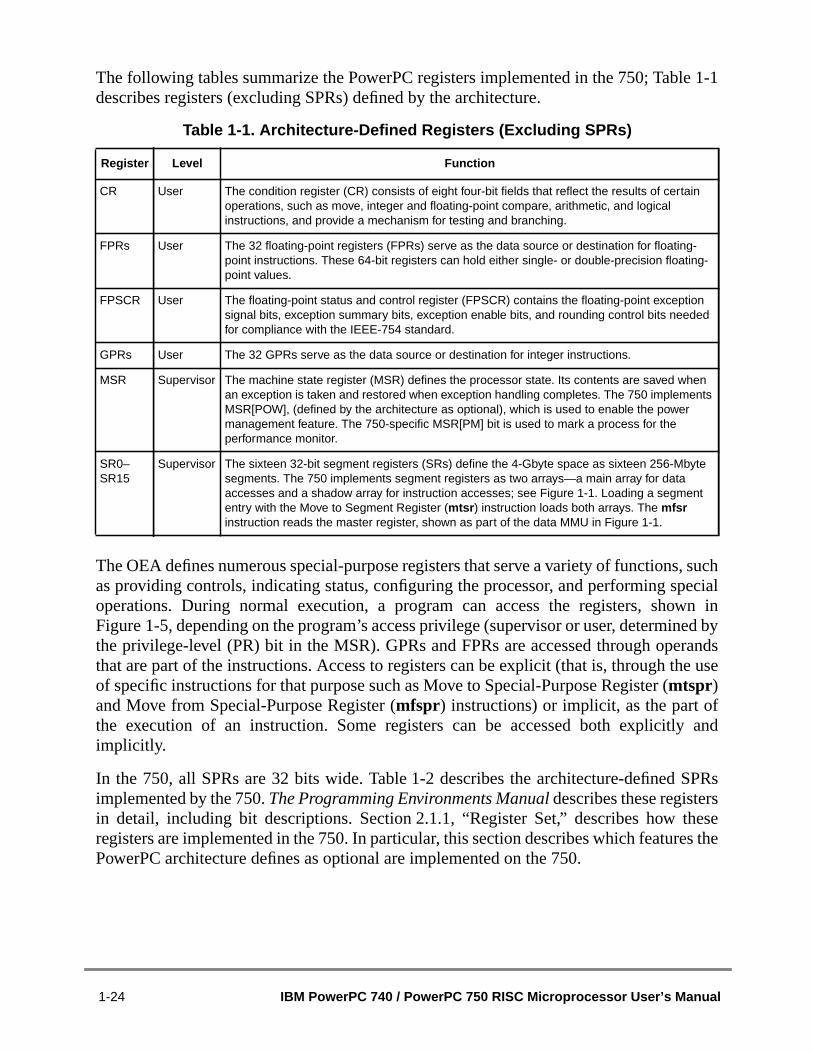
le 1-1
, suchecial
wn ined byrandse use
fand
SPRsshesees the
The following tables summarize the PowerPC registers implemented in the 750; Tabdescribes registers (excluding SPRs) defined by the architecture.
The OEA defines numerous special-purpose registers that serve a variety of functionsas providing controls, indicating status, configuring the processor, and performing spoperations. During normal execution, a program can access the registers, shoFigure 1-5, depending on the program’s access privilege (supervisor or user, determinthe privilege-level (PR) bit in the MSR). GPRs and FPRs are accessed through opethat are part of the instructions. Access to registers can be explicit (that is, through thof specific instructions for that purpose such as Move to Special-Purpose Register (mtspr)and Move from Special-Purpose Register (mfspr) instructions) or implicit, as the part othe execution of an instruction. Some registers can be accessed both explicitlyimplicitly.
In the 750, all SPRs are 32 bits wide. Table 1-2 describes the architecture-definedimplemented by the 750.The Programming Environments Manualdescribes these registerin detail, including bit descriptions. Section 2.1.1, “Register Set,” describes how tregisters are implemented in the 750. In particular, this section describes which featurPowerPC architecture defines as optional are implemented on the 750.
Table 1-1. Architecture-Defined Registers (Excluding SPRs)
Register Level Function
CR User The condition register (CR) consists of eight four-bit fields that reflect the results of certainoperations, such as move, integer and floating-point compare, arithmetic, and logicalinstructions, and provide a mechanism for testing and branching.
FPRs User The 32 floating-point registers (FPRs) serve as the data source or destination for floating-point instructions. These 64-bit registers can hold either single- or double-precision floating-point values.
FPSCR User The floating-point status and control register (FPSCR) contains the floating-point exceptionsignal bits, exception summary bits, exception enable bits, and rounding control bits neededfor compliance with the IEEE-754 standard.
GPRs User The 32 GPRs serve as the data source or destination for integer instructions.
MSR Supervisor The machine state register (MSR) defines the processor state. Its contents are saved whenan exception is taken and restored when exception handling completes. The 750 implementsMSR[POW], (defined by the architecture as optional), which is used to enable the powermanagement feature. The 750-specific MSR[PM] bit is used to mark a process for theperformance monitor.
SR0–SR15
Supervisor The sixteen 32-bit segment registers (SRs) define the 4-Gbyte space as sixteen 256-Mbytesegments. The 750 implements segment registers as two arrays—a main array for dataaccesses and a shadow array for instruction accesses; see Figure 1-1. Loading a segmententry with the Move to Segment Register (mtsr ) instruction loads both arrays. The mfsrinstruction reads the master register, shown as part of the data MMU in Figure 1-1.
1-24 IBM PowerPC 740 / PowerPC 750 RISC Microprocessor User’s Manual

y thetailed
Table 1-3 describes the supervisor-level SPRs in the 750 that are not defined bPowerPC architecture. Section 2.1.2, “PowerPC 750-Specific Registers,” gives dedescriptions of these registers, including bit descriptions.
Table 1-2. Architecture-Defined SPRs Implemented
Register Level Function
LR User The link register (LR) can be used to provide the branch target address and to hold thereturn address after branch and link instructions.
BATs Supervisor The architecture defines 16 block address translation registers (BATs), which operate inpairs. There are four pairs of data BATs (DBATs) and four pairs of instruction BATs(IBATs). BATs are used to define and configure blocks of memory.
CTR User The count register (CTR) is decremented and tested by branch-and-count instructions.
DABR Supervisor The optional data address breakpoint register (DABR) supports the data addressbreakpoint facility.
DAR User The data address register (DAR) holds the address of an access after an alignment or DSIexception.
DEC Supervisor The decrementer register (DEC) is a 32-bit decrementing counter that provides a way toschedule decrementer exceptions.
DSISR User The DSISR defines the cause of data access and alignment exceptions.
EAR Supervisor The external access register (EAR) controls access to the external access facility throughthe External Control In Word Indexed (eciwx ) and External Control Out Word Indexed(ecowx ) instructions.
PVR Supervisor The processor version register (PVR) is a read-only register that identifies the processor.
SDR1 Supervisor SDR1 specifies the page table format used in virtual-to-physical page address translation.
SRR0 Supervisor The machine status save/restore register 0 (SRR0) saves the address used for restartingan interrupted program when a Return from Interrupt (rfi ) instruction executes.
SRR1 Supervisor The machine status save/restore register 1 (SRR1) is used to save machine status onexceptions and to restore machine status when an rfi instruction is executed.
SPRG0–SPRG3
Supervisor SPRG0–SPRG3 are provided for operating system use.
TB User: readSupervisor:read/write
The time base register (TB) is a 64-bit register that maintains the time of day and operatesinterval timers. The TB consists of two 32-bit fields—time base upper (TBU) and time baselower (TBL).
XER User The XER contains the summary overflow bit, integer carry bit, overflow bit, and a fieldspecifying the number of bytes to be transferred by a Load String Word Indexed (lswx ) orStore String Word Indexed (stswx ) instruction.
Chapter 1. PowerPC 740/PowerPC 750 Overview 1-25

matsralleleatly
1.5 Instruction SetAll PowerPC instructions are encoded as single-word (32-bit) opcodes. Instruction forare consistent among all instruction types, permitting efficient decoding to occur in pawith operand accesses. This fixed instruction length and consistent format grsimplifies instruction pipelining.
For more information, see Chapter 2, “Programming Model.”
Table 1-3. Implementation-Specific Registers
Register Level Function
HID0 Supervisor The hardware implementation-dependent register 0 (HID0) provides checkstop enablesand other functions.
HID1 Supervisor The hardware implementation-dependent register 1 (HID1) allows software to read theconfiguration of the PLL configuration signals.
IABR Supervisor The instruction address breakpoint register (IABR) supports instruction addressbreakpoint exceptions. It can hold an address to compare with instruction addresses inthe IQ. An address match causes an instruction address breakpoint exception.
ICTC Supervisor The instruction cache-throttling control register (ICTC) has bits for controlling the intervalat which instructions are fetched into the instruction buffer in the instruction unit. Thishelps control the 750’s overall junction temperature.
L2CR Supervisor The L2 cache control register (L2CR) is used to configure and operate the L2 cache. Ithas bits for enabling parity checking, setting the L2-to-processor clock ratio, andidentifying the type of RAM used for the L2 cache implementation. (The L2 cache featureis not supported in the 740.)
MMCR0–MMCR1
Supervisor The monitor mode control registers (MMCR0–MMCR1) are used to enable variousperformance monitoring interrupt functions. UMMCR0–UMMCR1 provide user-level readaccess to MMCR0–MMCR1.
PMC1–PMC4
Supervisor The performance monitor counter registers (PMC1–PMC4) are used to count specifiedevents. UPMC1–UPMC4 provide user-level read access to these registers.
SIA Supervisor The sampled instruction address register (SIA) holds the EA of an instruction executingat or around the time the processor signals the performance monitor interrupt condition.The USIA register provides user-level read access to the SIA.
THRM1,THRM2
Supervisor THRM1 and THRM2 provide a way to compare the junction temperature against twouser-provided thresholds. The thermal assist unit (TAU) can be operated so that thethermal sensor output is compared to only one threshold, selected in THRM1 or THRM2.
THRM3 Supervisor THRM3 is used to enable the TAU and to control the output sample time.
UMMCR0–UMMCR1
User The user monitor mode control registers (UMMCR0–UMMCR1) provide user-level readaccess to MMCR0–MMCR1.
UPMC1–UPMC4
User The user performance monitor counter registers (UPMC1–UPMC4) provide user-levelread access to PMC1–PMC4.
USIA User The user sampled instruction address register (USIA) provides user-level read access tothe SIA register.
1-26 IBM PowerPC 740 / PowerPC 750 RISC Microprocessor User’s Manual

re
ster
ters.
1.5.1 PowerPC Instruction SetThe PowerPC instructions are divided into the following categories:
• Integer instructions—These include computational and logical instructions.
— Integer arithmetic instructions
— Integer compare instructions
— Integer logical instructions
— Integer rotate and shift instructions
• Floating-point instructions—These include floating-point computationalinstructions, as well as instructions that affect the FPSCR.
— Floating-point arithmetic instructions
— Floating-point multiply/add instructions
— Floating-point rounding and conversion instructions
— Floating-point compare instructions
— Floating-point status and control instructions
• Load/store instructions—These include integer and floating-point load and stoinstructions.
— Integer load and store instructions
— Integer load and store multiple instructions
— Floating-point load and store
— Primitives used to construct atomic memory operations (lwarx and stwcx.instructions)
• Flow control instructions—These include branching instructions, condition regilogical instructions, trap instructions, and other instructions that affect theinstruction flow.
— Branch and trap instructions
— Condition register logical instructions
• Processor control instructions—These instructions are used for synchronizingmemory accesses and management of caches, TLBs, and the segment regis
— Move to/from SPR instructions
— Move to/from MSR
— Synchronize
— Instruction synchronize
— Order loads and stores
Chapter 1. PowerPC 740/PowerPC 750 Overview 1-27

Bs,
ion or
pointoublee four
and-wordFPRs).
in atentswith
state;f aneveral
signed
• Memory control instructions—These instructions provide control of caches, TLand SRs.
— Supervisor-level cache management instructions
— User-level cache instructions
— Segment register manipulation instructions
— Translation lookaside buffer management instructions
This grouping does not indicate the execution unit that executes a particular instructgroup of instructions.
Integer instructions operate on byte, half-word, and word operands. Floating-instructions operate on single-precision (one word) and double-precision (one dword) floating-point operands. The PowerPC architecture uses instructions that arbytes long and word-aligned. It provides for byte, half-word, and word operand loadsstores between memory and a set of 32 GPRs. It also provides for word and doubleoperand loads and stores between memory and a set of 32 floating-point registers (
Computational instructions do not modify memory. To use a memory operandcomputation and then modify the same or another memory location, the memory conmust be loaded into a register, modified, and then written back to the target locationdistinct instructions.
PowerPC processors follow the program flow when they are in the normal executionhowever, the flow of instructions can be interrupted directly by the execution oinstruction or by an asynchronous event. Either kind of exception may cause one of scomponents of the system software to be invoked.
Effective address computations for both data and instruction accesses use 32-bit unbinary arithmetic. A carry from bit 0 is ignored in 32-bit implementations.
1.5.2 PowerPC 750 Microprocessor Instruction SetThe 750 instruction set is defined as follows:
• The 750 provides hardware support for all 32-bit PowerPC instructions.
• The 750 implements the following instructions optional to the PowerPCarchitecture:
— External Control In Word Indexed (eciwx)
— External Control Out Word Indexed (ecowx)
— Floating Select (fsel)
— Floating Reciprocal Estimate Single-Precision (fres)
— Floating Reciprocal Square Root Estimate (frsqrte )
— Store Floating-Point as Integer Word (stfiwx)
1-28 IBM PowerPC 740 / PowerPC 750 RISC Microprocessor User’s Manual

he inf the
ache
ns. Fora cacheswing
back or
VEAt cache
andthe
ess tossing
750in
flowrisingf the
addressrs in
1.6 On-Chip Cache ImplementationThe following subsections describe the PowerPC architecture’s treatment of cacgeneral, and the 750-specific implementation, respectively. A detailed description o750 cache implementation is provided in Chapter 3, “Instruction and Data COperation.”
1.6.1 PowerPC Cache ModelThe PowerPC architecture does not define hardware aspects of cache implementatioexample, PowerPC processors can have unified caches, separate instruction and dat(Harvard architecture), or no cache at all. PowerPC microprocessors control the follomemory access modes on a page or block basis:
• Write-back/write-through mode• Caching-inhibited mode• Memory coherency
The caches are physically addressed, and the data cache can operate in either write-write-through mode, as specified by the PowerPC architecture.
The PowerPC architecture defines the term ‘cache block’ as the cacheable unit. Theand OEA define cache management instructions that a programmer can use to affeccontents.
1.6.2 PowerPC 750 Microprocessor Cache ImplementationThe 750 cache implementation is described in Section 1.2.4, “On-Chip InstructionData Caches,” and Section 1.2.5, “L2 Cache Implementation (Not Supported inPowerPC 740).” The BPU also contains a 64-entry BTIC that provides immediate acccached target instructions. For more information, see Section 1.2.2.2, “Branch ProceUnit (BPU).”
1.7 Exception ModelThe following sections describe the PowerPC exception model and theimplementation. A detailed description of the 750 exception model is providedChapter 4, “Exceptions.”
1.7.1 PowerPC Exception ModelThe PowerPC exception mechanism allows the processor to interrupt the instructionto handle certain situations caused by external signals, errors, or unusual conditions afrom the instruction execution. When exceptions occur, information about the state oprocessor is saved to certain registers, and the processor begins execution at an(exception vector) predetermined for each exception. Exception processing occusupervisor mode.
Chapter 1. PowerPC 740/PowerPC 750 Overview 1-29

orethe
tion
refore,, theyecuted
areptionsrecisetionsd the
nly oneltipleptioneptiontially
n wasred inreset
eption
edptiontrapthe
theler).
h theodesays
Although multiple exception conditions can map to a single exception vector, a mspecific condition may be determined by examining a register associated withexception—for example, the DSISR and the FPSCR. Additionally, some excepconditions can be explicitly enabled or disabled by software.
The PowerPC architecture requires that exceptions be handled in program order; thealthough a particular implementation may recognize exception conditions out of orderare handled in order. When an instruction-caused exception is recognized, any unexinstructions that appear earlier in the instruction stream, including any thatundispatched, are required to complete before the exception is taken, and any excethose instructions cause must also be handled first; likewise, asynchronous, pexceptions are recognized when they occur but are not handled until the instruccurrently in the completion queue successfully retire or generate an exception, ancompletion queue is emptied.
Unless a catastrophic condition causes a system reset or machine check exception, oexception is handled at a time. For example, if one instruction encounters muexception conditions, those conditions are handled sequentially. After the excehandler handles an exception, the instruction processing continues until the next exccondition is encountered. Recognizing and handling exception conditions sequenguarantees that exceptions are recoverable.
When an exception is taken, information about the processor state before the exceptiotaken is saved in SRR0 and SRR1. Exception handlers must save the information stoSRR0 and SRR1 early to prevent the program state from being lost due to a systemand machine check exception or due to an instruction-caused exception in the exchandler, and before enabling external interrupts.
The PowerPC architecture supports four types of exceptions:
• Synchronous, precise—These are caused by instructions. All instruction-causexceptions are handled precisely; that is, the machine state at the time the exceoccurs is known and can be completely restored. This means that (excluding theand system call exceptions) the address of the faulting instruction is provided toexception handler and that neither the faulting instruction nor subsequentinstructions in the code stream will complete execution before the exception istaken. Once the exception is processed, execution resumes at the address offaulting instruction (or at an alternate address provided by the exception handWhen an exception is taken due to a trap or system call instruction, executionresumes at an address provided by the handler.
• Synchronous, imprecise—The PowerPC architecture defines two imprecisefloating-point exception modes, recoverable and nonrecoverable. Even thoug750 provides a means to enable the imprecise modes, it implements these midentically to the precise mode (that is, enabled floating-point exceptions are alwprecise).
1-30 IBM PowerPC 740 / PowerPC 750 RISC Microprocessor User’s Manual

ytionsn of
s mayns
bility,cludespportsodestions
• Asynchronous, maskable—The PowerPC architecture defines external anddecrementer interrupts as maskable, asynchronous exceptions. When theseexceptions occur, their handling is postponed until the next instruction, and anexceptions associated with that instruction, completes execution. If no instrucare in the execution units, the exception is taken immediately upon determinatiothe correct restart address (for loading SRR0). As shown in Table 1-4, the 750implements additional asynchronous, maskable exceptions.
• Asynchronous, nonmaskable—There are two nonmaskable asynchronousexceptions: system reset and the machine check exception. These exceptionnot be recoverable, or may provide a limited degree of recoverability. Exceptioreport recoverability through the MSR[RI] bit.
1.7.2 PowerPC 750 Microprocessor Exception ImplementationThe 750 exception classes described above are shown in Table 1-4.
Although exceptions have other characteristics, such as priority and recoveraTable 1-4 describes categories of exceptions the 750 handles uniquely. Table 1-4 inno synchronous imprecise exceptions; although the PowerPC architecture suimprecise handling of floating-point exceptions, the 750 implements these exception mprecisely. Table 1-5 lists 750 exceptions and conditions that cause them. Excepspecific to the 750 are indicated.
Table 1-4. PowerPC 750 Microprocessor Exception Classifications
Synchronous/Asynchronous Precise/Imprecise Exception Type
Asynchronous, nonmaskable Imprecise Machine check, system reset
Asynchronous, maskable Precise External, decrementer, system management, performancemonitor, and thermal management interrupts
Synchronous Precise Instruction-caused exceptions
Table 1-5. Exceptions and Conditions
Exception TypeVector Offset
(hex)Causing Conditions
Reserved 00000 —
System reset 00100 Assertion of either HRESET or SRESET or at power-on reset
Machine check 00200 Assertion of TEA during a data bus transaction, assertion of MCP, or anaddress, data, or L2 bus parity error. MSR[ME] must be set.
DSI 00300 As specified in the PowerPC architecture. For TLB misses on load, store, orcache operations, a DSI exception occurs if a page fault occurs.
ISI 00400 As defined by the PowerPC architecture.
External interrupt 00500 MSR[EE] = 1 and INT is asserted.
Chapter 1. PowerPC 740/PowerPC 750 Overview 1-31

erPC750
1.8 Memory ManagementThe following subsections describe the memory management features of the Powarchitecture, and the 750 implementation, respectively. A detailed description of theMMU implementation is provided in Chapter 5, “Memory Management.”
Alignment 00600 • A floating-point load/store, stmw , stwcx , lmw , lwarx , eciwx or ecowxinstruction operand is not word-aligned.
• A multiple/string load/store operation is attempted in little-endian mode.• The operand of dcbz is in memory that is write-through-required or
caching-inhibited or the cache is disabled
Program 00700 As defined by the PowerPC architecture.
Floating-pointunavailable
00800 As defined by the PowerPC architecture.
Decrementer 00900 As defined by the PowerPC architecture, when the most significant bit of theDEC register changes from 0 to 1 and MSR[EE] = 1.
Reserved 00A00–00BFF —
System call 00C00 Execution of the System Call (sc ) instruction.
Trace 00D00 MSR[SE] = 1 or a branch instruction completes and MSR[BE] = 1. Unlike thearchitecture definition, isync does not cause a trace exception
Reserved 00E00 The 750 does not generate an exception to this vector. Other PowerPCprocessors may use this vector for floating-point assist exceptions.
Reserved 00E10–00EFF —
Performance monitor1 00F00 The limit specified in a PMC register is reached and MMCR0[ENINT] = 1
Instruction addressbreakpoint1
01300 IABR[0–29] matches EA[0–29] of the next instruction to complete, IABR[TE]matches MSR[IR], and IABR[BE] = 1.
System managementinterrupt1
01400 MSR[EE] = 1 and SMI is asserted.
Reserved 01500–016FF —
Thermal managementinterrupt1
01700 Thermal management is enabled, the junction temperature exceeds thethreshold specified in THRM1 or THRM2, and MSR[EE] = 1.
Reserved 01800–02FFF —
Note :1750-specific
Table 1-5. Exceptions and Conditions (Continued)
Exception TypeVector Offset
(hex)Causing Conditions
1-32 IBM PowerPC 740 / PowerPC 750 RISC Microprocessor User’s Manual

sicalages ofddress, store,
he 750odels withbyte
rtual
datas thattem
irtualysicalmory
etween2, andtable
bytesr table
dataas the
of the
MU.
earchplete
1.8.1 PowerPC Memory Management ModelThe primary functions of the MMU are to translate logical (effective) addresses to phyaddresses for memory accesses and to provide access protection on blocks and pmemory. There are two types of accesses generated by the 750 that require atranslation—instruction accesses, and data accesses to memory generated by loadand cache control instructions.
The PowerPC architecture defines different resources for 32- and 64-bit processors; timplements the 32-bit memory management model. The memory-management mprovides 4 Gbytes of logical address space accessible to supervisor and user programa 4-Kbyte page size and 256-Mbyte segment size. BAT block sizes range from 128 Kto 256 Mbyte and are software selectable. In addition, it defines an interim 52-bit viaddress and hashed page tables for generating 32-bit physical addresses.
The architecture also provides independent four-entry BAT arrays for instructions andthat maintain address translations for blocks of memory. These entries define blockcan vary from 128 Kbytes to 256 Mbytes. The BAT arrays are maintained by syssoftware.
The PowerPC MMU and exception model support demand-paged virtual memory. Vmemory management permits execution of programs larger than the size of phmemory; demand-paged implies that individual pages are loaded into physical mefrom system memory only when they are first accessed by an executing program.
The hashed page table is a variable-sized data structure that defines the mapping bvirtual page numbers and physical page numbers. The page table size is a power ofits starting address is a multiple of its size. The page table contains a number of pageentry groups (PTEGs). A PTEG contains eight page table entries (PTEs) of eighteach; therefore, each PTEG is 64 bytes long. PTEG addresses are entry points fosearch operations.
Setting MSR[IR] enables instruction address translations and MSR[DR] enablesaddress translations. If the bit is cleared, the respective effective address is the samephysical address.
1.8.2 PowerPC 750 Microprocessor Memory ManagementImplementation
The 750 implements separate MMUs for instructions and data. It implements a copysegment registers in the instruction MMU; however, read and write accesses (mfsr andmtsr) are handled through the segment registers implemented as part of the data MThe 750 MMU is described in Section 1.2.3, “Memory Management Units (MMUs).”
The R (referenced) bit is updated in the PTE in memory (if necessary) during a table sdue to a TLB miss. Updates to the changed (C) bit are treated like TLB misses. A comtable search is performed and the entire TLB entry is rewritten to update the C bit.
Chapter 1. PowerPC 740/PowerPC 750 Overview 1-33
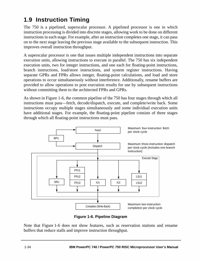
hicherentn pass
n. This
paratedent
ions,aving
stores arections
ch allSomeunitstages
ename
1.9 Instruction TimingThe 750 is a pipelined, superscalar processor. A pipelined processor is one in winstruction processing is divided into discrete stages, allowing work to be done on diffinstructions in each stage. For example, after an instruction completes one stage, it caon to the next stage leaving the previous stage available to the subsequent instructioimproves overall instruction throughput.
A superscalar processor is one that issues multiple independent instructions into seexecution units, allowing instructions to execute in parallel. The 750 has six indepenexecution units, two for integer instructions, and one each for floating-point instructbranch instructions, load/store instructions, and system register instructions. Hseparate GPRs and FPRs allows integer, floating-point calculations, and load andoperations to occur simultaneously without interference. Additionally, rename bufferprovided to allow operations to post execution results for use by subsequent instruwithout committing them to the architected FPRs and GPRs.
As shown in Figure 1-6, the common pipeline of the 750 has four stages through whiinstructions must pass—fetch, decode/dispatch, execute, and complete/write back.instructions occupy multiple stages simultaneously and some individual executionhave additional stages. For example, the floating-point pipeline consists of three sthrough which all floating-point instructions must pass.
Figure 1-6. Pipeline Diagram
Note that Figure 1-6 does not show features, such as reservation stations and rbuffers that reduce stalls and improve instruction throughput.
Fetch
Complete (Write-Back)
Dispatch
Execute Stage
FPU3SRU IU2IU1
Maximum three-instruction dispatchper clock cycle (includes one branchinstruction)
Maximum two-instructioncompletion per clock cycle
FPU2
FPU1
LSU1
Maximum four-instruction fetchper clock cycle
LSU2
BPU
1-34 IBM PowerPC 740 / PowerPC 750 RISC Microprocessor User’s Manual

ws:
orydesr LR
ethe
fromf aname
the
eumtion.
for a
rites
ernaltage is
PUPU
firsttage
and(anding
tomsing
riate
The instruction pipeline in the 750 has four major pipeline stages, described as follo
• The fetch pipeline stage primarily involves retrieving instructions from the memsystem and determining the location of the next instruction fetch. The BPU decobranches during the fetch stage and removes those that do not update CTR ofrom the instruction stream.
• The dispatch stage is responsible for decoding the instructions supplied by thinstruction fetch stage and determining which instructions can be dispatched incurrent cycle. If source operands for the instruction are available, they are readthe appropriate register file or rename register to the execute pipeline stage. Isource operand is not available, dispatch provides a tag that indicates which reregister will supply the operand when it becomes available. At the end of thedispatch stage, the dispatched instructions and their operands are latched byappropriate execution unit.
• Instructions executed by the IUs, FPU, SRU, and LSU are dispatched from thbottom two positions in the instruction queue. In a single clock cycle, a maximof two instructions can be dispatched to these execution units in any combinaWhen an instruction is dispatched, it is assigned a position in the six-entrycompletion queue. A branch instruction can be issued on the same clock cyclemaximum three-instruction dispatch.
• During the execute pipeline stage, each execution unit that has an executableinstruction executes the selected instruction (perhaps over multiple cycles), wthe instruction's result into the appropriate rename register, and notifies thecompletion stage that the instruction has finished execution. In the case of an intexception, the execution unit reports the exception to the completion pipeline sand (except for the FPU) discontinues instruction execution until the exceptionhandled. The exception is not signaled until that instruction is the next to becompleted. Execution of most floating-point instructions is pipelined within the Fallowing up to three instructions to be executing in the FPU concurrently. The Fstages are multiply, add, and round-convert. Execution of most load/storeinstructions is also pipelined. The load/store unit has two pipeline stages. Thestage is for effective address calculation and MMU translation and the second sis for accessing the data in the cache.
• The complete pipeline stage maintains the correct architectural machine statetransfers execution results from the rename registers to the GPRs and FPRs CTR and LR, for some instructions) as instructions are retired. As with dispatchinstructions from the instruction queue, instructions are retired from the two botpositions in the completion queue. If completion logic detects an instruction cauan exception, all following instructions are cancelled, their execution results inrename registers are discarded, and instructions are fetched from the appropexception vector.
Chapter 1. PowerPC 740/PowerPC 750 Overview 1-35

ty of
s for
in the
andtheill
is inupt, ato thetate
full-
ping,turnsstemchinew
LLt, a
aving
Because the PowerPC architecture can be applied to such a wide varieimplementations, instruction timing varies among PowerPC processors.
For a detailed discussion of instruction timing with examples and a table of latencieeach execution unit, see Chapter 6, “Instruction Timing.”
1.10 Power ManagementThe 750 provides four power modes, selectable by setting the appropriate control bitsMSR and HID0 registers. The four power modes are as follows:
• Full-power—This is the default power state of the 750. The 750 is fully poweredthe internal functional units are operating at the full processor clock speed. If dynamic power management mode is enabled, functional units that are idle wautomatically enter a low-power state without affecting performance, softwareexecution, or external hardware.
• Doze—All the functional units of the 750 are disabled except for the timebase/decrementer registers and the bus snooping logic. When the processor doze mode, an external asynchronous interrupt, a system management interrdecrementer exception, a hard or soft reset, or machine check brings the 750 infull-power state. The 750 in doze mode maintains the PLL in a fully powered sand locked to the system external clock input (SYSCLK) so a transition to thepower state takes only a few processor clock cycles.
• Nap—The nap mode further reduces power consumption by disabling bus snooleaving only the time base register and the PLL in a powered state. The 750 reto the full-power state upon receipt of an external asynchronous interrupt, a symanagement interrupt, a decrementer exception, a hard or soft reset, or a macheck input (MCP). A return to full-power state from a nap state takes only a feprocessor clock cycles. When the processor is in nap mode, ifQACK is negated, theprocessor is put in doze mode to support snooping.
• Sleep—Sleep mode minimizes power consumption by disabling all internalfunctional units, after which external system logic may disable the PLL andSYSCLK. Returning the 750 to the full-power state requires the enabling of the Pand SYSCLK, followed by the assertion of an external asynchronous interrupsystem management interrupt, a hard or soft reset, or a machine check input (MCP)signal after the time required to relock the PLL.
Chapter 10, “Power and Thermal Management,” provides information about power sand thermal management modes for the 750.
1-36 IBM PowerPC 740 / PowerPC 750 RISC Microprocessor User’s Manual

ilitysizet sink
high
ratingm canr the
raturefrom
ermal
ntroland
eshold
sas
alholdRM1
leruptll as
e byrough
aving
1.11 Thermal ManagementThe 750’s thermal assist unit (TAU) provides a way to control heat dissipation. This abis particularly useful in portable computers, which, due to power consumption andlimitations, cannot use desktop cooling solutions such as fans. Therefore, better headesigns coupled with intelligent thermal management is of critical importance forperformance portable systems.
Primarily, the thermal management system monitors and regulates the system’s opetemperature. For example, if the temperature is about to exceed a set limit, the systebe made to slow down or even suspend operations temporarily in order to lowetemperature.
The thermal management facility also ensures that the processor’s junction tempedoes not exceed the operating specification. To avoid the inaccuracies that arisemeasuring junction temperature with an external thermal sensor, the 750’s on-chip thsensor and logic tightly couples the thermal management implementation.
The TAU consists of a thermal sensor, digital-to-analog convertor, comparator, cologic, and the dedicated SPRs described in Section 1.4, “PowerPC RegistersProgramming Model.” The TAU does the following:
• Compares the junction temperature against user-programmable thresholds
• Generates a thermal management interrupt if the temperature crosses the thr
• Enables the user to estimate the junction temperature by way of a softwaresuccessive approximation routine
The TAU is controlled through the privilegedmtspr/mfspr instructions to the three SPRprovided for configuring and controlling the sensor control logic, which functionfollows:
• THRM1 and THRM2 provide the ability to compare the junction temperatureagainst two user-provided thresholds. Having dual thresholds gives the thermmanagement software finer control of the junction temperature. In single thresmode, the thermal sensor output is compared to only one threshold in either THor THRM2.
• THRM3 is used to enable the TAU and to control the comparator output samptime. The thermal management logic manages the thermal management intergeneration and time multiplexed comparisons in the dual threshold mode as weother control functions.
Instruction cache throttling provides control of the 750’s overall junction temperaturdetermining the interval at which instructions are fetched. This feature is accessed ththe ICTC register.
Chapter 10, “Power and Thermal Management,” provides information about power sand thermal management modes for the 750.
Chapter 1. PowerPC 740/PowerPC 750 Overview 1-37

o helpountsmory
to byccesserPC0 ors fortionr the
gram
from
nitor
1.12 Performance MonitorThe 750 incorporates a performance monitor facility that system designers can use tbring up, debug, and optimize software performance. The performance monitor cevents during execution of code, relating to dispatch, execution, completion, and meaccesses.
The performance monitor incorporates several registers that can be read and writtensupervisor-level software. User-level versions of these registers provide read-only afor user-level applications. These registers are described in Section 1.4, “PowRegisters and Programming Model.” Performance monitor control registers, MMCRMMCR1, can be used to specify which events are to be counted and the conditionwhich a performance monitoring interrupt is taken. Additionally, the sampled instrucaddress register, SIA (USIA), holds the address of the first instruction to complete aftecounter overflowed.
Attempting to write to a user-read-only performance monitor register causes a proexception, regardless of the MSR[PR] setting.
When a performance monitoring interrupt occurs, program execution continuesvector offset 0x00F00.
Chapter 11, “Performance Monitor,” describes the operation of the performance modiagnostic tool incorporated in the 750.
1-38 IBM PowerPC 740 / PowerPC 750 RISC Microprocessor User’s Manual

atureserPC
ew ofheseisters.ter 2,
on setentfor alln-chipegisterrceg themory
ght ofof thess the
Chapter 2Programming Model2020
This chapter describes the PowerPC 750 programming model, emphasizing those fespecific to the 750 processor and summarizing those that are common to Powprocessors. It consists of three major sections, which describe the following:
• Registers implemented in the 750• Operand conventions• The 750 instruction set
For detailed information about architecture-defined features, seeThe ProgrammingEnvironments Manual.
2.1 The PowerPC 750 Processor Register SetThis section describes the registers implemented in the 750. It includes an overviregisters defined by the PowerPC architecture, highlighting differences in how tregisters are implemented in the 750, and a detailed description of 750-specific regFull descriptions of the architecture-defined register set are provided in Chap“PowerPC Register Set,” inThe Programming Environments Manual.
Registers are defined at all three levels of the PowerPC architecture—user instructiarchitecture (UISA), virtual environment architecture (VEA), and operating environmarchitecture (OEA). The PowerPC architecture defines register-to-register operationscomputational instructions. Source data for these instructions are accessed from the oregisters or are provided as immediate values embedded in the opcode. The three-rinstruction format allows specification of a target register distinct from the two souregisters, thus preserving the original data for use by other instructions and reducinnumber of instructions required for certain operations. Data is transferred between meand registers with explicit load and store instructions only.
2.1.1 Register SetThe registers implemented on the 750 are shown in Figure 2-1. The number to the rithe special-purpose registers (SPRs) indicates the number that is used in the syntaxinstruction operands to access the register (for example, the number used to acce
Chapter 2. Programming Model 2-1
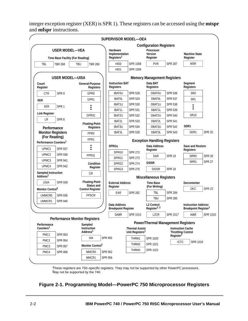
integer exception register (XER) is SPR 1). These registers can be accessed using themtsprandmfspr instructions.
Figure 2-1. Programming Model—PowerPC 750 Microprocessor Registers
ICTC SPR 1019SPR 1020
SPR 1021
SPR 1022
THRM1
THRM2
THRM3
SPR 937
SPR 938
SPR 941
SPR 942
PerformanceCounters 1
SampledInstructionAddress 1
DSISR
Data AddressRegister
SPRGs
Exception Handling RegistersSave and RestoreRegisters
Instruction BATRegisters
Data BATRegisters
Memory Management Registers
Machine StateRegister
MSR
ProcessorVersionRegister
SPR 287PVR
Configuration RegistersHardwareImplementationRegisters 1
SPR 1
USER MODEL—UISA
Floating-PointStatus and
Control Register
FPSCR
ConditionRegister
General-PurposeRegisters
XER
XER
SPR 8
Link Register
LR
SUPERVISOR MODEL—OEA
DecrementerExternal AddressRegister
EAR
SDR1
SPR 9
CountRegister
Miscellaneous Registers
SegmentRegisters
1These registers are 750–specific registers. They may not be supported by other PowerPC processors.
CR
Floating-PointRegistersPerformance
Monitor Registers(For Reading)
Performance Counters 1
Monitor Control 1
SPR 939USIA
Sampled InstructionAddress 1
Performance Monitor Registers
Monitor Control 1
Time Base(For Writing)
Power/Thermal Management RegistersThermal AssistUnit Registers 1
Instruction CacheThrottling ControlRegister 1
USER MODEL—VEA
TBL TBR 268
Time Base Facility (For Reading)
CTR
2May not be supported by the 740.
GPR0
GPR1
GPR31
TBU TBR 269
IBAT0U
IBAT0L
IBAT1U
IBAT1L
IBAT2U
IBAT2L
IBAT3U
IBAT3L
SPR 528
SPR 529
SPR 530
SPR 531
SPR 532
SPR 533
SPR 534
SPR 535
SPR 536
SPR 537
SPR 538
SPR 539
SPR 540
SPR 541
SPR 542
SPR 543
DBAT0U
DBAT0L
DBAT1U
DBAT1L
DBAT2U
DBAT2L
DBAT3U
DBAT3L
SR0
SR1
SR15
SDR1 SPR 25
HID0
HID1
SPR 1008
SPR 1009
FPR0
FPR1
FPR31
UPMC1
UPMC2
UPMC3
UPMC4
UMMCR0
UMMCR1
SPR 936
SPR 940
SPR 953
SPR 954
SPR 957
SPR 958
PMC1
PMC2
PMC3
PMC4
SIA SPR 955
MMCR0
MMCR1
SPR 952
SPR 956
SPRG0
SPRG1
SPRG2
SPRG3
SPR 272
SPR 273
SPR 274
SPR 275
DAR
DSISR
SPR 19
SPR 18
SRR0 SPR 26
SRR1 SPR 27
SPR 282 TBL SPR 284
TBU SPR 285
DEC SPR 22
Data AddressBreakpoint Register
DABR SPR 1013
L2 ControlRegister 1, 2
L2CR SPR 1017
Instruction AddressBreakpoint Register 1
IABR SPR 1010
2-2 IBM PowerPC 740 / PowerPC 750 RISC Microprocessor User’s Manual

) andss to
e to
are
PRrPC’s
servedatater 2,
as
7,for
rPC
llble
l
ture
int of
orster
ead
ch
The PowerPC UISA registers are user-level. General-purpose registers (GPRsfloating-point registers (FPRs) are accessed through instruction operands. Acceregisters can be explicit (by using instructions for that purpose such as MovSpecial-Purpose Register (mtspr) and Move from Special-Purpose Register (mfspr)instructions) or implicit as part of the execution of an instruction. Some registersaccessed both explicitly and implicitly.
Implementation Note—The 750 fully decodes the SPR field of the instruction. If the Sspecified is undefined, the illegal instruction program exception occurs. The Poweuser-level registers are described as follows:
• User-level registers (UISA)—The user-level registers can be accessed by allsoftware with either user or supervisor privileges. They include the following:
— General-purpose registers (GPRs). The thirty-two GPRs (GPR0–GPR31) as data source or destination registers for integer instructions and provide for generating addresses. See “General Purpose Registers (GPRs),” in Chap“PowerPC Register Set,” ofThe Programming Environments Manualfor moreinformation.
— Floating-point registers (FPRs). The thirty-two FPRs (FPR0–FPR31) servethe data source or destination for all floating-point instructions. See“Floating-Point Registers (FPRs),” in Chapter 2, “PowerPC Register Set,” ofTheProgramming Environments Manual.
— Condition register (CR). The 32-bit CR consists of eight 4-bit fields, CR0–CRthat reflect results of certain arithmetic operations and provide a mechanismtesting and branching. See “Condition Register (CR),” in Chapter 2, “PoweRegister Set,” ofThe Programming Environments Manual.
— Floating-point status and control register (FPSCR). The FPSCR contains afloating-point exception signal bits, exception summary bits, exception enabits, and rounding control bits needed for compliance with the IEEE 754standard. See “Floating-Point Status and Control Register (FPSCR),” inChapter 2, “PowerPC Register Set,” ofThe Programming Environments Manua.
The remaining user-level registers are SPRs. Note that the PowerPC architecprovides a separate mechanism for accessing SPRs (themtspr andmfsprinstructions). These instructions are commonly used to explicitly access certaregisters, while other SPRs may be more typically accessed as the side effecexecuting other instructions.
— Integer exception register (XER). The XER indicates overflow and carries finteger operations. See “XER Register (XER),” in Chapter 2, “PowerPC RegiSet,” ofThe Programming Environments Manualfor more information.
Implementation Note—To allow emulation of thelscbx instruction defined bythe POWER architecture, XER[16–23] is implemented so that they can be rwith mfspr[XER] and written withmtxer[XER] instructions.
— Link register (LR). The LR provides the branch target address for the Bran
Chapter 2. Programming Model 2-3

2,
dalsoister
aselore
other
sor.
tatustate
s
Conditional to Link Register (bclrx) instruction, and can be used to hold thelogical address of the instruction that follows a branch and link instruction,typically used for linking to subroutines. See “Link Register (LR),” in Chapter“PowerPC Register Set,” ofThe Programming Environments Manual.
— Count register (CTR). The CTR holds a loop count that can be decrementeduring execution of appropriately coded branch instructions. The CTR canprovide the branch target address for the Branch Conditional to Count Reg(bcctrx) instruction. See “Count Register (CTR),” in Chapter 2, “PowerPCRegister Set,” ofThe Programming Environments Manual.
• User-level registers (VEA)—The PowerPC VEA defines the time base facility(TB), which consists of two 32-bit registers—time base upper (TBU) and time blower (TBL). The time base registers can be written to only by supervisor-leveinstructions but can be read by both user- and supervisor-level software. For minformation, see “PowerPC VEA Register Set—Time Base,” in Chapter 2,“PowerPC Register Set,” ofThe Programming Environments Manual.
• Supervisor-level registers(OEA)—The OEA defines the registers an operatingsystem uses for memory management, configuration, exception handling, andoperating system functions. The OEA defines the following supervisor-levelregisters for 32-bit implementations:
— Configuration registers
– Machine state register (MSR). The MSR defines the state of the procesThe MSR can be modified by the Move to Machine State Register (mtmsr),System Call (sc), and Return from Exception (rfi ) instructions. It can be readby the Move from Machine State Register (mfmsr) instruction. When anexception is taken, the contents of the MSR are saved to the machine ssave/restore register 1 (SRR1), which is described below. See “Machine SRegister (MSR),” in Chapter 2, “PowerPC Register Set,” ofThe ProgrammingEnvironments Manualfor more information.
Implementation Note—Table 2-1 describes MSR bits the 750 implementthat are not required by the PowerPC architecture.
Table 2-1. Additional MSR Bits
Bit Name Description
13 POW Power management enable. Optional to the PowerPC architecture.0 Power management is disabled.1 Power management is enabled. The processor can enter a power-saving mode when additional
conditions are present. The mode chosen is determined by the DOZE, NAP, and SLEEP bits inthe hardware implementation-dependent register 0 (HID0), described in Table 2-4.
29 PM Performance monitor marked mode. This bit is specific to the 750, and is defined as reserved bythe PowerPC architecture. See Chapter 11, “Performance Monitor.”0 Process is not a marked process.1 Process is a marked process.
2-4 IBM PowerPC 740 / PowerPC 750 RISC Microprocessor User’s Manual

rnal
ns.
ator.r 2,
for
anourters
s.ter
tions
tois
nPC
ent
Us)theled
Note that setting MSR[EE] masks not only the architecture-defined exteinterrupt and decrementer exceptions but also the 750-specific systemmanagement, performance monitor, and thermal management exceptio
– Processor version register (PVR). This register is a read-only register thidentifies the version (model) and revision level of the PowerPC processFor more information, see “Processor Version Register (PVR),” in Chapte“PowerPC Register Set,” ofThe Programming Environments Manual.
Implementation Note—The processor version information is listed in thePowerPC 740 and PowerPC 750 Embedded Microprocessor: HardwareSpecifications.The processor revision level starts at 0x0100 and is updatedeach silicon revision.
— Memory management registers
– Block-address translation (BAT) registers. The PowerPC OEA includes array of block address translation registers that can be used to specify fblocks of instruction space and four blocks of data space. The BAT regisare implemented in pairs—four pairs of instruction BATs (IBAT0U–IBAT3Uand IBAT0L–IBAT3L) and four pairs of data BATs (DBAT0U–DBAT3U andDBAT0L–DBAT3L). Figure 2-1 lists the SPR numbers for the BAT registerFor more information, see “BAT Registers,” in Chapter 2, “PowerPC RegisSet,” ofThe Programming Environments Manual. Because BAT upper andlower words are loaded separately, software must ensure that BAT translaare correct during the time that both BAT entries are being loaded.
The 750 implements the G bit in the IBAT registers; however, attemptingexecute code from an IBAT area with G = 1 causes an ISI exception. Thcomplies with the revision of the architecture described inThe ProgrammingEnvironments Manual.
– SDR1. The SDR1 register specifies the page table base address used ivirtual-to-physical address translation. See “SDR1,” in Chapter 2, “PowerRegister Set,” ofThe Programming Environments Manual.”
– Segment registers (SR). The PowerPC OEA defines sixteen 32-bit segmregisters (SR0–SR15). Note that the SRs are implemented on 32-bitimplementations only. The fields in the segment register are interpreteddifferently depending on the value of bit 0. See “Segment Registers,” inChapter 2, “PowerPC Register Set,” ofThe Programming EnvironmentsManual for more information.
Note that the 750 implements separate memory management units (MMfor instruction and data. It associates the architecture-defined SRs with data MMU (DMMU). It reflects the values of the SRs in separate, so-cal‘shadow’ segment registers in the instruction MMU (IMMU).
Chapter 2. Programming Model 2-5

iseef
tingt,” of
ed to
us,” of
ed to
0750
e
aseread
— Exception-handling registers
– Data address register (DAR). After a DSI or an alignment exception, DARset to the effective address (EA) generated by the faulting instruction. S“Data Address Register (DAR),” in Chapter 2, “PowerPC Register Set,” oThe Programming Environments Manualfor more information.
– SPRG0–SPRG3. The SPRG0–SPRG3 registers are provided for operasystem use. See “SPRG0–SPRG3,” in Chapter 2, “PowerPC Register SeThe Programming Environments Manualfor more information.
– DSISR. The DSISR register defines the cause of DSI and alignmentexceptions. See “DSISR,” in Chapter 2, “PowerPC Register Set,” ofTheProgramming Environments Manualfor more information.
– Machine status save/restore register 0 (SRR0). The SRR0 register is ussave the address of the instruction at which execution continues whenrfiexecutes at the end of an exception handler routine. See “Machine StatSave/Restore Register 0 (SRR0),” in Chapter 2, “PowerPC Register SetThe Programming Environments Manual for more information.
– Machine status save/restore register 1 (SRR1). The SRR1 register is ussave machine status on exceptions and to restore machine status whenrfiexecutes. See “Machine Status Save/Restore Register 1 (SRR1),” inChapter 2, “PowerPC Register Set,” ofThe Programming EnvironmentsManual for more information.
Implementation Note—When a machine check exception occurs, the 75sets one or more error bits in SRR1. Table 2-2 describes SRR1 bits the implements that are not required by the PowerPC architecture.
— Miscellaneous registers
– Time base (TB). The TB is a 64-bit structure provided for maintaining thtime of day and operating interval timers. The TB consists of two 32-bitregisters—time base upper (TBU) and time base lower (TBL). The time bregisters can be written to only by supervisor-level software, but can be by both user- and supervisor-level software. See “Time Base Facility(TB)—OEA,” in Chapter 2, “PowerPC Register Set,” ofThe Programming
Table 2-2. Additional SRR1 Bits
Bit Name Description
11 L2DP Set by a data parity error on the L2 bus. The PowerPC 740 does not implement the L2 cacheinterface.
12 MCPIN Set by the assertion of MCP
13 TEA Set by a TEA assertion on the 60x bus
14 DP Set by a data parity error on the 60x bus
15 AP Set by an address parity error on the 60x bus
2-6 IBM PowerPC 740 / PowerPC 750 RISC Microprocessor User’s Manual
ter
ck.,” of
ed
to. See
tion
rnal
at in
tored.
rolsling,
cts
L2ssor
nd
cordvide
ble
Environments Manualfor more information.
– Decrementer register (DEC). This register is a 32-bit decrementing counthat provides a mechanism for causing a decrementer exception after aprogrammable delay; the frequency is a subdivision of the processor cloSee “Decrementer Register (DEC),” in Chapter 2, “PowerPC Register SetThe Programming Environments Manualfor more information.
Implementation Note—In the 750, the decrementer register is decrementat a speed that is one-fourth the speed of the bus clock.
– Data address breakpoint register (DABR)—This optional register is usedcause a breakpoint exception if a specified data address is encountered“Data Address Breakpoint Register (DABR),” in Chapter 2, “PowerPCRegister Set,” ofThe Programming Environments Manual.”
– External access register (EAR). This optional register is used in conjuncwith eciwx andecowx. Note that the EAR register and theeciwx andecowxinstructions are optional in the PowerPC architecture and may not besupported in all PowerPC processors that implement the OEA. See “ExteAccess Register (EAR),” in Chapter 2, “PowerPC Register Set,” ofTheProgramming Environments Manual for more information.
• 750-specific registers—The PowerPC architecture allows implementation-specific SPRs. Those incorporated in the 750 are described as follows. Note ththe 750, these registers are all supervisor-level registers.
— Instruction address breakpoint register (IABR)—This register can be used cause a breakpoint exception if a specified instruction address is encounte
— Hardware implementation-dependent register 0 (HID0)—This register contvarious functions, such as enabling checkstop conditions, and locking, enaband invalidating the instruction and data caches.
— Hardware implementation-dependent register 1 (HID1)—This register reflethe state of PLL_CFG[0–3] clock signals.
— The L2 cache control register (L2CR) is used to configure and operate thecache. It includes bits for enabling parity checking, setting the L2-to-proceclock ratio, and identifying the type of RAM used for the L2 cacheimplementation. (Not supported in the 740.)
— Performance monitor registers. The following registers are used to define acount events for use by the performance monitor:
– The performance monitor counter registers (PMC1–PMC4) are used to rethe number of times a certain event has occurred. UPMC1–UPMC4 prouser-level read access to these registers.
– The monitor mode control registers (MMCR0–MMCR1) are used to enavarious performance monitor interrupt functions. UMMCR0–UMMCR1provide user-level read access to these registers.
Chapter 2. Programming Model 2-7

resss the
r the
ut
the
rermalninther
d to
rs isilar or
in the
ctionresses
thegersn, seen be
– The sampled instruction address register (SIA) contains the effective addof an instruction executing at or around the time that the processor signalperformance monitor interrupt condition. USIA provides user-level readaccess to the SIA.
– The 750 does not implement the sampled data address register (SDA) ouser-level, read-only USDA registers. However, for compatibility withprocessors that do, those registers can be written to by boot code withocausing an exception. SDA is SPR 959; USDA is SPR 943.
— The instruction cache throttling control register (ICTC) has bits for enablinginstruction cache throttling feature and for controlling the interval at whichinstructions are forwarded to the instruction buffer in the fetch unit. Thisprovides control over the processor’s overall junction temperature.
— Thermal management registers (THRM1, THRM2, and THRM3). Used toenable and set thresholds for the thermal management facility.
– THRM1 and THRM2 provide the ability to compare the junction temperatuagainst two user-provided thresholds. The dual thresholds allow the themanagement software differing degrees of action in lowering the junctiotemperature. The TAU can be also operated in a single threshold mode which the thermal sensor output is compared to only one threshold in eiTHRM1 or THRM2.
– THRM3 is used to enable the thermal management assist unit (TAU) ancontrol the comparator output sample time.
Note that while it is not guaranteed that the implementation of 750-specific registeconsistent among PowerPC processors, other processors may implement simidentical registers.
2.1.2 PowerPC 750-Specific RegistersThis section describes registers that are defined for the 750 but are not includedPowerPC architecture.
2.1.2.1 Instruction Address Breakpoint Register (IABR)The address breakpoint register (IABR), shown in Figure 2-2, supports the instruaddress breakpoint exception. When this exception is enabled, instruction fetch addare compared with an effective address stored in the IABR. If the word specified inIABR is fetched, the instruction breakpoint handler is invoked. The instruction that trigthe breakpoint does not execute before the handler is invoked. For more informatioSection 4.5.14, “Instruction Address Breakpoint Exception (0x01300).” The IABR caaccessed withmtspr andmfspr using the SPR1010.
2-8 IBM PowerPC 740 / PowerPC 750 RISC Microprocessor User’s Manual

veral
Figure 2-2. Instruction Address Breakpoint Register
The IABR bits are described in Table 2-3.
2.1.2.2 Hardware Implementation-Dependent Register 0The hardware implementation-dependent register 0 (HID0) controls the state of sefunctions within the 750. The HID0 register is shown in Figure 2-3.
Figure 2-3 . Hardware Implementation-Dependent Register 0 (HID0)
The HID0 bits are described in Table 2-4.
Table 2-3. Instruction Address Breakpoint Register Bit Settings
Bits Name Description
0–29 Address Word address to be compared
30 BE Breakpoint enabled. Setting this bit indicates that breakpoint checking is to be done.
31 TE Translation enabled. An IABR match is signaled if this bit matches MSR[IR].
Table 2-4. HID0 Bit Functions
Bit Name Function
0 EMCP Enable MCP. The primary purpose of this bit is to mask out further machine check exceptionscaused by assertion of MCP, similar to how MSR[EE] can mask external interrupts.0 Masks MCP. Asserting MCP does not generate a machine check exception or a checkstop.1 Asserting MCP causes checkstop if MSR[ME] = 0 or a machine check exception if ME = 1.
1 DBP Enable/disable 60x bus address and data parity generation.0 Parity generation is enabled.1 If the system does not use address or data parity and the respective parity checking is disabled
(HID0[EBA] or HID0[EBD] = 0), input receivers for those signals are disabled, require no pull-upresistors, and thus should be left unconnected. If all parity generation is disabled, all paritychecking should also be disabled and parity signals need not be connected.
2 EBA Enable/disable 60x bus address parity checking0 Prevents address parity checking.1 Allows a address parity error to cause a checkstop if MSR[ME] = 0 or a machine check
exception if MSR[ME] = 1.EBA and EBD allow the processor to operate with memory subsystems that do not generate parity.
0 29 30 31
Address BE TE
EBDEBA PAR NAP DPM NHR ICE DCE DCFI
EMCP BCLK ECLK DOZE SLEEP ILOCKDLOCK
ICFI SPD DCFA BTIC
0 1 2 3 4 5 6 7 8 9 10 11 12 13 14 15 16 17 18 19 20 21 22 23 24 25 26 27 28 29 30 31
Reserved
BHTABE00DBP 00 0IFEM SGE
NOOPTI
0
Chapter 2. Programming Model 2-9

3 EBD Enable 60x bus data parity checking0 Parity checking is disabled.1 Allows a data parity error to cause a checkstop if MSR[ME] = 0 or a machine check exception if
MSR[ME] = 1.EBA and EBD allow the processor to operate with memory subsystems that do not generate parity.
4 BCLK CLK_OUT output enable and clock type selection. Used in conjunction with HID0[ECLK] and theHRESET signal to configure CLK_OUT. See Table 2-5.
5 — Not used. Defined as EICE on some earlier processors.
6 ECLK CLK_OUT output enable and clock type selection. Used in conjunction with HID0[BCLK] and theHRESET signal to configure CLK_OUT. See Table 2-5.
7 PAR Disable precharge of ARTRY.0 Precharge of ARTRY enabled1 Alters bus protocol slightly by preventing the processor from driving ARTRY to high (negated)
state. If this is done, the system must restore the signals to the high state.
8 DOZE Doze mode enable. Operates in conjunction with MSR[POW].0 Doze mode disabled.1 Doze mode enabled. Doze mode is invoked by setting MSR[POW] while this bit is set. In doze
mode, the PLL, time base, and snooping remain active.
9 NAP Nap mode enable. Operates in conjunction with MSR[POW].0 Nap mode disabled.1 Nap mode enabled. Doze mode is invoked by setting MSR[POW] while this bit is set. In nap
mode, the PLL and the time base remain active.
10 SLEEP Sleep mode enable. Operates in conjunction with MSR[POW].0 Sleep mode disabled.1 Sleep mode enabled. Sleep mode is invoked by setting MSR[POW] while this bit is set. QREQ is
asserted to indicate that the processor is ready to enter sleep mode. If the system logicdetermines that the processor may enter sleep mode, the quiesce acknowledge signal, QACK,is asserted back to the processor. Once QACK assertion is detected, the processor enterssleep mode after several processor clocks. At this point, the system logic may turn off the PLLby first configuring PLL_CFG[0–3] to PLL bypass mode, then disabling SYSCLK.
11 DPM Dynamic power management enable.0 Dynamic power management is disabled.1 Functional units enter a low-power mode automatically if the unit is idle. This does not affect
operational performance and is transparent to software or any external hardware.
12–14 — Not used
15 NHR Not hard reset (software-use only)—Helps software distinguish a hard reset from a soft reset.0 A hard reset occurred if software had previously set this bit.1 A hard reset has not occurred. If software sets this bit after a hard reset, when a reset occurs
and this bit remains set, software can tell it was a soft reset.
16 ICE Instruction cache enable0 The instruction cache is neither accessed nor updated. All pages are accessed as if they were
marked cache-inhibited (WIM = X1X). Potential cache accesses from the bus (snoop and cacheoperations) are ignored. In the disabled state for the L1 caches, the cache tag state bits areignored and all accesses are propagated to the L2 cache or bus as single-beat transactions. Forthose transactions, however, CI reflects the original state determined by address translationregardless of cache disabled status. ICE is zero at power-up.
1 The instruction cache is enabled
Table 2-4. HID0 Bit Functions (Continued)
Bit Name Function
2-10 IBM PowerPC 740 / PowerPC 750 RISC Microprocessor User’s Manual
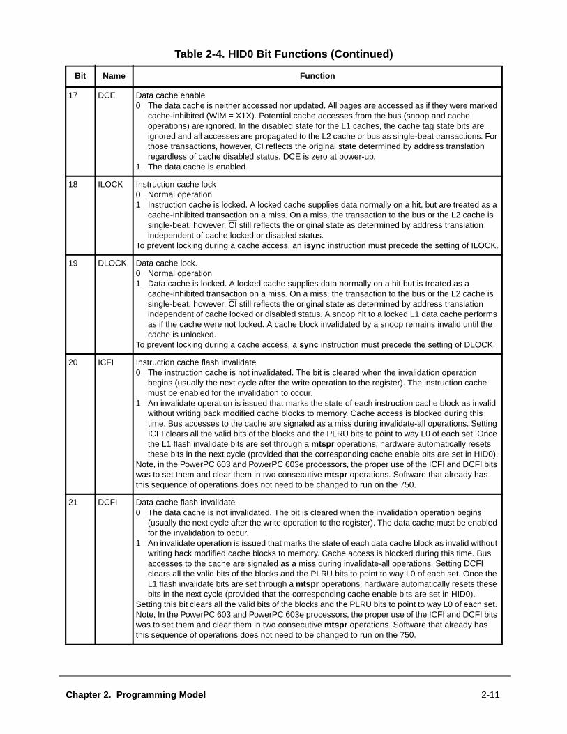
17 DCE Data cache enable0 The data cache is neither accessed nor updated. All pages are accessed as if they were marked
cache-inhibited (WIM = X1X). Potential cache accesses from the bus (snoop and cacheoperations) are ignored. In the disabled state for the L1 caches, the cache tag state bits areignored and all accesses are propagated to the L2 cache or bus as single-beat transactions. Forthose transactions, however, CI reflects the original state determined by address translationregardless of cache disabled status. DCE is zero at power-up.
1 The data cache is enabled.
18 ILOCK Instruction cache lock0 Normal operation1 Instruction cache is locked. A locked cache supplies data normally on a hit, but are treated as a
cache-inhibited transaction on a miss. On a miss, the transaction to the bus or the L2 cache issingle-beat, however, CI still reflects the original state as determined by address translationindependent of cache locked or disabled status.
To prevent locking during a cache access, an isync instruction must precede the setting of ILOCK.
19 DLOCK Data cache lock.0 Normal operation1 Data cache is locked. A locked cache supplies data normally on a hit but is treated as a
cache-inhibited transaction on a miss. On a miss, the transaction to the bus or the L2 cache issingle-beat, however, CI still reflects the original state as determined by address translationindependent of cache locked or disabled status. A snoop hit to a locked L1 data cache performsas if the cache were not locked. A cache block invalidated by a snoop remains invalid until thecache is unlocked.
To prevent locking during a cache access, a sync instruction must precede the setting of DLOCK.
20 ICFI Instruction cache flash invalidate0 The instruction cache is not invalidated. The bit is cleared when the invalidation operation
begins (usually the next cycle after the write operation to the register). The instruction cachemust be enabled for the invalidation to occur.
1 An invalidate operation is issued that marks the state of each instruction cache block as invalidwithout writing back modified cache blocks to memory. Cache access is blocked during thistime. Bus accesses to the cache are signaled as a miss during invalidate-all operations. SettingICFI clears all the valid bits of the blocks and the PLRU bits to point to way L0 of each set. Oncethe L1 flash invalidate bits are set through a mtspr operations, hardware automatically resetsthese bits in the next cycle (provided that the corresponding cache enable bits are set in HID0).
Note, in the PowerPC 603 and PowerPC 603e processors, the proper use of the ICFI and DCFI bitswas to set them and clear them in two consecutive mtspr operations. Software that already hasthis sequence of operations does not need to be changed to run on the 750.
21 DCFI Data cache flash invalidate0 The data cache is not invalidated. The bit is cleared when the invalidation operation begins
(usually the next cycle after the write operation to the register). The data cache must be enabledfor the invalidation to occur.
1 An invalidate operation is issued that marks the state of each data cache block as invalid withoutwriting back modified cache blocks to memory. Cache access is blocked during this time. Busaccesses to the cache are signaled as a miss during invalidate-all operations. Setting DCFIclears all the valid bits of the blocks and the PLRU bits to point to way L0 of each set. Once theL1 flash invalidate bits are set through a mtspr operations, hardware automatically resets thesebits in the next cycle (provided that the corresponding cache enable bits are set in HID0).
Setting this bit clears all the valid bits of the blocks and the PLRU bits to point to way L0 of each set.Note, In the PowerPC 603 and PowerPC 603e processors, the proper use of the ICFI and DCFI bitswas to set them and clear them in two consecutive mtspr operations. Software that already hasthis sequence of operations does not need to be changed to run on the 750.
Table 2-4. HID0 Bit Functions (Continued)
Bit Name Function
Chapter 2. Programming Model 2-11

22 SPD Speculative cache access disable0 Speculative bus accesses to nonguarded space (G = 0) from both the instruction and data
caches is enabled1 Speculative bus accesses to nonguarded space in both caches is disabled
23 IFEM Enable M bit on bus for instruction fetches.0 M bit disabled. Instruction fetches are treated as nonglobal on the bus1 Instruction fetches reflect the M bit from the WIM settings.
24 SGE Store gathering enable0 Store gathering is disabled1 Integer store gathering is performed for write-through to nonguarded space or for
cache-inhibited stores to nonguarded space for 4-byte, word-aligned stores. The LSU combinesstores to form a double word that is sent out on the 60x bus as a single-beat operation. Storesare gathered only if successive, eligible stores, are queued and pending. Store gathering isperformed regardless of address order or endian mode.
25 DCFA Data cache flush assist. (Force data cache to ignore invalid sets on miss replacement selection.)0 The data cache flush assist facility is disabled1 The miss replacement algorithm ignores invalid entries and follows the replacement sequence
defined by the PLRU bits. This reduces the series of uniquely addressed load or dcbzinstructions to eight per set. The bit should be set just before beginning a cache flush routineand should be cleared when the series of instructions is complete.
26 BTIC Branch Target Instruction Cache enable—used to enable use of the 64-entry branch instructioncache.0 The BTIC is disabled, the contents are invalidated, and the BTIC behaves as if it was empty.
New entries cannot be added until the BTIC is enabled.1 The BTIC is enabled, and new entries can be added.
27 — Not used. Defined as FBIOB on earlier 603-type processors.
28 ABE Address broadcast enable—controls whether certain address-only operations (such as cacheoperations, eieio , and sync ) are broadcast on the 60x bus.0 Address-only operations affect only local L1 and L2 caches and are not broadcast.1 Address-only operations are broadcast on the 60x bus.Affected instructions are eieio , sync ,
dcbi , dcbf , and dcbst . A sync instruction completes only after a successful broadcast.Execution of eieio causes a broadcast that may be used to prevent any external devices, suchas a bus bridge chip, from store gathering.
Note that dcbz (with M = 1, coherency required) always broadcasts on the 60x bus regardless ofthe setting of this bit. An icbi is never broadcast. No cache operations, except dcbz , are snoopedby the 750 regardless of whether the ABE is set. Bus activity caused by these instructions resultsdirectly from performing the operation on the 750 cache.
29 BHT Branch history table enable0 BHT disabled. The 750 uses static branch prediction as defined by the PowerPC architecture
(UISA) for those branch instructions the BHT would have otherwise used to predict (that is,those that use the CR as the only mechanism to determine direction). For more information onstatic branch prediction, see “Conditional Branch Control,” in Chapter 4 of The ProgrammingEnvironments Manual.
1 Allows the use of the 512-entry branch history table (BHT).The BHT is disabled at power-on reset. All entries are set to weakly, not-taken.
30 — Not used
31 NOOPTI No-op the data cache touch instructions.0 The dcbt and dcbtst instructions are enabled.1 The dcbt and dcbtst instructions are no-oped globally.
Table 2-4. HID0 Bit Functions (Continued)
Bit Name Function
2-12 IBM PowerPC 740 / PowerPC 750 RISC Microprocessor User’s Manual
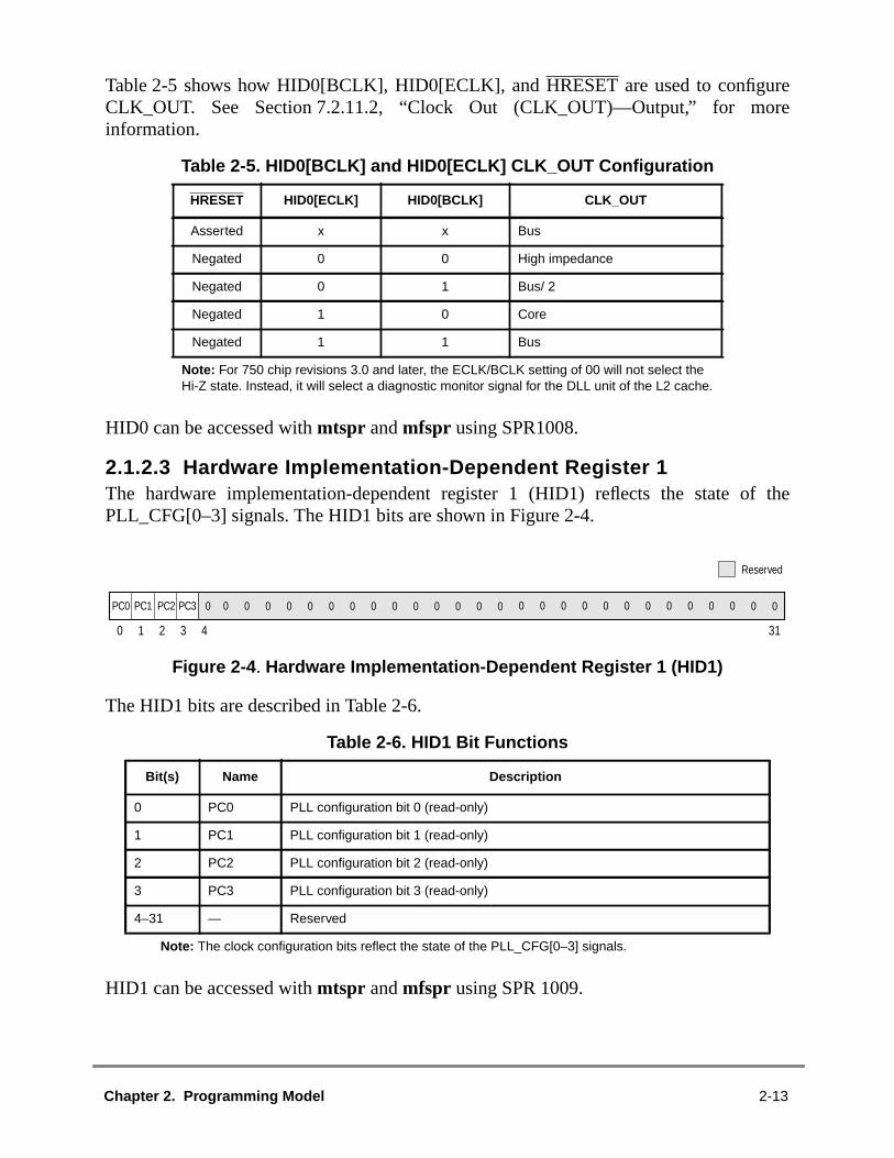
re
f the
Table 2-5 shows how HID0[BCLK], HID0[ECLK], andHRESET are used to configureCLK_OUT. See Section 7.2.11.2, “Clock Out (CLK_OUT)—Output,” for moinformation.
HID0 can be accessed withmtspr andmfspr using SPR1008.
2.1.2.3 Hardware Implementation-Dependent Register 1The hardware implementation-dependent register 1 (HID1) reflects the state oPLL_CFG[0–3] signals. The HID1 bits are shown in Figure 2-4.
Figure 2-4 . Hardware Implementation-Dependent Register 1 (HID1)
The HID1 bits are described in Table 2-6.
HID1 can be accessed withmtspr andmfspr using SPR 1009.
Table 2-5. HID0[BCLK] and HID0[ECLK] CLK_OUT Configuration
HRESET HID0[ECLK] HID0[BCLK] CLK_OUT
Asserted x x Bus
Negated 0 0 High impedance
Negated 0 1 Bus/ 2
Negated 1 0 Core
Negated 1 1 Bus
Note: For 750 chip revisions 3.0 and later, the ECLK/BCLK setting of 00 will not select theHi-Z state. Instead, it will select a diagnostic monitor signal for the DLL unit of the L2 cache.
Table 2-6. HID1 Bit Functions
Bit(s) Name Description
0 PC0 PLL configuration bit 0 (read-only)
1 PC1 PLL configuration bit 1 (read-only)
2 PC2 PLL configuration bit 2 (read-only)
3 PC3 PLL configuration bit 3 (read-only)
4–31 — Reserved
Note: The clock configuration bits reflect the state of the PLL_CFG[0–3] signals.
PC2PC0
0 1 2 3 4 31
PC1
Reserved
PC3 00 00000000000000000000000000
Chapter 2. Programming Model 2-13
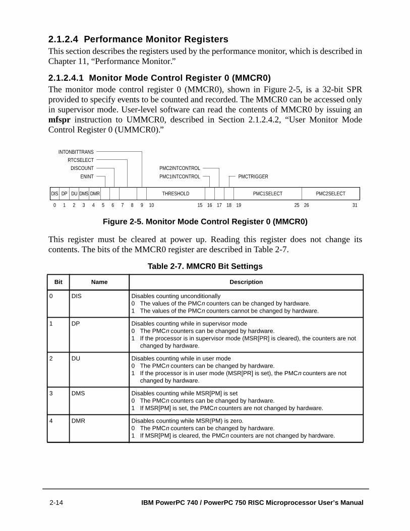
ibed in
PRd onlyg ande
ge its
2.1.2.4 Performance Monitor RegistersThis section describes the registers used by the performance monitor, which is descrChapter 11, “Performance Monitor.”
2.1.2.4.1 Monitor Mode Control Register 0 (MMCR0)The monitor mode control register 0 (MMCR0), shown in Figure 2-5, is a 32-bit Sprovided to specify events to be counted and recorded. The MMCR0 can be accessein supervisor mode. User-level software can read the contents of MMCR0 by issuinmfspr instruction to UMMCR0, described in Section 2.1.2.4.2, “User Monitor MoControl Register 0 (UMMCR0).”
Figure 2-5. Monitor Mode Control Register 0 (MMCR0)
This register must be cleared at power up. Reading this register does not chancontents. The bits of the MMCR0 register are described in Table 2-7.
Table 2-7. MMCR0 Bit Settings
Bit Name Description
0 DIS Disables counting unconditionally0 The values of the PMCn counters can be changed by hardware.1 The values of the PMCn counters cannot be changed by hardware.
1 DP Disables counting while in supervisor mode0 The PMCn counters can be changed by hardware.1 If the processor is in supervisor mode (MSR[PR] is cleared), the counters are not
changed by hardware.
2 DU Disables counting while in user mode0 The PMCn counters can be changed by hardware.1 If the processor is in user mode (MSR[PR] is set), the PMCn counters are not
changed by hardware.
3 DMS Disables counting while MSR[PM] is set0 The PMCn counters can be changed by hardware.1 If MSR[PM] is set, the PMCn counters are not changed by hardware.
4 DMR Disables counting while MSR(PM) is zero.0 The PMCn counters can be changed by hardware.1 If MSR[PM] is cleared, the PMCn counters are not changed by hardware.
INTONBITTRANS
DISCOUNT
PMC1INTCONTROLENINT
PMC2INTCONTROL
RTCSELECT
PMCTRIGGER
DMSDU PMC1SELECT PMC2SELECT
0 1 2 3 4 5 6 7 8 9 10 15 16 17 18 19 25 26 31
DPDIS DMR THRESHOLD
2-14 IBM PowerPC 740 / PowerPC 750 RISC Microprocessor User’s Manual

evel
MMCR0 can be accessed withmtspr andmfspr using SPR 952.
2.1.2.4.2 User Monitor Mode Control Register 0 (UMMCR0)The contents of MMCR0 are reflected to UMMCR0, which can be read by user-lsoftware. MMCR0 can be accessed withmfspr using SPR 936.
5 ENINT Enables performance monitor interrupt signaling.0 Interrupt signaling is disabled.1 Interrupt signaling is enabled.Cleared by hardware when a performance monitor interrupt is signaled. To reenablethese interrupt signals, software must set this bit after handling the performancemonitor interrupt. The IPL ROM code clears this bit before passing control to theoperating system.
6 DISCOUNT Disables counting of PMCn when a performance monitor interrupt is signaled (that is,((PMCnINTCONTROL = 1) & (PMCn[0] = 1) & (ENINT = 1)) or the occurrence of anenabled time base transition with ((INTONBITTRANS =1) & (ENINT = 1)).0 Signaling a performance monitor interrupt does not affect counting status of PMCn.1 The signaling of a performance monitor interrupt prevents changing of PMC1
counter. The PMCn counter do not change if PMC2COUNTCTL = 0.Because a time base signal could have occurred along with an enabled counteroverflow condition, software should always reset INTONBITTRANS to zero, if the valuein INTONBITTRANS was a one.
7–8 RTCSELECT 64-bit time base, bit selection enable00 Pick bit 63 to count01 Pick bit 55 to count10 Pick bit 51 to count11 Pick bit 47 to count
9 INTONBITTRANS Cause interrupt signaling on bit transition (identified in RTCSELECT) from off to on0 Do not allow interrupt signal if chosen bit transitions.1 Signal interrupt if chosen bit transitions.Software is responsible for setting and clearing INTONBITTRANS.
10–15 THRESHOLD Threshold value. The 750 supports all 6 bits, allowing threshold values from 0–63. Theintent of the THRESHOLD support is to characterize L1 data cache misses.
16 PMC1INTCONTROL Enables interrupt signaling due to PMC1 counter overflow.0 Disable PMC1 interrupt signaling due to PMC1 counter overflow1 Enable PMC1 Interrupt signaling due to PMC1 counter overflow
17 PMCINTCONTROL Enable interrupt signaling due to any PMC2–PMC4 counter overflow. Overrides thesetting of DISCOUNT.0 Disable PMC2–PMC4 interrupt signaling due to PMC2–PMC4 counter overflow.1 Enable PMC2–PMC4 interrupt signaling due to PMC2–PMC4 counter overflow.
18 PMCTRIGGER Can be used to trigger counting of PMC2–PMC4 after PMC1 has overflowed or after aperformance monitor interrupt is signaled.0 Enable PMC2–PMC4 counting.1 Disable PMC2–PMC4 counting until either PMC1[0] = 1 or a performance monitor
interrupt is signaled.
19–25 PMC1SELECT PMC1 input selector, 128 events selectable. See Table 2-10.
26–31 PMC2SELECT PMC2 input selector, 64 events selectable. See Table 2-11.
Table 2-7. MMCR0 Bit Settings (Continued)
Bit Name Description
Chapter 2. Programming Model 2-15

forister
ribed
n
evel
d to
2.1.2.4.3 Monitor Mode Control Register 1 (MMCR1)The monitor mode control register 1 (MMCR1) functions as an event selectorperformance monitor counter registers 3 and 4 (PMC3 and PMC4). The MMCR1 regis shown in Figure 2-6.
Figure 2-6. Monitor Mode Control Register 1 (MMCR1)
Bit settings for MMCR1 are shown in Table 2-8. The corresponding events are descin Section 2.1.2.4.5, “Performance Monitor Counter Registers (PMC1–PMC4).”
MMCR1 can be accessed withmtspr andmfspr using SPR 956. User-level software caread the contents of MMCR1 by issuing anmfspr instruction to UMMCR1, described inSection 2.1.2.4.4, “User Monitor Mode Control Register 1 (UMMCR1).”
2.1.2.4.4 User Monitor Mode Control Register 1 (UMMCR1)The contents of MMCR1 are reflected to UMMCR1, which can be read by user-lsoftware. MMCR1 can be accessed withmfspr using SPR 940.
2.1.2.4.5 Performance Monitor Counter Registers (PMC1–PMC4)PMC1–PMC4, shown in Figure 2-7, are 32-bit counters that can be programmegenerate interrupt signals when they overflow.
Figure 2-7. Performance Monitor Counter Registers (PMC1–PMC4)
The bits contained in the PMCn registers are described in Table 2-9.
Table 2-8. MMCR1 Bit Settings
Bits Name Description
0–4 PMC3SELECT PMC3 input selector. 32 events selectable. See Table 2-12 for defined selections.
5–9 PMC4SELECT PMC4 input selector. 32 events selectable. See Table 2-13 for defined selections.
10–31 — Reserved
0 4 5 10 31
PMC3SELECT
Reserved
PMC4SELECT 0 000000000000000000000
9
OV
0 1 31
Counter Value
2-16 IBM PowerPC 740 / PowerPC 750 RISC Microprocessor User’s Manual
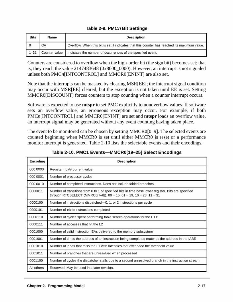
t; thatnaled
itionttingurs.
eboth
.
ts arenceings.
Counters are considered to overflow when the high-order bit (the sign bit) becomes seis, they reach the value 2147483648 (0x8000_0000). However, an interrupt is not sigunless both PMCn[INTCONTROL] and MMCR0[ENINT] are also set.
Note that the interrupts can be masked by clearing MSR[EE]; the interrupt signal condmay occur with MSR[EE] cleared, but the exception is not taken until EE is set. SeMMCR0[DISCOUNT] forces counters to stop counting when a counter interrupt occ
Software is expected to usemtspr to set PMC explicitly to nonoverflow values. If softwarsets an overflow value, an erroneous exception may occur. For example, ifPMCn[INTCONTROL] and MMCR0[ENINT] are set andmtspr loads an overflow value,an interrupt signal may be generated without any event counting having taken place
The event to be monitored can be chosen by setting MMCR0[0–9]. The selected evencounted beginning when MMCR0 is set until either MMCR0 is reset or a performamonitor interrupt is generated. Table 2-10 lists the selectable events and their encod
Table 2-9. PMCn Bit Settings
Bits Name Description
0 OV Overflow. When this bit is set it indicates that this counter has reached its maximum value.
1–31 Counter value Indicates the number of occurrences of the specified event.
Table 2-10. PMC1 Events—MMCR0[19–25] Select Encodings
Encoding Description
000 0000 Register holds current value.
000 0001 Number of processor cycles
000 0010 Number of completed instructions. Does not include folded branches.
0000011 Number of transitions from 0 to 1 of specified bits in time base lower register. Bits are specifiedthrough RTCSELECT (MMRC0[7–8]). 00 = 15, 01 = 19, 10 = 23, 11 = 31
0000100 Number of instructions dispatched—0, 1, or 2 instructions per cycle
0000101 Number of eieio instructions completed
0000110 Number of cycles spent performing table search operations for the ITLB
0000111 Number of accesses that hit the L2
0001000 Number of valid instruction EAs delivered to the memory subsystem
0001001 Number of times the address of an instruction being completed matches the address in the IABR
0001010 Number of loads that miss the L1 with latencies that exceeded the threshold value
0001011 Number of branches that are unresolved when processed
0001100 Number of cycles the dispatcher stalls due to a second unresolved branch in the instruction stream
All others Reserved. May be used in a later revision.
Chapter 2. Programming Model 2-17

Bits MMCR0[26–31] specify events associated with PMC2, as shown in Table 2-11.
Bits MMCR1[0–4] specify events associated with PMC3, as shown in Table 2-12.
Table 2-11. PMC2 Events—MMCR0[26–31] Select Encodings
Encoding Description
00 0000 Register holds current value.
00 0001 Number of processor cycles
00 0010 Number of completed instructions. Does not include folded branches.
00 0011 Number of transitions from 0 to 1 of specified bits in time base lower register. Bits are specifiedthrough RTCSELECT (MMRC0[7–8]). 00 = 15, 01 = 19, 10 = 23, 11 = 31.
00 0100 Number of instructions dispatched. 0, 1, or 2 instructions per cycle
00 0101 Number of eieio instructions completed
00 0110 Number of cycles spent performing table search operations for the ITLB
00 0111 Number of accesses that hit the L2
00 1000 Number of valid instruction EAs delivered to the memory subsystem
00 1001 Number of times that the address of an instruction being completed matches the address in the IABR
00 1010 Number of loads that miss the L1 and have latencies that exceeded the threshold value
00 1011 Number of branches that are unresolved when processed
00 1100 Number of cycles the dispatcher stalls due to a second unresolved branch in the instruction stream
All others Reserved. May be used in a later revision.
Table 2-12. PMC3 Events—MMCR1[0–4] Select Encodings
Encoding Description
0 0000 Register holds current value.
0 0001 Number of processor cycles
0 0010 Number of completed instructions, not including folded branches.
0 0011 Number of transitions from 0 to 1 of specified bits in the time base lower register. Bits are specifiedthrough RTCSELECT (MMRC0[7–8]). 0 = 47, 1 = 51, 2 = 55, 3 = 63.
0 0100 Number of instructions dispatched. 0, 1, or 2 per cycle.
0 0101 Number of L1 data cache misses
0 0110 Number of DTLB misses
0 0111 Number of L2 data misses
0 1000 Number of taken branches, including predicted branches.
0 1001 Number of transitions between marked and unmarked processes while in user mode. That is, thenumber of MSR[PM] toggles while the processor is in user mode.
0 1010 Number of store conditional instructions completed
2-18 IBM PowerPC 740 / PowerPC 750 RISC Microprocessor User’s Manual

Bits MMCR1[5–9] specify events associated with PMC4, as shown in Table 2-13.
0 1011 Number of instructions completed from the FPU
0 1100 Number of L2 castouts caused by snoops to modified lines
0 1101 Number of cache operations that hit in the L2 cache
0 1110 Reserved
0 1111 Number of cycles generated by L1 load misses
1 0000 Number of branches in the second speculative stream that resolve correctly
1 0001 Number of cycles the BPU stalls due to LR or CR unresolved dependencies
All others Reserved. May be used in a later revision.
Table 2-13. PMC4 Events—MMCR1[5–9] Select Encodings
Encoding Comments
00000 Register holds current value
00001 Number of processor cycles
00010 Number of completed instructions, not including folded branches
00011 Number of transitions from 0 to 1 of specified bits in the time base lower register. Bits are specifiedthrough RTCSELECT (MMRC0[7–8]). 0 = 47, 1 = 51, 2 = 55, 3 = 63.
00100 Number of instructions dispatched. 0, 1, or 2 per cycle.
00101 Number of L2 castouts
00110 Number of cycles spent performing tables searches for DTLB accesses
00111 Reserved. May be used in a later revision.
01000 Number of mispredicted branches
01001 Number of transitions between marked and unmarked processes while in user mode. That is, thenumber of MSR[PM] toggles while the processor is in supervisor mode.
01010 Number of store conditional instructions completed with reservation intact
01011 Number of completed sync instructions
01100 Number of snoop request retries
01101 Number of completed integer operations
01110 Number of cycles the BPU cannot process new branches due to having two unresolved branches
All others Reserved. May be used in a later revision.
Table 2-12. PMC3 Events—MMCR1[0–4] Select Encodings (Continued)
Encoding Description
Chapter 2. Programming Model 2-19
:
ad by
ntainsessor
s the.
event,an be
SIA
-level,ose959;
The PMC registers can be accessed withmtspr andmfspr using following SPR numbers
• PMC1 is SPR 953• PMC2 is SPR 954• PMC3 is SPR 957• PMC4 is SPR 958
2.1.2.4.6 User Performance Monitor Counter Registers (UPMC1–UPMC4)The contents of the PMC1–PMC4 are reflected to UPMC1–UPMC4, which can be reuser-level software. The UPMC registers can be read withmfspr using the following SPRnumbers:
• UPMC1 is SPR 937• UPMC2 is SPR 938• UPMC3 is SPR 941• UPMC4 is SPR 942
2.1.2.4.7 Sampled Instruction Address Register (SIA)The sampled instruction address register (SIA) is a supervisor-level register that cothe effective address of an instruction executing at or around the time that the procsignals the performance monitor interrupt condition. The SIA is shown in Figure 2-8.
Figure 2-8. Sampled Instruction Address Registers (SIA)
If the performance monitor interrupt is triggered by a threshold event, the SIA containexact instruction (called the sampled instruction) that caused the counter to overflow
If the performance monitor interrupt was caused by something besides a thresholdthe SIA contains the address of the last instruction completed during that cycle. SIA caccessed with themtspr andmfspr instructions using SPR 955.
2.1.2.4.8 User Sampled Instruction Address Register (USIA)The contents of SIA are reflected to USIA, which can be read by user-level software. Ucan be accessed with themfspr instructions using SPR 939.
2.1.2.4.9 Sampled Data Address Register (SDA) and User Sampled DataAddress Register (USDA)
The 750 does not implement the sampled data address register (SDA) or the userread-only USDA registers. However, for compatibility with processors that do, thregisters can be written to by boot code without causing an exception. SDA is SPRUSDA is SPR 943.
0 31
Instruction Address
2-20 IBM PowerPC 740 / PowerPC 750 RISC Microprocessor User’s Manual

thentrolevel
theeen
ions
ionion
.
eshold
2.1.3 Instruction Cache Throttling Control Register (ICTC)Reducing the rate of instruction fetching can control junction temperature withoutcomplexity and overhead of dynamic clock control. System software can coinstruction forwarding by writing a nonzero value to the ICTC register, a supervisor-lregister shown in Figure 2-9. The overall junction temperature reduction comes fromdynamic power management of each functional unit when the 750 is idle in betwinstruction fetches. PLL (phase-locked loop) and DLL (delay-locked loop) configuratare unchanged.
Figure 2-9. Instruction Cache Throttling Control Register (ICTC)
Table 2-14 describes the bit fields for the ICTC register.
Instruction cache throttling is enabled by setting ICTC[E] and writing the instructforwarding interval into ICTC[FI]. Enabling, disabling, and changing the instructforwarding interval affect instruction forwarding immediately.
The ICTC register can be accessed with themtspr andmfspr instructions using SPR 1019
2.1.4 Thermal Management Registers (THRM1–THRM3)The on-chip thermal management assist unit provides the following functions:
• Compares the junction temperature against user programmed thresholds
• Generates a thermal management interrupt if the temperature crosses the thr
• Provides a way for a successive approximation routine to estimate junctiontemperature
Table 2-14. ICTC Bit Settings
Bits Name Description
0–22 — Reserved
23–30 FI Instruction forwarding interval expressed in processor clocks.0x00 0 clock cycle.0x01 1 clock cycle..0xFF 255 clock cycles
31 E Cache throttling enable0 Disable instruction cache throttling.1 Enable instruction cache throttling.
0 22 23 30 31
EFI0 0000000000000000000000
Reserved
Chapter 2. Programming Model 2-21

ilegedintwo
ftwaren useone
oingearedand
Control and access to the thermal management assist unit is through the privmtspr/mfspr instructions to the three THRM registers. THRM1 and THRM2, shownFigure 2-10, provide the ability to compare the junction temperature againstuser-provided thresholds. Having dual thresholds allows thermal management sodiffering degrees of action in reducing junction temperature. Thermal management caa single-threshold mode in which the thermal sensor output is compared to onlythreshold in either THRM1 or THRM2.
Figure 2-10. Thermal Management Registers 1–2 (THRM1–THRM2)
The bits in THRM1 and THRM2 are described in Table 2-15.
If an mtspr affects a THRM register that contains operating parameters for an ongcomparison during operation of the thermal assist unit, the respective TIV bits are cland the comparison is restarted. Changing THRM3 forces the TIV bits of both THRM1THRM2 to 0, and restarts the comparison if THRM3[E] is set.
Table 2-15. THRM1–THRM2 Bit Settings
Bits Field Description
0 TIN Thermal management interrupt bit. Read-only. This bit is set if the thermal sensor output crossesthe threshold specified in the SPR. The state of TIN is valid only if TIV is set. The interpretation ofTIN is controlled by TID. See Table 2-16.
1 TIV Thermal management interrupt valid. Read-only. This bit is set by the thermal assist logic toindicate that the thermal management interrupt (TIN) state is valid. See Table 2-16.
2–8 Threshold Threshold that the thermal sensor output is compared to. The range is 0 —127 C, and each bitrepresents 1 C. Note that this is not the resolution of the thermal sensor.
9–28 — Reserved. System software should clear these bits when writing to the THRMn SPRs.
29 TID Thermal management interrupt direction bit. Selects the result of the temperature comparison toset TIN and to assert a thermal management interrupt if TIE is set. If TID is cleared, TIN is set andan interrupt occurs if the junction temperature exceeds the threshold. If TID is set, TIN is set andan interrupt is indicated if the junction temperature is below the threshold. See Table 2-16.
30 TIE Thermal management interrupt enable. The thermal management interrupt is maskable by theMSR[EE] bit. If TIE is cleared and THRMn is valid, the TIN bit records the status of the junctiontemperature vs. threshold comparison without causing an exception. This lets system softwaresuccessively approximate the junction temperature. See Table 2-16.
31 V SPR valid bit. Setting this bit indicates the SPR contains a valid threshold, TID and TIE controlsbits. THRM1/2[V] = 1 and THRM3[E] = 1 enables the thermal sensor operation. See Table 2-16.
TIV THRESHOLD
0 1 2 8 9 28 29 30 31
TIDTIN
Reserved
TIE V0 0000000000000000000
2-22 IBM PowerPC 740 / PowerPC 750 RISC Microprocessor User’s Manual
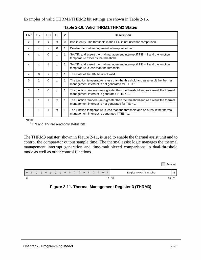
nd toermalshold
Examples of valid THRM1/THRM2 bit settings are shown in Table 2-16.
The THRM3 register, shown in Figure 2-11, is used to enable the thermal assist unit acontrol the comparator output sample time. The thermal assist logic manages the thmanagement interrupt generation and time-multiplexed comparisons in dual-thremode as well as other control functions.
Figure 2-11. Thermal Management Register 3 (THRM3)
Table 2-16. Valid THRM1/THRM2 States
TIN1
1 TIN and TIV are read-only status bits.
TIV1 TID TIE V Description
x x x x 0 Invalid entry. The threshold in the SPR is not used for comparison.
x x x 0 1 Disable thermal management interrupt assertion.
x x 0 x 1 Set TIN and assert thermal management interrupt if TIE = 1 and the junctiontemperature exceeds the threshold.
x x 1 x 1 Set TIN and assert thermal management interrupt if TIE = 1 and the junctiontemperature is less than the threshold.
x 0 x x 1 The state of the TIN bit is not valid.
0 1 0 x 1 The junction temperature is less than the threshold and as a result the thermalmanagement interrupt is not generated for TIE = 1.
1 1 0 x 1 The junction temperature is greater than the threshold and as a result the thermalmanagement interrupt is generated if TIE = 1.
0 1 1 x 1 The junction temperature is greater than the threshold and as a result the thermalmanagement interrupt is not generated for TIE = 1.
1 1 1 x 1 The junction temperature is less than the threshold and as a result the thermalmanagement interrupt is generated if TIE = 1.
Note :
0 17 18 30 31
Reserved
ESampled Interval Timer Value0 00000000000000000
Chapter 2. Programming Model 2-23

vel,d by a
The
The bits in THRM3 are described in Table 2-17.
The THRM registers can be accessed with themtspr and mfspr instructions using thefollowing SPR numbers:
• THRM1 is SPR 1020• THRM2 is SPR 1021• THRM3 is SPR 1022
2.1.5 L2 Cache Control Register (L2CR)The L2 cache control register, shown in Figure 2-12, is a supervisor-leimplementation-specific SPR used to configure and operate the L2 cache. It is clearehard reset or power-on reset.
Figure 2-12 . L2 Cache Control Register (L2CR)
The L2 cache interface is described in Chapter 9, “L2 Cache Interface Operation.”L2CR bits are described in Table 2-18.
Table 2-17. THRM3 Bit Settings
Bits Name Description
0–17 — Reserved for future use. System software should clear these bits when writing to the THRM3.
18–30 SITV Sample interval timer value. Number of elapsed processor clock cycles before a junctiontemperature vs. threshold comparison result is sampled for TIN bit setting and interruptgeneration. This is necessary due to the thermal sensor, DAC, and the analog comparatorsettling time being greater than the processor cycle time. The value should be configured to allowa sampling interval of 20 microseconds.
31 E Enables the thermal sensor compare operation if either THRM1[V] or THRM2[V] is set.
L2SIZ L2CLK L2RAM L2OH
0 1 2 3 4 6 7 8 9 10 11 12 13 14 15 16 17 18 19 30 31
L2E
L2PEL2WT
L2I
L2DR L2CTL L2TS L2SLL2DF
L2BYP L2IPReservedL2DRO
L2CS
000
21 22 23 24
L2CTR
2-24 IBM PowerPC 740 / PowerPC 750 RISC Microprocessor User’s Manual

Table 2-18. L2CR Bit Settings
Bit Name Function
0 L2E L2 enable. Enables L2 cache operation (including snooping) starting with the next transaction the L2cache unit receives. Before enabling the L2 cache, the L2 clock must be configured throughL2CR[2CLK], and the L2 DLL must stabilize (see the hardware specifications). All other L2CR bitsmust be set appropriately. The L2 cache may need to be invalidated globally.
1 L2PE L2 data parity generation and checking enable. Enables parity generation and checking for the L2data RAM interface. When disabled, generated parity is always zeros.0 Prevents L2 data parity checking.1 Allows data parity error on the L2 bus to cause a checkstop if msr(ME)=0, or a machine check
interrupt if mas(ME)=1.
2–3 L2SIZ L2 size—Should be set according to the size of the L2 data RAMs used. A 256-Kbyte L2 cacherequires a data RAM configuration of 32 Kbytes x 64 bits; a 512-Kbyte L2 cache requires aconfiguration of 64 Kbyte x 64 bits; a 1-Mbyte L2 cache requires a configuration of 128K x 64 bits.00 Reserved01 256 Kbyte10 512 Kbyte11 1 Mbyte
4–6 L2CLK L2 clock ratio (core-to-L2 frequency divider). Specifies the clock divider ratio based from the coreclock frequency that the L2 data RAM interface is to operate at. When these bits are cleared, the L2clock is stopped and the on-chip DLL for the L2 interface is disabled. For nonzero values, theprocessor generates the L2 clock and the on-chip DLL is enabled. After the L2 clock ratio is chosen,the DLL must stabilize before the L2 interface can be enabled. (See the hardware specifications). Theresulting L2 clock frequency cannot be slower than the clock frequency of the 60x bus interface.000 L2 clock and DLL disabled001 ÷1010 ÷1.5011 Reserved100 ÷2101 ÷2.5110 ÷3111 Reserved
7–8 L2RAM L2 RAM type—Configures the L2 RAM interface for the type of synchronous SRAMs used:• Flow-through (register-buffer) synchronous burst SRAMs that clock addresses in and flow data out• Pipelined (register-register) synchronous burst SRAMs that clock addresses in and clock data out• Late-write synchronous SRAMs, for which the 750 requires a pipelined (register-register)
configuration. Late-write RAMs require write data to be valid on the cycle after WE is asserted,rather than on the same cycle as the write enable as with traditional burst RAMs.
For burst RAM selections, the 750 does not burst data into the L2 cache, it generates an address foreach access. Pipelined SRAMs may be used for all L2 clock modes. Note that flow-through SRAMscan be used only for L2 clock modes divide-by-2 or slower (divide-by-1 and divide-by-1.5 notallowed).00 Flow-through (register-buffer) synchronous burst SRAM01 Reserved10 Pipelined (register-register) synchronous burst SRAM11 Pipelined (register-register) synchronous late-write SRAM
9 L2DO L2 data-only. Setting this bit enables data-only operation in the L2 cache. For this operation, onlytransactions from the L1 data cache can be cached in the L2 cache, which treats all transactions fromthe L1 instruction cache as cache-inhibited (bypass L2 cache, no L2 checking done). This bit isprovided for L2 testing only.
10 L2I L2 global invalidate. Setting L2I invalidates the L2 cache globally by clearing the L2 bits includingstatus bits. This bit must not be set while the L2 cache is enabled.
Chapter 2. Programming Model 2-25

11 L2CTL L2 RAM control (ZZ enable). Setting L2CTL enables the automatic operation of the L2ZZ (low-powermode) signal for cache RAMs that support the ZZ function. While L2CTL is asserted, L2ZZ assertsautomatically when the 750 enters nap or sleep mode and negates automatically when the 750 exitsnap or sleep mode. This bit should not be set when the 750 is in nap mode and snooping is to beperformed through deassertion of QACK. Additionally, the relatively long recovery time from ZZnegation that many SRAM vendors require may only allow use of this function for deep-sleepoperation.
12 L2WT L2 write-through. Setting L2WT selects write-through mode (rather than the default write-back mode)so all writes to the L2 cache also write through to the 60x bus. For these writes, the L2 cache entry isalways marked as clean (valid unmodified) rather than dirty (valid modified). This bit must never beasserted after the L2 cache has been enabled as previously-modified lines can get remarked asclean during normal operation.
13 L2TS L2 test support. Setting L2TS causes cache block pushes from the L1 data cache that result fromdcbf and dcbst instructions to be written only into the L2 cache and marked valid, rather than beingwritten only to the 60x bus and marked invalid in the L2 cache in case of hit. This bit allows adcbz /dcbf instruction sequence to be used with the L1 cache enabled to easily initialize the L2 cachewith any address and data information. This bit also keeps dcbz instructions from being broadcast onthe 60x and single-beat cacheable store misses in the L2 from being written to the 60x bus.
14–15 L2OH L2 output hold. These bits configure output hold time for address, data, and control signals driven bythe 750 to the L2 data RAMs. They should generally be set according to the SRAM’s input hold timerequirements, for which late-write SRAMs usually differ from flow-through or burst SRAMs.00 0.5 nS01 1.0 nS1x Reserved
16 L2SL L2 DLL slow. Setting L2SL increases the delay of each tap of the DLL delay line. It is intended toincrease the delay through the DLL to accommodate slower L2 RAM bus frequencies. Generally,L2SL should be set if the L2 RAM interface is operated below 100 MHz.
17 L2DF L2 differential clock. Setting L2DF configures the two clock-out signals (L2CLK_OUTA andL2CLK_OUTB) of the L2 interface to operate as one differential clock. In this mode, the B clock isdriven as the logical complement of the A clock. This mode supports the differential clockrequirements of late-write SRAMs. Generally, this bit should be set when late-write SRAMs are used.
18 L2BYP L2 DLL bypass. The DLL unit receives three input clocks:• A square-wave clock from the PLL unit to phase adjust and export• A non-square-wave clock for the internal phase reference• A feedback clock (L2SYNC_IN) for the external phase reference.Asserting L2BYP causes clock #2 to be used as clocks #1 and #2. (Clock #2 is the actual clock usedby the registers of the L2 interface circuitry.) L2BYP is intended for use when the PLL is beingbypassed, and for engineering evaluation. If the PLL is being bypassed, the DLL must be operated individe-by-1 mode, and SYSCLK must be fast enough for the DLL to support.
19–21 — Reserved. These bits are implemented but not used; keep at 0 for future compatibility.
22 L2CS L2 Clock Stop (for chip revisions 3.0 and later). Asserting this bit causes the L2 clocks to the SRAMSto be automatically stopped whenever the 750 enters nap or sleep modes, and automaticallyrestarted when exiting those modes (including snooping during nap mode). The L2SYNC_OUT/SYNC_IN path will remain operating to keep the DLL in sync. This bit is provided as apower-saving alternative to the L2CTL bit and its corresponding ZZ pin, which may not be useful fordynamic stopping/restarting of the L2 interface from nap and sleep modes due to the relatively longrecovery time from ZZ negation that many SRAM vendors require.
Table 2-18. L2CR Bit Settings (Continued)
Bit Name Function
2-26 IBM PowerPC 740 / PowerPC 750 RISC Microprocessor User’s Manual

.
The L2CR register can be accessed with themtspr andmfspr instructions using SPR 101723 L2DRO L2 DLL Rollover Checkstop Enable (for chip revisions 3.0 and later). Asserting this bit enables apotential/actual rollover condition of the DLL to cause a checkstop for the processor. A potentialrollover condition occurs when the DLL is selecting the last tap of the delay line, and thus may riskrolling over to the first tap with one adjustment while in the process of keeping in sync. Such acondition is improper operation for the DLL, and while this condition is not expected, this bit allowsdetection for added security. This bit should be set when the DLL is first enabled (set with the L2CLKbits) to detect rollover during initial synchronization. It could also be set when the L2 cache is enabled(with L2E bit) after the DLL has achieved initial lock.0 Prevents DLL rollover to checkstop.1 Enable a rollover or terminal count of the DLL to checkstop the processor (independent of
MSR(ME) bit.
24-30 L2CTR L2 DLL counter value (read only; for chip revisions 3.0 and later). These bits indicate the currentvalue of the DLL counter (0 to 127). They are asynchronously read when the L2CR is read, and assuch, should be read at least twice with the same value in case the value is asynchronously caught intransition. These bits are intended to provide observability of where in the 128-bit delay chain the DLLis at any given time. Generally, the DLL operation should be considered at risk if it is found to bewithin a couple of taps of its beginning or end point (tap 0 or tap 128).
31 L2IP L2 global invalidate in progress (read only). This read-only bit indicates whether an L2 globalinvalidate is occurring. It should be monitored after an L2 global invalidate has been initiated by theL2I bit to determine when it has completed.
Table 2-18. L2CR Bit Settings (Continued)
Bit Name Function
Chapter 2. Programming Model 2-27
s of thetions, and
ndard. Theoth)metic
but
sion
oneitly
ls tos foring
eticxtra
econding
dress
/stores of a
2.2 Operand ConventionsThis section describes the operand conventions as they are represented in two levelPowerPC architecture—UISA and VEA. Detailed descriptions are provided of convenused for storing values in registers and memory, accessing PowerPC registersrepresentation of data in these registers.
2.2.1 Floating-Point Execution Models—UISAThe IEEE 754 standard defines conventions for 64- and 32-bit arithmetic. The starequires that single-precision arithmetic be provided for single-precision operandsstandard permits double-precision arithmetic instructions to have either (or bsingle-precision or double-precision operands, but states that single-precision arithinstructions should not accept double-precision operands.
The PowerPC UISA follows these guidelines:
• Double-precision arithmetic instructions may have single-precision operands always produce double-precision results.
• Single-precision arithmetic instructions require all operands to be single-preciand always produce single-precision results.
For arithmetic instructions, conversion from double- to single-precision must be dexplicitly by software, while conversion from single- to double-precision is done implicby the processor.
All PowerPC implementations provide the equivalent of the following execution modeensure that identical results are obtained. The definition of the arithmetic instructioninfinities, denormalized numbers, and NaNs follow conventions described in the followsections.
Although the double-precision format specifies an 11-bit exponent, exponent arithmuses two additional bit positions to avoid potential transient overflow conditions. An ebit is required when denormalized double-precision numbers are prenormalized. A sbit is required to permit computation of the adjusted exponent value in the followexamples when the corresponding exception enable bit is one:
• Underflow during multiplication using a denormalized operand• Overflow during division using a denormalized divisor
2.2.2 Data Organization in Memory and Data TransfersBytes in memory are numbered consecutively starting with 0. Each number is the adof the corresponding byte.
Memory operands may be bytes, half words, words, or double words, or, for the loadmultiple and load/store string instructions, a sequence of bytes or words. The addres
2-28 IBM PowerPC 740 / PowerPC 750 RISC Microprocessor User’s Manual

yte).
ndarydth.own incause
mple,
ition,e best
notent
rationsuffer
-pointligned
ointctureEE
rand
alizedrminged byrands.
memory operand is the address of its first byte (that is, of its lowest-numbered bOperand length is implicit for each instruction.
2.2.3 Alignment and Misaligned AccessesThe operand of a single-register memory access instruction has an alignment bouequal to its length. An operand’s address is misaligned if it is not a multiple of its wiOperands for single-register memory access instructions have the characteristics shTable 2-19. Although not permitted as memory operands, quad words are shown bequad-word alignment is desirable for certain memory operands.
The concept of alignment is also applied more generally to data in memory. For exaa 12-byte data item is said to be word-aligned if its address is a multiple of four.
Some instructions require their memory operands to have certain alignment. In addalignment may affect performance. For single-register memory access instructions, thperformance is obtained when memory operands are aligned.
Instructions are 32 bits (one word) long and must be word-aligned.
The 750 does not provide hardware support for floating-point memory that isword-aligned. If a floating-point operand is not aligned, the 750 invokes an alignmexception, and it is left up to software to break up the offending storage access opeappropriately. In addition, some non-double-word–aligned memory accessesperformance degradation as compared to an aligned access of the same type.
In general, floating-point word accesses should always be word-aligned and floatingdouble-word accesses should always be double-word–aligned. Frequent use of misaaccesses is discouraged since they can degrade overall performance.
2.2.4 Floating-Point OperandThe 750 provides hardware support for all single- and double-precision floating-poperations for most value representations and all rounding modes. This architeprovides for hardware to implement a floating-point system as defined in ANSI/IEstandard 754-1985,IEEE Standard for Binary Floating Point Arithmetic. Detailedinformation about the floating-point execution model can be found in Chapter 3, “OpeConventions,” inThe Programming Environments Manual.
The 750 supports non-IEEE mode whenever FPSCR[29] is set. In this mode, denormnumbers, NaNs, and some IEEE invalid operations are treated in a non-IEEE confomanner. This is accomplished by delivering results that approximate the values requirthe IEEE standard. Table 2-19 summarizes the conditions and mode behavior for ope
Chapter 2. Programming Model 2-29

Table 2-19. Floating-Point Operand Data Type Behavior
Operand AData Type
Operand BData Type
Operand CData Type
IEEE Mode(NI = 0)
Non-IEEE Mode(NI = 1)
Single denormalizedDouble denormalized
Single denormalizedDouble denormalized
Single denormalizedDouble denormalized
Normalize all three Zero all three
Single denormalizedDouble denormalized
Single denormalizedDouble denormalized
Normalized or zero Normalize A and B Zero A and B
Normalized or zero Single denormalizedDouble denormalized
Single denormalizedDouble denormalized
Normalize B and C Zero B and C
Single denormalizedDouble denormalized
Normalized or zero Single denormalizedDouble denormalized
Normalize A and C Zero A and C
Single denormalizedDouble denormalized
Normalized or zero Normalized or zero Normalize A Zero A
Normalized or zero Single denormalizedDouble denormalized
Normalized or zero Normalize B Zero B
Normalized or zero Normalized or zero Single denormalizedDouble denormalized
Normalize C Zero C
Single QNaNSingle SNaNDouble QNaNDouble SNaN
Don’t care Don’t care QNaN1 QNaN1
Don’t care Single QNaNSingle SNaNDouble QNaNDouble SNaN
Don’t care QNaN1 QNaN1
Don’t care Don’t care Single QNaNSingle SNaNDouble QNaNDouble SNaN
QNaN1 QNaN1
Single normalizedSingle infinitySingle zeroDouble normalizedDouble infinityDouble zero
Single normalizedSingle infinitySingle zeroDouble normalizedDouble infinityDouble zero
Single normalizedSingle infinitySingle zeroDouble normalizedDouble infinityDouble zero
Do the operation Do the operation
1 Prioritize according to Chapter 3, “Operand Conventions,” in The Programming Environments Manual.
2-30 IBM PowerPC 740 / PowerPC 750 RISC Microprocessor User’s Manual
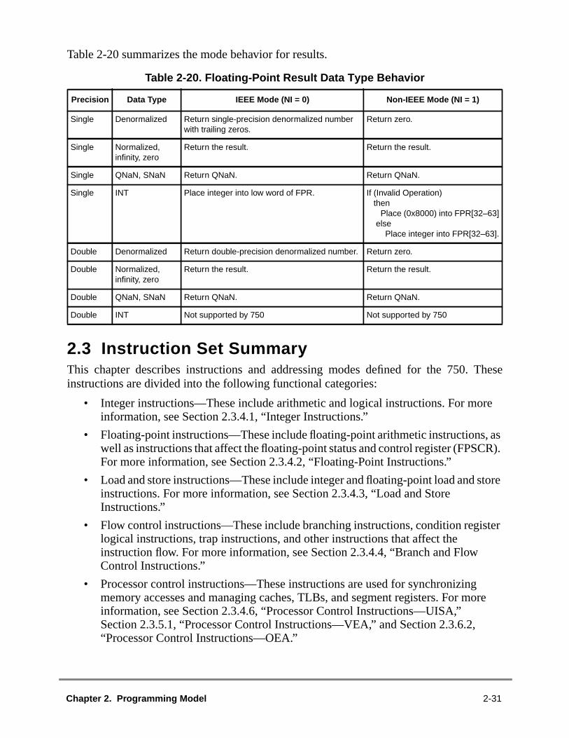
These
re
, asCR).
store
ster
ore
Table 2-20 summarizes the mode behavior for results.
2.3 Instruction Set SummaryThis chapter describes instructions and addressing modes defined for the 750.instructions are divided into the following functional categories:
• Integer instructions—These include arithmetic and logical instructions. For moinformation, see Section 2.3.4.1, “Integer Instructions.”
• Floating-point instructions—These include floating-point arithmetic instructionswell as instructions that affect the floating-point status and control register (FPSFor more information, see Section 2.3.4.2, “Floating-Point Instructions.”
• Load and store instructions—These include integer and floating-point load andinstructions. For more information, see Section 2.3.4.3, “Load and StoreInstructions.”
• Flow control instructions—These include branching instructions, condition regilogical instructions, trap instructions, and other instructions that affect theinstruction flow. For more information, see Section 2.3.4.4, “Branch and FlowControl Instructions.”
• Processor control instructions—These instructions are used for synchronizingmemory accesses and managing caches, TLBs, and segment registers. For minformation, see Section 2.3.4.6, “Processor Control Instructions—UISA,”Section 2.3.5.1, “Processor Control Instructions—VEA,” and Section 2.3.6.2,“Processor Control Instructions—OEA.”
Table 2-20. Floating-Point Result Data Type Behavior
Precision Data Type IEEE Mode (NI = 0) Non-IEEE Mode (NI = 1)
Single Denormalized Return single-precision denormalized numberwith trailing zeros.
Return zero.
Single Normalized,infinity, zero
Return the result. Return the result.
Single QNaN, SNaN Return QNaN. Return QNaN.
Single INT Place integer into low word of FPR. If (Invalid Operation)then
Place (0x8000) into FPR[32–63]else
Place integer into FPR[32–63].
Double Denormalized Return double-precision denormalized number. Return zero.
Double Normalized,infinity, zero
Return the result. Return the result.
Double QNaN, SNaN Return QNaN. Return QNaN.
Double INT Not supported by 750 Not supported by 750
Chapter 2. Programming Model 2-31

ry
Bs,ntrol.”
rnal
it thatsefulg.”
te onctureord,
urposetores
ts ofation,target
ands.bols
fied
cs asfor thein that
erPCerPC
• Memory synchronization instructions—These instructions are used for memosynchronizing. See Section 2.3.4.7, “Memory SynchronizationInstructions—UISA,” Section 2.3.5.2, “Memory SynchronizationInstructions—VEA,” for more information.
• Memory control instructions—These instructions provide control of caches, TLand segment registers. For more information, see Section 2.3.5.3, “Memory CoInstructions—VEA,” and Section 2.3.6.3, “Memory Control Instructions—OEA
• External control instructions—These include instructions for use with specialinput/output devices. For more information, see Section 2.3.5.4, “Optional ExteControl Instructions.”
Note that this grouping of instructions does not necessarily indicate the execution unprocesses a particular instruction or group of instructions. This information, which is ufor scheduling instructions most effectively, is provided in Chapter 6, “Instruction Timin
Integer instructions operate on word operands. Floating-point instructions operasingle-precision and double-precision floating-point operands. The PowerPC architeuses instructions that are four bytes long and word-aligned. It provides for byte, half-wand word operand loads and stores between memory and a set of 32 general-pregisters (GPRs). It also provides for word and double-word operand loads and sbetween memory and a set of 32 floating-point registers (FPRs).
Arithmetic and logical instructions do not read or modify memory. To use the contena memory location in a computation and then modify the same or another memory locthe memory contents must be loaded into a register, modified, and then written to thelocation using load and store instructions.
The description of each instruction includes the mnemonic and a formatted list of operTo simplify assembly language programming, a set of simplified mnemonics and symis provided for some of the frequently-used instructions; see Appendix F, “SimpliMnemonics,” inThe Programming Environments Manualfor a complete list of simplifiedmnemonics. Note that the architecture specification refers to simplified mnemoniextended mnemonics. Programs written to be portable across the various assemblersPowerPC architecture should not assume the existence of mnemonics not describeddocument.
2.3.1 Classes of InstructionsThe 750 instructions belong to one of the following three classes:
• Defined• Illegal• Reserved
Note that while the definitions of these terms are consistent among the Powprocessors, the assignment of these classifications is not. For example, Pow
2-32 IBM PowerPC 740 / PowerPC 750 RISC Microprocessor User’s Manual

-bit
if any.fined
n thes.
s ones theurioused byeeded.ions,
tions,
ll
ramay be
rs to
for
ns to
instructions defined for 64-bit implementations are treated as illegal by 32implementations such as the 750.
The class is determined by examining the primary opcode and the extended opcode,If the opcode, or combination of opcode and extended opcode, is not that of a deinstruction or of a reserved instruction, the instruction is illegal.
Instruction encodings that are now illegal may become assigned to instructions iarchitecture or may be reserved by being assigned to processor-specific instruction
2.3.1.1 Definition of Boundedly UndefinedIf instructions are encoded with incorrectly set bits in reserved fields, the resultexecution can be said to be boundedly undefined. If a user-level program executincorrectly coded instruction, the resulting undefined results are bounded in that a spchange from user to supervisor state is not allowed, and the level of privilege exercisthe program in relation to memory access and other system resources cannot be excBoundedly-undefined results for a given instruction may vary between implementatand between execution attempts in the same implementation.
2.3.1.2 Defined Instruction ClassDefined instructions are guaranteed to be supported in all PowerPC implementaexcept as stated in the instruction descriptions in Chapter 8, “Instruction Set,” inTheProgramming Environments Manual. The 750 provides hardware support for ainstructions defined for 32-bit implementations. It does not support the optionalfsqrt ,fsqrts, andtlbia instructions.
A PowerPC processor invokes the illegal instruction error handler (part of the progexception) when the unimplemented PowerPC instructions are encountered so they memulated in software, as required. Note that the architecture specification refeexceptions as interrupts.
A defined instruction can have invalid forms. The 750 provides limited supportinstructions represented in an invalid form.
2.3.1.3 Illegal Instruction ClassIllegal instructions can be grouped into the following categories:
• Instructions not defined in the PowerPC architecture.The following primaryopcodes are defined as illegal but may be used in future extensions to thearchitecture:
1, 4, 5, 6, 9, 22, 56, 57, 60, 61
Future versions of the PowerPC architecture may define any of these instructioperform new functions.
Chapter 2. Programming Model 2-33

cific4-bit750.
are
bendor
codes.)
hisorythat
lass.”
en it-bit
egalros,
es notervedSee
ailsPC
the
• Instructions defined in the PowerPC architecture but not implemented in a spePowerPC implementation. For example, instructions that can be executed on 6PowerPC processors are considered illegal by 32-bit processors such as the
The following primary opcodes are defined for 64-bit implementations only andillegal on the 750:
2, 30, 58, 62
• All unused extended opcodes are illegal. The unused extended opcodes can determined from information in Section A.2, “Instructions Sorted by Opcode,” aSection 2.3.1.4, “Reserved Instruction Class.” Notice that extended opcodes finstructions defined only for 64-bit implementations are illegal in 32-bitimplementations, and vice versa. The following primary opcodes have unusedextended opcodes.
17, 19, 31, 59, 63 (Primary opcodes 30 and 62 are illegal for all 32-bitimplementations, but as 64-bit opcodes they have some unused extended op
• An instruction consisting of only zeros is guaranteed to be an illegal instruction. Tincreases the probability that an attempt to execute data or uninitialized meminvokes the system illegal instruction error handler (a program exception). Noteif only the primary opcode consists of all zeros, the instruction is considered areserved instruction, as described in Section 2.3.1.4, “Reserved Instruction C
The 750 invokes the system illegal instruction error handler (a program exception) whdetects any instruction from this class or any instructions defined only for 64implementations.
See Section 4.5.7, “Program Exception (0x00700),” for additional information about illand invalid instruction exceptions. Except for an instruction consisting of binary zeillegal instructions are available for additions to the PowerPC architecture.
2.3.1.4 Reserved Instruction ClassReserved instructions are allocated to specific implementation-dependent purposdefined by the PowerPC architecture. Attempting to execute an unimplemented resinstruction invokes the illegal instruction error handler (a program exception).“Program Exception (0x00700),” in Chapter 6, “Exceptions,” inThe ProgrammingEnvironments Manual for information about illegal and invalid instruction exceptions.
The PowerPC architecture defines four types of reserved instructions:
• Instructions in the POWER architecture not part of the PowerPC UISA. For deton POWER architecture incompatibilities and how they are handled by Powerprocessors, see Appendix B, “POWER Architecture Cross Reference,” inTheProgramming Environments Manual.
• Implementation-specific instructions required for the processor to conform to PowerPC architecture (none of these are implemented in the 750)
• All other implementation-specific instructions
2-34 IBM PowerPC 740 / PowerPC 750 RISC Microprocessor User’s Manual

for2-bit
er 4,
y thees the
s the
/stores of ayte).both
dian.
menterandif it
about
ing an. Forlengtharoundin the
signed
• Architecturally-allowed extended opcodes
2.3.2 Addressing ModesThis section provides an overview of conventions for addressing memory andcalculating effective addresses as defined by the PowerPC architecture for 3implementations. For more detailed information, see “Conventions,” in Chapt“Addressing Modes and Instruction Set Summary,” ofThe Programming EnvironmentsManual.
2.3.2.1 Memory AddressingA program references memory using the effective (logical) address computed bprocessor when it executes a memory access or branch instruction or when it fetchnext sequential instruction.
Bytes in memory are numbered consecutively starting with zero. Each number iaddress of the corresponding byte.
2.3.2.2 Memory OperandsMemory operands may be bytes, half words, words, or double words, or, for the loadmultiple and load/store string instructions, a sequence of bytes or words. The addresmemory operand is the address of its first byte (that is, of its lowest-numbered bOperand length is implicit for each instruction. The PowerPC architecture supportsbig-endian and little-endian byte ordering. The default byte and bit ordering is big-enSee “Byte Ordering,” in Chapter 3, “Operand Conventions,” ofThe ProgrammingEnvironments Manual for more information about big- and little-endian byte ordering.
The operand of a single-register memory access instruction has a natural alignboundary equal to the operand length. In other words, the “natural” address of an opis an integral multiple of the operand length. A memory operand is said to be alignedis aligned at its natural boundary; otherwise it is misaligned. For a detailed discussionmemory operands, see Chapter 3, “Operand Conventions,” ofThe ProgrammingEnvironments Manual.
2.3.2.3 Effective Address CalculationAn effective address is the 32-bit sum computed by the processor when executmemory access or branch instruction or when fetching the next sequential instructioa memory access instruction, if the sum of the effective address and the operandexceeds the maximum effective address, the memory operand is considered to wrapfrom the maximum effective address through effective address 0, as describedfollowing paragraphs.
Effective address computations for both data and instruction accesses use 32-bit unbinary arithmetic. A carry from bit 0 is ignored.
Chapter 2. Programming Model 2-35

:
x)
tailed
that is
ing
use
n is
and
d
r to
havees, butnt. For
ld beode.
Load and store operations have the following modes of effective address generation
• EA = (rA|0) + offset (including offset = 0) (register indirect with immediate inde• EA = (rA|0) + rB (register indirect with index)
Refer to Section 2.3.4.3.2, “Integer Load and Store Address Generation,” for a dedescription of effective address generation for load and store operations.
Branch instructions have three categories of effective address generation:
• Immediate• Link register indirect• Count register indirect
2.3.2.4 SynchronizationThe synchronization described in this section refers to the state of the processorperforming the synchronization.
2.3.2.4.1 Context SynchronizationThe System Call (sc) and Return from Interrupt (rfi ) instructions perform contextsynchronization by allowing previously issued instructions to complete before performa change in context. Execution of one of these instructions ensures the following:
• No higher priority exception exists (sc).
• All previous instructions have completed to a point where they can no longer caan exception. If a prior memory access instruction causes direct-store errorexceptions, the results are guaranteed to be determined before this instructioexecuted.
• Previous instructions complete execution in the context (privilege, protection, address translation) under which they were issued.
• The instructions following thescor rfi instruction execute in the context establisheby these instructions.
2.3.2.4.2 Execution SynchronizationAn instruction is execution synchronizing if all previously initiated instructions appeahave completed before the instruction is initiated or, in the case ofsyncandisync, beforethe instruction completes. For example, the Move to Machine State Register (mtmsr)instruction is execution synchronizing. It ensures that all preceding instructionscompleted execution and cannot cause an exception before the instruction executdoes not ensure subsequent instructions execute in the newly established environmeexample, if themtmsr sets the MSR[PR] bit, unless anisync immediately follows themtmsr instruction, a privileged instruction could be executed or privileged access couperformed without causing an exception even though the MSR[PR] bit indicates user m
2-36 IBM PowerPC 740 / PowerPC 750 RISC Microprocessor User’s Manual

of ancause
rame theramvel
s
D1
r DSI
t
r.
”
750culared in
d fortecture
d.
2.3.2.4.3 Instruction-Related ExceptionsThere are two kinds of exceptions in the 750—those caused directly by the executioninstruction and those caused by an asynchronous event (or interrupts). Either maycomponents of the system software to be invoked.
Exceptions can be caused directly by the execution of an instruction as follows:
• An attempt to execute an illegal instruction causes the illegal instruction (progexception) handler to be invoked. An attempt by a user-level program to executsupervisor-level instructions listed below causes the privileged instruction (progexception) handler to be invoked. The 750 provides the following supervisor-leinstructions:dcbi, mfmsr, mfspr, mfsr, mfsrin , mtmsr, mtspr, mtsr, mtsrin , rfi ,tlbie, andtlbsync. Note that the privilege level of themfspr andmtspr instructionsdepends on the SPR encoding.
• Any mtspr, mfspr, ormftb instruction with an invalid SPR (or TBR) field causean illegal type program exception. Likewise, a program exception is taken ifuser-level software tries to access a supervisor-level SPR. Anmtspr instructionexecuting in supervisor mode (MSR[PR] = 0) with the SPR field specifying HIor PVR (read-only registers) executes as a no-op.
• An attempt to access memory that is not available (page fault) causes the ISI oexception handler to be invoked.
• The execution of ansc instruction invokes the system call exception handler thapermits a program to request the system to perform a service.
• The execution of a trap instruction invokes the program exception trap handle
• The execution of an instruction that causes a floating-point exception whileexceptions are enabled in the MSR invokes the program exception handler.
A detailed description of exception conditions is provided in Chapter 4, “Exceptions.
2.3.3 Instruction Set OverviewThis section provides a brief overview of the PowerPC instructions implemented in theand highlights any special information with respect to how the 750 implements a partiinstruction. Note that the categories used in this section correspond to those usChapter 4, “Addressing Modes and Instruction Set Summary,” inThe ProgrammingEnvironments Manual. These categorizations are somewhat arbitrary and are providethe convenience of the programmer and do not necessarily reflect the PowerPC archispecification.
Note that some instructions have the following optional features:
• CR Update—The dot (.) suffix on the mnemonic enables the update of the CR.• Overflow option—Theo suffix indicates that the overflow bit in the XER is enable
Chapter 2. Programming Model 2-37
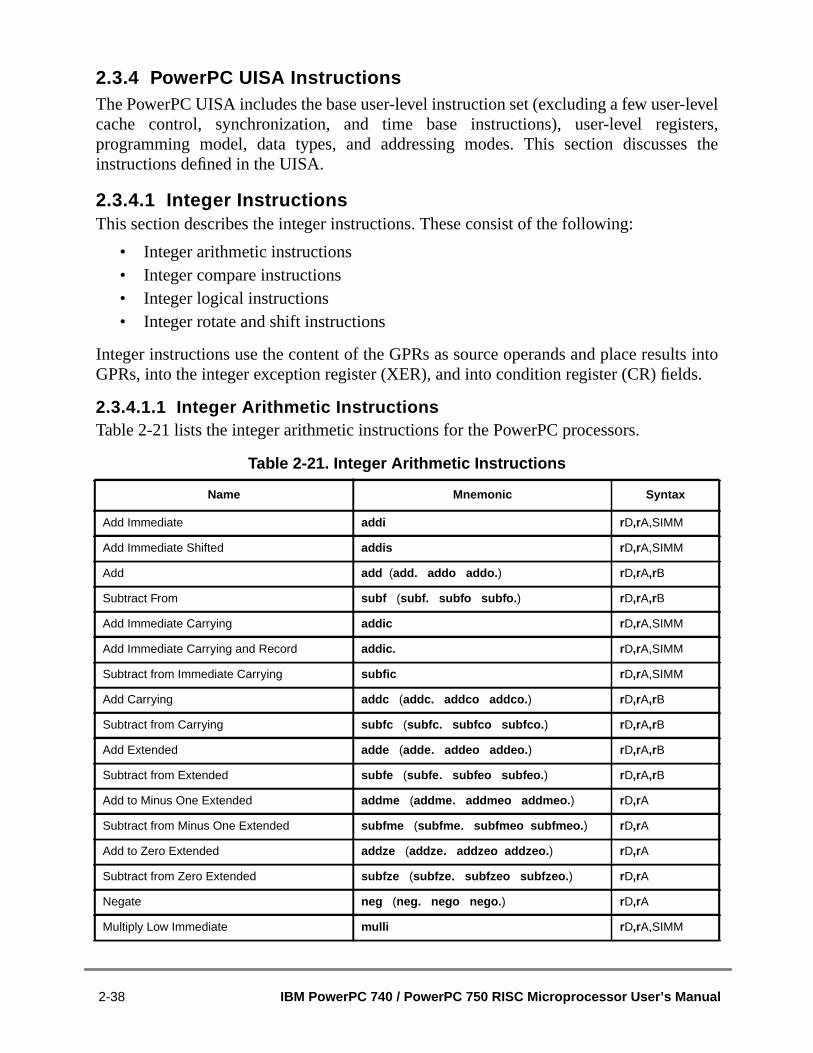
-levelsters,es the
lts intods.
2.3.4 PowerPC UISA InstructionsThe PowerPC UISA includes the base user-level instruction set (excluding a few usercache control, synchronization, and time base instructions), user-level regiprogramming model, data types, and addressing modes. This section discussinstructions defined in the UISA.
2.3.4.1 Integer InstructionsThis section describes the integer instructions. These consist of the following:
• Integer arithmetic instructions• Integer compare instructions• Integer logical instructions• Integer rotate and shift instructions
Integer instructions use the content of the GPRs as source operands and place resuGPRs, into the integer exception register (XER), and into condition register (CR) fiel
2.3.4.1.1 Integer Arithmetic InstructionsTable 2-21 lists the integer arithmetic instructions for the PowerPC processors.
Table 2-21. Integer Arithmetic Instructions
Name Mnemonic Syntax
Add Immediate addi r D,rA,SIMM
Add Immediate Shifted addis r D,rA,SIMM
Add add (add. addo addo. ) rD,rA,rB
Subtract From subf (subf. subfo subfo. ) rD,rA,rB
Add Immediate Carrying addic r D,rA,SIMM
Add Immediate Carrying and Record addic. r D,rA,SIMM
Subtract from Immediate Carrying subfic r D,rA,SIMM
Add Carrying addc (addc. addco addco. ) rD,rA,rB
Subtract from Carrying subfc (subfc. subfco subfco. ) rD,rA,rB
Add Extended adde (adde. addeo addeo. ) rD,rA,rB
Subtract from Extended subfe (subfe. subfeo subfeo. ) rD,rA,rB
Add to Minus One Extended addme (addme. addmeo addmeo. ) rD,rA
Subtract from Minus One Extended subfme (subfme. subfmeo subfmeo. ) rD,rA
Add to Zero Extended addze (addze. addzeo addzeo. ) rD,rA
Subtract from Zero Extended subfze (subfze. subfzeo subfzeo. ) rD,rA
Negate neg (neg. nego nego. ) rD,rA
Multiply Low Immediate mulli r D,rA,SIMM
2-38 IBM PowerPC 740 / PowerPC 750 RISC Microprocessor User’s Manual
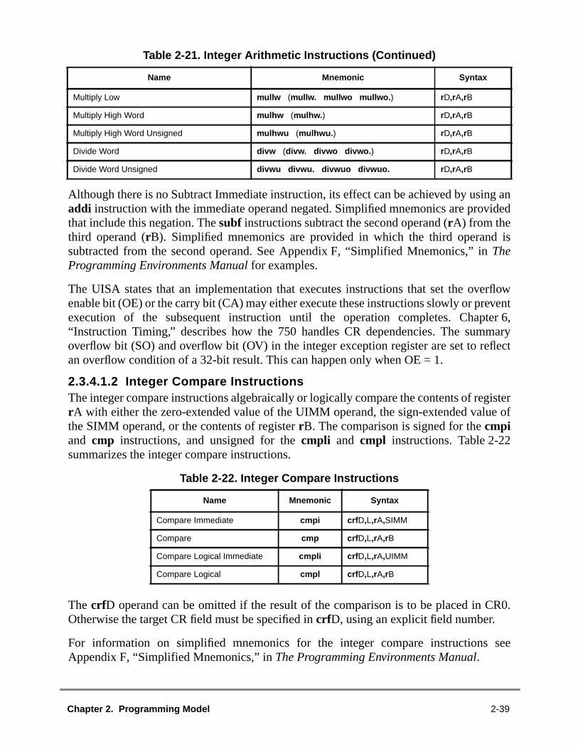
ng anided
is
rflowventter 6,maryflect
gistere of
R0.
see
Although there is no Subtract Immediate instruction, its effect can be achieved by usiaddi instruction with the immediate operand negated. Simplified mnemonics are provthat include this negation. Thesubf instructions subtract the second operand (rA) from thethird operand (rB). Simplified mnemonics are provided in which the third operandsubtracted from the second operand. See Appendix F, “Simplified Mnemonics,” inTheProgramming Environments Manual for examples.
The UISA states that an implementation that executes instructions that set the oveenable bit (OE) or the carry bit (CA) may either execute these instructions slowly or preexecution of the subsequent instruction until the operation completes. Chap“Instruction Timing,” describes how the 750 handles CR dependencies. The sumoverflow bit (SO) and overflow bit (OV) in the integer exception register are set to rean overflow condition of a 32-bit result. This can happen only when OE = 1.
2.3.4.1.2 Integer Compare InstructionsThe integer compare instructions algebraically or logically compare the contents of rerA with either the zero-extended value of the UIMM operand, the sign-extended valuthe SIMM operand, or the contents of registerrB. The comparison is signed for thecmpiand cmp instructions, and unsigned for thecmpli and cmpl instructions. Table 2-22summarizes the integer compare instructions.
The crfD operand can be omitted if the result of the comparison is to be placed in COtherwise the target CR field must be specified incrfD, using an explicit field number.
For information on simplified mnemonics for the integer compare instructionsAppendix F, “Simplified Mnemonics,” inThe Programming Environments Manual.
Multiply Low mullw (mullw. mullwo mullwo. ) rD,rA,rB
Multiply High Word mulhw (mulhw. ) rD,rA,rB
Multiply High Word Unsigned mulhwu (mulhwu. ) rD,rA,rB
Divide Word divw (divw. divwo divwo. ) rD,rA,rB
Divide Word Unsigned divwu divwu. divwuo divwuo. r D,rA,rB
Table 2-22. Integer Compare Instructions
Name Mnemonic Syntax
Compare Immediate cmpi crf D,L,rA,SIMM
Compare cmp crf D,L,rA,rB
Compare Logical Immediate cmpli crf D,L,rA,UIMM
Compare Logical cmpl crf D,L,rA,rB
Table 2-21. Integer Arithmetic Instructions (Continued)
Name Mnemonic Syntax
Chapter 2. Programming Model 2-39

the) andal
of the
tmostnd
2.3.4.1.3 Integer Logical InstructionsThe logical instructions shown in Table 2-23 perform bit-parallel operations onspecified operands. Logical instructions with the CR updating enabled (uses dot suffixinstructionsandi. and andis. set CR field CR0 to characterize the result of the logicoperation. Logical instructions do not affect XER[SO], XER[OV], or XER[CA].
See Appendix F, “Simplified Mnemonics,” inThe Programming Environments Manualforsimplified mnemonic examples for integer logical operations.
2.3.4.1.4 Integer Rotate and Shift InstructionsRotation operations are performed on data from a GPR, and the result, or a portionresult, is returned to a GPR. See Appendix F, “Simplified Mnemonics,” inTheProgramming Environments Manualfor a complete list of simplified mnemonics thaallows simpler coding of often-used functions such as clearing the leftmost or rightbits of a register, left justifying or right justifying an arbitrary field, and simple rotates ashifts.
Table 2-23. Integer Logical Instructions
Name Mnemonic Syntax Implementation Notes
AND Immediate andi. r A,rS,UIMM —
AND Immediate Shifted andis. r A,rS,UIMM —
OR Immediate ori r A,rS,UIMM The PowerPC architecture defines ori r0,r0,0 as thepreferred form for the no-op instruction. The dispatcherdiscards this instruction (except for pending trace orbreakpoint exceptions).
OR Immediate Shifted oris r A,rS,UIMM —
XOR Immediate xori r A,rS,UIMM —
XOR Immediate Shifted xoris r A,rS,UIMM —
AND and (and. ) rA,rS,rB —
OR or (or. ) rA,rS,rB —
XOR xor (xor. ) rA,rS,rB —
NAND nand (nand. ) rA,rS,rB —
NOR nor (nor. ) rA,rS,rB —
Equivalent eqv (eqv. ) rA,rS,rB —
AND with Complement andc (andc. ) rA,rS,rB —
OR with Complement orc (orc. ) rA,rS,rB —
Extend Sign Byte extsb (extsb. ) rA,rS —
Extend Sign Half Word extsh (extsh. ) rA,rS —
Count Leading Zeros Word cntlzw (cntlzw. ) rA,rS —
2-40 IBM PowerPC 740 / PowerPC 750 RISC Microprocessor User’s Manual
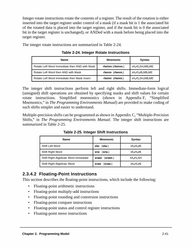
eithered bitciatedo the
calertainedf
sion
Integer rotate instructions rotate the contents of a register. The result of the rotation isinserted into the target register under control of a mask (if a mask bit is 1 the associatof the rotated data is placed into the target register, and if the mask bit is 0 the assobit in the target register is unchanged), or ANDed with a mask before being placed inttarget register.
The integer rotate instructions are summarized in Table 2-24.
The integer shift instructions perform left and right shifts. Immediate-form logi(unsigned) shift operations are obtained by specifying masks and shift values for crotate instructions. Simplified mnemonics (shown in Appendix F, “SimplifiMnemonics,” inThe Programming Environments Manual) are provided to make coding osuch shifts simpler and easier to understand.
Multiple-precision shifts can be programmed as shown in Appendix C, “Multiple-PreciShifts,” in The Programming Environments Manual. The integer shift instructions aresummarized in Table 2-25.
2.3.4.2 Floating-Point InstructionsThis section describes the floating-point instructions, which include the following:
• Floating-point arithmetic instructions• Floating-point multiply-add instructions• Floating-point rounding and conversion instructions• Floating-point compare instructions• Floating-point status and control register instructions• Floating-point move instructions
Table 2-24. Integer Rotate Instructions
Name Mnemonic Syntax
Rotate Left Word Immediate then AND with Mask rlwinm (rlwinm. ) rA,rS,SH,MB,ME
Rotate Left Word then AND with Mask rlwnm (rlwnm. ) rA,rS,rB,MB,ME
Rotate Left Word Immediate then Mask Insert rlwimi (rlwimi. ) rA,rS,SH,MB,ME
Table 2-25. Integer Shift Instructions
Name Mnemonic Syntax
Shift Left Word slw (slw. ) rA,rS,rB
Shift Right Word srw (srw. ) rA,rS,rB
Shift Right Algebraic Word Immediate srawi (srawi. ) rA,rS,SH
Shift Right Algebraic Word sraw (sraw. ) rA,rS,rB
Chapter 2. Programming Model 2-41

oint
754oint
mode
mat.isionisioncision
ding.
See Section 2.3.4.3, “Load and Store Instructions,” for information about floating-ploads and stores.
The PowerPC architecture supports a floating-point system as defined in the IEEEstandard, but requires software support to conform with that standard. All floating-poperations conform to the IEEE 754 standard, except if software sets the non-IEEEFPSCR[NI].
2.3.4.2.1 Floating-Point Arithmetic InstructionsThe floating-point arithmetic instructions are summarized in Table 2-26.
All single-precision arithmetic instructions are performed using a double-precision forThe floating-point architecture is a single-pass implementation for double-precproducts. In most cases, a single-precision instruction using only single-precoperands, in double-precision format, has the same latency as its double-preequivalent.
2.3.4.2.2 Floating-Point Multiply-Add InstructionsThese instructions combine multiply and add operations without an intermediate rounoperation. The floating-point multiply-add instructions are summarized in Table 2-27
Table 2-26. Floating-Point Arithmetic Instructions
Name Mnemonic Syntax
Floating Add (Double-Precision) fadd (fadd. ) frD,frA,frB
Floating Add Single fadds (fadds. ) frD,frA,frB
Floating Subtract (Double-Precision) fsub (fsub. ) frD,frA,frB
Floating Subtract Single fsubs (fsubs. ) frD,frA,frB
Floating Multiply (Double-Precision) fmul (fmul. ) frD,frA,frC
Floating Multiply Single fmuls (fmuls. ) frD,frA,frC
Floating Divide (Double-Precision) fdiv (fdiv. ) frD,frA,frB
Floating Divide Single fdivs (fdivs. ) frD,frA,frB
Floating Reciprocal Estimate Single 1 fres (fres. ) frD,frB
Floating Reciprocal Square Root Estimate 1 frsqrte (frsqrte. ) frD,frB
Floating Select 1 fsel fr D,frA,frC,frB
Note: 1The fsel instruction is optional in the PowerPC architecture.
2-42 IBM PowerPC 740 / PowerPC 750 RISC Microprocessor User’s Manual

itTheber
nd in
ters.pare
2.3.4.2.3 Floating-Point Rounding and Conversion InstructionsThe Floating Round to Single-Precision (frsp) instruction is used to truncate a 64-bdouble-precision number to a 32-bit single-precision floating-point number.floating-point convert instructions convert a 64-bit double-precision floating-point numto a 32-bit signed integer number.
Examples of uses of these instructions to perform various conversions can be fouAppendix D, “Floating-Point Models,” inThe Programming Environments Manual.
2.3.4.2.4 Floating-Point Compare InstructionsFloating-point compare instructions compare the contents of two floating-point regisThe comparison ignores the sign of zero (that is +0 = –0). The floating-point cominstructions are summarized in Table 2-29.
Table 2-27. Floating-Point Multiply-Add Instructions
Name Mnemonic Syntax
Floating Multiply-Add (Double-Precision) fmadd (fmadd. ) frD,frA,frC,frB
Floating Multiply-Add Single fmadds (fmadds. ) frD,frA,frC,frB
Floating Multiply-Subtract (Double-Precision) fmsub (fmsub. ) frD,frA,frC,frB
Floating Multiply-Subtract Single fmsubs (fmsubs. ) frD,frA,frC,frB
Floating Negative Multiply-Add (Double-Precision) fnmadd (fnmadd. ) frD,frA,frC,frB
Floating Negative Multiply-Add Single fnmadds (fnmadds. ) frD,frA,frC,frB
Floating Negative Multiply-Subtract (Double-Precision) fnmsub (fnmsub. ) frD,frA,frC,frB
Floating Negative Multiply-Subtract Single fnmsubs (fnmsubs. ) frD,frA,frC,frB
Table 2-28. Floating-Point Rounding and Conversion Instructions
Name Mnemonic Syntax
Floating Round to Single frsp (frsp. ) frD,frB
Floating Convert to Integer Word fctiw (fctiw. ) frD,frB
Floating Convert to Integer Word with Round toward Zero fctiwz (fctiwz. ) frD,frB
Table 2-29. Floating-Point Compare Instructions
Name Mnemonic Syntax
Floating Compare Unordered fcmpu crf D,frA,frB
Floating Compare Ordered fcmpo crf D,frA,frB
Chapter 2. Programming Model 2-43

ram
ointthat allhave-pointn has
ons,edation
ointtionspoint
The PowerPC architecture allows anfcmpu or fcmpo instruction with the Rc bit set toproduce a boundedly-undefined result, which may include an illegal instruction progexception. In the 750,crfD should be treated as undefined
2.3.4.2.5 Floating-Point Status and Control Register InstructionsEvery FPSCR instruction appears to synchronize the effects of all floating-pinstructions executed by a given processor. Executing an FPSCR instruction ensuresfloating-point instructions previously initiated by the given processor appear tocompleted before the FPSCR instruction is initiated and that no subsequent floatinginstructions appear to be initiated by the given processor until the FPSCR instructiocompleted. The FPSCR instructions are summarized in Table 2-30.
Implementation Note—The PowerPC architecture states that in some implementatithe Move to FPSCR Fields (mtfsf) instruction may perform more slowly when only somof the fields are updated as opposed to all of the fields. In the 750, there is no degraof performance.
2.3.4.2.6 Floating-Point Move InstructionsFloating-point move instructions copy data from one FPR to another. The floating-pmove instructions do not modify the FPSCR. The CR update option in these instruccontrols the placing of result status into CR1. Table 2-31 summarizes the floating-move instructions.
Table 2-30. Floating-Point Status and Control Register Instructions
Name Mnemonic Syntax
Move from FPSCR mffs (mffs. ) frD
Move to Condition Register from FPSCR mcrfs crf D,crf S
Move to FPSCR Field Immediate mtfsfi (mtfsfi. ) crf D,IMM
Move to FPSCR Fields mtfsf (mtfsf. ) FM,frB
Move to FPSCR Bit 0 mtfsb0 (mtfsb0. ) crb D
Move to FPSCR Bit 1 mtfsb1 (mtfsb1. ) crb D
Table 2-31. Floating-Point Move Instructions
Name Mnemonic Syntax
Floating Move Register fmr (fmr. ) frD,frB
Floating Negate fneg (fneg. ) frD,frB
Floating Absolute Value fabs (fabs. ) frD,frB
Floating Negative Absolute Value fnabs (fnabs. ) frD,frB
2-44 IBM PowerPC 740 / PowerPC 750 RISC Microprocessor User’s Manual

r, thestrictf the
thoseary.nce.
reducethering
r Storection.
use ofessor.
accessaccess
art. On
ctiontching
2.3.4.3 Load and Store InstructionsLoad and store instructions are issued and translated in program order; howeveaccesses can occur out of order. Synchronizing instructions are provided to enforceordering. This section describes the load and store instructions, which consist ofollowing:
• Integer load instructions• Integer store instructions• Integer load and store with byte-reverse instructions• Integer load and store multiple instructions• Floating-point load instructions• Floating-point store instructions• Memory synchronization instructions
Implementation Notes—The following describes how the 750 handles misalignment:
The 750 provides hardware support for misaligned memory accesses. It performsaccesses within a single cycle if the operand lies within a double-word boundMisaligned memory accesses that cross a double-word boundary degrade performa
For string operations, the hardware makes no attempt to combine register values tothe number of discrete accesses. Combining stores enhances performance if store gais enabled and the accesses meet the criteria described in Section 6.4.7, “IntegeGathering.” Note that the PowerPC architecture requires load/store multiple instruaccesses to be aligned. At a minimum, additional cache access cycles are required
Although many unaligned memory accesses are supported in hardware, the frequentthem is discouraged since they can compromise the overall performance of the proc
Accesses that cross a translation boundary may be restarted. That is, a misalignedthat crosses a page boundary is completely restarted if the second portion of thecauses a page fault. This may cause the first access to be repeated.
On some processors, such as the 603, a TLB reload would cause an instruction restthe 750, TLB reloads are done transparently and only a page fault causes a restart.
2.3.4.3.1 Self-Modifying CodeWhen a processor modifies a memory location that may be contained in the instrucache, software must ensure that memory updates are visible to the instruction femechanism. This can be achieved by the following instruction sequence:
dcbst |update memorysync |wait for updateicbi |remove (invalidate) copy in instruction cacheisync |remove copy in own instruction buffer
Chapter 2. Programming Model 2-45

. Sincey not be
unifiedining
Model
ct to
ct withSee
ingturallyptiontions.
y thete
,
ger
of the
these
of the
is isother
d andrmms
These operations are required because the data cache is a write-back cacheinstruction fetching bypasses the data cache, changes to items in the data cache mareflected in memory until the fetch operations complete.
Special care must be taken to avoid coherency paradoxes in systems that implementsecondary caches, and designers should carefully follow the guidelines for maintacache coherency that are provided in the VEA, and discussed in Chapter 5, “Cacheand Memory Coherency,” inThe Programming Environments Manual. Because the 750does not broadcast the M bit for instruction fetches, external caches are subjecoherency paradoxes.
2.3.4.3.2 Integer Load and Store Address GenerationInteger load and store operations generate effective addresses using register indireimmediate index mode, register indirect with index mode, or register indirect mode.Section 2.3.2.3, “Effective Address Calculation,” for information about calculateffective addresses. Note that in some implementations, operations that are not naaligned may suffer performance degradation. Refer to Section 4.5.6, “Alignment Exce(0x00600),” for additional information about load and store address alignment excep
2.3.4.3.3 Register Indirect Integer Load InstructionsFor integer load instructions, the byte, half word, word, or double word addressed bEA (effective address) is loaded intorD. Many integer load instructions have an updaform, in whichrA is updated with the generated effective address. For these forms, ifrA 0andrA rD (otherwise invalid), the EA is placed intorA and the memory element (bytehalf word, word, or double word) addressed by the EA is loaded intorD. Note that thePowerPC architecture defines load with update instructions with operandrA = 0 orrA = rD as invalid forms.
Implementation Notes—The following notes describe the 750 implementation of inteload instructions:
• The PowerPC architecture cautions programmers that some implementationsarchitecture may execute the load half algebraic (lha, lhax) instructions with greaterlatency than other types of load instructions. This is not the case for the 750; instructions operate with the same latency as other load instructions.
• The PowerPC architecture cautions programmers that some implementationsarchitecture may run the load/store byte-reverse (lhbrx , lbrx , sthbrx, stwbrx)instructions with greater latency than other types of load/store instructions. Thnot the case for the 750. These instructions operate with the same latency as theload/store instructions.
• The PowerPC architecture describes some preferred instruction forms for loastore multiple instructions and integer move assist instructions that may perfobetter than other forms in some implementations. None of these preferred foraffect instruction performance on the 750.
2-46 IBM PowerPC 740 / PowerPC 750 RISC Microprocessor User’s Manual

tions
thertection
tly
rtionsg
en
• The PowerPC architecture defines thelwarx andstwcx.as a way to update memoryatomically. In the 750, reservations are made on behalf of aligned 32-byte secof the memory address space. Executinglwarx andstwcx. to a page markedwrite-through does not cause a DSI exception if the W bit is set, but as with omemory accesses, DSI exceptions can result for other reasons such as a proviolations or page faults.
• In general, becausestwcx.always causes an external bus transaction it has slighworse performance characteristics than normal store operations.
Table 2-32 summarizes the integer load instructions.
2.3.4.3.4 Integer Store InstructionsFor integer store instructions, the contents ofrS are stored into the byte, half word, word odouble word in memory addressed by the EA (effective address). Many store instruchave an update form, in whichrA is updated with the EA. For these forms, the followinrules apply:
• If rA 0, the effective address is placed intorA.
• If rS =rA, the contents of registerrS are copied to the target memory element, ththe generated EA is placed intorA (rS).
Table 2-32. Integer Load Instructions
Name Mnemonic Syntax
Load Byte and Zero lbz r D,d(rA)
Load Byte and Zero Indexed lbzx r D,rA,rB
Load Byte and Zero with Update lbzu r D,d(rA)
Load Byte and Zero with Update Indexed lbzux r D,rA,rB
Load Half Word and Zero lhz r D,d(rA)
Load Half Word and Zero Indexed lhzx r D,rA,rB
Load Half Word and Zero with Update lhzu r D,d(rA)
Load Half Word and Zero with Update Indexed lhzux r D,rA,rB
Load Half Word Algebraic lha r D,d(rA)
Load Half Word Algebraic Indexed lhax r D,rA,rB
Load Half Word Algebraic with Update lhau r D,d(rA)
Load Half Word Algebraic with Update Indexed lhaux r D,rA,rB
Load Word and Zero lwz r D,d(rA)
Load Word and Zero Indexed lwzx r D,rA,rB
Load Word and Zero with Update lwzu r D,d(rA)
Load Word and Zero with Update Indexed lwzux r D,rA,rB
Chapter 2. Programming Model 2-47

bled-33
e or toy areuble
can be. Storetheringand
n
The PowerPC architecture defines store with update instructions withrA = 0 as an invalidform. In addition, it defines integer store instructions with the CR update option ena(Rc field, bit 31, in the instruction encoding = 1) to be an invalid form. Table 2summarizes the integer store instructions.
2.3.4.3.5 Integer Store GatheringThe 750 performs store gathering for write-through accesses to nonguarded spaccache-inhibited stores to nonguarded space if the stores are 4 bytes and theword-aligned. These stores are combined in the load/store unit (LSU) to form a doword and are sent out on the 60x bus as a single-beat operation. However, storesgathered only if the successive stores that meet the criteria are queued and pendinggathering takes place regardless of the address order of the stores. The store gafeature is enabled by setting HID0[SGE]. Store gathering is done for both big-little-endian modes.
Store gathering is not done for the following:
• Cacheable stores• Stores to guarded cache-inhibited or write-through space• Byte-reverse store• stwcx. andecowxaccesses• Floating-point stores• Store operations attempted during a hardware table search
If store gathering is enabled and the stores do not fall under the above categories, aeieioor sync instruction must be used to prevent two stores from being gathered.
Table 2-33. Integer Store Instructions
Name Mnemonic Syntax
Store Byte stb r S,d(rA)
Store Byte Indexed stbx r S,rA,rB
Store Byte with Update stbu r S,d(rA)
Store Byte with Update Indexed stbux r S,rA,rB
Store Half Word sth r S,d(rA)
Store Half Word Indexed sthx r S,rA,rB
Store Half Word with Update sthu r S,d(rA)
Store Half Word with Update Indexed sthux r S,rA,rB
Store Word stw r S,d(rA)
Store Word Indexed stwx r S,rA,rB
Store Word with Update stwu r S,d(rA)
Store Word with Update Indexed stwux r S,rA,rB
2-48 IBM PowerPC 740 / PowerPC 750 RISC Microprocessor User’s Manual
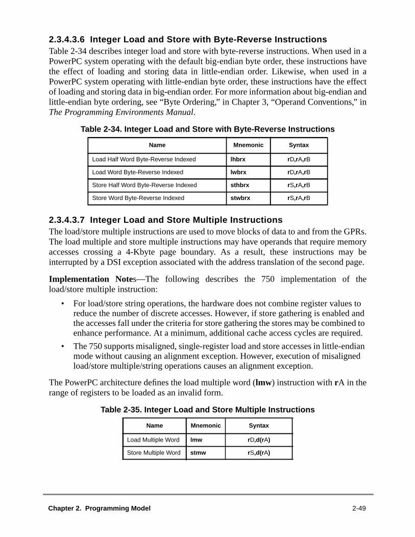
d in ahave
in aeffectand
,” in
PRs.moryay bepage.
he
es tod anded to
uired.
ndianned
2.3.4.3.6 Integer Load and Store with Byte-Reverse InstructionsTable 2-34 describes integer load and store with byte-reverse instructions. When usePowerPC system operating with the default big-endian byte order, these instructionsthe effect of loading and storing data in little-endian order. Likewise, when usedPowerPC system operating with little-endian byte order, these instructions have theof loading and storing data in big-endian order. For more information about big-endianlittle-endian byte ordering, see “Byte Ordering,” in Chapter 3, “Operand ConventionsThe Programming Environments Manual.
2.3.4.3.7 Integer Load and Store Multiple InstructionsThe load/store multiple instructions are used to move blocks of data to and from the GThe load multiple and store multiple instructions may have operands that require meaccesses crossing a 4-Kbyte page boundary. As a result, these instructions minterrupted by a DSI exception associated with the address translation of the second
Implementation Notes—The following describes the 750 implementation of tload/store multiple instruction:
• For load/store string operations, the hardware does not combine register valureduce the number of discrete accesses. However, if store gathering is enablethe accesses fall under the criteria for store gathering the stores may be combinenhance performance. At a minimum, additional cache access cycles are req
• The 750 supports misaligned, single-register load and store accesses in little-emode without causing an alignment exception. However, execution of misaligload/store multiple/string operations causes an alignment exception.
The PowerPC architecture defines the load multiple word (lmw) instruction withrA in therange of registers to be loaded as an invalid form.
Table 2-34. Integer Load and Store with Byte-Reverse Instructions
Name Mnemonic Syntax
Load Half Word Byte-Reverse Indexed lhbrx r D,rA,rB
Load Word Byte-Reverse Indexed lwbrx r D,rA,rB
Store Half Word Byte-Reverse Indexed sthbrx r S,rA,rB
Store Word Byte-Reverse Indexed stwbrx r S,rA,rB
Table 2-35. Integer Load and Store Multiple Instructions
Name Mnemonic Syntax
Load Multiple Word lmw r D,d(rA)
Store Multiple Word stmw r S,d(rA)
Chapter 2. Programming Model 2-49

ry tos canove
ctionsthan ae 2-36
of a
ned.
ringe type.gnedeption.lower
re
es tod anded to
uired.
ndianned
2.3.4.3.8 Integer Load and Store String InstructionsThe integer load and store string instructions allow movement of data from memoregisters or from registers to memory without concern for alignment. These instructionbe used for a short move between arbitrary memory locations or to initiate a long mbetween misaligned memory fields. However, in some implementations, these instruare likely to have greater latency and take longer to execute, perhaps much longer,sequence of individual load or store instructions that produce the same results. Tablsummarizes the integer load and store string instructions.
In other PowerPC implementations operating with little-endian byte order, executionload or string instruction invokes the alignment error handler; see “Byte Ordering,” inTheProgramming Environments Manual for more information.
Load string and store string instructions may involve operands that are not word-alig
As described in Section 4.5.6, “Alignment Exception (0x00600),” a misaligned stoperation suffers a performance penalty compared to an aligned operation of the samA non–word-aligned string operation that crosses a 4-Kbyte boundary, or a word-alistring operation that crosses a 256-Mbyte boundary always causes an alignment excA non–word-aligned string operation that crosses a double-word boundary is also sthan a word-aligned string operation.
Implementation Note—The following describes the 750 implementation of load/stostring instructions:
• For load/store string operations, the hardware does not combine register valureduce the number of discrete accesses. However, if store gathering is enablethe accesses fall under the criteria for store gathering the stores may be combinenhance performance. At a minimum, additional cache access cycles are req
• The 750 supports misaligned, single-register load and store accesses in little-emode without causing an alignment exception. However, execution of misaligload/store multiple/string operations cause an alignment exception.
Table 2-36. Integer Load and Store String Instructions
Name Mnemonic Syntax
Load String Word Immediate lswi r D,rA,NB
Load String Word Indexed lswx r D,rA,rB
Store String Word Immediate stswi r S,rA,NB
Store String Word Indexed stswx r S,rA,rB
2-50 IBM PowerPC 740 / PowerPC 750 RISC Microprocessor User’s Manual

egisterssinghe useption.
and-pointvertPR.
0] = therlier
ne
of them isint,tore
the
2.3.4.3.9 Floating-Point Load and Store Address GenerationFloating-point load and store operations generate effective addresses using the rindirect with immediate index addressing mode and register indirect with index addremode. Floating-point loads and stores are not supported for direct-store accesses. Tof floating-point loads and stores for direct-store access results in an alignment exce
There are two forms of the floating-point load instruction—single-precisiondouble-precision operand formats. Because the FPRs support only the floatingdouble-precision format, single-precision floating-point load instructions consingle-precision data to double-precision format before loading an operand into an F
Implementation Notes—The 750 treats exceptions as follows:
• The FPU can be run in two different modes—ignore exceptions mode (MSR[FEMSR[FE1] = 0) and precise mode (any other settings for MSR[FE0,FE1]). For750, ignore exceptions mode allows floating-point instructions to complete eaand thus may provide better performance than precise mode.
• The floating-point load and store indexed instructions (lfsx, lfsux, lfdx , lfdux , stfsx,stfsux, stfdx, stfdux) are invalid when the Rc bit is one. In the 750, executing oof these invalid instruction forms causes CR0 to be set to an undefined value.
The PowerPC architecture defines a load with update instruction withrA = 0 as an invalidform. Table 2-37 summarizes the floating-point load instructions.
2.3.4.3.10 Floating-Point Store InstructionsThis section describes floating-point store instructions. There are three basic formsstore instruction—single-precision, double-precision, and integer. The integer forsupported by the optionalstfiwx instruction. Because the FPRs support only floating-podouble-precision format for floating-point data, single-precision floating-point sinstructions convert double-precision data to single-precision format before storingoperands. Table 2-38 summarizes the floating-point store instructions.
Table 2-37. Floating-Point Load Instructions
Name Mnemonic Syntax
Load Floating-Point Single lfs fr D,d(rA)
Load Floating-Point Single Indexed lfsx fr D,rA,rB
Load Floating-Point Single with Update lfsu fr D,d(rA)
Load Floating-Point Single with Update Indexed lfsux fr D,rA,rB
Load Floating-Point Double lfd fr D,d(rA)
Load Floating-Point Double Indexed lfdx fr D,rA,rB
Load Floating-Point Double with Update lfdu fr D,d(rA)
Load Floating-Point Double with Update Indexed lfdux fr D,rA,rB
Chapter 2. Programming Model 2-51

howsn.
e
Some floating-point store instructions require conversions in the LSU. Table 2-39 sconversions the LSU makes when executing a Store Floating-Point Single instructio
Note: The FPRs are not initialized byHRESET, and they must be initialized with somvalid value after PORHRESET and before being stored.
Table 2-38. Floating-Point Store Instructions
Name Mnemonic Syntax
Store Floating-Point Single stfs fr S,d(rA)
Store Floating-Point Single Indexed stfsx fr S,r B
Store Floating-Point Single with Update stfsu fr S,d(rA)
Store Floating-Point Single with Update Indexed stfsux fr S,r B
Store Floating-Point Double stfd fr S,d(rA)
Store Floating-Point Double Indexed stfdx fr S,rB
Store Floating-Point Double with Update stfdu fr S,d(rA)
Store Floating-Point Double with Update Indexed stfdux fr S,r B
Store Floating-Point as Integer Word Indexed 1 stfiwx fr S,rB
Note: 1The stfiwx instruction is optional to the PowerPC architecture.
Table 2-39. Store Floating-Point Single Behavior
FPR Precision Data Type Action
Single Normalized Store
Single Denormalized Store
Single Zero, infinity, QNaN Store
Single SNaN Store
Double Normalized If(exp 896)then Denormalize and Storeelse
Store
Double Denormalized Store zero
Double Zero, infinity, QNaN Store
Double SNaN Store
2-52 IBM PowerPC 740 / PowerPC 750 RISC Microprocessor User’s Manual
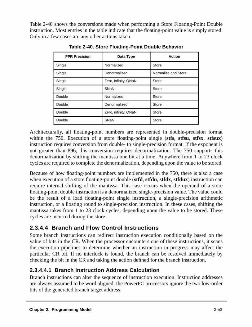
oublered.
rmat
nt iss thislockstored.
case
storeouldetic
g theThese
n thescanst theby
resses-order
Table 2-40 shows the conversions made when performing a Store Floating-Point Dinstruction. Most entries in the table indicate that the floating-point value is simply stoOnly in a few cases are any other actions taken.
Architecturally, all floating-point numbers are represented in double-precision fowithin the 750. Execution of a store floating-point single (stfs, stfsu, stfsx, stfsux)instruction requires conversion from double- to single-precision format. If the exponenot greater than 896, this conversion requires denormalization. The 750 supportdenormalization by shifting the mantissa one bit at a time. Anywhere from 1 to 23 ccycles are required to complete the denormalization, depending upon the value to be
Because of how floating-point numbers are implemented in the 750, there is also awhen execution of a store floating-point double (stfd, stfdu, stfdx, stfdux) instruction canrequire internal shifting of the mantissa. This case occurs when the operand of afloating-point double instruction is a denormalized single-precision value. The value cbe the result of a load floating-point single instruction, a single-precision arithminstruction, or a floating round to single-precision instruction. In these cases, shiftinmantissa takes from 1 to 23 clock cycles, depending upon the value to be stored.cycles are incurred during the store.
2.3.4.4 Branch and Flow Control InstructionsSome branch instructions can redirect instruction execution conditionally based ovalue of bits in the CR. When the processor encounters one of these instructions, itthe execution pipelines to determine whether an instruction in progress may affecparticular CR bit. If no interlock is found, the branch can be resolved immediatelychecking the bit in the CR and taking the action defined for the branch instruction.
2.3.4.4.1 Branch Instruction Address CalculationBranch instructions can alter the sequence of instruction execution. Instruction addare always assumed to be word aligned; the PowerPC processors ignore the two lowbits of the generated branch target address.
Table 2-40. Store Floating-Point Double Behavior
FPR Precision Data Type Action
Single Normalized Store
Single Denormalized Normalize and Store
Single Zero, infinity, QNaN Store
Single SNaN Store
Double Normalized Store
Double Denormalized Store
Double Zero, infinity, QNaN Store
Double SNaN Store
Chapter 2. Programming Model 2-53

wing
sen thect ortively. This
plifyvidedshift,
tion
Branch instructions compute the EA of the next instruction address using the folloaddressing modes:
• Branch relative• Branch conditional to relative address• Branch to absolute address• Branch conditional to absolute address• Branch conditional to link register• Branch conditional to count register
Note that in the 750, all branch instructions (b, ba, bl, bla, bc, bca, bcl, bcla, bclr, bclrl ,bcctr, bcctrl ) and condition register logical instructions (crand, cror, crxor, crnand,crnor, crandc, creqv, crorc, and mcrf ) are executed by the BPU. Some of theinstructions can redirect instruction execution conditionally based on the value of bits iCR. Whenever the CR bits resolve, the branch direction is either marked as corremispredicted. Correcting a mispredicted branch requires that the 750 flush speculaexecuted instructions and restore the machine state to immediately after the branchcorrection can be done immediately upon resolution of the condition registers bits.
2.3.4.4.2 Branch InstructionsTable 2-41 lists the branch instructions provided by the PowerPC processors. To simassembly language programming, a set of simplified mnemonics and symbols is profor the most frequently used forms of branch conditional, compare, trap, rotate andand certain other instructions. See Appendix F, “Simplified Mnemonics,” inTheProgramming Environments Manualfor a list of simplified mnemonic examples.
2.3.4.4.3 Condition Register Logical InstructionsCondition register logical instructions, shown in Table 2-42, and the Move CondiRegister Field (mcrf ) instruction are also defined as flow control instructions.
Table 2-41. Branch Instructions
Name Mnemonic Syntax
Branch b (ba bl bla) target_addr
Branch Conditional bc (bca bcl bcla) BO,BI,target_addr
Branch Conditional to Link Register bclr (bclrl) BO,BI
Branch Conditional to Count Register bcctr (bcctrl) BO,BI
Table 2-42. Condition Register Logical Instructions
Name Mnemonic Syntax
Condition Register AND crand crb D,crb A,crb B
Condition Register OR cror crb D,crb A,crb B
Condition Register XOR crxor crb D,crb A,crb B
2-54 IBM PowerPC 740 / PowerPC 750 RISC Microprocessor User’s Manual

erPC
et oftype
ptionally.
rm aEA,”
r more
gister. See
Note that if the LR update option is enabled for any of these instructions, the Powarchitecture defines these forms of the instructions as invalid.
2.3.4.4.4 Trap InstructionsThe trap instructions shown in Table 2-43 are provided to test for a specified sconditions. If any of the conditions tested by a trap instruction are met, the system trapprogram exception is taken. For more information, see Section 4.5.7, “Program Exce(0x00700).” If the tested conditions are not met, instruction execution continues norm
See Appendix F, “Simplified Mnemonics,” inThe Programming Environments Manualfora complete set of simplified mnemonics.
2.3.4.5 System Linkage Instruction—UISAThe System Call (sc) instruction permits a program to call on the system to perfoservice; see Table 2-44. See also Section 2.3.6.1, “System Linkage Instructions—Ofor additional information.
Executing this instruction causes the system call exception handler to be evoked. Foinformation, see Section 4.5.10, “System Call Exception (0x00C00).”
2.3.4.6 Processor Control Instructions—UISAProcessor control instructions are used to read from and write to the condition re(CR), machine state register (MSR), and special-purpose registers (SPRs)
Condition Register NAND crnand crb D,crb A,crb B
Condition Register NOR crnor crb D,crb A,crb B
Condition Register Equivalent creqv crb D,crb A, crb B
Condition Register AND with Complement crandc crb D,crb A, crb B
Condition Register OR with Complement crorc crb D,crb A, crb B
Move Condition Register Field mcrf crf D,crf S
Table 2-43. Trap Instructions
Name Mnemonic Syntax
Trap Word Immediate twi TO,rA,SIMM
Trap Word tw TO,rA,rB
Table 2-44. System Linkage Instruction—UISA
Name Mnemonic Syntax
System Call sc —
Table 2-42. Condition Register Logical Instructions (Continued)
Name Mnemonic Syntax
Chapter 2. Programming Model 2-55

the
ister.
ions
gister
Section 2.3.5.1, “Processor Control Instructions—VEA,” for themftb instruction andSection 2.3.6.2, “Processor Control Instructions—OEA,” for information aboutinstructions used for reading from and writing to the MSR and SPRs.
2.3.4.6.1 Move to/from Condition Register InstructionsTable 2-45 summarizes the instructions for reading from or writing to the condition reg
Implementation Note—The PowerPC architecture indicates that in some implementatthe Move to Condition Register Fields (mtcrf ) instruction may perform more slowly whenonly a portion of the fields are updated as opposed to all of the fields. The condition reaccess latency for the 750 is the same in both cases.
2.3.4.6.2 Move to/from Special-Purpose Register Instructions (UISA)Table 2-46 lists themtspr andmfspr instructions.
Table 2-47 lists the SPR numbers for both user- and supervisor-level accesses.
Table 2-45. Move to/from Condition Register Instructions
Name Mnemonic Syntax
Move to Condition Register Fields mtcrf CRM,rS
Move to Condition Register from XER mcrxr crf D
Move from Condition Register mfcr r D
Table 2-46. Move to/from Special-Purpose Register Instructions (UISA)
Name Mnemonic Syntax
Move to Special-Purpose Register mtspr SPR,rS
Move from Special-Purpose Register mfspr r D,SPR
Table 2-47. PowerPC Encodings
Register NameSPR
1
Access mfspr/mtsprDecimal spr[5–9] spr[0–4]
CTR 9 00000 01001 User (UISA) Both
DABR 1013 11111 10101 Supervisor (OEA) Both
DAR 19 00000 10011 Supervisor (OEA) Both
DBAT0L 537 10000 11001 Supervisor (OEA) Both
DBAT0U 536 10000 11000 Supervisor (OEA) Both
DBAT1L 539 10000 11011 Supervisor (OEA) Both
DBAT1U 538 10000 11010 Supervisor (OEA) Both
DBAT2L 541 10000 11101 Supervisor (OEA) Both
2-56 IBM PowerPC 740 / PowerPC 750 RISC Microprocessor User’s Manual

DBAT2U 540 10000 11100 Supervisor (OEA) Both
DBAT3L 543 10000 11111 Supervisor (OEA) Both
DBAT3U 542 10000 11110 Supervisor (OEA) Both
DEC 22 00000 10110 Supervisor (OEA) Both
DSISR 18 00000 10010 Supervisor (OEA) Both
EAR 282 01000 11010 Supervisor (OEA) Both
IBAT0L 529 10000 10001 Supervisor (OEA) Both
IBAT0U 528 10000 10000 Supervisor (OEA) Both
IBAT1L 531 10000 10011 Supervisor (OEA) Both
IBAT1U 530 10000 10010 Supervisor (OEA) Both
IBAT2L 533 10000 10101 Supervisor (OEA) Both
IBAT2U 532 10000 10100 Supervisor (OEA) Both
IBAT3L 535 10000 10111 Supervisor (OEA) Both
IBAT3U 534 10000 10110 Supervisor (OEA) Both
LR 8 00000 01000 User (UISA) Both
PVR 287 01000 11111 Supervisor (OEA) mfspr
SDR1 25 00000 11001 Supervisor (OEA) Both
SPRG0 272 01000 10000 Supervisor (OEA) Both
SPRG1 273 01000 10001 Supervisor (OEA) Both
SPRG2 274 01000 10010 Supervisor (OEA) Both
SPRG3 275 01000 10011 Supervisor (OEA) Both
SRR0 26 00000 11010 Supervisor (OEA) Both
SRR1 27 00000 11011 Supervisor (OEA) Both
TBL 2 268 01000 01100 Supervisor (OEA) mtspr
284 01000 11100 Supervisor (OEA) mtspr
TBU 2 269 01000 01101 Supervisor (OEA) mtspr
285 01000 11101 Supervisor (OEA) mtspr
Table 2-47. PowerPC Encodings (Continued)
Register NameSPR
1
Access mfspr/mtsprDecimal spr[5–9] spr[0–4]
Chapter 2. Programming Model 2-57

Encodings for the 750-specific SPRs are listed in Table 2-48.
XER 1 00000 00001 User (UISA) Both
Notes :1 The order of the two 5-bit halves of the SPR number is reversed compared with actual
instruction coding. For mtspr and mfspr instructions, the SPR number coded in assemblylanguage does not appear directly as a 10-bit binary number in the instruction. The numbercoded is split into two 5-bit halves that are reversed in the instruction, with the high-order fivebits appearing in bits 16–20 of the instruction and the low-order five bits in bits 11–15.
2 The TB registers are referred to as TBRs rather than SPRs and can be written to using themtspr instruction in supervisor mode and the TBR numbers here. The TB registers can be readin user mode using either the mftb or mtspr instruction and specifying TBR 268 for TBL andSPR 269 for TBU.
Table 2-48. SPR Encodings for PowerPC 750-Defined Registers (mfspr)
RegisterName
SPR1
Access mfspr/mtsprDecimal spr[5–9] spr[0–4]
DABR 1013 11111 10101 User Both
HID0 1008 11111 10000 Supervisor Both
HID1 1009 11111 10001 Supervisor Both
IABR 1010 11111 10010 Supervisor Both
ICTC 1019 11111 11011 Supervisor Both
L2CR 1017 11111 11001 Supervisor Both
MMCR0 952 11101 11000 Supervisor Both
MMCR1 956 11101 11100 Supervisor Both
PMC1 953 11101 11001 Supervisor Both
PMC2 954 11101 11010 Supervisor Both
PMC3 957 11101 11101 Supervisor Both
PMC4 958 11101 11110 Supervisor Both
SIA 955 11101 11011 Supervisor Both
THRM1 1020 11111 11100 Supervisor Both
THRM2 1021 11111 11101 Supervisor Both
THRM3 1022 11111 11110 Supervisor Both
UMMCR0 936 11101 01000 User mfspr
Table 2-47. PowerPC Encodings (Continued)
Register NameSPR
1
Access mfspr/mtsprDecimal spr[5–9] spr[0–4]
2-58 IBM PowerPC 740 / PowerPC 750 RISC Microprocessor User’s Manual

areationstructionabout
2.3.4.7 Memory Synchronization Instructions—UISAMemory synchronization instructions control the order in which memory operationscompleted with respect to asynchronous events, and the order in which memory operare seen by other processors or memory access mechanisms. See Chapter 3, “Insand Data Cache Operation,” for additional information about these instructions andrelated aspects of memory synchronization. See Table 2-49 for a summary.
UMMCR1 940 11101 01100 User mfspr
UPMC1 937 11101 01001 User mfspr
UPMC2 938 11101 01010 User mfspr
UPMC3 941 11101 01101 User mfspr
UPMC4 942 11101 01110 User mfspr
USIA 939 11101 01011 User mfspr
Note :1Note that the order of the two 5-bit halves of the SPR number is reversed compared with actualinstruction coding.
For mtspr and mfspr instructions, the SPR number coded in assembly language does notappear directly as a 10-bit binary number in the instruction. The number coded is split into two5-bit halves that are reversed in the instruction, with the high-order 5 bits appearing in bits16–20 of the instruction and the low-order 5 bits in bits 11–15.
Table 2-49. Memory Synchronization Instructions—UISA
Name Mnemonic Syntax Implementation Notes
Load Wordand ReserveIndexed
lwarx r D,rA,rB Programmers can use lwarx with stwcx. to emulate common semaphoreoperations such as test and set, compare and swap, exchange memory, andfetch and add. Both instructions must use the same EA. Reservationgranularity is implementation-dependent. The 750 makes reservations onbehalf of aligned 32-byte sections of the memory address space. If the W bit isset, executing lwarx and stwcx. to a page marked write-through does notcause a DSI exception, but DSI exceptions can result for other reasons. If thelocation is not word-aligned, an alignment exception occurs.The stwcx. instruction is the only load/store instruction with a valid form if Rc isset. If Rc is zero, executing stwcx. sets CR0 to an undefined value. In general,stwcx. always causes a transaction on the external bus and thus operates withslightly worse performance characteristics than normal store operations.
Store WordConditionalIndexed
stwcx. r S,rA,rB
Table 2-48. SPR Encodings for PowerPC 750-Defined Registers (mfspr) (Continued)
RegisterName
SPR1
Access mfspr/mtsprDecimal spr[5–9] spr[0–4]
Chapter 2. Programming Model 2-59

dwarens toe been
nal
tions.
f thes of thessues.sarily
EAasetion.
System designs with an L2 cache should take special care to recognize the harsignaling caused by a SYNC bus operation and perform the appropriate actioguarantee that memory references that may be queued internally to the L2 cache havperformed globally.
See 2.3.5.2, “Memory Synchronization Instructions—VEA,” for details about additiomemory synchronization (eieio andisync) instructions.
In the PowerPC architecture, the Rc bit must be zero for most load and store instrucIf Rc is set, the instruction form is invalid forsync and lwarx instructions. If the 750encounters one of these invalid instruction forms, it sets CR0 to an undefined value.
2.3.5 PowerPC VEA InstructionsThe PowerPC virtual environment architecture (VEA) describes the semantics omemory model that can be assumed by software processes, and includes descriptioncache model, cache control instructions, address aliasing, and other related iImplementations that conform to the VEA also adhere to the UISA, but may not necesadhere to the OEA.
This section describes additional instructions that are provided by the VEA.
2.3.5.1 Processor Control Instructions—VEAIn addition to the move to condition register instructions (specified by the UISA), the Vdefines themftb instruction (user-level instruction) for reading the contents of the time bregister; see Chapter 3, “Instruction and Data Cache Operation,” for more informaTable 2-50 shows themftb instruction.
Synchronize sync — Because it delays subsequent instructions until all previous instructionscomplete to where they cannot cause an exception, sync is a barrier againststore gathering. Additionally, all load/store cache/bus activities initiated by priorinstructions are completed. Touch load operations (dcbt , dcbtst ) mustcomplete address translation, but need not complete on the bus. If HID0[ABE]= 1, sync completes after a successful broadcast.The latency of sync depends on the processor state when it is dispatched andon various system-level situations. Therefore, frequent use of sync maydegrade performance.
Table 2-50. Move from Time Base Instruction
Name Mnemonic Syntax
Move from Time Base mftb r D, TBR
Table 2-49. Memory Synchronization Instructions—UISA (Continued)
Name Mnemonic Syntax Implementation Notes
2-60 IBM PowerPC 740 / PowerPC 750 RISC Microprocessor User’s Manual
ed. See
ase
ed,
ores
e
use of
ndB
bus
areationstructionelated
e
rsof this
Simplified mnemonics are provided for themftb instruction so it can be coded with thTBR name as part of the mnemonic rather than requiring it to be coded as an operanAppendix F, “Simplified Mnemonics,” inThe Programming Environments Manualforsimplified mnemonic examples and for simplified mnemonics for Move from Time B(mftb ) and Move from Time Base Upper (mftbu ), which are variants of themftbinstruction rather than ofmfspr. Themftb instruction serves as both a basic and simplifimnemonic. Assemblers recognize anmftb mnemonic with two operands as the basic formand anmftb mnemonic with one operand as the simplified form. Note that the 750 ignthe extended opcode differences betweenmftb andmfspr by ignoring bit 25 and treatingboth instructions identically.
Implementation Notes—The following information is useful with respect to using thtime base implementation in the 750:
• The 750 allows user-mode read access to the time base counter through the the Move from Time Base (mftb ) and the Move from Time Base Upper (mftbu )instructions. As a 32-bit PowerPC implementation, the 750 can access TBU aTBL only separately, whereas 64-bit implementations can access the entire Tregister at once.
• The time base counter is clocked at a frequency that is one-fourth that of the clock. Counting is enabled by assertion of the time base enable (TBE) input signal.
2.3.5.2 Memory Synchronization Instructions—VEAMemory synchronization instructions control the order in which memory operationscompleted with respect to asynchronous events, and the order in which memory operare seen by other processors or memory access mechanisms. See Chapter 3, “Insand Data Cache Operation,” for more information about these instructions and about raspects of memory synchronization.
In addition to thesync instruction (specified by UISA), the VEA defines the EnforcIn-Order Execution of I/O (eieio) and Instruction Synchronize (isync) instructions. Thenumber of cycles required to complete aneieio instruction depends on system parameteand on the processor's state when the instruction is issued. As a result, frequent useinstruction may degrade performance slightly.
Chapter 2. Programming Model 2-61

VEA.outbuffer
-chipn,” forations
tionsotherystem
t
Table 2-51 describes the memory synchronization instructions defined by the VEA.
2.3.5.3 Memory Control Instructions—VEAMemory control instructions can be classified as follows:
• Cache management instructions (user-level and supervisor-level)• Segment register manipulation instructions (OEA)• Translation lookaside buffer management instructions (OEA)
This section describes the user-level cache management instructions defined by theSee Section 2.3.6.3, “Memory Control Instructions—OEA,” for information absupervisor-level cache, segment register manipulation, and translation lookasidemanagement instructions.
2.3.5.3.1 User-Level Cache Instructions—VEAThe instructions summarized in this section help user-level programs manage oncaches if they are implemented. See Chapter 3, “Instruction and Data Cache Operatiomore information about cache topics. The following sections describe how these operare treated with respect to the 750’s cache.
As with other memory-related instructions, the effects of cache management instrucon memory are weakly-ordered. If the programmer must ensure that cache orinstructions have been performed with respect to all other processors and smechanisms, async instruction must be placed after those instructions.
Note that the 750 interprets cache control instructions (icbi, dcbi, dcbf, dcbz, anddcbst)as if they pertain only to the local L1 and L2 cache. Adcbz(with M set) is always broadcason the 60x bus. Thedcbi, dcbf, anddcbst operations are broadcast if HID0[ABE] is set.
Table 2-51. Memory Synchronization Instructions—VEA
Name Mnemonic Syntax Implementation Notes
EnforceIn-OrderExecution ofI/O
eieio — The eieio instruction is dispatched to the LSU and executes after all previouscache-inhibited or write-through accesses are performed; all subsequentinstructions that generate such accesses execute after eieio . If HID0[ABE] = 1 anEIEIO operation is broadcast on the external bus to enforce ordering in theexternal memory system. The eieio operation bypasses the L2 cache and isforwarded to the bus unit. If HID0[ABE] = 0, the operation is not broadcast.Because the 750 does not reorder noncacheable accesses, eieio is not neededto force ordering. However, if store gathering is enabled and an eieio is detectedin a store queue, stores are not gathered. If HID0[ABE] = 1, broadcasting eieioprevents external devices, such as a bus bridge chip, from gathering stores.
InstructionSynchronize
isync — The isync instruction is refetch serializing; that is, it causes the 750 to purge itsinstruction queue and wait for all prior instructions to complete before refetchingthe next instruction, which is not executed until all previous instructions completeto the point where they cannot cause an exception. The isync instruction doesnot wait for all pending stores in the store queue to complete. Any instructionafter an isync sees all effects of prior instructions.
2-62 IBM PowerPC 740 / PowerPC 750 RISC Microprocessor User’s Manual

nlycheche
ntrol
these
The 750 never broadcasts anicbi. Of the broadcast cache operations, the 750 snoops odcbz, regardless of the HID0[ABE] setting. Any bus activity caused by other cainstructions results directly from performing the operation on the 750 cache. All cacontrol instructions to T = 1 space are no-ops. For information how cache coinstructions affect the L2, see Chapter 9, “L2 Cache Interface Operation.”
Table 2-52 summarizes the cache instructions defined by the VEA. Note thatinstructions are accessible to user-level programs.
Table 2-52. User-Level Cache Instructions
Name Mnemonic Syntax Implementation Notes
Data Cache BlockTouch 1
dcbt r A,rB The VEA defines this instruction to allow for potential system performanceenhancements through the use of software-initiated prefetch hints.Implementations are not required to take any action based on execution ofthis instruction, but they may prefetch the cache block corresponding tothe EA into their cache. When dcbt executes, the 750 checks forprotection violations (as for a load instruction). This instruction is treatedas a no-op for the following cases:• A valid translation is not found either in BAT or TLB• The access causes a protection violation.• The page is mapped cache-inhibited, G = 1 (guarded), or T = 1.• The cache is locked or disabled• HID0[NOOPTI] = 1Otherwise, if no data is in the cache location, the 750 requests a cacheline fill (with intent to modify). Data brought into the cache is validated as ifit were a load instruction. The memory reference of a dcbt sets thereference bit.
Data Cache BlockTouch for Store 1
dcbtst r A,rB This instruction behaves like dcbt .
Data Cache BlockSet to Zero
dcbz r A,rB The EA is computed, translated, and checked for protection violations. Forcache hits, four beats of zeros are written to the cache block and the tag ismarked M. For cache misses with the replacement block marked E, thezero line fill is performed and the cache block is marked M. However, if thereplacement block is marked M, the contents are written back to memoryfirst. The instruction executes regardless of whether the cache is locked; ifthe cache is disabled, an alignment exception occurs. If M = 1 (coherencyenforced), the address is broadcast to the bus before the zero line fill.The exception priorities (from highest to lowest) are as follows:1 Cache disabled—Alignment exception2 Page marked write-through or cache Inhibited—Alignment exception3 BAT protection violation—DSI exception4 TLB protection violation—DSI exceptiondcbz is the only cache instruction that broadcasts even if HID0[ABE] = 0.
Chapter 2. Programming Model 2-63
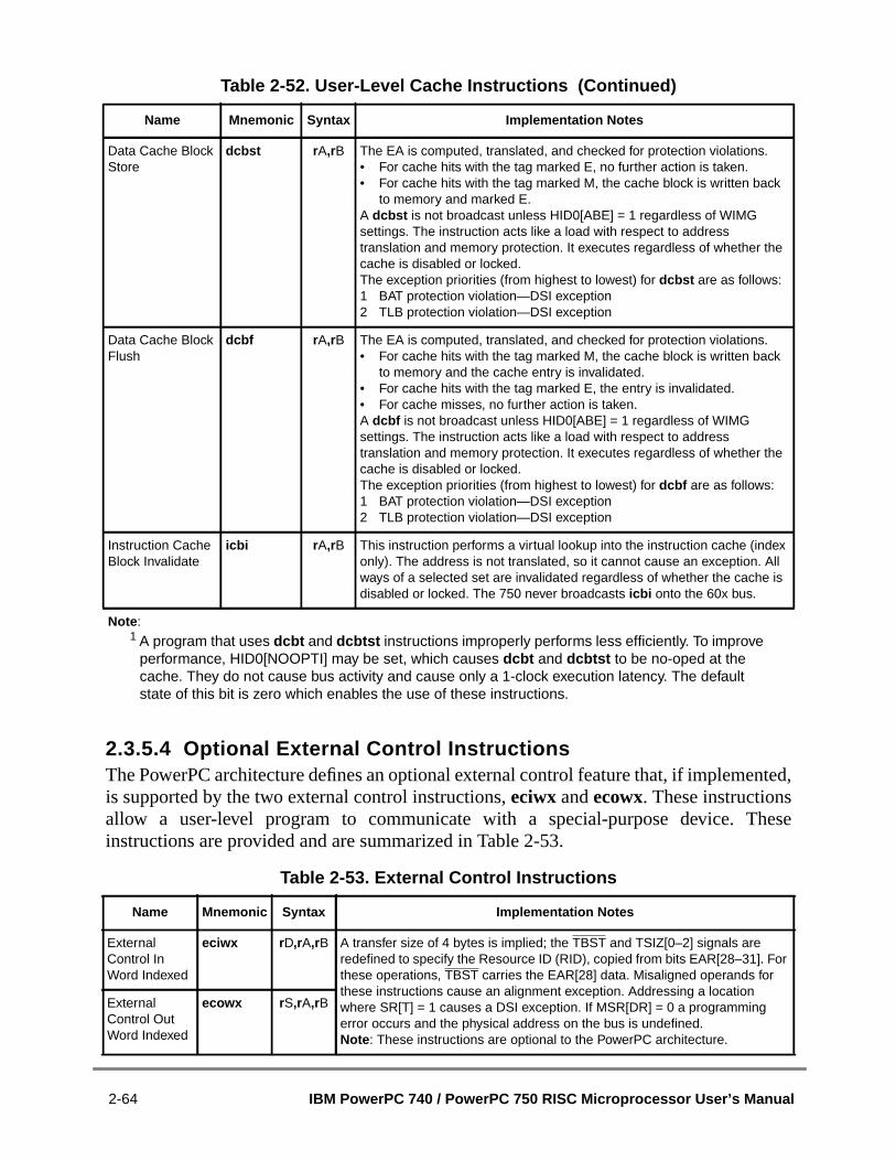
nted,
hese
2.3.5.4 Optional External Control InstructionsThe PowerPC architecture defines an optional external control feature that, if implemeis supported by the two external control instructions,eciwxandecowx. These instructionsallow a user-level program to communicate with a special-purpose device. Tinstructions are provided and are summarized in Table 2-53.
Data Cache BlockStore
dcbst r A,rB The EA is computed, translated, and checked for protection violations.• For cache hits with the tag marked E, no further action is taken.• For cache hits with the tag marked M, the cache block is written back
to memory and marked E.A dcbst is not broadcast unless HID0[ABE] = 1 regardless of WIMGsettings. The instruction acts like a load with respect to addresstranslation and memory protection. It executes regardless of whether thecache is disabled or locked.The exception priorities (from highest to lowest) for dcbst are as follows:1 BAT protection violation—DSI exception2 TLB protection violation—DSI exception
Data Cache BlockFlush
dcbf r A,rB The EA is computed, translated, and checked for protection violations.• For cache hits with the tag marked M, the cache block is written back
to memory and the cache entry is invalidated.• For cache hits with the tag marked E, the entry is invalidated.• For cache misses, no further action is taken.A dcbf is not broadcast unless HID0[ABE] = 1 regardless of WIMGsettings. The instruction acts like a load with respect to addresstranslation and memory protection. It executes regardless of whether thecache is disabled or locked.The exception priorities (from highest to lowest) for dcbf are as follows:1 BAT protection violation—DSI exception2 TLB protection violation—DSI exception
Instruction CacheBlock Invalidate
icbi r A,rB This instruction performs a virtual lookup into the instruction cache (indexonly). The address is not translated, so it cannot cause an exception. Allways of a selected set are invalidated regardless of whether the cache isdisabled or locked. The 750 never broadcasts icbi onto the 60x bus.
Note :1 A program that uses dcbt and dcbtst instructions improperly performs less efficiently. To improve
performance, HID0[NOOPTI] may be set, which causes dcbt and dcbtst to be no-oped at thecache. They do not cause bus activity and cause only a 1-clock execution latency. The defaultstate of this bit is zero which enables the use of these instructions.
Table 2-53. External Control Instructions
Name Mnemonic Syntax Implementation Notes
ExternalControl InWord Indexed
eciwx r D,rA,rB A transfer size of 4 bytes is implied; the TBST and TSIZ[0–2] signals areredefined to specify the Resource ID (RID), copied from bits EAR[28–31]. Forthese operations, TBST carries the EAR[28] data. Misaligned operands forthese instructions cause an alignment exception. Addressing a locationwhere SR[T] = 1 causes a DSI exception. If MSR[DR] = 0 a programmingerror occurs and the physical address on the bus is undefined.Note : These instructions are optional to the PowerPC architecture.
ExternalControl OutWord Indexed
ecowx r S,rA,rB
Table 2-52. User-Level Cache Instructions (Continued)
Name Mnemonic Syntax Implementation Notes
2-64 IBM PowerPC 740 / PowerPC 750 RISC Microprocessor User’s Manual

ativeusedand thatsignalsrce IDs
ween.”
f theodel.
This
veles the
nd the
Theeciwx/ecowxinstructions let a system designer map special devices in an alternway. The MMU translation of the EA is not used to select the special device, as it isin most instructions such as loads and stores. Rather, it is used as an address operis passed to the device over the address bus. Four other signals (the burst and sizeon the 60x bus) are used to select the device; these four signals output the 4-bit resou(RID) field located in the EAR. Theeciwx instruction also loads a word from the data buthat is output by the special device. For more information about the relationship betthese instructions and the system interface, refer to Chapter 7, “Signal Descriptions
2.3.6 PowerPC OEA InstructionsThe PowerPC operating environment architecture (OEA) includes the structure omemory management model, supervisor-level registers, and the exception mImplementations that conform to the OEA also adhere to the UISA and the VEA.section describes the instructions provided by the OEA.
2.3.6.1 System Linkage Instructions—OEAThis section describes the system linkage instructions (see Table 2-54). The user-lescinstruction lets a user program call on the system to perform a service and causprocessor to take a system call exception. The supervisor-levelrfi instruction is used forreturning from an exception handler.
2.3.6.2 Processor Control Instructions—OEAThis section describes the processor control instructions used to access the MSR aSPRs. Table 2-55 lists instructions for accessing the MSR.
Table 2-54. System Linkage Instructions—OEA
Name Mnemonic Syntax Implementation Notes
System Call sc — The sc instruction is context-synchronizing.
Return fromInterrupt
rfi — The rfi instruction is context-synchronizing. For the 750, this means the rfiinstruction works its way to the final stage of the execution pipeline,updates architected registers, and redirects the instruction flow.
Table 2-55. Move to/from Machine State Register Instructions
Name Mnemonic Syntax
Move to Machine State Register mtmsr r S
Move from Machine State Register mfmsr r D
Chapter 2. Programming Model 2-65

l
s fors are
ntion
.5.3,ns.
thatctive
The OEA defines encodings ofmtspr and mfspr to provide access to supervisor-leveregisters. The instructions are listed in Table 2-56.
Encodings for the architecture-defined SPRs are listed in Table 2-47. Encoding750-specific, supervisor-level SPRs are listed in Table 2-48. Simplified mnemonicprovided for mtspr and mfspr in Appendix F, “Simplified Mnemonics,” inTheProgramming Environments Manual. For a discussion of context synchronizatiorequirements when altering certain SPRs, refer to Appendix E, “SynchronizaProgramming Examples,” inThe Programming Environments Manual.
2.3.6.3 Memory Control Instructions—OEAMemory control instructions include the following:
• Cache management instructions (supervisor-level and user-level)• Segment register manipulation instructions• Translation lookaside buffer management instructions
This section describes supervisor-level memory control instructions. Section 2.3“Memory Control Instructions—VEA,” describes user-level memory control instructio
2.3.6.3.1 Supervisor-Level Cache Management Instruction—(OEA)Table 2-57 lists the only supervisor-level cache management instruction.
See Section 2.3.5.3.1, “User-Level Cache Instructions—VEA,” for cache instructionsprovide user-level programs the ability to manage the on-chip caches. If the effeaddress references a direct-store segment, the instruction is treated as a no-op.
Table 2-56. Move to/from Special-Purpose Register Instructions (OEA)
Name Mnemonic Syntax
Move to Special-Purpose Register mtspr SPR,rS
Move from Special-Purpose Register mfspr r D,SPR
Table 2-57. Supervisor-Level Cache Management Instruction
Name Mnemonic Syntax Implementation Notes
DataCacheBlockInvalidate
dcbi r A,rB The EA is computed, translated, and checked for protection violations. For cachehits, the cache block is marked I regardless of whether it was marked E or M. Adcbi is not broadcast unless HID0[ABE] = 1, regardless of WIMG settings. Theinstruction acts like a store with respect to address translation and memoryprotection. It executes regardless of whether the cache is disabled or locked.The exception priorities (from highest to lowest) for dcbi are as follows:1 BAT protection violation—DSI exception2 TLB protection violation—DSI exception
2-66 IBM PowerPC 740 / PowerPC 750 RISC Microprocessor User’s Manual

2-bit] andand
ions
d pageddressegment
ons.
entedB
ute
2.3.6.3.2 Segment Register Manipulation Instructions (OEA)The instructions listed in Table 2-58 provide access to the segment registers for 3implementations. These instructions operate completely independently of the MSR[IRMSR[DR] bit settings. Refer to “Synchronization Requirements for Special Registersfor Lookaside Buffers,” in Chapter 2, “PowerPC Register Set,” ofThe ProgrammingEnvironments Manualfor serialization requirements and other recommended precautto observe when manipulating the segment registers.
2.3.6.3.3 Translation Lookaside Buffer Management Instructions—(OEA)The address translation mechanism is defined in terms of the segment descriptors antable entries (PTEs) PowerPC processors use to locate the logical-to-physical amapping for a particular access. These segment descriptors and PTEs reside in sregisters and page tables in memory, respectively.
See Chapter 7, “Memory Management,” for more information about TLB operatiTable 2-59 summarizes the operation of the TLB instructions in the 750.
Implementation Note—The tlbia instruction is optional for an implementation if itseffects can be achieved through some other mechanism. Therefore, it is not implemon the 750. As described above,tlbie can be used to invalidate a particular index of the TLbased on EA[14–19]—a sequence of 64tlbie instructions followed by atlbsync instructioninvalidates all the TLB structures (for EA[14–19] = 0, 1, 2,..., 63). Attempting to exectlbia causes an illegal instruction program exception.
Table 2-58. Segment Register Manipulation Instructions
Name Mnemonic Syntax Implementation Notes
Move to Segment Register mtsr SR,rS —
Move to Segment Register Indirect mtsrin r S,rB —
Move from Segment Register mfsr r D,SR The shadow SRs in the instruction MMU can be readby setting HID0[RISEG] before executing mfsr .
Move from Segment Register Indirect mfsrin r D,rB —
Table 2-59. Translation Lookaside Buffer Management Instruction
Name Mnemonic Syntax Implementation Notes
TLBInvalidateEntry
tlbie r B Invalidates both ways in both instruction and data TLB entries at the indexprovided by EA[14–19]. It executes regardless of the MSR[DR] and MSR[IR]settings.To invalidate all entries in both TLBs, the programmer should issue 64tlbie instructions that each successively increment this field.
TLBSynchronize
tlbsync — On the 750, the only function tlbsync serves is to wait for the TLBISYNC signalto go inactive.
Chapter 2. Programming Model 2-67

areould
someter, andfor thein this
,” in
The presence and exact semantics of the TLB management instructionsimplementation-dependent. To minimize compatibility problems, system software shincorporate uses of these instructions into subroutines.
2.3.7 Recommended Simplified MnemonicsTo simplify assembly language coding, a set of alternative mnemonics is provided forfrequently used operations (such as no-op, load immediate, load address, move regiscomplement register). Programs written to be portable across the various assemblersPowerPC architecture should not assume the existence of mnemonics not describeddocument.
For a complete list of simplified mnemonics, see Appendix F, “Simplified MnemonicsThe Programming Environments Manual.
2-68 IBM PowerPC 740 / PowerPC 750 RISC Microprocessor User’s Manual

ciativeess ton andcache
), the
ningdevicesasters
ture).
rithm
ag is
is the line.
tates:
two
Chapter 3Instruction and Data Cache Operation10
The PowerPC 750 microprocessor contains separate 32-Kbyte, eight-way set assoinstruction and data caches to allow the execution units and registers rapid accinstructions and data. This chapter describes the organization of the on-chip instructiodata caches, the MEI cache coherency protocol, cache control instructions, variousoperations, and the interaction between the caches, the load/store unit (LSUinstruction unit, and the bus interface unit (BIU).
Note that in this chapter, the term ‘multiprocessor’ is used in the context of maintaicache coherency. These multiprocessor devices could be actual processors or otherthat can access system memory, maintain their own caches, and function as bus mrequiring cache coherency.
The 750 cache implementation has the following characteristics:
• There are two separate 32-Kbyte instruction and data caches (Harvard architec
• Both instruction and data caches are eight-way set associative.
• The caches implement a pseudo least-recently-used (PLRU) replacement algowithin each set.
• The cache directories are physically addressed. The physical (real) address tstored in the cache directory.
• Both the instruction and data caches have 32-byte cache blocks. A cache blockblock of memory that a coherency state describes, also referred to as a cache
• Two coherency state bits for each data cache block allow encoding for three s
— Modified (Exclusive) (M)
— Exclusive (Unmodified) (E)
— Invalid (I)
• A single coherency state bit for each instruction cache block allows encoding forpossible states:
— Invalid (INV)
— Valid (VAL)
Chapter 3. Instruction and Data Cache Operation 3-1

ister
opingncy ofribed
burstis
izing
ss toceiveses thelogic,ue, and
• Each cache can be invalidated or locked by setting the appropriate bits in thehardware implementation-dependent register 0 (HID0), a special-purpose reg(SPR) specific to the 750.
The 750 supports a fully-coherent 4-Gbyte physical memory address space. Bus snois used to drive the MEI three-state cache coherency protocol that ensures the cohereglobal memory with respect to the processor’s data cache. The MEI protocol is descin Section 3.3.2, “MEI Protocol.”
On a cache miss, the 750’s cache blocks are filled in four beats of 64 bits each. Thefill is performed as a critical-double-word-first operation; the critical double wordsimultaneously written to the cache and forwarded to the requesting unit, thus minimstalls due to cache fill latency.
The instruction and data caches are integrated into the 750 as shown in Figure 3-1.
Figure 3-1. Cache Integration
Both caches are tightly coupled to the 750’s bus interface unit to allow efficient accethe system memory controller and other bus masters. The bus interface unit rerequests for bus operations from the instruction and data caches, and executoperations per the 60x bus protocol. The BIU provides address queues, prioritizingand bus control logic. The BIU captures snoop addresses for data cache, address quememory reservation (lwarx andstwcx. instruction) operations.
Instruction UnitLoad/Store Unit
Cache Tags
(LSU)
Instructions (0–127)
Instructions (0–63)
I-Cache32-Kbyte
8-Way Set Associative
Cache Logic
EA (20–26)
PA (0–19)
PA (0–31)
Cache Tags
Cache Logic
D-Cache
32-Kbyte8-Way Set Associative
Data (0–63)
Data (0–63)
EA: Effective AddressPA: Physical Address
MMU/L2 BIU (750 only)/60x BIU
3-2 IBM PowerPC 740 / PowerPC 750 RISC Microprocessor User’s Manual

r theche. TheU. Thecy and
it. Theandlogiccache,
ationss.
fourThehigh
h wayerPCcher thether
m anero);20–26]
tworent
. Theits
and
ust becan beif theing on
The data cache provides buffers for load and store bus operations. All the data focorresponding address queues (load and store data queues) is located in the data cadata queues are considered temporary storage for the cache and not part of the BIdata cache also provides storage for the cache tags required for memory coherenperforms the cache block replacement PLRU function.
The data cache supplies data to the GPRs and FPRs by means of the load/store un750’s LSU is directly coupled to the data cache to allow efficient movement of data tofrom the general-purpose and floating-point registers. The load/store unit provides allrequired to calculate effective addresses, handles data alignment to and from the dataand provides sequencing for load and store string and multiple operations. Write operto the data cache can be performed on a byte, half-word, word, or double-word basi
The instruction cache provides a 128-bit interface to the instruction unit, soinstructions can be made available to the instruction unit in a single clock cycle.instruction unit accesses the instruction cache frequently in order to sustain thethroughput provided by the six-entry instruction queue.
3.1 Data Cache OrganizationThe data cache is organized as 128 sets of eight ways as shown in Figure 3-2. Eacconsists of 32 bytes, two state bits, and an address tag. Note that in the Powarchitecture, the term ‘cache block,’ or simply ‘block,’ when used in the context of caimplementations, refers to the unit of memory at which coherency is maintained. Fo750, this is the eight-word (32 byte) cache line. This value may be different for oPowerPC implementations.
Each cache block contains eight contiguous words from memory that are loaded froeight-word boundary (that is, bits A[27–31] of the logical (effective) addresses are zas a result, cache blocks are aligned with page boundaries. Note that address bits A[provide the index to select a cache set. Bits A[27–31] select a byte within a block. Thestate bits implement a three-state MEI (modified/exclusive/invalid) protocol, a cohesubset of the standard four-state MESI (modified/exclusive/shared/invalid) protocolMEI protocol is described in Section 3.3.2, “MEI Protocol.” The tags consist of bPA[0–19]. Address translation occurs in parallel with set selection (from A[20–26]),the higher-order address bits (the tag bits in the cache) are physical.
The 750’s on-chip data cache tags are single-ported, and load or store operations marbitrated with snoop accesses to the data cache tags. Load or store operationsperformed to the cache on the clock cycle immediately following a snoop accesssnoop misses; snoop hits may block the data cache for two or more cycles, dependwhether a copy-back to main memory is required.
Chapter 3. Instruction and Data Cache Operation 3-3

. Eache, eachfromero);0–26]
ctionsical.
acheher assormust. This
Figure 3-2. Data Cache Organization
3.2 Instruction Cache OrganizationThe instruction cache also consists of 128 sets of eight ways, as shown in Figure 3-3way consists of 32 bytes, a single state bit, and an address tag. As with the data cachinstruction cache block contains eight contiguous words from memory that are loadedan eight-word boundary (that is, bits A[27–31] of the logical (effective) addresses are zas a result, cache blocks are aligned with page boundaries. Also, address bits A[2provide the index to select a set, and bits A[27–29] select a word within a block.
The tags consist of bits PA[0–19]. Address translation occurs in parallel with set sele(from A[20–26]), and the higher order address bits (the tag bits in the cache) are phy
The instruction cache differs from the data cache in that it does not implement MEI ccoherency protocol, and a single state bit is implemented that indicates only whetcache block is valid or invalid. The instruction cache is not snooped, so if a procemodifies a memory location that may be contained in the instruction cache, softwareensure that such memory updates are visible to the instruction fetching mechanismcan be achieved with the following instruction sequence:
dcbst # update memorysync # wait for updateicbi # remove (invalidate) copy in instruction cachesync # wait for ICBI operation to be globally performedisync # remove copy in own instruction buffer
8 Words/Block
128 Sets
Way 5
Way 6
Way 7
Way 4 Address Tag 4
Address Tag 5
Address Tag 6
Address Tag 7
Way 1
Way 2
Way 3
Way 0 Address Tag 0
Address Tag 1
Address Tag 2
Address Tag 3
State
State
State
Words [0–7]
State
Words [0–7]
Words [0–7]
Words [0–7]
State
State
State
Words [0–7]
State
Words [0–7]
Words [0–7]
Words [0–7]
3-4 IBM PowerPC 740 / PowerPC 750 RISC Microprocessor User’s Manual

tructioncy ofcache,er the
e ofrativeaining. Eachction
te cache
to therency
cachelash
These operations are necessary because the processor does not maintain insmemory coherent with data memory. Software is responsible for enforcing cohereninstruction caches and data memory. Since instruction fetching may bypass the datachanges made to items in the data cache may not be reflected in memory until aftinstruction fetch completes.
Figure 3-3. Instruction Cache Organization
3.3 Memory and Cache CoherencyThe primary objective of a coherent memory system is to provide the same imagmemory to all devices using the system. Coherency allows synchronization and coopeuse of shared resources. Otherwise, multiple copies of a memory location, some contstale values, could exist in a system resulting in errors when the stale values are usedpotential bus master must follow rules for managing the state of its cache. This sedescribes the coherency mechanisms of the PowerPC architecture and the three-stacoherency protocol of the 750 data cache.
Note that unless specifically noted, the discussion of coherency in this section applies750’s data cache only. The instruction cache is not snooped. Instruction cache cohemust be maintained by software. However, the 750 does support a fast instructioninvalidate capability as described in Section 3.4.1.4, “Instruction Cache FInvalidation.”
8 Words/Block
128 Sets
Way 5
Way 6
Way 7
Way 4 Address Tag 4
Address Tag 5
Address Tag 6
Address Tag 7
Way 1
Way 2
Way 3
Way 0 Address Tag 0
Address Tag 1
Address Tag 2
Address Tag 3
Valid
Valid
Valid
Words [0–7]
Valid
Words [0–7]
Words [0–7]
Words [0–7]
Valid
Valid
Valid
Words [0–7]
Valid
Words [0–7]
Words [0–7]
Words [0–7]
Chapter 3. Instruction and Data Cache Operation 3-5

WIMGutes
erous
block.cache.ssed
the
tionllows:
e arded.
tem
rm theerency.).
upporterencybits is
d to thedressbits.everalystem
lationheng is
3.3.1 Memory/Cache Access Attributes (WIMG Bits)Some memory characteristics can be set on either a block or page basis by using thebits in the BAT registers or page table entry (PTE), respectively. The WIMG attribcontrol the following functionality:
• Write-through (W bit)• Caching-inhibited (I bit)• Memory coherency (M bit)• Guarded memory (G bit)
These bits allow both uniprocessor and multiprocessor system designs to exploit numsystem-level performance optimizations.
The WIMG attributes are programmed by the operating system for each page andThe W and I attributes control how the processor performing an access uses its ownThe M attribute ensures that coherency is maintained for all copies of the addrememory location. The G attribute prevents out-of-order loading and prefetching fromaddressed memory location.
The WIMG attributes occupy four bits in the BAT registers for block address translaand in the PTEs for page address translation. The WIMG bits are programmed as fo
• The operating system uses themtspr instruction to program the WIMG bits in theBAT registers for block address translation. The IBAT register pairs do not havG bit and all accesses that use the IBAT register pairs are considered not gua
• The operating system writes the WIMG bits for each page into the PTEs in sysmemory as it sets up the page tables.
When an access requires coherency, the processor performing the access must infocoherency mechanisms throughout the system that the access requires memory cohThe M attribute determines the kind of access performed on the bus (global or local
Software must exercise care with respect to the use of these bits if coherent memory sis desired. Careless specification of these bits may create situations that present cohparadoxes to the processor. In particular, this can happen when the state of thesechanged without appropriate precautions (such as flushing the pages that corresponchanged bits from the caches of all processors in the system) or when the adtranslations of aliased real addresses specify different values for any of the WIMGThese coherency paradoxes can occur within a single processor or across sprocessors. It is important to note that in the presence of a paradox, the operating ssoftware is responsible for correctness.
For real addressing mode (that is, for accesses performed with address transdisabled—MSR[IR] = 0 or MSR[DR] = 0 for instruction or data access, respectively), tWIMG bits are automatically generated as 0b0011 (the data is write-back, cachienabled, memory coherency is enforced, and memory is guarded).
3-6 IBM PowerPC 740 / PowerPC 750 RISC Microprocessor User’s Manual

r-state32-bytehe arethe
ectoryhes, a
o statere thetates
g buse 750.t is,
3.3.2 MEI ProtocolThe 750 data cache coherency protocol is a coherent subset of the standard MESI foucache protocol that omits the shared state. The 750’s data cache characterizes eachblock it contains as being in one of three MEI states. Addresses presented to the cacindexed into the cache directory with bits A[20–26], and the upper-order 20 bits fromphysical address translation (PA[0–19]) are compared against the indexed cache dirtags. If neither of the indexed tags matches, the result is a cache miss. If a tag matccache hit occurred and the directory indicates the state of the cache block through twbits kept with the tag. The three possible states for a cache block in the cache amodified state (M), the exclusive state (E), and the invalid state (I). The three MEI sare defined in Table 3-1.
The 750 provides dedicated hardware to provide memory coherency by snoopintransactions. Figure 3-4 shows the MEI cache coherency protocol, as enforced by thFigure 3-4 assumes that the WIM bits for the page or block are set to 001; thawrite-back, caching-not-inhibited, and memory coherency enforced.
Table 3-1. MEI State Definitions
MEI State Definition
Modified (M) The addressed cache block is present in the cache, and is modified with respect to systemmemory—that is, the modified data in the cache block has not been written back to memory. Thecache block may be present in the 750’s L2 cache, but it is not present in any other coherent cache.
Exclusive (E) The addressed cache block is present in the cache, and this cache has exclusive ownership of theaddressed block. The addressed block may be present in the 750’s L2 cache, but it is not present inany other processor’s cache. The data in this cache block is consistent with system memory.
Invalid (I) This state indicates that the address block does not contain valid data or that the addressed cacheblock is not resident in the cache.
Chapter 3. Instruction and Data Cache Operation 3-7

issesn allblockdcast
50 arecacheate
oped010;cachecheken,
Figure 3-4. MEI Cache Coherency Protocol—State Diagram (WIM = 001)
Since data cannot be shared, the 750 signals all cache block fills as if they were write m(read-with-intent-to-modify), which flushes the corresponding copies of the data icaches external to the 750 prior to the cache-block-fill operation. Following the cacheload, the 750 is the exclusive owner of the data and may write to it without a bus broatransaction.
To maintain the three-state coherency, all global reads observed on the bus by the 7snooped as if they were writes, causing the 750 to flush the cache block (write theblock back to memory and invalidate the cache block if it is modified, or simply invalidthe cache block if it is unmodified). The exception to this rule occurs when a snotransaction is a caching-inhibited read (either burst or single-beat, where TT[0–4] = X1see Table 7-1 for clarification), in which case the 750 does not invalidate the snoopedblock. If the cache block is modified, the block is written back to memory, and the cablock is marked exclusive. If the cache block is marked exclusive, no bus action is ta
Bus Transactions
SH = Snoop Hit = Snoop PushRH = Read HitRM = Read MissWH = Write Hit = Cache Block FillWM = Write MissSH/CRW = Snoop Hit, Cacheable Read/WriteSH/CIR = Snoop Hit, Caching-Inhibited Read
SH/CRW
WM RM
SH/CRW
Invalid
ExclusiveModifiedRH RH
SH/CIRWH
WH
SH
3-8 IBM PowerPC 740 / PowerPC 750 RISC Microprocessor User’s Manual

ibitedo read
for
750accesss giveng thea tagop is
ccur if
cesse 750e bus
k butablyxxx).dated
bus
sharednotndmode
theer of
an usewidth
and the cache block remains in the exclusive state. This treatment of caching-inhreads decreases the possibility of data thrashing by allowing noncaching devices tdata without invalidating the entry from the 750’s data cache.
Section 3.7, “MEI State Transactions,” provides a detailed list of MEI transitionsvarious operations and WIM bit settings.
3.3.2.1 MEI Hardware ConsiderationsWhile the 750 provides the hardware required to monitor bus traffic for coherency, thedata cache tags are single-ported, and a simultaneous load/store and snooprepresents a resource conflict. In general, the snoop access has highest priority and ifirst access to the tags. The load or store access will then occur on the clock followinsnoop. The snoop is not given priority into the tags when the snoop coincides withwrite (for example, validation after a cache block load). In these situations, the snoretried and must re-arbitrate before the lookup is possible.
Occasionally, cache snoops cannot be serviced and must be retried. These retries othe cache is busy with a burst read or write when the snoop operation takes place.
Note that it is possible for a snoop to hit a modified cache block that is already in the proof being written to the copy-back buffer for replacement purposes. If this happens, thretries the snoop, and raises the priority of the castout operation to allow it to go to thbefore the cache block fill.
Another consideration is page table aliasing. If a store hits to a modified cache blocthe page table entry is marked write-through (WIMG = 1xxx), then the page has probbeen aliased through another page table entry which is marked write-back (WIMG = 0If this occurs, the 750 ignores the modified bit in the cache tag. The cache block is upduring the write-through operation and the block remains in the modified state.
The global (GBL) signal, asserted as part of the address attribute field during atransaction, enables the snooping hardware of the 750. Address bus masters assertGBL toindicate that the current transaction is a global access (that is, an access to memoryby more than one device). IfGBL is not asserted for the transaction, that transaction issnooped by the 750. Note that theGBL signal is not asserted for instruction fetches, athatGBL is asserted for all data read or write operations when using real addressing(that is, address translation is disabled).
Normally, GBL reflects the M-bit value specified for the memory reference incorresponding translation descriptor(s). Care should be taken to minimize the numbpages marked as global, because the retry protocol enforces coherency and cconsiderable bus bandwidth if much data is shared. Therefore, available bus banddecreases as more memory is marked as global.
Chapter 3. Instruction and Data Cache Operation 3-9

re 750
blocke
r, thee 3-4.
ystem:
urs.
s ass not
to a
uring
thatthat
t the
d otherdify.
ache.heme.
re unitstoreuentialationsress
essingto be
The 750 snoops a transaction if the transfer start (TS) andGBL signals are asserted togethein the same bus clock (this is a qualified snooping condition). No snoop update to thcache occurs if the snooped transaction is not marked global. Also, because cachecastouts and snoop pushes do not require snooping, theGBL signal is not asserted for thesoperations.
When the 750 detects a qualified snoop condition, the address associated with theTS signalis compared with the cache tags. Snooping finishes if no hit is detected. If, howeveaddress hits in the cache, the 750 reacts according to the MEI protocol shown in Figur
3.3.3 Coherency Precautions in Single Processor SystemsThe following coherency paradoxes can be encountered within a single-processor s
• Load or store to a caching-inhibited page (WIMG = x1xx) and a cache hit occ
The 750 ignores any hits to a cache block in a memory space markedcaching-inhibited (WIMG = x1xx). The access is performed on the external buif there were no hit. The data in the cache is not pushed, and the cache block iinvalidated.
• Store to a page marked write-through (WIMG = 1xxx) and a cache hit occurs modified cache block.
The 750 ignores the modified bit in the cache tag. The cache block is updated dthe write-through operation but the block remains in the modified state (M).
Note that when WIM bits are changed in the page tables or BAT registers, it is criticalthe cache contents reflect the new WIM bit settings. For example, if a block or pagehad allowed caching becomes caching-inhibited, software should ensure thaappropriate cache blocks are flushed to memory and invalidated.
3.3.4 Coherency Precautions in Multiprocessor SystemsThe 750’s three-state coherency protocol permits no data sharing between the 750 ancaches. All burst reads initiated by the 750 are performed as read with intent to moBurst snoops are interpreted as read with intent to modify or read with no intent to cThis effectively places all caches in the system into a three-state coherency scFour-state caches may share data amongst themselves but not with the 750.
3.3.5 PowerPC 750-Initiated Load/Store OperationsLoad and store operations are assumed to be weakly ordered on the 750. The load/sto(LSU) can perform load operations that occur later in the program ahead ofoperations, even when the data cache is disabled (see Section 3.3.5.2, “SeqConsistency of Memory Accesses). However, strongly ordered load and store opercan be enforced through the setting of the I bit (of the page WIMG bits) when addtranslation is enabled. Note that when address translation is disabled (real addrmode), the default WIMG bits cause the I bit to be cleared (accesses are assumed
3-10 IBM PowerPC 740 / PowerPC 750 RISC Microprocessor User’s Manual

“Realn is
ing tobout
dressedcturey otherngedndave
storaget suchooping
=been
singlehat allns and
MMU.eforeeptionin thethat
ue forbeenaddressovided
nch setcesory
cacheable), and thus the accesses are weakly ordered. Refer to Section 5.2,Addressing Mode,” for a description of the WIMG bits when address translatiodisabled.
The 750 does not provide support for direct-store segments. Operations attemptaccess a direct-store segment will invoke a DSI exception. For additional information aDSI exceptions, refer to Section 4.5.3, "DSI Exception (0x00300).”
3.3.5.1 Performed Loads and StoresThe PowerPC architecture defines a performed load operation as one that has the admemory location bound to the target register of the load instruction. The architedefines a performed store operation as one where the stored value is the value that anprocessor will receive when executing a load operation (that is of course, until it is chaagain). With respect to the 750, caching-allowed (WIMG = x0xx) loads acaching-allowed, write-back (WIMG = 00xx) stores are performed when they harbitrated to address the cache block. Note that in the event of a cache miss, theseoperations may place a memory request into the processor’s memory queue, buoperations are considered an extension to the state of the cache with respect to snbus operations. Caching-inhibited (WIMG = x1xx) loads, caching-inhibited (WIMGx1xx) stores, and write-through (WIMG = 1xxx) stores are performed when they havesuccessfully presented to the external 60x bus.
3.3.5.2 Sequential Consistency of Memory AccessesThe PowerPC architecture requires that all memory operations executed by aprocessor be sequentially consistent with respect to that processor. This means tmemory accesses appear to be executed in program order with respect to exceptiodata dependencies.
The 750 achieves sequential consistency by operating a single pipeline to the cache/All memory accesses are presented to the MMU in exact program order and therexceptions are determined in order. Loads are allowed to bypass stores once excchecking has been performed for the store, but data dependency checking is handledload/store unit so that a load will not bypass a store with an address match. Notealthough memory accesses that miss in the cache are forwarded to the memory quefuture arbitration for the external bus, all potential synchronous exceptions haveresolved before the cache. In addition, although subsequent memory accesses canthe cache, full coherency checking between the cache and the memory queue is prto avoid dependency conflicts.
3.3.5.3 Atomic Memory ReferencesThe PowerPC architecture defines the Load Word and Reserve Indexed (lwarx ) and theStore Word Conditional Indexed (stwcx.) instructions to provide an atomic update functiofor a single, aligned word of memory. These instructions can be used to develop a riof multiprocessor synchronization primitives. Note that atomic memory referenconstructed usinglwarx /stwcx. instructions depend on the presence of a coherent mem
Chapter 3. Instruction and Data Cache Operation 3-11

tomicfer to
s a. Thenother
essfromcel the
ation]
arkedn theare ass
hibited.
state.
heeache
etespdatedIf theg
system for correct operation. These instructions should not be expected to provide aaccess to noncoherent memory. For detailed information on these instructions, reChapter 2, “Programming Model,” in this book and Chapter 8, “Instruction Set,” inTheProgramming Environments Manual.
The lwarx instruction performs a load word from memory operation and createreservation for the 32-byte section of memory that contains the accessed wordreservation granularity is 32 bytes. Thelwarx instruction makes a nonspecific reservatiowith respect to the executing processor and a specific reservation with respect tomasters. This means that any subsequentstwcx.executed by the same processor, regardlof address, will cancel the reservation. Also, any bus write or invalidate operationanother processor to an address that matches the reservation address will canreservation.
Thestwcx. instruction does not check the reservation for a matching address. Thestwcx.instruction is only required to determine whether a reservation exists. Thestwcx.instruction performs a store word operation only if the reservation exists. If the reservhas been cancelled for any reason, then thestwcx. instruction fails and clears the CR0[EQbit in the condition register. The architectural intent is to follow thelwarx /stwcx.instruction pair with a conditional branch which checks to see whether thestwcx.instruction failed.
If the page table entry is marked caching-allowed (WIMG = x0xx), and anlwarx accessmisses in the cache, then the 750 performs a cache block fill. If the page is mcaching-inhibited (WIMG = x1xx) or the cache is locked, and the access misses, thelwarx instruction appears on the bus as a single-beat load. All bus operations thatdirect result of either anlwarx instruction or anstwcx. instruction are placed on the buwith a special encoding. Note that this does not force alllwarx instructions to generate butransactions, but rather provides a means for identifying when anlwarx instruction doesgenerate a bus transaction. If an implementation requires that alllwarx instructionsgenerate bus transactions, then the associated pages should be marked as caching-in
The state of the reservation is always presented onto theRSRV output signal. This can beused to determine when an internal condition has caused a change in the reservation
The 750’s data cache treats allstwcx. operations as write-through independent of tWIMG settings. However, if thestwcx. operation hits in the 750’s L2 cache, then thoperation completes with the reservation intact in the L2 cache. See Chapter 9, “L2 CInterface Operation,” for more information. Otherwise, thestwcx. operation continues tothe bus interface unit for completion. When the write-through operation complsuccessfully, either in the L2 cache or on the 60x bus, then the data cache entry is u(assuming it hits), and CR0[EQ] is modified to reflect the success of the operation.reservation is not intact, thestwcx.completes in the bus interface unit without performina bus transaction, and without modifying either of the caches.
3-12 IBM PowerPC 740 / PowerPC 750 RISC Microprocessor User’s Manual

ID03.4.1,and.
lock
harde mustn is
abled
ion by
ce of
[DCE].
its arele-beathete of
ogic;
ust beabled.
bled.led.
3.4 Cache ControlThe 750’s L1 caches are controlled by programming specific bits in the Hspecial-purpose register and by issuing dedicated cache control instructions. Section“Cache Control Parameters in HID0,” describes the HID0 cache control bits,Section 3.4.2, “Cache Control Instructions,” describes the cache control instructions
3.4.1 Cache Control Parameters in HID0The HID0 special-purpose register contains several bits that invalidate, disable, andthe instruction and data caches. The following sections describe these facilities.
3.4.1.1 Data Cache Flash InvalidationThe data cache is automatically invalidated when the 750 is powered up and during areset. However, a soft reset does not automatically invalidate the data cache. Softwaruse the HID0 data cache flash invalidate bit (HID0[DCFI]) if data cache invalidatiodesired after a soft reset. Once HID0[DCFI] is set through anmtspr operation, the 750automatically clears this bit in the next clock cycle (provided that the data cache is enin the HID0 register).
Note that some PowerPC microprocessors accomplish data cache flash invalidatsetting and clearing HID0[DCFI] with two consecutivemtspr instructions (that is, the bitis not automatically cleared by the microprocessor). Software that has this sequenoperations does not need to be changed to run on the 750.
3.4.1.2 Data Cache Enabling/DisablingThe data cache may be enabled or disabled by using the data cache enable bit, HID0HID0[DCE] is cleared on power-up, disabling the data cache.
When the data cache is in the disabled state (HID0[DCE] = 0), the cache tag state bignored, and all accesses are propagated to the L2 cache or 60x bus as singtransactions. Note that theCI (cache inhibit) signal always reflects the state of tcaching-inhibited memory/cache access attribute (the I bit) independent of the staHID0[DCE]. Also note that disabling the data cache does not affect the translation ltranslation for data accesses is controlled by MSR[DR].
The setting of the DCE bit must be preceded by asyncinstruction to prevent the cache frombeing enabled or disabled in the middle of a data access. In addition, the cache mglobally flushed before it is disabled to prevent coherency problems when it is re-en
Snooping is not performed when the data cache is disabled.
The dcbz instruction will cause an alignment exception when the data cache is disaThe touch load (dcbt anddcbtst) instructions are no-ops when the data cache is disabOther cache operations (caused by thedcbf, dcbst, anddcbi instructions) are not affected
Chapter 3. Instruction and Data Cache Operation 3-13
ck to
k bit,che.or 60xete of
ed dataache
uringache.if
ughded
dation
ce of
cachehe.
e bitsus asete oftion
by disabling the cache. This can potentially cause coherency errors. For example, adcbfinstruction that hits a modified cache block in the disabled cache will cause a copybamemory of potentially stale data.
3.4.1.3 Data Cache LockingThe contents of the data cache can be locked by setting the data cache locHID0[DLOCK]. A data access that hits in a locked data cache is serviced by the caHowever, all accesses that miss in the locked cache are propagated to the L2 cachebus as single-beat transactions. Note that theCI signal always reflects the state of thcaching-inhibited memory/cache access attribute (the I bit) independent of the staHID0[DLOCK].
The 750 treats snoop hits to a locked data cache the same as snoop hits to an unlockcache. However, any cache block invalidated by a snoop hit remains invalid until the cis unlocked.
The setting of the DLOCK bit must be preceded by async instruction to prevent the datacache from being locked during a data access.
3.4.1.4 Instruction Cache Flash InvalidationThe instruction cache is automatically invalidated when the 750 is powered up and da hard reset. However, a soft reset does not automatically invalidate the instruction cSoftware must use the HID0 instruction cache flash invalidate bit (HID0[ICFI])instruction cache invalidation is desired after a soft reset. Once HID0[ICFI] is set throanmtspr operation, the 750 automatically clears this bit in the next clock cycle (provithat the instruction cache is enabled in the HID0 register).
Note that some PowerPC microprocessors accomplish instruction cache flash invaliby setting and clearing HID0[ICFI] with two consecutivemtspr instructions (that is, the bitis not automatically cleared by the microprocessor). Software that has this sequenoperations does not need to be changed to run on the 750.
3.4.1.5 Instruction Cache Enabling/DisablingThe instruction cache may be enabled or disabled through the use of the instructionenable bit, HID0[ICE]. HID0[ICE] is cleared on power-up, disabling the instruction cac
When the instruction cache is in the disabled state (HID[ICE] = 0), the cache tag statare ignored, and all instruction fetches are propagated to the L2 cache or 60x bsingle-beat transactions. Note that theCI signal always reflects the state of thcaching-inhibited memory/cache access attribute (the I bit) independent of the staHID0[ICE]. Also note that disabling the instruction cache does not affect the translalogic; translation for instruction accesses is controlled by MSR[IR].
3-14 IBM PowerPC 740 / PowerPC 750 RISC Microprocessor User’s Manual

acheit is
ck bit,bythe L2
estate
data
750hes.t to the
e 60x
the
e ofis, a
ttion ofto the
T, isent, andps. Theanner
The setting of the ICE bit must be preceded by anisync instruction to prevent the cachefrom being enabled or disabled in the middle of an instruction fetch. In addition, the cmust be globally flushed before it is disabled to prevent coherency problems whenre-enabled. Theicbi instruction is not affected by disabling the instruction cache.
3.4.1.6 Instruction Cache LockingThe contents of the instruction cache can be locked by setting the instruction cache loHID0[ILOCK]. An instruction fetch that hits in a locked instruction cache is servicedthe cache. However, all accesses that miss in the locked cache are propagated tocache or 60x bus as single-beat transactions. Note that theCI signal always reflects the statof the caching-inhibited memory/cache access attribute (the I bit) independent of theof HID0[ILOCK].
The setting of the ILOCK bit must be preceded by anisync instruction to prevent theinstruction cache from being locked during an instruction fetch.
3.4.2 Cache Control InstructionsThe PowerPC architecture defines instructions for controlling both the instruction andcaches (when they exist). The cache control instructions,dcbt, dcbtst, dcbz, dcbst, dcbf,dcbi, andicbi, are intended for the management of the local L1 and L2 caches. Theinterprets the cache control instructions as if they pertain only to its own L1 or L2 cacThese instructions are not intended for managing other caches in the system (excepextent necessary to maintain coherency).
The 750 does not snoop cache control instruction broadcasts, except fordcbzwhen M = 1.Thedcbz instruction is the only cache control instruction that causes a broadcast on thbus (when M = 1) to maintain coherency. All other data cache control instructions (dcbi,dcbf, dcbst and dcbz) are not broadcast, unless broadcast is enabled throughHID0[ABE] configuration bit. Note thatdcbi, dcbf, dcbst anddcbz do broadcast to the750’s L2 cache, regardless of HID0[ABE]. Theicbi instruction is never broadcast.
3.4.2.1 Data Cache Block Touch (dcbt) andData Cache Block Touch for Store (dcbtst)
The Data Cache Block Touch (dcbt) and Data Cache Block Touch for Store (dcbtst)instructions provide potential system performance improvement through the ussoftware-initiated prefetch hints. The 750 treats these instructions identically (thatdcbtst instruction behaves exactly the same as adcbt instruction on the 750). Note thaPowerPC implementations are not required to take any action based on the executhese instructions, but they may choose to prefetch the cache block correspondingeffective address into their cache.
The 750 loads the data into the cache when the address hits in the TLB or the BApermitted load access from the addressed page, is not directed to a direct-store segmis directed at a cacheable page. Otherwise, the 750 treats these instructions as no-odata brought into the cache as a result of this instruction is validated in the same m
Chapter 3. Instruction and Data Cache Operation 3-15

encethe
d
ns ase
s aressedblock
bytes
quired
x buscast
che issed byndler
ns asect to
tion ise, thee (E)
st isthe
r TLB
that a load instruction would be (that is, it is marked as exclusive). The memory referof a dcbt (or dcbtst) instruction causes the reference bit to be set. Note also thatsuccessful execution of thedcbt (or dcbtst) instruction affects the state of the TLB ancache LRU bits as defined by the PLRU algorithm.
3.4.2.2 Data Cache Block Zero (dcbz)The effective address is computed, translated, and checked for protection violatiodefined in the PowerPC architecture. Thedcbz instruction is treated as a store to thaddressed byte with respect to address translation and protection.
If the block containing the byte addressed by the EA is in the data cache, all bytecleared, and the tag is marked as modified (M). If the block containing the byte addreby the EA is not in the data cache and the corresponding page is caching-allowed, theis established in the data cache without fetching the block from main memory, and allof the block are cleared, and the tag is marked as modified (M).
If the contents of the cache block are from a page marked memory coherence re(M = 1), an address-only bus transaction is run prior to clearing the cache block. Thedcbzinstruction is the only cache control instruction that causes a broadcast on the 60(when M = 1) tomaintain coherency. The other cache control instructions are not broadunless broadcasting is specifically enabled through the HID0[ABE] configuration bit.
Thedcbz instruction executes regardless of whether the cache is locked, but if the cadisabled, an alignment exception is generated. If the page containing the byte addresthe EA is caching-inhibited or write-through, then the system alignment exception hais invoked. BAT and TLB protection violations generate DSI exceptions.
3.4.2.3 Data Cache Block Store (dcbst)The effective address is computed, translated, and checked for protection violatiodefined in the PowerPC architecture. This instruction is treated as a load with respaddress translation and memory protection.
If the address hits in the cache and the cache block is in the exclusive (E) state, no actaken. If the address hits in the cache and the cache block is in the modified (M) statmodified block is written back to memory and the cache block is placed in the exclusivstate.
The execution of adcbst instruction does not broadcast on the 60x bus unless broadcaenabled through the HID0[ABE] bit. The function of this instruction is independent ofWIMG bit settings of the block containing the effective address. Thedcbst instructionexecutes regardless of whether the cache is disabled or locked; however, a BAT oprotection violation generates a DSI exception.
3-16 IBM PowerPC 740 / PowerPC 750 RISC Microprocessor User’s Manual

ns asect to
blockdressplaced
bledG
ction
ns asect to
rdlessifiedel,
bledG
ction
nnotinto
t are
3.4.2.4 Data Cache Block Flush (dcbf)The effective address is computed, translated, and checked for protection violatiodefined in the PowerPC architecture. This instruction is treated as a load with respaddress translation and memory protection.
If the address hits in the cache, and the block is in the modified (M) state, the modifiedis written back to memory and the cache block is placed in the invalid (I) state. If the adhits in the cache, and the cache block is in the exclusive (E) state, the cache block isin the invalid (I) state. If the address misses in the cache, no action is taken.
The execution ofdcbf does not broadcast on the 60x bus unless broadcast is enathrough the HID0[ABE] bit. The function of this instruction is independent of the WIMbit settings of the block containing the effective address. Thedcbf instruction executesregardless of whether the cache is disabled or locked; however, a BAT or TLB proteviolation generates a DSI exception.
3.4.2.5 Data Cache Block Invalidate (dcbi)The effective address is computed, translated, and checked for protection violatiodefined in the PowerPC architecture. This instruction is treated as a store with respaddress translation and memory protection.
If the address hits in the cache, the cache block is placed in the invalid (I) state, regaof whether the data is modified. Because this instruction may effectively destroy moddata, it is privileged (that is,dcbi is available to programs at the supervisor privilege levMSR[PR] = 0).
The execution ofdcbi does not broadcast on the 60x bus unless broadcast is enathrough the HID0[ABE] bit. The function of this instruction is independent of the WIMbit settings of the block containing the effective address. Thedcbi instruction executesregardless of whether the cache is disabled or locked; however, a BAT or TLB proteviolation generates a DSI exception.
3.4.2.6 Instruction Cache Block Invalidate (icbi)For theicbi instruction, the effective address is not computed or translated, so it cagenerate a protection violation or exception. This instruction performs a virtual lookupthe instruction cache (index only). All ways of the selected instruction cache seinvalidated.
The icbi instruction is not broadcast on the 60x bus. Theicbi instruction invalidates thecache blocks independent of whether the cache is disabled or locked.
Chapter 3. Instruction and Data Cache Operation 3-17

ementplaceddataeplaced
ory
t andightld be
3.5 Cache OperationsThis section describes the 750 cache operations.
3.5.1 Cache Block Replacement/Castout OperationsBoth the instruction and data cache use a pseudo least-recently-used (PLRU) replacalgorithm when a new block needs to be placed in the cache. When the data to be reis in the modified (M) state, that data is written into a castout buffer while the missedis being accessed on the bus. When the load completes, the 750 then pushes the rcache block from the castout buffer to the L2 cache (if L2 is enabled) or to main mem(if L2 is disabled).
The replacement logic first checks to see if there are any invalid blocks in the sechooses the lowest-order, invalid block (L[0–7]) as the replacement target. If all eblocks in the set are valid, the PLRU algorithm is used to determine which block shoureplaced. The PLRU algorithm is shown in Figure 3-5.
3-18 IBM PowerPC 740 / PowerPC 750 RISC Microprocessor User’s Manual
Figure 3-5. PLRU Replacement Algorithm
ReplaceL0
ReplaceL1
ReplaceL2
ReplaceL3
ReplaceL4
ReplaceL5
ReplaceL6
ReplaceL7
B0 = 0
B4 = 0
B1 = 0 B1 = 1 B2 = 1B2 = 0
B0 = 1
B3 = 0 B3 = 1 B4 = 1 B5 = 0 B5 = 1 B6 = 0 B6 = 1
AllocateL0L0 invalid
AllocateL2L2 invalid
AllocateL1L1 invalid
AllocateL3L3 invalid
AllocateL4L4 invalid
AllocateL5L5 invalid
AllocateL6L6 invalid
AllocateL7L7 invalid
L7 valid
L0 valid
L1 valid
L2 valid
L3 valid
L4 valid
L5 valid
L6 valid
Chapter 3. Instruction and Data Cache Operation 3-19

r eachthmset in
ified in
LRU
Each cache is organized as eight blocks per set by 128 sets. There is a valid bit foblock in the cache, L[0–7]. When all eight blocks in the set are valid, the PLRU algoriis used to select the replacement target. There are seven PLRU bits, B[0–6] for eachthe cache. For every hit in the cache, the PLRU bits are updated using the rules specTable 3-2.
If all eight blocks are valid, then a block is selected for replacement according to the Pbit encodings shown in Table 3-3.
Table 3-2. PLRU Bit Update Rules
If theCurrent
Access isTo:
Then the PLRU bits are Changed to: 1
B0 B1 B2 B3 B4 B5 B6
L0 1 1 x 1 x x x
L1 1 1 x 0 x x x
L2 1 0 x x 1 x x
L3 1 0 x x 0 x x
L4 0 x 1 x x 1 x
L5 0 x 1 x x 0 x
L6 0 x 0 x x x 1
L7 0 x 0 x x x 0
Note: 1x = Does not change
Table 3-3. PLRU Replacement Block Selection
If the PLRU Bits Are:
Then theBlock
Selected forReplacement
Is:
B0
0
B1
0B3
0 L0
0 0 1 L1
0 1B4
0 L2
0 1 1 L3
1
B2
0B5
0 L4
1 0 1 L5
1 1B6
0 L6
1 1 1 L7
3-20 IBM PowerPC 740 / PowerPC 750 RISC Microprocessor User’s Manual

bitsta oror
using
y otherld be
ess.alides thedies of
ubleausednderplete.and
ursa burstin a
dified
riticalile theowing
andhere
During power-up or hard reset, all the valid bits of the blocks are cleared and the PLRUcleared to point to block L0 of each set. Note that this is also the state of the dainstruction cache after setting their respective flash invalidate bit (HID0[DCFI]HID0[ICFI]).
3.5.2 Cache Flush OperationsThe instruction cache can be invalidated by executing a series oficbi instructions or bysetting HID0[ICFI]. The data cache can be invalidated by executing a series ofdcbiinstructions or by setting HID0[DCFI].
Any modified entries in the data cache can be copied back to memory (flushed) bythe dcbf instruction or by executing a series of 12 uniquely addressed load ordcbzinstructions to each of the 128 sets. The address space should not be shared with anprocess to prevent snoop hit invalidations during the flushing routine. Exceptions shoudisabled during this time so that the PLRU algorithm does not get disturbed.
The data cache flush assist bit, HID0[DCFA], simplifies the software flushing procWhen set, HID0[DCFA] forces the PLRU replacement algorithm to ignore the inventries and follow the replacement sequence defined by the PLRU bits. This reducseries of uniquely addressed load ordcbz instructions to eight per set. HID0[DCFA] shoulbe set just prior to the beginning of the cache flush routine and cleared after the serinstructions is complete.
3.5.3 Data Cache-Block-Fill OperationsThe 750’s data cache blocks are filled in four beats of 64 bits each, with the critical doword loaded first. The data cache is not blocked to internal accesses while the load (cby a cache miss) completes. This functionality is sometimes referred to as ‘hits umisses,’ because the cache can service a hit while a cache miss fill is waiting to comThe critical-double-word read from memory is simultaneously written to the data cacheforwarded to the requesting unit, thus minimizing stalls due to cache fill latency.
A cache block is filled after a read miss or write miss (read-with-intent-to-modify) occin the cache. The cache block that corresponds to the missed address is updated bytransfer of the data from the L2 or system memory. Note that if a read miss occurssystem with multiple bus masters, and the data is modified in another cache, the modata is first written to external memory before the cache fill occurs.
3.5.4 Instruction Cache-Block-Fill OperationsThe 750’s instruction cache blocks are loaded in four beats of 64 bits each, with the cdouble word loaded first. The instruction cache is not blocked to internal accesses whfetch (caused by a cache miss) completes. On a cache miss, the critical and folldouble words read from memory are simultaneously written to the instruction cacheforwarded to the instruction queue, thus minimizing stalls due to cache fill latency. Tis no snooping of the instruction cache.
Chapter 3. Instruction and Data Cache Operation 3-21

data isopinge 750lopedped
nd thenides ae datataan beevents
st ismally,e loadl, datathatnal isped
, or intions-beat
ccesses, or
ligned
bursterations,ache,ruction
3.5.5 Data Cache-Block-Push OperationWhen a cache block in the 750 is snooped and hit by another bus master and themodified, the cache block must be written to memory and made available to the snodevice. The cache block that is hit is said to be pushed out onto the 60x bus. Thsupports two kinds of push operations—normal push operations and envehigh-priority push operations, which are described in Section 3.5.5.1, “EnveloHigh-Priority Cache-Block-Push Operation.”
3.5.5.1 Enveloped High-Priority Cache-Block-Push OperationIn cases where the 750 has completed the address tenure of a read operation, adetects a snoop hit to a modified cache block by another bus master, the 750 provhigh-priority push operation. If the address snooped is the same as the address of thto be returned by the read operation,ARTRY is asserted one or more times until the datenure of the read operation is completed. The cache-block-push transaction cenveloped within the address and data tenures of a read operation. This feature prdeadlocks in system organizations that support multiple memory-mapped buses.
More specifically, the 750 internally detects the scenario where a load requeoutstanding and the processor has pipelined a write operation on top of the load. Norwhen the data bus is granted to the 750, the resulting data bus tenure is used for thoperation. The enveloped high-priority cache block push feature defines a bus signabus write only (DBWO), which when asserted with a qualified data bus grant indicatesthe resulting data tenure should be used for the store operation instead. This sigdescribed in Section 8.10, “Using Data Bus Write Only.” Note that the envelocopy-back operation is an internally pipelined bus operation.
3.6 L1 Caches and 60x Bus TransactionsThe 750 transfers data to and from the cache in single-beat transactions of two wordsfour-beat transactions of eight words which fill a cache block. Single-beat bus transaccan transfer from one to eight bytes to or from the 750, and can be misaligned. Singletransactions can be caused by cache write-through accesses, caching-inhibited a(WIMG = x1xx), accesses when the cache is disabled (HID0[DCE] bit is cleared)accesses when the cache is locked (HID0[DLOCK] bit is cleared).
Burst transactions on the 750 always transfer eight words of data at a time, and are ato a double-word boundary. The 750 transfer burst (TBST) output signal indicates to thesystem whether the current transaction is a single-beat transaction or four-beattransfer. Burst transactions have an assumed address order. For cacheable read opinstruction fetches, or cacheable, non-write-through write operations that miss the cthe 750 presents the double-word-aligned address associated with the load/store instor instruction fetch that initiated the transaction.
3-22 IBM PowerPC 740 / PowerPC 750 RISC Microprocessor User’s Manual

re orcodeothered).ction
ns onus asom
e 60xreted
on theMESI
As shown in Figure 3-6, the first quad word contains the address of the load/stoinstruction fetch that missed the cache. This minimizes latency by allowing the criticalor data to be forwarded to the processor before the rest of the block is filled. For allburst operations, however, the entire block is transferred in order (oct-word-alignCritical-double-word-first fetching on a cache miss applies to both the data and instrucache.
Figure 3-6. Double-Word Address Ordering—Critical Double Word First
3.6.1 Read Operations and the MEI ProtocolThe MEI coherency protocol affects how the 750 data cache performs read operatiothe 60x bus. All reads (except for caching-inhibited reads) are encoded on the bread-with-intent-to-modify (RWITM) to force flushing of the addressed cache block frother caches in the system.
The MEI coherency protocol also affects how the 750 snoops read operations on thbus. All reads snooped from the 60x bus (except for caching-inhibited reads) are interpas RWITM to cause flushing from the 750’s cache. Single-beat reads (TBST negated) areinterpreted by the 750 as caching inhibited.
These actions for read operations allow the 750 to operate successfully (coherently)bus with other bus masters that implement either the three-state MEI or a four-statecache coherency protocol.
If the address requested is in double-word A, the address placed on the bus is that of double-word A, andthe four data beats are ordered in the following manner:
If the address requested is in double-word C, the address placed on the bus will be that of double-wordC, and the four data beats are ordered in the following manner:
A B C D
111000 01
A B C D
320 1Beat
750 Cache AddressBits (27... 28)
C D A B
320 1Beat
Chapter 3. Instruction and Data Cache Operation 3-23

y thef theletion
-only
tionof
by thetrolr 8,
tions.rating
3.6.2 Bus Operations Caused by Cache Control InstructionsThe cache control, TLB management, and synchronization instructions supported b750 may affect or be affected by the operation of the 60x bus. The operation oinstructions may also indirectly cause bus transactions to be performed, or their compmay be linked to the bus.
The dcbz instruction is the only cache control instruction that causes an addressbroadcast on the 60x bus. All other data cache control instructions (dcbi, dcbf, dcbst, anddcbz) are not broadcast unless specifically enabled through the HID0[ABE] configurabit. Note thatdcbi, dcbf, dcbst, anddcbzdo broadcast to the 750’s L2 cache, regardlessHID0[ABE]. HID0[ABE] also controls the broadcast of thesync andeieio instructions.The icbi instruction is never broadcast. No broadcasts by other masters are snooped750 (except fordcbzkill block transactions). For detailed information on the cache coninstructions, refer to Chapter 2, “Programming Model,” in this book and Chapte“Instruction Set,” inThe Programming Environments Manual.
Table 3-4 provides an overview of the bus operations initiated by cache control instrucNote that Table 3-4 assumes that the WIM bits are set to 001; that is, the cache is opein write-back mode, caching is permitted and coherency is enforced.
Table 3-4. Bus Operations Caused by Cache Control Instructions (WIM = 001)
InstructionCurrent
Cache StateNext Cache State Bus Operation Comment
sync Don’t care No change sync(if enabled inHID0[ABE])
Waits for memory queuesto complete bus activity
tlbie — — None —
tlbsync — — None Waits for the negation ofthe TLBSYNC input signalto complete
eieio Don’t care No change eieio(if enabled inHID0[ABE])
Address-only busoperation
icbi Don’t care I None —
dcbi Don’t care I Kill block(if enabled inHID0[ABE])
Address-only busoperation
dcbf I, E I Flush block(if enabled inHID0[ABE])
Address-only busoperation
dcbf M I Write with kill Block is pushed
dcbst I, E No change Clean block(if enabled inHID0[ABE])
Address-only busoperation
dcbst M E Write with kill Block is pushed
3-24 IBM PowerPC 740 / PowerPC 750 RISC Microprocessor User’s Manual

, see
en thehas a
otherblock,
ry muste 750,
oopingops thep
onsofnying
For additional details about the specific bus operations performed by the 750Chapter 8, “Bus Interface Operation.”
3.6.3 SnoopingThe 750 maintains data cache coherency in hardware by coordinating activity betwedata cache, the bus interface logic, the L2 cache, and the memory system. The 750copy-back cache which relies on bus snooping to maintain cache coherency withcaches in the system. For the 750, the coherency size of the bus is the size of a cache32 bytes. This means that any bus transactions that cross an aligned 32-byte boundapresent a new address onto the bus at that boundary for proper snoop operation by thor they must operate noncoherently with respect to the 750.
As bus operations are performed on the bus by other bus masters, the 750 bus snlogic monitors the addresses and transfer attributes that are referenced. The 750 snobus transactions during the cycle thatTS is asserted for any of the following qualified snooconditions:
• The global signal (GBL) is asserted indicating that coherency enforcement isrequired.
• A reservation is currently active in the 750 as the result of anlwarx instruction, andthe transfer type attributes (TT[0–4]) indicate a write or kill operation. Thesetransactions are snooped regardless of whetherGBL is asserted to supportreservations in the MEI cache protocol.
The state ofABB is not sampled to determine a qualified snoop condition. All transactisnooped by the 750 are checked for correct address bus parity. Every assertionTSdetected by the 750 (whether snooped or not) must be followed by an accompaassertion ofAACK.
dcbz I M Write with kill —
dcbz E, M M Kill block Writes over modified data
dcbt I E Read-with-intent-to-modify
Fetched cache block isstored in the cache
dcbt E, M No change None —
dcbtst I E Read-with-intent-to-modify
Fetched cache block isstored in the cache
dcbtst E,M No change None —
Table 3-4. Bus Operations Caused by Cache Control Instructions (WIM = 001)
InstructionCurrent
Cache StateNext Cache State Bus Operation Comment
Chapter 3. Instruction and Data Cache Operation 3-25

ociatedtoragetandard
rency.
sions.e that/L2
asterfromerform.
ueuethe, somoryion oned toa cachee the
ase, therogressobalache.750
ta busry totem toNotedo notoccur
ns ind in
sy
Once a qualified snoop condition is detected on the bus, the snooped address asswith TS is compared against the data cache tags, memory queues, and/or other selements as appropriate. The L1 data cache tags and L2 cache tags are snooped for sdata cache coherency support. No snooping is done in the instruction cache for cohe
The memory queues are snooped for pipeline collisions and memory coherency colliA pipeline collision is detected when another bus master addresses any portion of a linthis 750’s data cache is currently in the process of loading (L1 loading from L2, or L1loading from memory). A memory coherency collision occurs when another bus maddresses any portion of a line that the 750 has currently queued to write to memorythe data cache (castout or copy-back), but has not yet been granted bus access to p
If a snooped transaction results in a cache hit or pipeline collision or memory qcollision, the 750 assertsARTRY on the 60x bus. The current bus master, detectingassertion of theARTRY signal, should abort the transaction and retry it at a later timethat the 750 can first perform a write operation back to memory from its cache or mequeues. The 750 may also retry a bus transaction if it is unable to snoop the transactthat cycle due to internal resource conflicts. Additional snoop action may be forwardthe cache as a result of a snoop hit in some cases (a cache push of modified data, orblock invalidation). There is no immediate way for another CPU bus agent to determincause of the 750ARTRY.
Implementation Note: Snooping of the memory queues for pipeline collisions,described above, is performed for burst read operations in progress only. In this casread address has completed on the bus, however, the data tenure may be either in-por not yet started by the processor. During this time the 750 will retry any other glaccess to that line by another bus master until all data has been received in it’s L1 cPipeline collisions, however, do not apply for burst write operations in progress. If thehas completed an address tenure for a burst write, and is currently waiting for a dagrant or is currently transferring data to memory, it will not generate an address retanother bus master that addresses the line. It is the responsibility of the memory syshandle this collision (usually by keeping the data transactions to memory in order).also that all burst writes by the 750 and 603e are performed as non-global, and hencenormally enable snooping, even for address collision purposes. (Snooping may stillfor reservation cancelling purposes.)
3.6.4 Snoop Response to 60x Bus TransactionsThere are several bus transaction types defined for the 60x bus. The transactioTable 3-5 correspond to the transfer type signals TT[0–4], which are describeSection 7.2.4.1, “Transfer Type (TT[0–4]).”
The 750 never retries a transaction in whichGBL is not asserted, even if the tags are buor there is a tag hit. Reservations are snooped regardless of the state ofGBL.
3-26 IBM PowerPC 740 / PowerPC 750 RISC Microprocessor User’s Manual

Table 3-5. Response to Snooped Bus Transactions
Snooped Transaction TT[0–4] 750 Response
Clean block 00000 No action is taken.
Flush block 00100 No action is taken.
SYNC 01000 No action is taken.
Kill block 01100 The kill block operation is an address-only bus transaction initiatedwhen a dcbz or dcbi instruction is executed• If the addressed cache block is in the exclusive (E) state, the cache
block is placed in the invalid (I) state.• If the addressed cache block is in the modified (M) state, the 750
asserts ARTRY and initiates a push of the modified block out of thecache and the cache block is placed in the invalid (I) state.
• If the address misses in the cache, no action is taken.Any reservation associated with the address is canceled.
EIEIO 10000 No action is taken.
External control wordwrite
10100 No action is taken.
TLB invalidate 11000 No action is taken.
External control wordread
11100 No action is taken.
lwarx reservation set 00001 No action is taken.
Reserved 00101 —
TLBSYNC 01001 No action is taken.
ICBI 01101 No action is taken.
Reserved 1XX01 —
Write-with-flush 00010 A write-with-flush operation is a single-beat or burst transactioninitiated when a caching-inhibited or write-through store instruction isexecuted.• If the addressed cache block is in the exclusive (E) state, the cache
block is placed in the invalid (I) state.• If the addressed cache block is in the modified (M) state, the 750
asserts ARTRY and initiates a push of the modified block out of thecache and the cache block is placed in the invalid (I) state.
• If the address misses in the cache, no action is taken.Any reservation associated with the address is canceled.
Write-with-kill 00110 A write-with-kill operation is a burst transaction initiated due to acastout, caching-allowed push, or snoop copy -back.• If the address hits in the cache, the cache block is placed in the
invalid (I) state (killing modified data that may have been in theblock).
• If the address misses in the cache, no action is taken.Any reservation associated with the address is canceled.
Chapter 3. Instruction and Data Cache Operation 3-27

Read 01010 A read operation is used by most single-beat and burst loadtransactions on the bus.For single-beat, caching-inhibited read transaction:• If the addressed cache block is in the exclusive (E) state, the cache
block remains in the exclusive (E) state.• If the addressed cache block is in the modified (M) state, the 750
asserts ARTRY and initiates a push of the modified block out of thecache and the cache block is placed in the exclusive (E) state.
• If the address misses in the cache, no action is taken.For burst read transactions:• If the addressed cache block is in the exclusive (E) state, the cache
block is placed in the invalid (I) state.• If the addressed cache block is in the modified (M) state, the 750
asserts ARTRY and initiates a push of the modified block out of thecache and the cache block is placed in the invalid (I) state.
• If the address misses in the cache, no action is taken.
Read-with-intent-to-modify (RWITM)
01110 A RWITM operation is issued to acquire exclusive use of a memorylocation for the purpose of modifying it.• If the addressed cache block is in the exclusive (E) state, the cache
block is placed in the invalid (I) state.• If the addressed cache block is in the modified (M) state, the 750
asserts ARTRY and initiates a push of the modified block out of thecache and the cache block is placed in the invalid (I) state.
• If the address misses in the cache, no action is taken.
Write-with-flush-atomic 10010 Write-with-flush-atomic operations occur after the processor issuesan stwcx. instruction.• If the addressed cache block is in the exclusive (E) state, the cache
block is placed in the invalid (I) state.• If the addressed cache block is in the modified (M) state, the 750
asserts ARTRY and initiates a push of the modified block out of thecache and the cache block is placed in the invalid (I) state.
• If the address misses in the cache, no action is taken.Any reservation is canceled, regardless of the address.
Reserved 10110 —
Read-atomic 11010 Read atomic operations appear on the bus in response to lwarxinstructions and generate the same snooping responses as readoperations.
Read-with-intent-to-modify-atomic
11110 The RWITM atomic operations appear on the bus in response tostwcx. instructions and generate the same snooping responses asRWITM operations.
Reserved 00011 —
Reserved 00111 —
Read-with-no-intent-to-cache (RWNITC)
01011 A RWNITC operation is issued to acquire exclusive use of a memorylocation with no intention of modifying the location.• If the addressed cache block is in the exclusive (E) state, the cache
block remains in the exclusive (E) state.• If the addressed cache block is in the modified (M) state, the 750
asserts ARTRY and initiates a push of the modified block out of thecache and the cache block is placed in the exclusive (E) state.
• If the address misses in the cache, no action is taken.
Table 3-5. Response to Snooped Bus Transactions (Continued)
Snooped Transaction TT[0–4] 750 Response
3-28 IBM PowerPC 740 / PowerPC 750 RISC Microprocessor User’s Manual

tributee
the
potat
it) ofes aref
bit)snoop
wever,
he bus
3.6.5 Transfer AttributesIn addition to the address and transfer type signals, the 750 supports the transfer atsignalsTBST, TSIZ[0–2],WT, CI, andGBL. The TBST and TSIZ[0–2] signals indicatthe data transfer size for the bus transaction.
The WT signal reflects the write-through status (the complement of the W bit) fortransaction as determined by the MMU address translation during write operations.WT isasserted for burst writes due todcbf (flush) anddcbst (clean) instructions, and for snoopushes;WT is negated forecowx transactions. Since the write-through status is nmeaningful for reads, the 750 uses theWT signal during read transactions to indicate ththe transaction is an instruction fetch (WT negated), or not an instruction fetch (WTasserted).
TheCI signal reflects the caching-inhibited/allowed status (the complement of the I bthe transaction as determined by the MMU address translation even if the L1 cachdisabled or locked.CI is always asserted foreciwx/ecowxbus transactions independent othe address translation.
TheGBL signal reflects the memory coherency requirements (the complement of the Mof the transaction as determined by the MMU address translation. Castout andcopy-back operations (TT[0–4] = 00110) are generally marked as nonglobal (GBLnegated) and are not snooped (except for reservation monitoring). Other masters, homay perform DMA write operations with this encoding but marked global (GBL asserted)and thus must be snooped.
Table 3-6 summarizes the address and transfer attribute information presented on tby the 750 for various master or snoop-related transactions.
Reserved 01111 —
Reserved 1XX11 —
Table 3-6. Address/Transfer Attribute Summary
Bus Transaction A[0–31] TT[0–4] TBST TSIZ[0–2] GBL WT CI
Instruction fetch operations:
Burst (caching-allowed) PA[0–28] || 0b000 0 1 1 1 0 0 0 1 0 ¬ M 1 1*
Single-beat read(caching-inhibited or cachedisabled)
PA[0–28] || 0b000 0 1 0 1 0 1 0 0 0 ¬ M 1 ¬ I
Data cache operations:
Cache block fill (due to load orstore miss)
PA[0–28] || 0b000 A 1 1 1 0 0 0 1 0 ¬ M 0 1*
Table 3-5. Response to Snooped Bus Transactions (Continued)
Snooped Transaction TT[0–4] 750 Response
Chapter 3. Instruction and Data Cache Operation 3-29
Castout(normal replacement)
CA[0–26] || 0b00000 0 0 1 1 0 0 0 1 0 1 1 1*
Push (cache block push due todcbf /dcbst )
PA[0–26] || 0b00000 0 0 1 1 0 0 0 1 0 1 0 1*
Snoop copyback CA[0–26] || 0b00000 0 0 1 1 0 0 0 1 0 1 0 1*
Data cache bypass operations:
Single-beat read(caching-inhibited or cachedisabled)
PA[0–31] A 1 0 1 0 1 S S S ¬ M 0 ¬ I
Single-beat write(caching-inhibited, write-through,or cache disabled)
PA[0–31] 0 0 0 1 0 1 S S S ¬ M ¬W ¬ I
Special instructions:
dcbz (addr-only) PA[0–28] || 0b000 0 1 1 0 0 0 0 1 0 0* 0 1*
dcbi (if HID0[ABE] = 1,addr-only)
PA[0–26] || 0b00000 0 1 1 0 0 0 0 1 0 ¬ M 0 1*
dcbf (if HID0[ABE] = 1,addr-only)
PA[0–26] || 0b00000 0 0 1 0 0 0 0 1 0 ¬ M 0 1*
dcbst (if HID0[ABE] = 1,addr-only)
PA[0–26] || 0b00000 0 0 0 0 0 0 0 1 0 ¬ M 0 1*
sync (if HID0[ABE] = 1,addr-only)
0x0000_0000 0 1 0 0 0 0 0 1 0 0 0 0
eieio (if HID0[ABE] = 1,addr-only)
0x0000_0000 1 0 0 0 0 0 0 1 0 0 0 0
stwcx. (always single-beat write) PA[0–29] || 0b00 1 0 0 1 0 1 1 0 0 ¬ M ¬ W ¬ I
eciwx PA[0–29] || 0b00 1 1 1 0 0 EAR[28–31] 1 0 0
ecowx PA[0–29] || 0b00 1 0 1 0 0 EAR[28–31] 1 1 0
Notes:PA = Physical address, CA = Cache address.W,I,M = WIM state from address translation; ¬ = complement; 0*or 1* = WIM state implied by transaction type in tableFor instruction fetches, reflection of the M bit must be enabled through HID0[IFEM].A = Atomic; high if lwarx , low otherwiseS = Transfer sizeSpecial instructions listed may not generate bus transactions depending on cache state.
Table 3-6. Address/Transfer Attribute Summary (Continued)
Bus Transaction A[0–31] TT[0–4] TBST TSIZ[0–2] GBL WT CI
3-30 IBM PowerPC 740 / PowerPC 750 RISC Microprocessor User’s Manual

cribed
3.7 MEI State TransactionsTable 3-7 shows MEI state transitions for various operations. Bus operations are desin Table 3-5.
Table 3-7. MEI State Transitions
OperationCache
OperationBussync
WIMCurrentCacheState
NextCacheState
Cache ActionsBus
Operation
Load(T = 0)
Read No x0x I Same 1 Cast out of modifiedblock (as required)
Write-with-kill
2 Pass four-beat readto memory queue
Read
Load(T = 0)
Read No x0x E,M Same Read data from cache —
Load (T = 0) Read No x1x I Same Pass single-beat read tomemory queue
Read
Load (T = 0) Read No x1x E I CRTRY read —
Load (T = 0) Read No x1x M I CRTRY read (pushsector to write queue)
Write-with-kill
lwarx Read Acts like other reads but bus operation uses special encoding
Store(T = 0)
Write No 00x I Same Cast out of modifiedblock (if necessary)
Write-with-kill
Pass RWITM tomemory queue
RWITM
Store(T = 0)
Write No 00x E,M M Write data to cache —
Store stwcx.(T = 0)
Write No 10x I Same Pass single-beat writeto memory queue
Write-with-flush
Store stwcx.(T = 0)
Write No 10x E Same Write data to cache —
Pass single-beat writeto memory queue
Write-with-flush
Store stwcx.(T = 0)
Write No 10x M Same CRTRY write —
Push block to writequeue
Write-with-kill
Store (T = 0)or stwcx.(WIM = 10x)
Write No x1x I Same Pass single-beat writeto memory queue
Write-with-flush
Store (T = 0)or stwcx.(WIM = 10x)
Write No x1x E I CRTRY write —
Chapter 3. Instruction and Data Cache Operation 3-31
Store (T = 0)or stwcx.(WIM = 10x)
Write No x1x M I CRTRY write —
Push block to writequeue
Write-with-kill
stwcx. Conditionalwrite
If the reserved bit is set, this operation is like other writes except the bus operationuses a special encoding.
dcbf Data cacheblock flush
No xxx I,E Same CRTRY dcbf —
Pass flush Flush
Same I State change only —
dcbf Data cacheblock flush
No xxx M I Push block to writequeue
Write-with-kill
dcbst Data cacheblock store
No xxx I,E Same CRTRY dcbst —
Pass clean Clean
Same Same No action —
dcbst Data cacheblock store
No xxx M E Push block to writequeue
Write-with-kill
dcbz Data cacheblock set tozero
No x1x x x Alignment trap —
dcbz Data cacheblock set tozero
No 10x x x Alignment trap —
dcbz Data cacheblock set tozero
Yes 00x I Same CRTRY dcbz —
Cast out of modifiedblock
Write-with-kill
Pass kill Kill
Same M Clear block —
dcbz Data cacheblock set tozero
No 00x E,M M Clear block —
dcbt Data cacheblock touch
No x1x I Same Pass single-beat read tomemory queue
Read
dcbt Data cacheblock touch
No x1x E I CRTRY read —
dcbt Data cacheblock touch
No x1x M I CRTRY read —
Push block to writequeue
Write-with-kill
Table 3-7. MEI State Transitions (Continued)
OperationCache
OperationBussync
WIMCurrentCacheState
NextCacheState
Cache ActionsBus
Operation
3-32 IBM PowerPC 740 / PowerPC 750 RISC Microprocessor User’s Manual
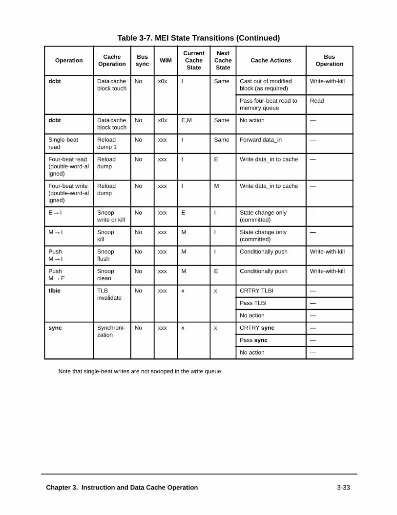
Note that single-beat writes are not snooped in the write queue.
dcbt Data cacheblock touch
No x0x I Same Cast out of modifiedblock (as required)
Write-with-kill
Pass four-beat read tomemory queue
Read
dcbt Data cacheblock touch
No x0x E,M Same No action —
Single-beatread
Reloaddump 1
No xxx I Same Forward data_in —
Four-beat read(double-word-aligned)
Reloaddump
No xxx I E Write data_in to cache —
Four-beat write(double-word-aligned)
Reloaddump
No xxx I M Write data_in to cache —
E→I Snoopwrite or kill
No xxx E I State change only(committed)
—
M→I Snoopkill
No xxx M I State change only(committed)
—
PushM→I
Snoopflush
No xxx M I Conditionally push Write-with-kill
PushM→E
Snoopclean
No xxx M E Conditionally push Write-with-kill
tlbie TLBinvalidate
No xxx x x CRTRY TLBI —
Pass TLBI —
No action —
sync Synchroni-zation
No xxx x x CRTRY sync —
Pass sync —
No action —
Table 3-7. MEI State Transitions (Continued)
OperationCache
OperationBussync
WIMCurrentCacheState
NextCacheState
Cache ActionsBus
Operation
Chapter 3. Instruction and Data Cache Operation 3-33

3-34 IBM PowerPC 740 / PowerPC 750 RISC Microprocessor User’s Manual

erPCation).e, thes the
te as arnalationbeginssing of
morethe
ister.
refore,, theytion-in theired tonterstially.occur,fully
toredption isken.ltiplery state
Chapter 4Exceptions4040
The OEA portion of the PowerPC architecture defines the mechanism by which Powprocessors implement exceptions (referred to as interrupts in the architecture specificException conditions may be defined at other levels of the architecture. For examplUISA defines conditions that may cause floating-point exceptions; the OEA definemechanism by which the exception is taken.
The PowerPC exception mechanism allows the processor to change to supervisor staresult of unusual conditions arising in the execution of instructions and from extesignals, bus errors, or various internal conditions. When exceptions occur, informabout the state of the processor is saved to certain registers and the processorexecution at an address (exception vector) predetermined for each exception. Procesexceptions begins in supervisor mode.
Although multiple exception conditions can map to a single exception vector, often aspecific condition may be determined by examining a register associated withexception—for example, the DSISR and the floating-point status and control reg(FPSCR). Also, software can explicitly enable or disable some exception conditions
The PowerPC architecture requires that exceptions be taken in program order; thealthough a particular implementation may recognize exception conditions out of orderare handled strictly in order with respect to the instruction stream. When an instruccaused exception is recognized, any unexecuted instructions that appear earlierinstruction stream, including any that have not yet entered the execute state, are requcomplete before the exception is taken. For example, if a single instruction encoumultiple exception conditions, those exceptions are taken and handled sequenLikewise, exceptions that are asynchronous and precise are recognized when theybut are not handled until all instructions currently in the execute stage successcomplete execution and report their results.
To prevent loss of state information, exception handlers must save the information sin the machine status save/restore registers, SRR0 and SRR1, soon after the excetaken to prevent this information from being lost due to another exception being taBecause exceptions can occur while an exception handler routine is executing, muexceptions can become nested. It is up to the exception handler to save the necessainformation if control is to return to the excepting program.
Chapter 4. Exceptions 4-1
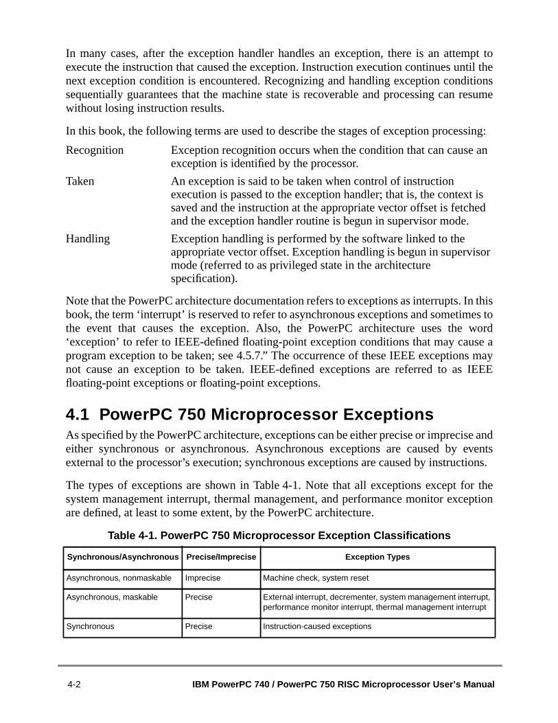
mpt totil theitionsresume
sing:
e an
t ised
sor
In thises toword
se as mayIEEE
ise andeventsctions.
r theeption
In many cases, after the exception handler handles an exception, there is an atteexecute the instruction that caused the exception. Instruction execution continues unnext exception condition is encountered. Recognizing and handling exception condsequentially guarantees that the machine state is recoverable and processing canwithout losing instruction results.
In this book, the following terms are used to describe the stages of exception proces
Recognition Exception recognition occurs when the condition that can causexception is identified by the processor.
Taken An exception is said to be taken when control of instructionexecution is passed to the exception handler; that is, the contexsaved and the instruction at the appropriate vector offset is fetchand the exception handler routine is begun in supervisor mode.
Handling Exception handling is performed by the software linked to theappropriate vector offset. Exception handling is begun in supervimode (referred to as privileged state in the architecturespecification).
Note that the PowerPC architecture documentation refers to exceptions as interrupts.book, the term ‘interrupt’ is reserved to refer to asynchronous exceptions and sometimthe event that causes the exception. Also, the PowerPC architecture uses the‘exception’ to refer to IEEE-defined floating-point exception conditions that may cauprogram exception to be taken; see 4.5.7.” The occurrence of these IEEE exceptionnot cause an exception to be taken. IEEE-defined exceptions are referred to asfloating-point exceptions or floating-point exceptions.
4.1 PowerPC 750 Microprocessor ExceptionsAs specified by the PowerPC architecture, exceptions can be either precise or impreceither synchronous or asynchronous. Asynchronous exceptions are caused byexternal to the processor’s execution; synchronous exceptions are caused by instru
The types of exceptions are shown in Table 4-1. Note that all exceptions except fosystem management interrupt, thermal management, and performance monitor excare defined, at least to some extent, by the PowerPC architecture.
Table 4-1. PowerPC 750 Microprocessor Exception Classifications
Synchronous/Asynchronous Precise/Imprecise Exception Types
Asynchronous, nonmaskable Imprecise Machine check, system reset
Asynchronous, maskable Precise External interrupt, decrementer, system management interrupt,performance monitor interrupt, thermal management interrupt
Synchronous Precise Instruction-caused exceptions
4-2 IBM PowerPC 740 / PowerPC 750 RISC Microprocessor User’s Manual

ing ofin the
These classifications are discussed in greater detail in 4.2.” For a better understandhow the 750 implements precise exceptions, see Chapter 6.” Exceptions implemented750, and conditions that cause them, are listed in Table 4-2.
Table 4-2. Exceptions and Conditions
Exception TypeVector Offset
(hex)Causing Conditions
Reserved 00000 —
System reset 00100 Assertion of either HRESET or SRESET or at power-on reset
Machine check 00200 Assertion of TEA during a data bus transaction, assertion of MCP, or anaddress, data, or L2 bus parity error. MSR[ME] must be set.
DSI 00300 As specified in the PowerPC architecture. For TLB misses on load, store, orcache operations, a DSI exception occurs if a page fault occurs.
ISI 00400 As defined by the PowerPC architecture
External interrupt 00500 MSR[EE] = 1 and INT is asserted
Alignment 00600 • A floating-point load/store, stmw , stwcx. , lmw , lwarx , eciwx , or ecowxinstruction operand is not word-aligned.
• A multiple/string load/store operation is attempted in little-endian mode• An operand of a dcbz instruction is on a page that is write-through or
cache-inhibited for a virtual mode access.• An attempt to execute a dcbz instruction occurs when the cache is
disabled.
Program 00700 As defined by the PowerPC architecture
Floating-pointunavailable
00800 As defined by the PowerPC architecture
Decrementer 00900 As defined by the PowerPC architecture, when the most-significant bit of theDEC register changes from 0 to 1 and MSR[EE] = 1
Reserved 00A00–00BFF —
System call 00C00 Execution of the System Call (sc ) instruction
Trace 00D00 MSR[SE] =1 or a branch instruction is completing and MSR[BE] =1. The 750differs from the OEA by not taking this exception on an isync .
Reserved 00E00 The 750 does not generate an exception to this vector. Other PowerPCprocessors may use this vector for floating-point assist exceptions.
Reserved 00E10–00EFF —
Performance monitor 00F00 The limit specified in PMCn is met and MMCR0[ENINT] = 1 (750-specific)
Instruction addressbreakpoint
01300 IABR[0–29] matches EA[0–29] of the next instruction to complete, IABR[TE]matches MSR[IR], and IABR[BE] = 1 (750-specific)
System managementinterrupt
01400 MSR[EE] = 1 and SMI is asserted (750-specific)
Reserved 01500–016FF —
Chapter 4. Exceptions 4-3

s—eption into
r
strict
e
ment,yed
up toate isuctioned. Ifnedoving
further
des
4.2 Exception Recognition and PrioritiesExceptions are roughly prioritized by exception class, as follows:
1. Nonmaskable, asynchronous exceptions have priority over all other exceptionsystem reset and machine check exceptions (although the machine check exccondition can be disabled so the condition causes the processor to go directlythe checkstop state). These exceptions cannot be delayed and do not wait focompletion of any precise exception handling.
2. Synchronous, precise exceptions are caused by instructions and are taken inprogram order.
3. Imprecise exceptions (imprecise mode floating-point enabled exceptions) arecaused by instructions and they are delayed until higher priority exceptions artaken. Note that the 750 does not implement an exception of this type.
4. Maskable asynchronous exceptions (external, decrementer, thermal managesystem management, performance monitor, and interrupt exceptions) are delauntil higher priority exceptions are taken.
The following list of exception categories describes how the 750 handles exceptionsthe point of signaling the appropriate interrupt to occur. Note that a recoverable streached if the completed store queue is empty (drained, not canceled) and any instrthat is next in program order and has been signaled to complete has completMSR[RI] = 0, the 750 is in a nonrecoverable state. Also, instruction completion is defias updating all architectural registers associated with that instruction, and then remthat instruction from the completion buffer.
• Exceptions caused by asynchronous events (interrupts). These exceptions aredistinguished by whether they are maskable and recoverable.— Asynchronous, nonmaskable, nonrecoverable
System reset for assertion ofHRESET—Has highest priority and is takenimmediately regardless of other pending exceptions or recoverability. (Inclupower-on reset)
Thermalmanagementinterrupt
01700 Thermal management is enabled, junction temperature exceeds the thresholdspecified in THRM1 or THRM2, and MSR[EE] = 1 (750-specific)
Reserved 01800–02FFF —
Table 4-2. Exceptions and Conditions (Continued)
Exception TypeVector Offset
(hex)Causing Conditions
4-4 IBM PowerPC 740 / PowerPC 750 RISC Microprocessor User’s Manual
f
en
l, and
her
ther
point
and
y bee alle ISI
tion orons
n. Iftakesenmes).
n ofcesst-
— Asynchronous, maskable, nonrecoverable
Machine check exception—Has priority over any other pending exceptionexcept system reset for assertion ofHRESET. Taken immediately regardless orecoverability.
— Asynchronous, nonmaskable, recoverable
System reset forSRESET—Has priority over any other pending exceptionexcept system reset forHRESET (or power-on reset), or machine check. Takimmediately when a recoverable state is reached.
— Asynchronous, maskable, recoverable
System management, performance monitor, thermal management, externadecrementer interrupts—Before handling this type of exception, the nextinstruction in program order must complete. If that instruction causes anottype of exception, that exception is taken and the asynchronous, maskablerecoverable exception remains pending, until the instruction completes. Furinstruction completion is halted. The asynchronous, maskable recoverableexception is taken when a recoverable state is reached.
• Instruction-related exceptions. These exceptions are further organized into thein instruction processing in which they generate an exception.— Instruction fetch
ISI exceptions—Once this type of exception is detected, dispatching stopsthe current instruction stream is allowed to drain out of the machine. Ifcompleting any of the instructions in this stream causes an exception, thatexception is taken and the instruction fetch exception is discarded (but maencountered again when instruction processing resumes). Otherwise, oncpending instructions have executed and a recoverable state is reached, thexception is taken.
— Instruction dispatch/execution
Program, DSI, alignment, floating-point unavailable, system call, and instrucaddress breakpoint—This type of exception is determined during dispatchexecution of an instruction. The exception remains pending until all instructibefore the exception-causing instruction in program order complete. Theexception is then taken without completing the exception-causing instructiocompleting these previous instructions causes an exception, that exceptionpriority over the pending instruction dispatch/execution exception, which is thdiscarded (but may be encountered again when instruction processing resu
— Post-instruction execution
Trace—Trace exceptions are generated following execution and completioan instruction while trace mode is enabled. If executing the instruction produconditions for another type of exception, that exception is taken and the poinstruction exception is forgotten for that instruction.
Chapter 4. Exceptions 4-5

ed, as
Note that these exception classifications correspond to how exceptions are prioritizdescribed in Table 4-3.Table 4-3. PowerPC 750 Exception Priorities
Priority Exception Cause
Asynchronous Exceptions (Interrupts)
0 System reset Power on reset, assertion of HRESET and TRST (hard reset)
1 Machine check Any enabled machine check condition (L1 address or data parity error, L2 dataparity error, assertion of TEA or MCP)
2 System reset Assertion of SRESET (soft reset)
3 System management Assertion of SMI
4 External interrupt Assertion of INT
5 Performance monitor Any programmer-specified performance monitor condition
6 Decrementer Decrementer passes through zero
7 Thermal management Any programmer-specified thermal management condition
Instruction Fetch Exceptions
0 ISI Any ISI exception condition
Instruction Dispatch/Execution Exceptions
0 Instruction addressbreakpoint
Any instruction address breakpoint exception condition
1 Program Occurrence of an illegal instruction, privileged instruction, or trap exceptioncondition. Note that floating-point enabled program exceptions have lower priority.
2 System call System Call (sc ) instruction
3 Floating-pointunavailable
Any floating-point unavailable exception condition
4 Program A floating-point enabled exception condition (lowest-priority program exception)
5 DSI DSI exception due to eciwx , ecowx with EAR[E] = 0 (DSISR[11]). Lower priorityDSI exception conditions are shown below.
6 Alignment Any alignment exception condition, prioritized as follows:1 Floating-point access not word-aligned2 lmw , stmw , lwarx , stwcx. not word-aligned3 eciwx or ecowx not word-aligned4 Multiple or string access with MSR[LE] set5 dcbz to write-through or cache-inhibited page or cache is disabled
7 DSI BAT page protection violation
8 DSI Any access except cache operations to a segment where SR[T] = 1 (DSISR[5]) oran access crosses from a T = 0 segment to one where T = 1 (DSISR[5])
9 DSI TLB page protection violation
10 DSI DABR address match
4-6 IBM PowerPC 740 / PowerPC 750 RISC Microprocessor User’s Manual

ed evenption
may
ts of theafter
ructionuptedddressveay bese of a
bits as
ecificR1.
System reset and machine check exceptions may occur at any time and are not delayif an exception is being handled. As a result, state information for an interrupted excemay be lost; therefore, these exceptions are typically nonrecoverable. An exceptionnot be taken immediately when it is recognized.
4.3 Exception ProcessingWhen an exception is taken, the processor uses SRR0 and SRR1 to save the contenMSR for the current context and to identify where instruction execution should resumethe exception is handled.
When an exception occurs, the address saved in SRR0 helps determine where instprocessing should resume when the exception handler returns control to the interrprocess. Depending on the exception, this may be the address in SRR0 or at the next ain the program flow. All instructions in the program flow preceding this one will hacompleted execution and no subsequent instruction will have begun execution. This mthe address of the instruction that caused the exception or the next one (as in the casystem call, trace, or trap exception). The SRR0 register is shown in Figure 4-1.
Figure 4-1. Machine Status Save/Restore Register 0 (SRR0)
SRR1 is used to save machine status (selected MSR bits and possibly other statuswell) on exceptions and to restore those values when anrfi instruction is executed. SRR1is shown in Figure 4-2.
Figure 4-2. Machine Status Save/Restore Register 1 (SRR1)
For most exceptions, bits 2–4 and 10–12 of SRR1 are loaded with exception-spinformation and MSR[5–9, 16–31] are placed into the corresponding bit positions of SR
Post-Instruction Execution Exceptions
11 Trace MSR[SE] = 1 (or MSR[BE] = 1 for branches)
Table 4-3. PowerPC 750 Exception Priorities (Continued)
Priority Exception Cause
SRR0 (Holds EA for Instruction in Interrupted Program Flow)
0 31
Exception-Specific Information and MSR Bit Values
0 31
Chapter 4. Exceptions 4-7
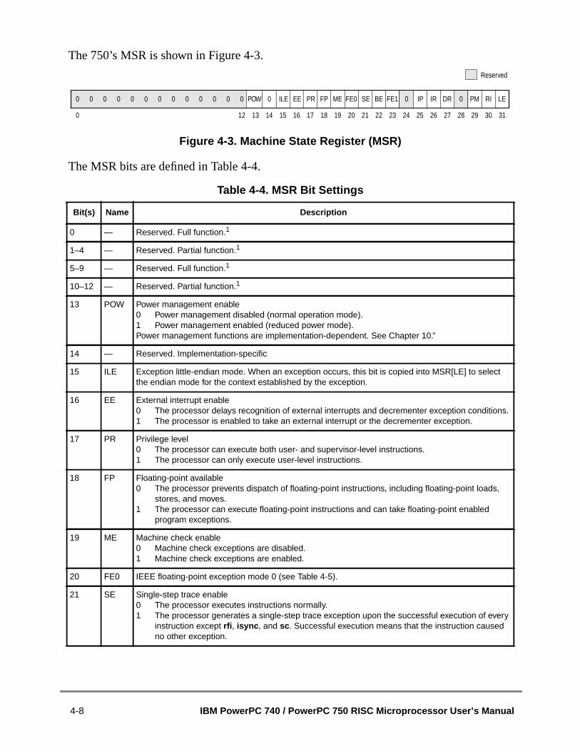
The 750’s MSR is shown in Figure 4-3.
Figure 4-3. Machine State Register (MSR)
The MSR bits are defined in Table 4-4.
Table 4-4. MSR Bit Settings
Bit(s) Name Description
0 — Reserved. Full function.1
1–4 — Reserved. Partial function.1
5–9 — Reserved. Full function.1
10–12 — Reserved. Partial function.1
13 POW Power management enable0 Power management disabled (normal operation mode).1 Power management enabled (reduced power mode).Power management functions are implementation-dependent. See Chapter 10.”
14 — Reserved. Implementation-specific
15 ILE Exception little-endian mode. When an exception occurs, this bit is copied into MSR[LE] to selectthe endian mode for the context established by the exception.
16 EE External interrupt enable0 The processor delays recognition of external interrupts and decrementer exception conditions.1 The processor is enabled to take an external interrupt or the decrementer exception.
17 PR Privilege level0 The processor can execute both user- and supervisor-level instructions.1 The processor can only execute user-level instructions.
18 FP Floating-point available0 The processor prevents dispatch of floating-point instructions, including floating-point loads,
stores, and moves.1 The processor can execute floating-point instructions and can take floating-point enabled
program exceptions.
19 ME Machine check enable0 Machine check exceptions are disabled.1 Machine check exceptions are enabled.
20 FE0 IEEE floating-point exception mode 0 (see Table 4-5).
21 SE Single-step trace enable0 The processor executes instructions normally.1 The processor generates a single-step trace exception upon the successful execution of every
instruction except rfi , isync , and sc . Successful execution means that the instruction causedno other exception.
ILE EE PR SEFE0 BE IP IR
0 12 13 14 15 16 17 18 19 20 21 22 23 24 25 26 27 28 29 30 31
PM0
Reserved
LERIDR0FE1MEFP0POW0 000000000000
4-8 IBM PowerPC 740 / PowerPC 750 RISC Microprocessor User’s Manual
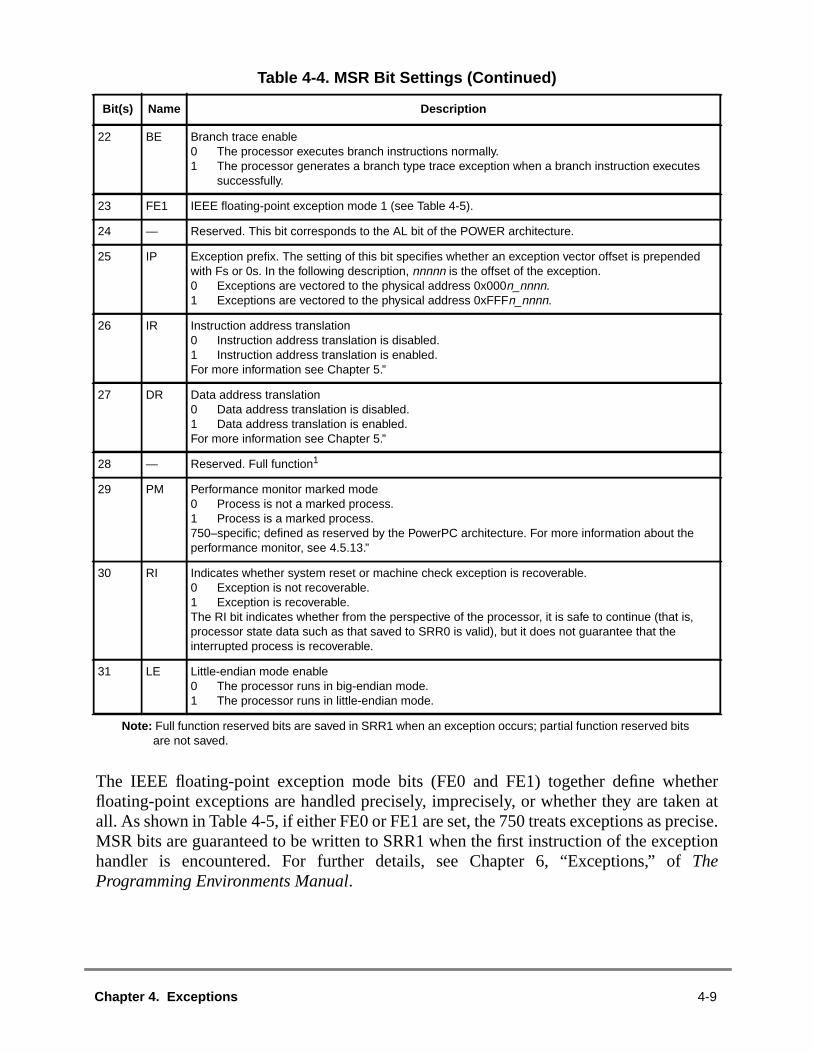
theren atecise.ption
The IEEE floating-point exception mode bits (FE0 and FE1) together define whefloating-point exceptions are handled precisely, imprecisely, or whether they are takall. As shown in Table 4-5, if either FE0 or FE1 are set, the 750 treats exceptions as prMSR bits are guaranteed to be written to SRR1 when the first instruction of the excehandler is encountered. For further details, see Chapter 6, “Exceptions,” ofTheProgramming Environments Manual.
22 BE Branch trace enable0 The processor executes branch instructions normally.1 The processor generates a branch type trace exception when a branch instruction executes
successfully.
23 FE1 IEEE floating-point exception mode 1 (see Table 4-5).
24 — Reserved. This bit corresponds to the AL bit of the POWER architecture.
25 IP Exception prefix. The setting of this bit specifies whether an exception vector offset is prependedwith Fs or 0s. In the following description, nnnnn is the offset of the exception.0 Exceptions are vectored to the physical address 0x000n_nnnn.1 Exceptions are vectored to the physical address 0xFFFn_nnnn.
26 IR Instruction address translation0 Instruction address translation is disabled.1 Instruction address translation is enabled.For more information see Chapter 5.”
27 DR Data address translation0 Data address translation is disabled.1 Data address translation is enabled.For more information see Chapter 5.”
28 — Reserved. Full function1
29 PM Performance monitor marked mode0 Process is not a marked process.1 Process is a marked process.750–specific; defined as reserved by the PowerPC architecture. For more information about theperformance monitor, see 4.5.13.”
30 RI Indicates whether system reset or machine check exception is recoverable.0 Exception is not recoverable.1 Exception is recoverable.The RI bit indicates whether from the perspective of the processor, it is safe to continue (that is,processor state data such as that saved to SRR0 is valid), but it does not guarantee that theinterrupted process is recoverable.
31 LE Little-endian mode enable0 The processor runs in big-endian mode.1 The processor runs in little-endian mode.
Note: Full function reserved bits are saved in SRR1 when an exception occurs; partial function reserved bitsare not saved.
Table 4-4. MSR Bit Settings (Continued)
Bit(s) Name Description
Chapter 4. Exceptions 4-9

rmined
red
ofn an.
topheckich is
tion-nd bydoes
tion.sed
first
4.3.1 Enabling and Disabling ExceptionsWhen a condition exists that may cause an exception to be generated, it must be detewhether the exception is enabled for that condition.
• IEEE floating-point enabled exceptions (a type of program exception) are ignowhen both MSR[FE0] and MSR[FE1] are cleared. If either bit is set, all IEEEenabled floating-point exceptions are taken and cause a program exception.
• Asynchronous, maskable exceptions (such as the external and decrementerinterrupts) are enabled by setting MSR[EE]. When MSR[EE] = 0, recognition these exception conditions is delayed. MSR[EE] is cleared automatically wheexception is taken to delay recognition of conditions causing those exceptions
• A machine check exception can occur only if the machine check enable bit,MSR[ME], is set. If MSR[ME] is cleared, the processor goes directly into checksstate when a machine check exception condition occurs. Individual machine cexceptions can be enabled and disabled through bits in the HID0 register, whdescribed in Table 4-10.
• System reset exceptions cannot be masked.
4.3.2 Steps for Exception ProcessingAfter it is determined that the exception can be taken (by confirming that any instruccaused exceptions occurring earlier in the instruction stream have been handled, aconfirming that the exception is enabled for the exception condition), the processorthe following:
1. SRR0 is loaded with an instruction address that depends on the type of excepSee the individual exception description for details about how this register is ufor specific exceptions.
2. SRR1[1–4, 10–15] are loaded with information specific to the exception type.
3. SRR1[5–9, 16–31] are loaded with a copy of the corresponding MSR bits.Depending on the implementation, reserved bits may not be copied.
4. The MSR is set as described in Table 4-4. The new values take effect as the instruction of the exception-handler routine is fetched.
Table 4-5. IEEE Floating-Point Exception Mode Bits
FE0 FE1 Mode
0 0 Floating-point exceptions disabled
0 1 Imprecise nonrecoverable. For this setting, the 750 operates in floating-point precise mode.
1 0 Imprecise recoverable. For this setting, the 750 operates in floating-point precise mode.
1 1 Floating-point precise mode
4-10 IBM PowerPC 740 / PowerPC 750 RISC Microprocessor User’s Manual

,
ionion'sred,
ect to
hat aset
and
ughot
gss. In
usetion,
and
this
s,” of
Note that MSR[IR] and MSR[DR] are cleared for all exception types; thereforeaddress translation is disabled for both instruction fetches and data accessesbeginning with the first instruction of the exception-handler routine.
5. Instruction fetch and execution resumes, using the new MSR value, at a locatspecific to the exception type. The location is determined by adding the exceptvector (see Table 4-2) to the base address determined by MSR[IP]. If IP is cleaexceptions are vectored to the physical address 0x000n_nnnn. If IP is set, exceptionsare vectored to the physical address 0xFFFn_nnnn. For a machine check exceptionthat occurs when MSR[ME] = 0 (machine check exceptions are disabled), thecheckstop state is entered (the machine stops executing instructions). See .”
4.3.3 Setting MSR[RI]An operating system may handle MSR[RI] as follows:
• In the machine check and system reset exceptions—If MSR[RI] is cleared, thexception is not recoverable. If it is set, the exception is recoverable with respethe processor.
• In each exception handler—When enough state information has been saved tmachine check or system reset exception can reconstruct the previous state, MSR[RI].
• In each exception handler—Clear MSR[RI], set SRR0 and SRR1 appropriately,then executerfi .
• Note that the RI bit being set indicates that, with respect to the processor, enoprocessor state data remains valid for the processor to continue, but it does nguarantee that the interrupted process can resume.
4.3.4 Returning from an Exception HandlerThe Return from Interrupt (rfi ) instruction performs context synchronization by allowinpreviously-issued instructions to complete before returning to the interrupted procegeneral, execution of therfi instruction ensures the following:
• All previous instructions have completed to a point where they can no longer caan exception. If a previous instruction causes a direct-store interface error excepthe results must be determined before this instruction is executed.
• Previous instructions complete execution in the context (privilege, protection, address translation) under which they were issued.
• Therfi instruction copies SRR1 bits back into the MSR.
• Instructions fetched after this instruction execute in the context established byinstruction.
• Program execution resumes at the instruction indicated by SRR0
For a complete description of context synchronization, refer to Chapter 6, “ExceptionThe Programming Environments Manual.
Chapter 4. Exceptions 4-11

ing:
r
d (ornd
ttingson the
4.4 Process SwitchingThe following instructions are useful for restoring proper context during process switch
• Thesync instruction orders the effects of instruction execution. All instructionspreviously initiated appear to have completed before thesyncinstruction completes,and no subsequent instructions appear to be initiated until thesync instructioncompletes. For an example showing use ofsync, see Chapter 2, “PowerPC RegisteSet,” ofThe Programming Environments Manual.
• The isync instruction waits for all previous instructions to complete and thendiscards any fetched instructions, causing subsequent instructions to be fetcherefetched) from memory and to execute in the context (privilege, translation, aprotection) established by the previous instructions.
• Thestwcx. instruction clears any outstanding reservations, ensuring that anlwarxinstruction in an old process is not paired with anstwcx. instruction in a new one.
The operating system should set MSR[RI] as described in 4.3.3.”
4.5 Exception DefinitionsTable 4-6 shows all the types of exceptions that can occur with the 750 and MSR sewhen the processor goes into supervisor mode due to an exception. Dependingexception, certain of these bits are stored in SRR1 when an exception is taken.
Table 4-6. MSR Setting Due to Exception
Exception TypeMSR Bit 1
POW ILE EE PR FP ME FE0 SE BE FE1 IP IR DR PM RI LE
System reset 0 — 0 0 0 — 0 0 0 0 — 0 0 0 0 ILE
Machine check 0 — 0 0 0 0 0 0 0 0 — 0 0 0 0 ILE
DSI 0 — 0 0 0 — 0 0 0 0 — 0 0 0 0 ILE
ISI 0 — 0 0 0 — 0 0 0 0 — 0 0 0 0 ILE
External interrupt 0 — 0 0 0 — 0 0 0 0 — 0 0 0 0 ILE
Alignment 0 — 0 0 0 — 0 0 0 0 — 0 0 0 0 ILE
Program 0 — 0 0 0 — 0 0 0 0 — 0 0 0 0 ILE
Floating-point unavailable 0 — 0 0 0 — 0 0 0 0 — 0 0 0 0 ILE
Decrementer interrupt 0 — 0 0 0 — 0 0 0 0 — 0 0 0 0 ILE
System call 0 — 0 0 0 — 0 0 0 0 — 0 0 0 0 ILE
Trace exception 0 — 0 0 0 — 0 0 0 0 — 0 0 0 0 ILE
System management 0 — 0 0 0 — 0 0 0 0 — 0 0 0 0 ILE
Performance monitor 0 — 0 0 0 — 0 0 0 0 — 0 0 0 0 ILE
Thermal management 0 — 0 0 0 — 0 0 0 0 — 0 0 0 0 ILE
4-12 IBM PowerPC 740 / PowerPC 750 RISC Microprocessor User’s Manual

If the
ndler
ecturealed totion is
softset thismining
ll
The setting of the exception prefix bit (IP) determines how exceptions are vectored.bit is cleared, exceptions are vectored to the physical address 0x000n_nnnn(wherennnnnis the vector offset); if IP is set, exceptions are vectored to physical address 0xFFFn_nnnn.Table 4-2 shows the exception vector offset of the first instruction of the exception haroutine for each exception type.
4.5.1 System Reset Exception (0x00100)The 750 implements the system reset exception as defined in the PowerPC archit(OEA). The system reset exception is a nonmaskable, asynchronous exception signthe processor through the assertion of system-defined signals. In the 750, the excepsignaled by the assertion of either the soft reset (SRESET) or hard reset (HRESET) inputs,described more fully in Chapter 7.”
The 750 implements HID0[NHR], which helps software distinguish a hard reset from areset. Because this bit is cleared by a hard reset, but not by a soft reset, software canbit after a hard reset and tell whether a subsequent reset is a hard or soft reset by exawhether this bit is still set. See 2.1.2.2.”
The first bus operation following the negation ofHRESET or the assertion of SRESET wibe a single-beat instruction fetch (caching will be inhibited) to x00100.
Table 4-7 lists register settings when a system reset exception is taken.
Note:1. 0 Bit is cleared.
ILEBit is copied from the MSR[ILE].— Bit is not alteredReserved bits are read as if written as 0.
Table 4-7. System Reset Exception—Register Settings
Register Setting Description
SRR0 Set to the effective address of the instruction that the processor would have attempted to execute nextif no exception conditions were present.
SRR1 0 Loaded with equivalent MSR bits1–4 Cleared5–9 Loaded with equivalent MSR bits10–15 Cleared16–31 Loaded with equivalent MSR bitsNote that if the processor state is corrupted to the extent that execution cannot resume reliably,MSR[RI] (SRR1[30]) is cleared.
Table 4-6. MSR Setting Due to Exception (Continued)
Exception TypeMSR Bit 1
POW ILE EE PR FP ME FE0 SE BE FE1 IP IR DR PM RI LE
Chapter 4. Exceptions 4-13

e 750tion,rain.
erPCffset,eitherand
e does
sertedare
tion.
s ofAGon on
sesation
4.5.1.1 Soft ResetIf SRESET is asserted, the processor is first put in a recoverable state. To do this, thallows any instruction at the point of completion to either complete or take an excepblocks completion of any following instructions, and allows the completion queue to dThe state before the exception occurred is then saved as specified in the Powarchitecture and instruction fetching begins at the system reset interrupt vector o0x00100. The vector address on a soft reset depends on the setting of MSR[IP] (0x0000_0100 or 0xFFF0_0100). Soft resets are third in priority, after hard resetmachine check. This exception is recoverable provided attaining a recoverable statnot generate a machine check.
SRESET is an effectively edge-sensitive signal that can be asserted and deasasynchronously, provided the minimum pulse width specified in the hardwspecifications is met. AssertingSRESET causes the 750 to take a system reset excepThis exception modifies the MSR, SRR0, and SRR1, as described inThe ProgrammingEnvironments Manual. Unlike hard reset, soft reset does not directly affect the stateoutput signals. Attempts to useSRESET during a hard reset sequence or while the JTlogic is non-idle cause unpredictable results (see Section 7.2.9.6.2 for more informatisoft reset).
SRESET can be asserted duringHRESET assertion (see Figure 4-4). In all three cashown in Figure 4-4, theSRESET assertion and deassertion have no effect on the operor state of the machine.SRESET asserted coincident to, or after the assertion of,HRESETwill also have no effect on the operation or state of the machine.
Figure 4-4. SRESET Asserted During HRESET
MSR POW 0ILE —EE 0PR 0
FP 0ME —FE0 0SE 0
BE 0FE1 0IP —IR 0
DR 0PM 0RI 0LE Set to value of ILE
Table 4-7. System Reset Exception—Register Settings (Continued)
HRESETSRESET
HRESETSRESET
HRESETSRESET
OK
OK
OK
4-14 IBM PowerPC 740 / PowerPC 750 RISC Microprocessor User’s Manual

ntart a
ainreset.lected
er IOset
thens
n hard
. Whenes toighestf thehardered.mayrrect
4.5.1.2 Hard ResetA hard reset is initiated by assertingHRESET. Hard reset is used primarily for power-oreset (POR) (in which caseTRST must also be asserted), but it can also be used to resrunning processor. TheHRESET signal must be asserted during power up and must remasserted for a period that allows the PLL to achieve lock and the internal logic to beThis period is specified in the hardware specifications. Table 4-8 shows the state of se750 signals during HRESET (whileHRESET is held asserted) and fromHRESETdeassertion until the L2 interface is enabled. Unless noted, the 750 tri-states all othdrivers within five clocks ofHRESET assertion The 750 internal state after the hard reinterval is defined in Table 4-9. IfHRESET is asserted for less than this amount of time,results are not predictable. IfHRESET is asserted during normal operation, all operatiocease, and the machine state is lost (see Section 7.2.9.6.1 for more information oreset).
The hard reset exception is a nonrecoverable, nonmaskable asynchronous exceptionHRESET is asserted or at power-on reset (POR), the 750 immediately branch0xFFF0_0100 without attempting to reach a recoverable state. A hard reset has the hpriority of any exception. It is always nonrecoverable. Table 4-9 shows the state omachine just before it fetches the first instruction of the system reset handler after areset. In Table 4-9, the term “Unknown” means that the content may have been disordThese facilities must be properly initialized before use. The FPRs, BATs, and TLBshave been disordered. To initialize the BATs, first set them all to zero, then to the covalues before any address translation occurs.
Table 4-8. HRESET Signal States
Signal NameDuringHRESET
HRESET Deassertion to L2Enabled
L2ADDR hi-z 0
L2DATA hi-z 0
L2DP hi-z 0
L2CE 1 1
L2WE 1 1
L2LCK_OUTA 0 0
L2LCK_OUTB 0 0
L2SYNC_OUT 0 0
L2ZZ 0 0
Chapter 4. Exceptions 4-15

Table 4-9. Settings Caused by Hard Reset
Register Setting Register Setting
GPRs Unknown PVR see the PowerPC 740 andPowerPC 750 EmbeddedMicroprocessor: HardwareSpecifications
FPRs Unknown HID0 00000000
FPSCR 00000000 HID1 00000000
CR All 0s DMISS andIMISS
All 0s
SRs Unknown DCMP andICMP
All 0s
MSR 00000040 (only IP set) RPA All 0s
XER 00000000 IABR All 0s (break point disabled)
TBU 00000000 DSISR 00000000
TBL 00000000 DAR 00000000
LR 00000000 DEC FFFFFFFF
CTR 00000000 HASH1 00000000
SDR1 00000000 HASH2 00000000
SRR0 00000000 TLBs Unknown
SRR1 00000000 ReservationAddress
Unknown (reservation flag-cleared)
SPRGs 00000000 BATs Unknown
Tag directory,Icache, andDcache
All entries are marked invalid,all LRU bits are set to 0, andcaches are disabled.
Cache, Icache,and Dcache
All blocks are unchanged frombefore HRESET.
DABR Breakpoint is disabled.Address is unknown.
L2_CR 00000000
MMCRn 00000000
THRMn 00000000
UMMCRn 00000000
UPMCn 00000000
USIA 00000000
XER 00000000
PMCn Unknown
ICTC 00000000
4-16 IBM PowerPC 740 / PowerPC 750 RISC Microprocessor User’s Manual

or
DR]de
ecturearitynsferupten if
ts, as
The following is also true after a hard reset operation:
• External checkstops are enabled.• The on-chip test interface has given control of the I/Os to the rest of the chip f
functional use.• Since the reset exception has data and instruction translation disabled (MSR[
and MSR[IR] both cleared), the chip operates in direct address translation mo(referred to as the real addressing mode in the architecture specification).
• Time from HRESET deassertion until the 750 asserts the firstTS (bus parked on the750) orBG is 8 to 12 bus clocks (SYSCLK).
4.5.2 Machine Check Exception (0x00200)The 750 implements the machine check exception as defined in the PowerPC archit(OEA). It conditionally initiates a machine check exception after an address or data perror occurred on the bus or in either the L1 or L2 cache, after receiving a qualified traerror acknowledge (TEA) indication on the 750 bus, or after the machine check interr(MCP) signal had been asserted. As defined in the OEA, the exception is not takMSR[ME] is cleared, in which case the processor enters checkstop state.
Certain machine check conditions can be enabled and disabled using HID0 bidescribed in Table 4-10.
Table 4-10. HID0 Machine Check Enable Bits
Bit Name Function
0 EMCP Enable MCP. The primary purpose of this bit is to mask out further machine check exceptions causedby assertion of MCP, similar to how MSR[EE] can mask external interrupts.0 Masks MCP. Asserting MCP does not generate a machine check exception or a checkstop.1 Asserting MCP causes a checkstop if MSR[ME] = 0 or a machine check exception if MSR[ME] = 1.
1 DBP Enable/disable 60x bus address and data parity generation.0 If address or data parity is not used by the system and the respective parity checking is disabled
(HID0[EBA] or HID0[EBD] = 0), input receivers for those signals are disabled, do not require pull-upresistors, and therefore should be left unconnected. If all parity generation is disabled, all paritychecking should also be disabled and parity signals need not be connected.
1 Parity generation is enabled.
2 EBA Enable/disable 60x bus address parity checking.0 Prevents address parity checking.1 Allows a address parity error to cause a checkstop if MSR[ME] = 0 or a machine check exception if
MSR[ME] = 1.EBA and EBD allow the processor to operate with memory subsystems that do not generate parity.
3 EBD Enable 60x bus data parity checking0 Parity checking is disabled.1 Allows a data parity error to cause a checkstop if MSR[ME] = 0 or a machine check exception if
MSR[ME] = 1.EBA and EBD allow the processor to operate with memory subsystems that do not generate parity.
15 NHR Not hard reset (software use only)0 A hard reset occurred if software had previously set this bit1 A hard reset has not occurred.
Chapter 4. Exceptions 4-17

theat at the
the
anden theerates
ress,
achinemory.urces
thesor
heck
cannotd the
A TEA indication on the bus can result from any load or store operation initiated byprocessor. In general,TEA is expected to be used by a memory controller to indicate thmemory parity error or an uncorrectable memory ECC error has occurred. Note tharesulting machine check exception is imprecise and unordered with respect toinstruction that originated the bus operation.
If MSR[ME] and the appropriate HID0 bits are set, the exception is recognizedhandled; otherwise, the processor generates an internal checkstop condition. Whexception is recognized, all incomplete stores are discarded. The bus protocol opnormally.
A machine check exception may result from referencing a nonexistent physical addeither directly (with MSR[DR] = 0) or through an invalid translation. If adcbz instructionintroduces a block into the cache associated with a nonexistent physical address, a mcheck exception can be delayed until an attempt is made to store that block to main meNot all PowerPC processors provide the same level of error checking. Checkstop soare implementation-dependent.
Machine check exceptions are enabled when MSR[ME] = 1; this is described infollowing section, 4.5.2.1.” If MSR[ME] = 0 and a machine check occurs, the procesenters the checkstop state. Checkstop state is described in 4.5.2.2.”
4.5.2.1 Machine Check Exception Enabled (MSR[ME] = 1)Machine check exceptions are enabled when MSR[ME] = 1. When a machine cexception is taken, registers are updated as shown in Table 4-11.
The machine check exception is usually unrecoverable in the sense that executionresume in the context that existed before the exception. If the condition that cause
Table 4-11. Machine Check Exception—Register Settings
Register Setting Description
SRR0 On a best-effort basis the 750 can set this to an EA of some instruction that was executing or about to beexecuting when the machine check condition occurred.
SRR1 0–10 Cleared11 Set when an L2 data cache parity error is detected, otherwise zero12 Set when MCP signal is asserted, otherwise zero13 Set when TEA signal is asserted, otherwise zero14 Set when a data bus parity error is detected, otherwise zero15 Set when an address bus parity error is detected, otherwise zero16–31 MSR[16–31]
MSR POW 0ILE —EE 0PR 0
FP 0ME 0FE0 0SE 0
BE 0FE1 0IP —IR 0
DR 0PM 0RI 0LE Set to value of ILE
Note that to handle another machine check exception, the exception handler should set MSR[ME] as soonas it is practical after a machine check exception is taken. Otherwise, subsequent machine check excep-tions cause the processor to enter the checkstop state.
4-18 IBM PowerPC 740 / PowerPC 750 RISC Microprocessor User’s Manual

allowdress.se thecheck
0200
ate. Inby
nerallyfrozen
itionefinedache
page
-storementwerPC
tionalkpointilitycture
fetcherPC
machine check does not otherwise prevent continued execution, MSR[ME] is set tothe processor to continue execution at the machine check exception vector adTypically, earlier processes cannot resume; however, operating systems can umachine check exception handler to try to identify and log the cause of the machinecondition.
When a machine check exception is taken, instruction fetching resumes at offset 0x0from the physical base address indicated by MSR[IP].
4.5.2.2 Checkstop State (MSR[ME] = 0)If MSR[ME] = 0 and a machine check occurs, the processor enters the checkstop staddition, the assertion ofCKSTP_IN to the 750 causes checkstop. Also, if enabledL2CR (L2DRO), a DLL rollover causes checkstop.
When a processor is in checkstop state, instruction processing is suspended and gecannot resume without the processor being reset. The contents of all latches arewithin two cycles upon entering checkstop state.
4.5.3 DSI Exception (0x00300)A DSI exception occurs when no higher priority exception exists and an error condrelated to a data memory access occurs. The DSI exception is implemented as it is din the PowerPC architecture (OEA). In case of a TLB miss for a load, store, or coperation, a DSI exception is taken if the resulting hardware table search causes afault.
On the 750, a DSI exception is taken when a load or store is attempted to a directsegment (SR[T] = 1). In the 750, a floating-point load or store to a direct-store segcauses a DSI exception rather than an alignment exception, as specified by the Poarchitecture.
The 750 also implements the data address breakpoint facility, which is defined as opin the PowerPC architecture and is supported by the optional data address brearegister (DABR). Although the architecture does not strictly prescribe how this facmust be implemented, the 750 follows the recommendations provided by the architeand described in the Chapter 2, “Programming Model,” and Chapter 6 “Exceptions,” inTheProgramming Environments Manual.
4.5.4 ISI Exception (0x00400)An ISI exception occurs when no higher priority exception exists and an attempt tothe next instruction fails. This exception is implemented as it is defined by the Powarchitecture (OEA), and is taken for the following conditions:
• The effective address cannot be translated.• The fetch access is to a no-execute segment (SR[N] = 1).• The fetch access is to guarded storage and MSR[IR] = 1.
Chapter 4. Exceptions 4-19

the
rruptrnalotm can
needtionsefined
] isbed in
ffset
cture
a DSIre. For
cturee or
• The fetch access is to a segment for which SR[T] is set.• The fetch access violates memory protection.
When an ISI exception is taken, instruction fetching resumes at offset 0x00400 fromphysical base address indicated by MSR[IP].
4.5.5 External Interrupt Exception (0x00500)An external interrupt is signaled to the processor by the assertion of the external intesignal (INT). TheINT signal is expected to remain asserted until the 750 takes the exteinterrupt exception. IfINT is negated early, recognition of the interrupt request is nguaranteed. After the 750 begins execution of the external interrupt handler, the systesafely negate theINT. When the 750 detects assertion ofINT, it stops dispatching and waitsfor all pending instructions to complete. This allows any instructions in progress thatto take an exception to do so before the external interrupt is taken. After all instruchave vacated the completion buffer, the 750 takes the external interrupt exception as din the PowerPC architecture (OEA).
An external interrupt may be delayed by other higher priority exceptions or if MSR[EEcleared when the exception occurs. Register settings for this exception are descriChapter 6, “Exceptions,” inThe Programming Environments Manual.
When an external interrupt exception is taken, instruction fetching resumes at o0x00500 from the physical base address indicated by MSR[IP].
4.5.6 Alignment Exception (0x00600)The 750 implements the alignment exception as defined by the PowerPC archite(OEA). An alignment exception is initiated when any of the following occurs:
• The operand of a floating-point load or store is not word-aligned.• The operand oflmw, stmw, lwarx , orstwcx. is not word-aligned.• The operand ofdcbz is in a page that is write-through or cache-inhibited.• An attempt is made to executedcbz when the data cache is disabled.• An eciwx or ecowx is not word-aligned• A multiple or string access is attempted with MSR[LE] set
Note that in the 750, a floating-point load or store to a direct-store segment causesexception rather than an alignment exception, as specified by the PowerPC architectumore information, see 4.5.3.”
4.5.7 Program Exception (0x00700)The 750 implements the program exception as it is defined by the PowerPC archite(OEA). A program exception occurs when no higher priority exception exists and onmore of the exception conditions defined in the OEA occur.
4-20 IBM PowerPC 740 / PowerPC 750 RISC Microprocessor User’s Manual

anythe
mition
tes that
ide ahese
by the), all
from
erPCritydingthed in
offset
erPCists, ar haster isn are
0900
,cture.
The 750 invokes the system illegal instruction program exception when it detectsinstruction from the illegal instruction class. The 750 fully decodes the SPR field ofinstruction. If an undefined SPR is specified, a program exception is taken.
The UISA definesmtspr and mfspr with the record bit (Rc) set as causing a prograexception or giving a boundedly-undefined result. In the 750, the appropriate condregister (CR) should be treated as undefined. Likewise, the PowerPC architecture stathe Floating Compared Unordered (fcmpu) or Floating Compared Ordered (fcmpo)instruction with the record bit set can either cause a program exception or provboundedly-undefined result. In the 750, an the BF field in an instruction encoding for tcases is considered undefined.
The 750 does not support either of the two floating-point imprecise modes supportedPowerPC architecture. Unless exceptions are disabled (MSR[FE0] = MSR[FE1] = 0floating-point exceptions are treated as precise.
When a program exception is taken, instruction fetching resumes at offset 0x00700the physical base address indicated by MSR[IP]. Chapter 6, “Exceptions,” inTheProgramming Environments Manualdescribes register settings for this exception.
4.5.8 Floating-Point Unavailable Exception (0x00800)The floating-point unavailable exception is implemented as defined in the Powarchitecture. A floating-point unavailable exception occurs when no higher prioexception exists, an attempt is made to execute a floating-point instruction (inclufloating-point load, store, or move instructions), and the floating-point available bit inMSR is disabled, (MSR[FP] = 0). Register settings for this exception are describeChapter 6, “Exceptions,” inThe Programming Environments Manual.
When a floating-point unavailable exception is taken, instruction fetching resumes at0x00800 from the physical base address indicated by MSR[IP].
4.5.9 Decrementer Exception (0x00900)The decrementer exception is implemented in the 750 as it is defined by the Powarchitecture. The decrementer exception occurs when no higher priority exception exdecrementer exception condition occurs (for example, the decrementer registecompleted decrementing), and MSR[EE] = 1. In the 750, the decrementer regisdecremented at one fourth the bus clock rate. Register settings for this exceptiodescribed in Chapter 6, “Exceptions,” inThe Programming Environments Manual.
When a decrementer exception is taken, instruction fetching resumes at offset 0x0from the physical base address indicated by MSR[IP].
4.5.10 System Call Exception (0x00C00)A system call exception occurs when a System Call (sc) instruction is executed. In the 750the system call exception is implemented as it is defined in the PowerPC archite
Chapter 4. Exceptions 4-21

from
odevaluesn in
that
m the
s not
ounthe datas, andonitor
ure.
Register settings for this exception are described in Chapter 6, “Exceptions,” inTheProgramming Environments Manual.
When a system call exception is taken, instruction fetching resumes at offset 0x00C00the physical base address indicated by MSR[IP].
4.5.11 Trace Exception (0x00D00)The trace exception is taken if MSR[SE] = 1 or if MSR[BE] = 1 and the currentlycompleting instruction is a branch. Each instruction considered during trace mcompletes before a trace exception is taken. When a trace exception is taken, thewritten to SRR1 are implementation-specific; those values for the 750 are showTable 4-12.
Implementation Note—The 750 processor diverges from the PowerPC architecture init does not take trace exceptions on theisync instruction.
When a trace exception is taken, instruction fetching resumes as offset 0x00D00 frobase address indicated by MSR[IP].
4.5.12 Floating-Point Assist Exception (0x00E00)The optional floating-point assist exception defined by the PowerPC architecture iimplemented in the 750.
4.5.13 Performance Monitor Interrupt (0x00F00)The 750 microprocessor provides a performance monitor facility to monitor and cpredefined events such as processor clocks, misses in either the instruction cache or tcache, instructions dispatched to a particular execution unit, mispredicted brancheother occurrences. The count of such events can be used to trigger the performance mexception. The performance monitor facility is not defined by the PowerPC architect
Table 4-12. Trace Exception—SRR1 Settings
Register Setting
SRR1 0–2 0103 Set for a load instruction, otherwise cleared4 Set for a store instruction, otherwise cleared5–9 Cleared10 Set for lswx or stswx , otherwise cleared11 Set for mtspr to SDR1, EAR, HID0, PIR, IBATs, DBATs, SRs12 Set for taken branch, otherwise cleared13–15 Cleared16–31 MSR[16–31]
4-22 IBM PowerPC 740 / PowerPC 750 RISC Microprocessor User’s Manual

diedat
theevel
ousel
of an
l
taken.
rmaliority
the.2.4.”
met:
The performance monitor can be used for the following:
• To increase system performance with efficient software, especially in amultiprocessing system. Memory hierarchy behavior must be monitored and stuto develop algorithms that schedule tasks (and perhaps partition them) and thstructure and distribute data optimally.
• To help system developers bring up and debug their systems.
The performance monitor uses the following SPRs:
• The performance monitor counter registers (PMC1–PMC4) are used to recordnumber of times a certain event has occurred. UPMC1–UPMC4 provide user-lread access to these registers.
• The monitor mode control registers (MMCR0–MMCR1) are used to enable variperformance monitor interrupt functions. UMMCR0–UMMCR1 provide user-levread access to these registers.
• The sampled instruction address register (SIA) contains the effective addressinstruction executing at or around the time that the processor signals theperformance monitor interrupt condition. The USIA register provides user-leveread access to the SIA.
Table 4-13 lists register settings when a performance monitor interrupt exception is
As with other PowerPC exceptions, the performance monitor interrupt follows the noPowerPC exception model with a defined exception vector offset (0x00F00). The prof the performance monitor interrupt lies between the external interrupt anddecrementer interrupt (see Table 4-3). The contents of the SIA are described in 2.1The performance monitor is described in Chapter 11.”
4.5.14 Instruction Address Breakpoint Exception (0x01300)An instruction address breakpoint interrupt occurs when the following conditions are
Table 4-13. Performance Monitor Interrupt Exception—Register Settings
Register Setting Description
SRR0 Set to the effective address of the instruction that the processor would have attempted to execute nextif no exception conditions were present.
SRR1 0 Loaded with equivalent MSR bits1–4 Cleared5–9 Loaded with equivalent MSR bits10–15 Cleared16–31 Loaded with equivalent MSR bits
MSR POW 0ILE —EE 0PR 0
FP 0ME —FE0 0SE 0
BE 0FE1 0IP —IR 0
DR 0PM 0RI 0LE Set to value of ILE
Chapter 4. Exceptions 4-23

tion
d toTheption
taken.
gnizing
if the
es as
• The instruction breakpoint address IABR[0–29] matches EA[0–29] of the nextinstruction to complete in program order. The instruction that triggers the instrucaddress breakpoint exception is not executed before the exception handler isinvoked.
• The translation enable bit (IABR[TE]) matches MSR[IR].• The breakpoint enable bit (IABR[BE]) is set. The address match is also reporte
the JTAG/COP block, which may subsequently generate a soft or hard reset. instruction tagged with the match does not complete before the breakpoint exceis taken.
Table 4-14 lists register settings when an instruction address breakpoint exception is
The 750 requires that anmtspr to the IABR be followed by a context-synchronizininstruction. The 750 cannot generate a breakpoint response for that context-synchroinstruction if the breakpoint is enabled by themtspr(IABR) immediately preceding it. The750 also cannot block a breakpoint response on the context-synchronizing instructionbreakpoint was disabled by themtspr(IABR) instruction immediately preceding it. Theformat of the IABR register is shown in 2.1.2.1.”
When an instruction address breakpoint exception is taken, instruction fetching resumoffset 0x01300 from the base address indicated by MSR[IP].
Table 4-14. Instruction Address Breakpoint Exception—Register Settings
Register Setting Description
SRR0 Set to the effective address of the instruction that the processor would have attempted to execute nextif no exception conditions were present.
SRR1 0 Loaded with equivalent MSR bits1–4 Cleared5–9 Loaded with equivalent MSR bits10–15 Cleared16–31 Loaded with equivalent MSR bits
MSR POW 0ILE —EE 0PR 0
FP 0ME —FE0 0SE 0
BE 0FE1 0IP —IR 0
DR 0PM 0RI 0LE Set to value of ILE
4-24 IBM PowerPC 740 / PowerPC 750 RISC Microprocessor User’s Manual

by theternalorityption
taken.
y the
estem
dinge an
es as
4.5.15 System Management Interrupt (0x01400)The 750 implements a system management interrupt exception, which is not definedPowerPC architecture. The system management exception is very similar to the exinterrupt exception and is particularly useful in implementing the nap mode. It has priover an external interrupt (see Table 4-3), and it uses a different vector in the excetable (offset 0x01400).
Table 4-15 lists register settings when a system management interrupt exception is
Like the external interrupt, a system management interrupt is signaled to the 750 bassertion of an input signal. The system management interrupt signal (SMI) is expected toremain asserted until the interrupt is taken. IfSMI is negated early, recognition of thinterrupt request is not guaranteed. After the 750 begins execution of the symanagement interrupt handler, the system can safely negateSMI. After the assertion ofSMI is detected, the 750 stops dispatching instructions and waits for all peninstructions to complete. This allows any instructions in progress that need to takexception to do so before the system management interrupt is taken.
When a system management interrupt exception is taken, instruction fetching resumoffset 0x01400 from the base address indicated by MSR[IP].
Table 4-15. System Management Interrupt Exception—Register Settings
Register Setting Description
SRR0 Set to the effective address of the instruction that the processor would have attempted to execute nextif no exception conditions were present.
SRR1 0 Loaded with equivalent MSR bits1–4 Cleared5–9 Loaded with equivalent MSR bits10–15 Cleared16–31 Loaded with equivalent MSR bits
MSR POW 0ILE —EE 0PR 0
FP 0ME —FE0 0SE 0
BE 0FE1 0IP —IR 0
DR 0PM 0RI 0LE Set to value of ILE
Chapter 4. Exceptions 4-25

ses aTIE
taken.
ternalke antoreermal
whichgementbase
4.5.16 Thermal Management Interrupt Exception (0x01700)A thermal management interrupt is generated when the junction temperature crosthreshold programmed in either THRM1 or THRM2. The exception is enabled by thebit of either THRM1 or THRM2, and can be masked by setting MSR[EE].
Table 4-16 lists register settings when a thermal management interrupt exception is
The thermal management interrupt is similar to the system management and exinterrupts. The 750 requires the next instruction in program order to complete or taexception, blocks completion of any following instructions, and allows the completed squeue to drain. Any exceptions encountered in this process are taken first and the thmanagement interrupt exception is delayed until a recoverable halt is achieved, atpoint the 750 saves the machine state, as shown in Table 4-16. When a thermal manainterrupt exception is taken, instruction fetching resumes as offset 0x01700 from theaddress indicated by MSR[IP].
Chapter 10,” gives details about thermal management.
Table 4-16. Thermal Management Interrupt Exception—Register Settings
Register Setting Description
SRR0 Set to the effective address of the instruction that the processor would have attempted to execute nextif no exception conditions were present.
SRR1 0 Loaded with equivalent MSR bits1–4 Cleared5–9 Loaded with equivalent MSR bits10–15 Cleared16–31 Loaded with equivalent MSR bits
MSR POW 0ILE —EE 0PR 0
FP 0ME —FE0 0SE 0
BE 0FE1 0IP —IR 0
DR 0PM 0RI 0LE Set to value of ILE
4-26 IBM PowerPC 740 / PowerPC 750 RISC Microprocessor User’s Manual

moryent
n aressesand I/OMMU
bes ther to
nt the
addressstore
f thee theationation
red as, twousedMMUces forously).MU)
toress pairs. Therein the
Chapter 5Memory Management5050
This chapter describes the PowerPC 750 microprocessor’s implementation of the memanagement unit (MMU) specifications provided by the operating environmarchitecture (OEA) for PowerPC processors. The primary function of the MMU iPowerPC processor is the translation of logical (effective) addresses to physical add(referred to as real addresses in the architecture specification) for memory accessesaccesses (I/O accesses are assumed to be memory-mapped). In addition, theprovides access protection on a segment, block, or page basis. This chapter descrispecific hardware used to implement the MMU model of the OEA in the 750. RefeChapter 7, “Memory Management,” inThe Programming Environments Manualfor acomplete description of the conceptual model. Note that the 750 does not implemeoptional direct-store facility and it is not likely to be supported in future devices.
Two general types of memory accesses generated by PowerPC processors requiretranslation—instruction accesses and data accesses generated by load andinstructions. Generally, the address translation mechanism is defined in terms osegment descriptors and page tables PowerPC processors use to locateffective-to-physical address mapping for memory accesses. The segment informtranslates the effective address to an interim virtual address, and the page table informtranslates the interim virtual address to a physical address.
The segment descriptors, used to generate the interim virtual addresses, are stoon-chip segment registers on 32-bit implementations (such as the 750). In additiontranslation lookaside buffers (TLBs) are implemented on the 750 to keep recently-page address translations on-chip. Although the PowerPC OEA describes one(conceptually), the 750 hardware maintains separate TLBs and table search resourinstruction and data accesses that can be performed independently (and simultaneTherefore, the 750 is described as having two MMUs, one for instruction accesses (IMand one for data accesses (DMMU).
The block address translation (BAT) mechanism is a software-controlled array that sthe available block address translations on-chip. BAT array entries are implemented aof BAT registers that are accessible as supervisor special-purpose registers (SPRs)are separate instruction and data BAT mechanisms, and in the 750, they resideinstruction and data MMUs, respectively.
Chapter 5. Memory Management 5-1

ssarynd fored inhich
A forible toize. Inbits)cessorsfrom
n be
nd
ace.hange
52-bit
enth of
erPC
ns
LBsing
B
The MMUs, together with the exception processing mechanism, provide the necesupport for the operating system to implement a paged virtual memory environment aenforcing protection of designated memory areas. Exception processing is describChapter 4, “Exceptions.” Section 4.3, “Exception Processing,” describes the MSR, wcontrols some of the critical functionality of the MMUs.
5.1 MMU OverviewThe 750 implements the memory management specification of the PowerPC OE32-bit implementations. Thus, it provides 4 Gbytes of effective address space accesssupervisor and user programs, with a 4-Kbyte page size and 256-Mbyte segment saddition, the MMUs of 32-bit PowerPC processors use an interim virtual address (52and hashed page tables in the generation of 32-bit physical addresses. PowerPC proalso have a BAT mechanism for mapping large blocks of memory. Block sizes range128 Kbyte to 256 Mbyte and are software-programmable.
Basic features of the 750 MMU implementation defined by the OEA are as follows:
• Support for real addressing mode—Effective-to-physical address translation cadisabled separately for data and instruction accesses.
• Block address translation—Each of the BAT array entries (four IBAT entries afour DBAT entries) provides a mechanism for translating blocks as large as256 Mbytes from the 32-bit effective address space into the physical memory spThis can be used for translating large address ranges whose mappings do not cfrequently.
• Segmented address translation—The 32-bit effective address is extended to avirtual address by substituting 24 bits of upper address bits from the segmentregister, for the 4 upper bits of the EA, which are used as an index into the segmregister file. This 52-bit virtual address space is divided into 4-Kbyte pages, eacwhich can be mapped to a physical page.
The 750 also provides the following features that are not required by the Powarchitecture:
• Separate translation lookaside buffers (TLBs)—The 128-entry, two-wayset-associative ITLBs and DTLBs keep recently-used page address translatioon-chip.
• Table search operations performed in hardware—The 52-bit virtual address isformed and the MMU attempts to fetch the PTE, which contains the physicaladdress, from the appropriate TLB on-chip. If the translation is not found in a T(that is, a TLB miss occurs), the hardware performs a table search operation (ua hashing function) to search for the PTE.
• TLB invalidation—The 750 implements the optional TLB Invalidate Entry (tlbie)and TLB Synchronize (tlbsync) instructions, which can be used to invalidate TLentries. For more information on thetlbie andtlbsync instructions, seeSection 5.4.3.2, “TLB Invalidation.”
5-2 IBM PowerPC 740 / PowerPC 750 RISC Microprocessor User’s Manual

erPC
Table 5-1 summarizes the 750 MMU features, including those defined by the Powarchitecture (OEA) for 32-bit processors and those specific to the 750.Table 5-1. MMU Feature Summary
Feature CategoryArchitecturally Defined/PowerPC 750-Specific
Feature
Address ranges Architecturally defined 232 bytes of effective address
252 bytes of virtual address
232 bytes of physical address
Page size Architecturally defined 4 Kbytes
Segment size Architecturally defined 256 Mbytes
Block addresstranslation
Architecturally defined Range of 128 Kbyte–256 Mbyte sizes
Implemented with IBAT and DBAT registers in BAT array
Memory protection Architecturally defined Segments selectable as no-execute
Pages selectable as user/supervisor and read-only or guarded
Blocks selectable as user/supervisor and read-only or guarded
Page history Architecturally defined Referenced and changed bits defined and maintained
Page addresstranslation
Architecturally defined Translations stored as PTEs in hashed page tables in memory
Page table size determined by mask in SDR1 register
TLBs Architecturally defined Instructions for maintaining TLBs (tlbie and tlbsyncinstructions in 750)
750-specific 128-entry, two-way set associative ITLB128-entry, two-way set associative DTLBLRU replacement algorithm
Segment descriptors Architecturally defined Stored as segment registers on-chip (two identical copiesmaintained)
Page table searchsupport
750-specific The 750 performs the table search operation in hardware.
Chapter 5. Memory Management 5-3

y theetchesing to
ry
ective
-bitnt thenally
es for
le
lts of
datay the
ange ofcache
ective
], areAfter
emory
5.1.1 Memory AddressingA program references memory using the effective (logical) address computed bprocessor when it executes a load, store, branch, or cache instruction, and when it fthe next instruction. The effective address is translated to a physical address accordthe procedures described in Chapter 7, “Memory Management,” inThe ProgrammingEnvironments Manual, augmented with information in this chapter. The memosubsystem uses the physical address for the access.
For a complete discussion of effective address calculation, see Section 2.3.2.3, “EffAddress Calculation.”
5.1.2 MMU OrganizationFigure 5-1 shows the conceptual organization of a PowerPC MMU in a 32implementation; note that it does not describe the specific hardware used to implemememory management function for a particular processor. Processors may optioimplement on-chip TLBs, hardware support for the automatic search of the page tablPTEs, and other hardware features (invisible to the system software) not shown.
The 750 maintains two on-chip TLBs with the following characteristics:
• 128 entries, two-way set associative (64 x 2), LRU replacement• Data TLB supports the DMMU; instruction TLB supports the IMMU• Hardware TLB update• Hardware update of referenced (R) and changed (C) bits in the translation tab
In the event of a TLB miss, the hardware attempts to load the TLB based on the resua translation table search operation.
Figure 5-2 and Figure 5-3 show the conceptual organization of the 750 instruction andMMUs, respectively. The instruction addresses shown in Figure 5-2 are generated bprocessor for sequential instruction fetches and addresses that correspond to a chprogram flow. Data addresses shown in Figure 5-3 are generated by load, store, andinstructions.
As shown in the figures, after an address is generated, the high-order bits of the effaddress, EA[0–19] (or a smaller set of address bits, EA[0–n], in the cases of blocks), aretranslated into physical address bits PA[0–19]. The low-order address bits, A[20–31untranslated and are therefore identical for both effective and physical addresses.translating the address, the MMUs pass the resulting 32-bit physical address to the msubsystem.
5-4 IBM PowerPC 740 / PowerPC 750 RISC Microprocessor User’s Manual

er theis a loadressstem.f the
dataed withine ifr datae of a
warded
The MMUs record whether the translation is for an instruction or data access, whethprocessor is in user or supervisor mode and, for data accesses, whether the accessor a store operation. The MMUs use this information to appropriately direct the addtranslation and to enforce the protection hierarchy programmed by the operating sySection 4.3, “Exception Processing,” describes the MSR, which controls some ocritical functionality of the MMUs.
The figures show how address bits A[20–26] index into the on-chip instruction andcaches to select a cache set. The remaining physical address bits are then comparthe tag fields (comprised of bits PA[0–19]) of the two selected cache blocks to determa cache hit has occurred. In the case of a cache miss on the 750, the instruction oaccess is then forwarded to the L2 interface tags to check for an L2 cache hit. In casmiss (and in all cases of an on-chip cache miss on the PowerPC 740) the access is forto the bus interface unit which initiates an external memory access.
Chapter 5. Memory Management 5-5
Figure 5-1. MMU Conceptual Block Diagram—32-Bit Implementations
Optional
InstructionAccesses
DataAccesses
EA[0–19]
Segment Registers
•••
On-ChipTLBs
(Optional)
Page TableSearch Logic
(Optional)
SDR1 SPR 25
PA[0–14]
X
PA[0–19]
PA[15–19]
PA[0–31]
A[20–31]
IBAT0UIBAT0L
IBAT3UIBAT3L
••
DBAT0UDBAT0L
DBAT3UDBAT3L
••
EA[0–14]
EA[15–19]
EA[0–14]
EA[15–19]
A[20–31]
BATHit
Upper 24-Bitsof Virtual Address
0
15
MMU(32-Bit)
EA[0–3]
EA[4–19]
EA[0–19]
X
X
X
5-6 IBM PowerPC 740 / PowerPC 750 RISC Microprocessor User’s Manual

Figure 5-2. PowerPC 750 Microprocessor IMMU Block Diagram
BPU
ITLB
IBAT Array
0
63
127
Tag
PA[0–19]
I Cache
Select
I Cache
Compare
CompareCompare0
7
InstructionUnit A[20–31]
Hit/Miss
Segment Registers
•••
0
15
IBAT0UIBAT0L
IBAT3UIBAT3L
••
X
PA[0–31]
SDR1 SPR25
EA[0–14]
EA[0–3]
Select
EA[4–19]
EA[0–19]
Page TableSearch Logic
EA[0–19]
A[20–26]
PA[0–19]
IMMU
7
0
Chapter 5. Memory Management 5-7

Figure 5-3. PowerPC 750 Microprocessor DMMU Block Diagram
DTLB
DBAT Array
0
63
127
Tag
PA[0–19]
D Cache
Select
D Cache
Compare
CompareCompare0
7
A[20–31]
Hit/Miss
Segment Registers
•••
0
15
DBAT0UDBAT0L
DBAT3UDBAT3L
••
X
PA[0–31]
SDR1 SPR 25
EA[0–14]
EA[0–3]
Select
EA[4–19]
EA[0–19]
Page TableSearch Logic
EA[0–19]
A[20–26]
PA[0–19]
DMMU
Load/StoreUnit
7
0
5-8 IBM PowerPC 740 / PowerPC 750 RISC Microprocessor User’s Manual

ge size
size
ed, the
. Theanism.riptor ism the
is to-storeices
750space,ption, “ISI
ress isslation
useds in an
lationusingsical
bits to7) aread ofters asr, thee, the
5.1.3 Address Translation MechanismsPowerPC processors support the following three types of address translation:
• Page address translation—translates the page frame address for a 4-Kbyte pa
• Block address translation—translates the block number for blocks that range infrom 128 Kbytes to 256 Mbytes.
• Real addressing mode address translation—when address translation is disablphysical address is identical to the effective address.
Figure 5-4 shows the three address translation mechanisms provided by the MMUssegment descriptors shown in the figure control the page address translation mechWhen an access uses page address translation, the appropriate segment descrequired. In 32-bit implementations, the appropriate segment descriptor is selected fro16 on-chip segment registers by the four highest-order effective address bits.
A control bit in the corresponding segment descriptor then determines if the accessmemory (memory-mapped) or to the direct-store interface space. Note that the directinterface was present in the architecture only for compatibility with existing I/O devthat used this interface. However, it is being removed from the architecture, and thedoes not support it. When an access is determined to be to the direct-store interfacethe 750 takes a DSI exception if it is a data access (see Section 4.5.3, “DSI Exce(0x00300)”), and takes an ISI exception if it is an instruction access (see Section 4.5.4Exception (0x00400)”).
For memory accesses translated by a segment descriptor, the interim virtual addgenerated using the information in the segment descriptor. Page address trancorresponds to the conversion of this virtual address into the 32-bit physical addressby the memory subsystem. In most cases, the physical address for the page resideon-chip TLB and is available for quick access. However, if the page address transmisses in the on-chip TLB, the MMU causes a search of the page tables in memory (the virtual address information and a hashing function) to locate the required phyaddress.
Because blocks are larger than pages, there are fewer upper-order effective addressbe translated into physical address bits (more low-order address bits (at least 1untranslated to form the offset into a block) for block address translation. Also, instesegment descriptors and a TLB, block address translations use the on-chip BAT regisa BAT array. If an effective address matches the corresponding field of a BAT registeinformation in the BAT register is used to generate the physical address; in this casresults of the page translation (occurring in parallel) are ignored.
Chapter 5. Memory Management 5-9
n enables and
data
Figure 5-4. Address Translation Types
When the processor generates an access, and the corresponding address translatiobit in MSR is cleared, the resulting physical address is identical to the effective addresall other translation mechanisms are ignored. Instruction address translation andaddress translation are enabled by setting MSR[IR] and MSR[DR], respectively.
(T = 1)
0 31Physical Address
0 31
Physical Address
0 31
Physical Address
(T = 0)
0 31
Effective Address
0 51
Virtual Address
Segment DescriptorLocated
Match with BATRegisters
Look Up inPage Table
Address Translation Dis-
Page AddressTranslation
Direct-Store InterfaceTranslation
(MSR[IR] = 0, or MSR[DR] = 0)
Real Addressing ModeEffective Address = Physical Address
(See Section 5.2)
Block AddressTranslation
(See Section 5.3)
DSI/ISI Exception
5-10 IBM PowerPC 740 / PowerPC 750 RISC Microprocessor User’s Manual

MUsareas ofection
ograminingr andtionsss the
ded,e, areasses do
in
5.1.4 Memory Protection FacilitiesIn addition to the translation of effective addresses to physical addresses, the Mprovide access protection of supervisor areas from user access and can designatememory as read-only as well as no-execute or guarded. Table 5-2 shows the protoptions supported by the MMUs for pages.
The no-execute option provided in the segment register lets the operating system prdetermine whether instructions can be fetched from an area of memory. The remaoptions are enforced based on a combination of information in the segment descriptothe page table entry. Thus, the supervisor-only option allows only read and write operagenerated while the processor is operating in supervisor mode (MSR[PR] = 0) to accepage. User accesses that map into a supervisor-only page cause an exception.
Finally, a facility in the VEA and OEA allows pages or blocks to be designated as guarpreventing out-of-order accesses that may cause undesired side effects. For examplof the memory map used to control I/O devices can be marked as guarded so accesnot occur unless they are explicitly required by the program.
For more information on memory protection, see “Memory Protection Facilities,”Chapter 7, “Memory Management,” in theThe Programming Environments Manual.
Table 5-2. Access Protection Options for Pages
OptionUser Read
UserWrite
Supervisor ReadSupervisor
WriteI-Fetch Data I-Fetch Data
Supervisor-only — — —
Supervisor-only-no-execute — — — —
Supervisor-write-only —
Supervisor-write-only-no-execute — — —
Both (user/supervisor)
Both (user-/supervisor) no-execute — —
Both (user-/supervisor) read-only — —
Both (user/supervisor)read-only-no-execute
— — — —
Access permitted — Protection violation
Chapter 5. Memory Management 5-11

in thet to theo writes arecifiessome
gedsearch750archd bit iswhenof theandsee
nslate
or datademory
ssingddress
5.1.5 Page History InformationThe MMUs of PowerPC processors also define referenced (R) and changed (C) bitspage address translation mechanism that can be used as history information relevanpage. The operating system can use these bits to determine which areas of memory tback to disk when new pages must be allocated in main memory. While these bitinitially programmed by the operating system into the page table, the architecture spethat they can be maintained either by the processor hardware (automatically) or bysoftware-assist mechanism.
Implementation Note—When loading the TLB, the 750 checks the state of the chanand referenced bits for the matched PTE. If the referenced bit is not set and the tableoperation is initially caused by a load operation or by an instruction fetch, theautomatically sets the referenced bit in the translation table. Similarly, if the table seoperation is caused by a store operation and either the referenced bit or the changenot set, the hardware automatically sets both bits in the translation table. In addition,the address translation of a store operation hits in the DTLB, the 750 checks the statechanged bit. If the bit is not already set, the hardware automatically updates the DTLBthe translation table in memory to set the changed bit. For more information,Section 5.4.1, “Page History Recording.”
5.1.6 General Flow of MMU Address TranslationThe following sections describe the general flow used by PowerPC processors to traeffective addresses to virtual and then physical addresses.
5.1.6.1 Real Addressing Mode and Block Address TranslationSelection
When an instruction or data access is generated and the corresponding instructiontranslation is disabled (MSR[IR] = 0 or MSR[DR] = 0), real addressing mode is use(physical address equals effective address) and the access continues to the msubsystem as described in Section 5.2, “Real Addressing Mode.”
Figure 5-5 shows the flow the MMUs use in determining whether to select real addremode, block address translation, or the segment descriptor to select page atranslation.
5-12 IBM PowerPC 740 / PowerPC 750 RISC Microprocessor User’s Manual

riater DSI
Figure 5-5. General Flow of Address Translation (Real Addressing Mode and Block)
Note that if the BAT array search results in a hit, the access is qualified with the appropprotection bits. If the access violates the protection mechanism, an exception (ISI oexception) is generated.
Perform AddressTranslation with Segment
Descriptor
Access Faulted
Compare Address withInstruction or Data BAT Array
(As Appropriate)
Translate Address
Perform RealAddressing Mode
Translation
Effective AddressGenerated
Continue Accessto MemorySubsystem
(See The ProgrammingEnvironments Manual)
(See Figure 5-6)
InstructionTranslation Disabled
(MSR[IR] = 0)
BAT ArrayMiss
I-Access
AccessProtected
AccessPermitted
InstructionTranslation Enabled
(MSR[IR] = 1)
DataTranslation Enabled
(MSR[DR] = 1)
DataTranslation Disabled
(MSR[DR] = 0)
D-Access
BAT ArrayHit
Perform RealAddressing Mode
Translation
Chapter 5. Memory Management 5-13

a BATtor is
e or toment
ective
thesehich
d theemory
es arend are
5.1.6.2 Page Address Translation SelectionIf address translation is enabled and the effective address information does not matcharray entry, the segment descriptor must be located. When the segment descriplocated, the T bit in the segment descriptor selects whether the translation is to a paga direct-store segment as shown in Figure 5-6. For 32-bit implementations, the segdescriptor for an access is contained in one of 16 on-chip segment registers; effaddress bits EA[0–3] select one of the 16 segment registers.
Note that the 750 does not implement the direct-store interface, and accesses tosegments cause a DSI or ISI exception. In addition, Figure 5-6 also shows the way in wthe no-execute protection is enforced; if the N bit in the segment descriptor is set anaccess is an instruction fetch, the access is faulted as described in Chapter 7, “MManagement,” inThe Programming Environments Manual. Note that the figure shows theflow for these cases as described by the PowerPC OEA, and so the TLB referencshown as optional. Because the 750 implements TLBs, these branches are valid adescribed in more detail throughout this chapter.
5-14 IBM PowerPC 740 / PowerPC 750 RISC Microprocessor User’s Manual
Figure 5-6. General Flow of Page and Direct-Store Interface Address Translation
Address Translationwith
Access Faulted
Access Faulted
Perform Page TableSearch Operation
Continue Access toMemory Subsystem
Translate Address
*In the case ofinstruction accesses,causes ISI exception
Load TLB Entry
(See Figure 5-8)
(See Figure 5-9)
Otherwise
Check T-Bit inSegment Descriptor
Use EA[0–3] toSelect One of 16 On-Chip
Segment Registers
Page AddressTranslation
(T = 0)
Direct-StoreSegment Address
(T = 1)*
I-Fetch with N-Bit Set inSegment Descriptor
(No-Execute)
PTE NotFound PTE Found
AccessProtectedAccess
Permitted
Optional to the PowerPC architecture. Implemented in the 750.
DSI/ISI Exception
Compare Virtual Address withTLB Entries
Generate 52-Bit Virtual Addressfrom Segment Descriptor
TLBHit
TLBMiss
Chapter 5. Memory Management 5-15

riptorsed tos) in acache
ddresst, the
ry iseed toctionrated.
nd an
hysicalthis
theon.
ause
n thatore
If SR[T] = 0, page address translation is selected. The information in the segment descis then used to generate the 52-bit virtual address. The virtual address is then uidentify the page address translation information (stored as page table entries (PTEpage table in memory). For increased performance, the 750 has two on-chip TLBs torecently-used translations on-chip.
If an access hits in the appropriate TLB, page translation succeeds and the physical abits are forwarded to the memory subsystem. If the required translation is not residenMMU performs a search of the page table. If the required PTE is found, a TLB entallocated and the page translation is attempted again. This time, the TLB is guaranthit. When the translation is located, the access is qualified with the appropriate protebits. If the access causes a protection violation, either an ISI or DSI exception is gene
If the PTE is not found by the table search operation, a page fault condition exists, aISI or DSI exception occurs so software can handle the page fault.
5.1.7 MMU Exceptions SummaryTo complete any memory access, the effective address must be translated to a paddress. As specified by the architecture, an MMU exception condition occurs iftranslation fails for one of the following reasons:
• Page fault—there is no valid entry in the page table for the page specified by effective address (and segment descriptor) and there is no valid BAT translati
• An address translation is found but the access is not allowed by the memoryprotection mechanism.
The translation exception conditions defined by the OEA for 32-bit implementations ceither the ISI or the DSI exception to be taken as shown in Table 5-3.
The state saved by the processor for each of these exceptions contains informatioidentifies the address of the failing instruction. Refer to Chapter 4, “Exceptions,” for a mdetailed description of exception processing.
5-16 IBM PowerPC 740 / PowerPC 750 RISC Microprocessor User’s Manual
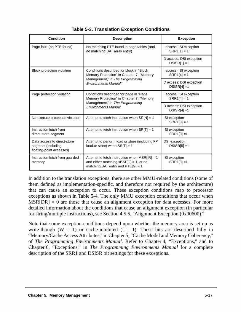
e ofcture)cessorhenmore
icular
t up asincy,”
o
In addition to the translation exceptions, there are other MMU-related conditions (somthem defined as implementation-specific, and therefore not required by the architethat can cause an exception to occur. These exception conditions map to proexceptions as shown in Table 5-4. The only MMU exception conditions that occur wMSR[DR] = 0 are those that cause an alignment exception for data accesses. Fordetailed information about the conditions that cause an alignment exception (in partfor string/multiple instructions), see Section 4.5.6, “Alignment Exception (0x00600).”
Note that some exception conditions depend upon whether the memory area is sewrite-though (W = 1) or cache-inhibited (I = 1). These bits are described fully“Memory/Cache Access Attributes,” in Chapter 5, “Cache Model and Memory Coherenof The Programming Environments Manual.Refer to Chapter 4, “Exceptions,” and tChapter 6, “Exceptions,” inThe Programming Environments Manualfor a completedescription of the SRR1 and DSISR bit settings for these exceptions.
Table 5-3. Translation Exception Conditions
Condition Description Exception
Page fault (no PTE found) No matching PTE found in page tables (andno matching BAT array entry)
I access: ISI exceptionSRR1[1] = 1
D access: DSI exceptionDSISR[1] =1
Block protection violation Conditions described for block in “BlockMemory Protection” in Chapter 7, “MemoryManagement,” in The ProgrammingEnvironments Manual.“
I access: ISI exceptionSRR1[4] = 1
D access: DSI exceptionDSISR[4] =1
Page protection violation Conditions described for page in “PageMemory Protection” in Chapter 7, “MemoryManagement,” in The ProgrammingEnvironments Manual.
I access: ISI exceptionSRR1[4] = 1
D access: DSI exceptionDSISR[4] =1
No-execute protection violation Attempt to fetch instruction when SR[N] = 1 ISI exceptionSRR1[3] = 1
Instruction fetch fromdirect-store segment
Attempt to fetch instruction when SR[T] = 1 ISI exceptionSRR1[3] =1
Data access to direct-storesegment (includingfloating-point accesses)
Attempt to perform load or store (including FPload or store) when SR[T] = 1
DSI exceptionDSISR[5] =1
Instruction fetch from guardedmemory
Attempt to fetch instruction when MSR[IR] = 1and either matching xBAT[G] = 1, or nomatching BAT entry and PTE[G] = 1
ISI exceptionSRR1[3] =1
Chapter 5. Memory Management 5-17

dress
er tothe pageween. Whenof thethe
ndedroutines
5.1.8 MMU Instructions and Register SummaryThe MMU instructions and registers allow the operating system to set up the block adtranslation areas and the page tables in memory.
Note that because the implementation of TLBs is optional, the instructions that refthese structures are also optional. However, as these structures serve as caches oftable, the architecture specifies a software protocol for maintaining coherency betthese caches and the tables in memory whenever the tables in memory are modifiedthe tables in memory are changed, the operating system purges these cachescorresponding entries, allowing the translation caching mechanism to refetch fromtables when the corresponding entries are required.
Note that the 750 implements all TLB-related instructions excepttlbia , which is treated asan illegal instruction.
Because the MMU specification for PowerPC processors is so flexible, it is recommethat the software that uses these instructions and registers be encapsulated into subto minimize the impact of migrating across the family of implementations.
Table 5-4. Other MMU Exception Conditions for the PowerPC 750 Processor
Condition Description Exception
dcbz with W = 1 or I = 1 dcbz instruction to write-through orcache-inhibited segment or block
Alignment exception (notrequired by architecture forthis condition)
lwarx or stwcx. with W = 1 Reservation instruction to write-throughsegment or block
DSI exceptionDSISR[5] =1
lwarx , stwcx. , eciwx , or ecowxinstruction to direct-store segment
Reservation instruction or external controlinstruction when SR[T] =1
DSI exceptionDSISR[5] =1
Floating-point load or store todirect-store segment
FP memory access when SR[T] =1 See data access todirect-store segment inTable 5-3.
Load or store that results in adirect-store error
Does not occur in 750 Does not apply
eciwx or ecowx attempted whenexternal control facility disabled
eciwx or ecowx attempted with EAR[E] = 0 DSI exceptionDSISR[11] = 1
lmw , stmw , lswi , lswx , stswi , orstswx instruction attempted inlittle-endian mode
lmw , stmw , lswi , lswx , stswi , or stswxinstruction attempted while MSR[LE] = 1
Alignment exception
Operand misalignment Translation enabled and a floating-pointload/store, stmw , stwcx. , lmw , lwarx , eciwx ,or ecowx instruction operand is notword-aligned
Alignment exception (someof these cases areimplementation-specific)
5-18 IBM PowerPC 740 / PowerPC 750 RISC Microprocessor User’s Manual
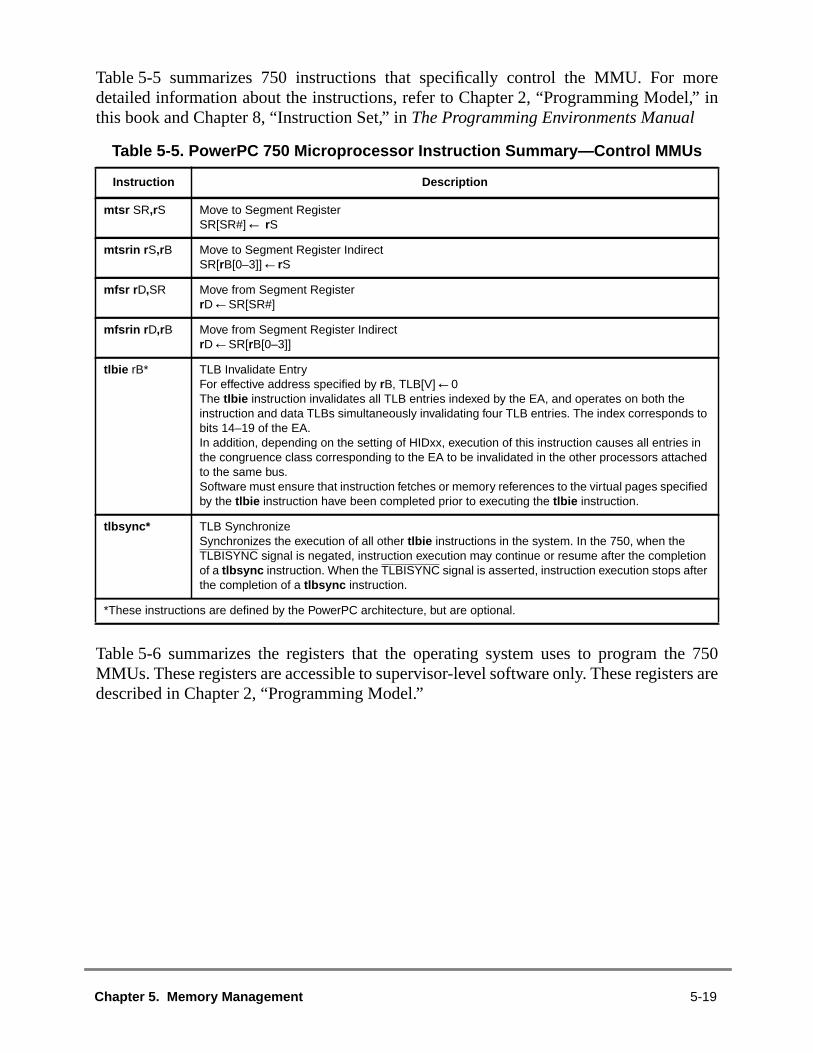
orel,” in
e 750ers are
Table 5-5 summarizes 750 instructions that specifically control the MMU. For mdetailed information about the instructions, refer to Chapter 2, “Programming Modethis book and Chapter 8, “Instruction Set,” inThe Programming Environments Manual
Table 5-6 summarizes the registers that the operating system uses to program thMMUs. These registers are accessible to supervisor-level software only. These registdescribed in Chapter 2, “Programming Model.”
Table 5-5. PowerPC 750 Microprocessor Instruction Summary—Control MMUs
Instruction Description
mtsr SR,rS Move to Segment RegisterSR[SR#]← rS
mtsrin r S,rB Move to Segment Register IndirectSR[rB[0–3]]←rS
mfsr r D,SR Move from Segment RegisterrD←SR[SR#]
mfsrin r D,rB Move from Segment Register IndirectrD←SR[rB[0–3]]
tlbie rB* TLB Invalidate EntryFor effective address specified by rB, TLB[V]←0The tlbie instruction invalidates all TLB entries indexed by the EA, and operates on both theinstruction and data TLBs simultaneously invalidating four TLB entries. The index corresponds tobits 14–19 of the EA.In addition, depending on the setting of HIDxx, execution of this instruction causes all entries inthe congruence class corresponding to the EA to be invalidated in the other processors attachedto the same bus.Software must ensure that instruction fetches or memory references to the virtual pages specifiedby the tlbie instruction have been completed prior to executing the tlbie instruction.
tlbsync* TLB SynchronizeSynchronizes the execution of all other tlbie instructions in the system. In the 750, when theTLBISYNC signal is negated, instruction execution may continue or resume after the completionof a tlbsync instruction. When the TLBISYNC signal is asserted, instruction execution stops afterthe completion of a tlbsync instruction.
*These instructions are defined by the PowerPC architecture, but are optional.
Chapter 5. Memory Management 5-19

ess,emory
heablehe dataloadust beset to
memoryideredideredhard
andnd” in
5.2 Real Addressing ModeIf address translation is disabled (MSR[IR] = 0 or MSR[DR] = 0) for a particular accthe effective address is treated as the physical address and is passed directly to the msubsystem as described in Chapter 7, “Memory Management,” inThe ProgrammingEnvironments Manual.
Note that the default WIMG bits (0b0011) cause data accesses to be considered cac(I = 0) and thus load and store accesses are weakly ordered. This is the case even if tcache is disabled in the HID0 register (as it is out of hard reset). If I/O devices requireand store accesses to occur in strict program order (strongly ordered), translation menabled so that the corresponding I bit can be set. Note also, that the G bit must beensure that the accesses are strongly ordered. For instruction accesses, the defaultaccess mode bits (WIMG) are also 0b0011. That is, instruction accesses are conscacheable (I = 0), and the memory is guarded. Again, instruction accesses are conscacheable even if the instruction cache is disabled in the HID0 register (as it is out ofreset). The W and M bits have no effect on the instruction cache.
For information on the synchronization requirements for changes to MSR[IR]MSR[DR], refer to Section 2.3.2.4, “Synchronization,” in this manual, a“Synchronization Requirements for Special Registers and for Lookaside BuffersChapter 2, “PowerPC Register Set,” inThe Programming Environments Manual.
Table 5-6. PowerPC 750 Microprocessor MMU Registers
Register Description
Segment registers(SR0–SR15)
The sixteen 32-bit segment registers are present only in 32-bit implementations ofthe PowerPC architecture. The fields in the segment register are interpreteddifferently depending on the value of bit 0. The segment registers are accessed bythe mtsr , mtsrin , mfsr , and mfsrin instructions.
BAT registers(IBAT0U–IBAT3U,IBAT0L–IBAT3L,DBAT0U–DBAT3U, andDBAT0L–DBAT3L)
There are 16 BAT registers, organized as four pairs of instruction BAT registers(IBAT0U–IBAT3U paired with IBAT0L–IBAT3L) and four pairs of data BAT registers(DBAT0U–DBAT3U paired with DBAT0L–DBAT3L). The BAT registers are defined as32-bit registers in 32-bit implementations. These are special-purpose registers thatare accessed by the mtspr and mfspr instructions.
SDR1 The SDR1 register specifies the variables used in accessing the page tables inmemory. SDR1 is defined as a 32-bit register for 32-bit implementations. Thisspecial-purpose register is accessed by the mtspr and mfspr instructions.
5-20 IBM PowerPC 740 / PowerPC 750 RISC Microprocessor User’s Manual

ngesmory.dlingerical
t,” in
theBATsether
hile
mory
ntedbyte
ming
address.” If
ntitye byte
A that
page.ystemmoryd and
5.3 Block Address TranslationThe block address translation (BAT) mechanism in the OEA provides a way to map raof effective addresses larger than a single page into contiguous areas of physical meSuch areas can be used for data that is not subject to normal virtual memory han(paging), such as a memory-mapped display buffer or an extremely large array of numdata.
Block address translation in the 750 is described in Chapter 7, “Memory ManagemenThe Programming Environments Manualfor 32-bit implementations.
Implementation Note—The 750 BAT registers are not initialized by the hardware afterpower-up or reset sequence. Consequently, all valid bits in both instruction and datamust be cleared before setting any BAT for the first time. This is true regardless of whaddress translation is enabled. Also, software must avoid overlapping blocks wupdating a BAT or areas.Even if translation is disabled, multiple BAT hits are treatedas programming errors and can corrupt the BAT registers and produce unpredictableresults. Always re-zero during the reset ISR. After zeroing all BATs, set them (inorder) to the desired values.HRESET disorders the BATs.SRESET does not.
5.4 Memory Segment ModelThe 750 adheres to the memory segment model as defined in Chapter 7, “MeManagement,” inThe Programming Environments Manualfor 32-bit implementations.Memory in the PowerPC OEA is divided into 256-Mbyte segments. This segmememory model provides a way to map 4-Kbyte pages of effective addresses to 4-Kpages in physical memory (page address translation), while providing the programflexibility afforded by a large virtual address space (52 bits).
The segment/page address translation mechanism may be superseded by the blocktranslation (BAT) mechanism described in Section 5.3, “Block Address Translationnot, the translation proceeds in the following two steps:
1. from effective address to the virtual address (which never exists as a specific ebut can be considered to be the concatenation of the virtual page number and thoffset within a page), and
2. from virtual address to physical address.
This section highlights those areas of the memory segment model defined by the OEare specific to the 750.
5.4.1 Page History RecordingReferenced (R) and changed (C) bits in each PTE keep history information about theThey are maintained by a combination of the 750 table search hardware and the ssoftware. The operating system uses this information to determine which areas of meto write back to disk when new pages must be allocated in main memory. Reference
Chapter 5. Memory Management 5-21

ion andnd toesses
. Theed on
it) isset in
its inages
orted as
bits.
ed as ifit in theey are
abled).
pagein theettingse theit in alls the
changed recording is performed only for accesses made with page address translatnot for translations made with the BAT mechanism or for accesses that correspodirect-store (T = 1) segments. Furthermore, R and C bits are maintained only for accmade while address translation is enabled (MSR[IR] = 1 or MSR[DR] = 1).
In the 750, the referenced and changed bits are updated as follows:
• For TLB hits, the C bit is updated according to Table 5-7.
• For TLB misses, when a table search operation is in progress to locate a PTER and C bits are updated (set, if required) to reflect the status of the page basthis access.
The table shows that the status of the C bit in the TLB entry (in the case of a TLB hwhat causes the processor to update the C bit in the PTE (the R bit is assumed to bethe page tables if there is a TLB hit). Therefore, when software clears the R and C bthe page tables in memory, it must invalidate the TLB entries associated with the pwhose referenced and changed bits were cleared.
Thedcbt anddcbtst instructions can execute if there is a TLB/BAT hit or if the processis in real addressing mode. In case of a TLB or BAT miss, these instructions are treano-ops; they do not initiate a table search operation and they do not set either the R or C
As defined by the PowerPC architecture, the referenced and changed bits are updataddress translation were disabled (real addressing mode). If these update accesses hdata cache, they are not seen on the external bus. If they miss in the data cache, thperformed as typical cache line fill accesses on bus (assuming the data cache is en
5.4.1.1 Referenced BitThe referenced (R) bit of a page is located in the PTE in the page table. Every time ais referenced (with a read or write access) and the R bit is zero, the 750 sets the R bitpage table. The OEA specifies that the referenced bit may be set immediately, or the smay be delayed until the memory access is determined to be successful. Becaureference to a page is what causes a PTE to be loaded into the TLB, the referenced b750 TLB entries is effectively always set. The processor never automatically clearreferenced bit.
Table 5-7. Table Search Operations to Update History Bits—TLB Hit Case
R and C bitsin TLB Entry
Processor Action
00 Combination doesn’t occur
01 Combination doesn’t occur
10 Read: No special actionWrite: The 750 initiates a table search operation to update C.
11 No special action for read or write
5-22 IBM PowerPC 740 / PowerPC 750 RISC Microprocessor User’s Manual

e. Atby thehis in
a
of thetore
esultsnot
et theh the
storeanteed
to be
th is
tore is
d bynarios,allows
ts are
The referenced bit is only a hint to the operating system about the activity of a pagtimes, the referenced bit may be set although the access was not logically requiredprogram or even if the access was prevented by memory protection. Examples of tPowerPC systems include the following:
• Fetching of instructions not subsequently executed
• A memory reference caused by a speculatively executed instruction that ismispredicted
• Accesses generated by anlswx or stswx instruction with a zero length
• Accesses generated by anstwcx. instruction when no store is performed becausereservation does not exist
• Accesses that cause exceptions and are not completed
5.4.1.2 Changed BitThe changed bit of a page is located both in the PTE in the page table and in the copyPTE loaded into the TLB (if a TLB is implemented, as in the 750). Whenever a data sinstruction is executed successfully, if the TLB search (for page address translation) rin a hit, the changed bit in the matching TLB entry is checked. If it is already set, it isupdated. If the TLB changed bit is 0, the 750 initiates the table search operation to sC bit in the corresponding PTE in the page table. The 750 then reloads the TLB (witC bit set).
The changed bit (in both the TLB and the PTE in the page tables) is set only when aoperation is allowed by the page memory protection mechanism and the store is guarto be in the execution path (unless an exception, other than those caused by thesc, rfi , ortrap instructions, occurs). Furthermore, the following conditions may cause the C bitset:
• The execution of an stwcx. instruction is allowed by the memory protectionmechanism but a store operation is not performed.
• The execution of anstswx instruction is allowed by the memory protectionmechanism but a store operation is not performed because the specified lengzero.
• The store operation is not performed because an exception occurs before the sperformed.
Again, note that although the execution of thedcbt anddcbtst instructions may cause theR bit to be set, they never cause the C bit to be set.
5.4.1.3 Scenarios for Referenced and Changed Bit RecordingThis section provides a summary of the model (defined by the OEA) that is usePowerPC processors for maintaining the referenced and changed bits. In some scethe bits are guaranteed to be set by the processor, in some scenarios, the architecturethat the bits may be set (not absolutely required), and in some scenarios, the bi
Chapter 5. Memory Management 5-23

ry, thele
triesrringbottomis
e that
respectted bythat
guaranteed to not be set. Note that when the 750 updates the R and C bits in memoaccesses are performed as if MSR[DR] = 0 and G = 0(that is, as nonguarded cacheaboperations in which coherency is required).
Table 5-8 defines a prioritized list of the R and C bit settings for all scenarios. The enin the table are prioritized from top to bottom, such that a matching scenario occucloser to the top of the table takes precedence over a matching scenario closer to theof the table. For example, if anstwcx. instruction causes a protection violation and thereno reservation, the C bit is not altered, as shown for the protection violation case. Notin the table, load operations include those generated by load instructions, by theeciwxinstruction, and by the cache management instructions that are treated as a load withto address translation. Similarly, store operations include those operations generastore instructions, by theecowxinstruction, and by the cache management instructionsare treated as a store with respect to address translation.
Table 5-8. Model for Guaranteed R and C Bit Settings
Priority Scenario
Causes Setting of R Bit Causes Setting of C Bit
OEAPowerPC
750OEA
PowerPC750
1 No-execute protection violation No No No No
2 Page protection violation Maybe Yes No No
3 Out-of-order instruction fetch or load operation Maybe No No No
4 Out-of-order store operation. Would be requiredby the sequential execution model in the absenceof system-caused or imprecise exceptions, or offloating-point assist exception for instructions thatwould cause no other kind of precise exception.
Maybe1 No No No
5 All other out-of-order store operations Maybe1 No Maybe1 No
6 Zero-length load (lswx ) Maybe No No No
7 Zero-length store (stswx ) Maybe1 No Maybe1 No
8 Store conditional (stwcx. ) that does not store Maybe1 Yes Maybe1 Yes
9 In-order instruction fetch Yes2 Yes No No
10 Load instruction or eciwx Yes Yes No No
11 Store instruction, ecowx or dcbz instruction Yes Yes Yes Yes
12 icbi , dcbt , or dcbtst instruction Maybe No No No
13 dcbst or dcbf instruction Maybe Yes No No
14 dcbi instruction Maybe1 Yes Maybe1 Yes
Notes :1 If C is set, R is guaranteed to be set also.2 Includes the case in which the instruction is fetched out of order and R is not set (does not apply for 750).
5-24 IBM PowerPC 740 / PowerPC 750 RISC Microprocessor User’s Manual

ory
ory
mizecilitate
nots not
theMU toset ofsters,ent
ets asressto a
40-bitTLB
For more information, see “Page History Recording” in Chapter 7, “MemManagement,” ofThe Programming Environments Manual.
5.4.2 Page Memory ProtectionThe 750 implements page memory protection as it is defined in Chapter 7, “MemManagement,” inThe Programming Environments Manual.
5.4.3 TLB DescriptionThe 750 implements separate 128-entry data and instruction TLBs to maxiperformance. This section describes the hardware resources provided in the 750 to fapage address translation. Note that the hardware implementation of the MMU isspecified by the architecture, and while this description applies to the 750, it doenecessarily apply to other PowerPC processors.
5.4.3.1 TLB OrganizationBecause the 750 has two MMUs (IMMU and DMMU) that operate in parallel, some ofMMU resources are shared, and some are actually duplicated (shadowed) in each Mmaximize performance. For example, although the architecture defines a singlesegment registers for the MMU, the 750 maintains two identical sets of segment regione for the IMMU and one for the DMMU; when an instruction that updates the segmregister executes, the 750 automatically updates both sets.
Each TLB contains 128 entries organized as a two-way set-associative array with 64 sshown in Figure 5-7 for the DTLB (the ITLB organization is the same). When an addis being translated, a set of two TLB entries is indexed in parallel with the accesssegment register. If the address in one of the two TLB entries is valid and matches thevirtual page number, that TLB entry contains the translation. If no match is found, amiss occurs.
Chapter 5. Memory Management 5-25

erationion isorder.y theagain,
bits
Figure 5-7. Segment Register and DTLB Organization
Unless the access is the result of an out-of-order access, a hardware table search opbegins if there is a TLB miss. If the access is out of order, the table search operatpostponed until the access is required, at which point the access is no longer out ofWhen the matching PTE is found in memory, it is loaded into the TLB entry selected bleast-recently-used (LRU) replacement algorithm, and the translation process beginsthis time with a TLB hit.
To uniquely identify a TLB entry as the required PTE, the PTE also contains four moreof the page index, EA[0–13] (in addition to the API bits in of the PTE).
Software cannot access the TLB arrays directly, except to invalidate an entry with thetlbieinstruction.
T
0 7 8 31
0
15 T VSID
Segment Registers
VDTLB
0
63
V
EA[0–31]
EA[0–3]
EA[14–19]
VSID
Select
Compare
Compare
EA[4–13]
Line 1
Line 0
MUX
RPNLine1/Line 0 Hit
PA[0–19]
5-26 IBM PowerPC 740 / PowerPC 750 RISC Microprocessor User’s Manual

d anye first
rs andrted atto bewhening,”tions.
opriatedressthenmberB
theseitiatedemory
triesstemessnd so
ing PTE.
any
the
ered,LBs,each
Each set of TLB entries has one associated LRU bit. The LRU bit for a set is updatetime either entry is used, even if the access is speculative. Invalid entries are always thto be replaced.
Although both MMUs can be accessed simultaneously (both sets of segment registeTLBs can be accessed in the same clock), only one exception condition can be repoa time. ITLB miss exceptions are reported when there are no more instructionsdispatched or retired (the pipeline is empty), and DTLB miss conditions are reportedthe load or store instruction is ready to be retired. Refer to Chapter 6, “Instruction Timfor more detailed information about the internal pipelines and the reporting of excep
When an instruction or data access occurs, the effective address is routed to the apprMMU. EA0–EA3 select one of the 16 segment registers and the remaining effective adbits and the VSID field from the segment register is passed to the TLB. EA[14–19]select two entries in the TLB; the valid bits are checked and the 40-bit virtual page nu(24-bit VSID and EA4–EA19]) must match the VSID, EAPI, and API fields of the TLentries. If one of the entries hits, the PP bits are checked for a protection violation. Ifbits don’t cause an exception, the C bit is checked and a table search operation is inif C must be updated. If C does not require updating, the RPN value is passed to the msubsystem and the WIMG bits are then used as attributes for the access.
Although address translation is disabled on a reset condition, the valid bits of TLB enare not automatically cleared. Thus, TLB entries must be explicitly cleared by the sysoftware (with thetlbie instruction) before the valid entries are loaded and addrtranslation is enabled. Also, note that the segment registers do not have a valid bit, athey should also be initialized before translation is enabled.
5.4.3.2 TLB InvalidationThe 750 implements the optionaltlbie and tlbsync instructions, which are used toinvalidate TLB entries. The execution of thetlbie instruction always invalidates fourentries—both the ITLB and DTLB entries indexed by EA[14–19].
The architecture allowstlbie to optionally enable a TLB invalidate signaling mechanismhardware so that other processors also invalidate their resident copies of the matchinThe 750 does not signal the TLB invalidation to other processors nor does it performaction when a TLB invalidation is performed by another processor.
The tlbsync instruction causes instruction execution to stop if theTLBISYNC signal isasserted. IfTLBISYNC is negated, instruction execution may continue or resume aftercompletion of atlbsync instruction. Section 8.8.2, “TLBISYNC Input,” describes the TLBsynchronization mechanism in further detail.
The tlbia instruction is not implemented on the 750 and when its opcode is encountan illegal instruction program exception is generated. To invalidate all entries of both T64 tlbie instructions must be executed, incrementing the value in EA14–EA19 by one
Chapter 5. Memory Management 5-27

pages
does
andsfin the
ents is
time. See Chapter 8, “Instruction Set,” inThe Programming Environments Manualfordetailed information about thetlbie instruction.
Software must ensure that instruction fetches or memory references to the virtualspecified by thetlbie have been completed prior to executing thetlbie instruction.
Other than the possible TLB miss on the next instruction prefetch, thetlbie instruction doesnot affect the instruction fetch operation—that is, the prefetch buffer is not purged andnot cause these instructions to be refetched.
5.4.4 Page Address Translation SummaryFigure 5-8 provides the detailed flow for the page address translation mechanism.
The figure includes the checking of the N bit in the segment descriptor and then expon the ‘TLB Hit’ branch of Figure 5-6. The detailed flow for the ‘TLB Miss’ branch oFigure 5-6 is described in Section 5.4.5, “Page Table Search Operation.” Note that ascase of block address translation, if an attempt is made to execute adcbz instruction to apage marked either write-through or caching-inhibited (W = 1 or I = 1), an alignmexception is generated. The checking of memory protection violation conditiondescribed in Chapter 7, “Memory Management,” inThe Programming EnvironmentsManual.
5-28 IBM PowerPC 740 / PowerPC 750 RISC Microprocessor User’s Manual
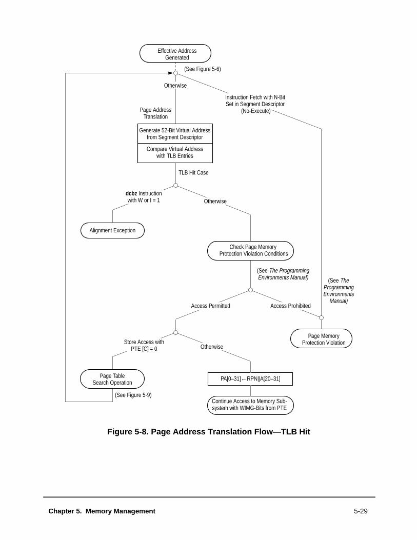
Figure 5-8. Page Address Translation Flow—TLB Hit
(See TheProgrammingEnvironments
Manual)
(See Figure 5-9)
(See The ProgrammingEnvironments Manual)
TLB Hit Case
Alignment Exception
Effective AddressGenerated
Continue Access to Memory Sub-system with WIMG-Bits from PTE
Page TableSearch Operation
PA[0–31]←RPN||A[20–31]
Page AddressTranslation
Check Page Memory Protection Violation Conditions
Instruction Fetch with N-BitSet in Segment Descriptor
(No-Execute)
Page MemoryProtection Violation
Access Permitted
OtherwiseStore Access with
PTE [C] = 0
Otherwisedcbz Instructionwith W or I = 1
Otherwise
(See Figure 5-6)
Generate 52-Bit Virtual Addressfrom Segment Descriptor
Compare Virtual Addresswith TLB Entries
Access Prohibited
Chapter 5. Memory Management 5-29
archrmat
Page
ccurre,he
ber field
theribed
ress
ause into
page:
the
5.4.5 Page Table Search OperationIf the translation is not found in the TLBs (a TLB miss), the 750 initiates a table seoperation which is described in this section. Formats for the PTE are given in “PTE Fofor 32-Bit Implementations,” in Chapter 7, “Memory Management,” ofThe ProgrammingEnvironments Manual.
The following is a summary of the page table search process performed by the 750:
1. The 32-bit physical address of the primary PTEG is generated as described in “Table Addresses” in Chapter 7, “Memory Management,” ofThe ProgrammingEnvironments Manual.
2. The first PTE (PTE0) in the primary PTEG is read from memory. PTE reads owith an implied WIM memory/cache mode control bit setting of 0b001. Therefothey are considered cacheable and read (burst) from memory and placed in tcache.
3. The PTE in the selected PTEG is tested for a match with the virtual page num(VPN) of the access. The VPN is the VSID concatenated with the page indexof the virtual address. For a match to occur, the following must be true:
— PTE[H] = 0— PTE[V] = 1— PTE[VSID] = VA[0–23]— PTE[API] = VA[24–29]
4. If a match is not found, step 3 is repeated for each of the other seven PTEs inprimary PTEG. If a match is found, the table search process continues as descin step 8. If a match is not found within the 8 PTEs of the primary PTEG, the addof the secondary PTEG is generated.
5. The first PTE (PTE0) in the secondary PTEG is read from memory. Again, becPTE reads have a WIM bit combination of 0b001, an entire cache line is readthe on-chip cache.
6. The PTE in the selected secondary PTEG is tested for a match with the virtualnumber (VPN) of the access. For a match to occur, the following must be true
— PTE[H] = 1— PTE[V] = 1— PTE[VSID] = VA[0–23]— PTE[API] = VA[24–29]
7. If a match is not found, step 6 is repeated for each of the other seven PTEs insecondary PTEG. If it is never found, an exception is taken (step 9).
5-30 IBM PowerPC 740 / PowerPC 750 RISC Microprocessor User’s Manual

tedthele
fails,
ndary
ded oron is
8. If a match is found, the PTE is written into the on-chip TLB and the R bit is updain the PTE in memory (if necessary). If there is no memory protection violation,C bit is also updated in memory (if the access is a write operation) and the tabsearch is complete.
9. If a match is not found within the 8 PTEs of the secondary PTEG, the search and a page fault exception condition occurs (either an ISI exception or a DSIexception).
Figure 5-9 and Figure 5-10 show how the conceptual model for the primary and secopage table search operations, described inThe Programming Environments Manual, arerealized in the 750.
Figure 5-9 shows the case of adcbz instruction that is executed with W = 1 or I = 1, anthat the R bit may be updated in memory (if required) before the operation is performthe alignment exception occurs. The R bit may also be updated if memory protectiviolated.
Chapter 5. Memory Management 5-31

Figure 5-9. Primary Page Table Search
(From Figure 5-10)
Fetch PTE from PTEG
Otherwise
Perform SecondaryPage Table Search
Alignment ExceptionTLB[PTE[C]] ← 1
Generate PA Using Primary Hash FunctionPA ← Base PA of PTEG
PA ← PA+ 8(Fetch Next PTE in PTEG)
Fetch PTE (64-Bits)from PA
PTE [VSID, API, H, V] =Segment Descriptor [VSID], EA[API], 0, 1
PTE[C] ←1(Update PTE[C] in Memory)
Also Update PTE[R]in Memory if R_Flag = 1
PTE[R] ←1(Update PTE[R] in
Memory)
Last PTE in PTEG PTE[R] = 0
R_Flag = 1
Store Operationwith PTE[C] = 0
Otherwise
R_Flag = 1
PTE[R] ←1 (UpdatePTE[R] in Memory)
Primary PageTable Search
Write PTE intoTLB
Otherwise
Secondary Page TableSearch Hit
PTE[R] = 1
dcbz Instructionwith W or I = 1
Check Memory ProtectionViolation Conditions
R_Flag = 1
PTE[R] ←1(Update PTE[R]
in Memory)
Otherwise
PTE[R] ← 1R_Flag ← 1
Memory ProtectionViolation
Page TableSearch Complete
Page TableSearch Complete
OtherwiseOtherwise
Access PermittedAccess Prohibited
Otherwise
5-32 IBM PowerPC 740 / PowerPC 750 RISC Microprocessor User’s Manual

o so.til theetectsd by
ated
MUlizesuencerd, the
ever,g asns can
Figure 5-10. Secondary Page Table Search Flow
The LSU initiates out-of-order accesses without knowledge of whether it is legal to dTherefore, the MMU does not perform hardware table search due to TLB misses unrequest is required by the program flow. In these out-of-order cases, the MMU does dprotection violations and whether adcbz instruction specifies a page marked awrite-through or cache-inhibited. The MMU also detects alignment exceptions causethe dcbz instruction and prevents the changed bit in the PTE from being upderroneously in these cases.
If an MMU register is being accessed by an instruction in the instruction stream, the IMstalls for one translation cycle to perform that operation. The sequencer seriainstructions to ensure the data correctness. For updating the IBATs and SRs, the seqclassifies those operations as fetch serializing. After such an instruction is dispatcheinstruction buffer is flushed and the fetch stalls until the instruction completes. Howfor reading from the IBATs, the operation is classified as execution serializing. As lonthe LSU ensures that all previous instructions can be executed, subsequent instructiobe fetched and dispatched.
Page Fault (See Figure 5-9)
Fetch PTE from PTEG
Otherwise
Generate PA Using Primary Hash FunctionPA ← Base PA of PTEG
PA ← PA+ 8(Fetch Next PTE in PTEG)
Fetch PTE (64-Bits)from PA
PTE [VSID, API, H, V] =Segment Descriptor [VSID], EA[API], 1, 1
Last PTE in PTEG
Secondary PageTable Search
Otherwise
Secondary Page TableSearch Hit
ISI Exception DSI Exception
Set SRR1[1] = 1 Set DSISR[1] = 1
Instruction Access Data Access
Chapter 5. Memory Management 5-33

of thetry
dedeen
TLB
storeefore,.
ive orind ofd annot beet,” int
s areside
5.4.6 Page Table UpdatesWhen TLBs are implemented (as in the 750) they are defined as noncoherent cachespage tables. TLB entries must be flushed explicitly with the TLB invalidate eninstruction (tlbie) whenever the corresponding PTE is modified. As the 750 is intenprimarily for uniprocessor environments, it does not provide coherency of TLBs betwmultiple processors. If the 750 is used in a multiprocessor environment wherecoherency is required, all synchronization must be implemented in software.
Processors may write referenced and changed bits with unsynchronized, atomic byteoperations. Note that the V, R, and C bits each reside in a distinct byte of a PTE. Therextreme care must be taken to use byte writes when updating only one of these bits
Explicitly altering certain MSR bits (using themtmsr instruction), or explicitly alteringPTEs, or certain system registers, may have the side effect of changing the effectphysical addresses from which the current instruction stream is being fetched. This kside effect is defined as an implicit branch. Implicit branches are not supported anattempt to perform one causes boundedly-undefined results. Therefore, PTEs mustchanged in a manner that causes an implicit branch. Chapter 2, “PowerPC Register SThe Programming Environments Manual, lists the possible implicit branch conditions thacan occur when system registers and MSR bits are changed.
5.4.7 Segment Register UpdatesSynchronization requirements for using the move to segment register instructiondescribed in “Synchronization Requirements for Special Registers and for LookaBuffers” in Chapter 2, “PowerPC Register Set,” inThe Programming EnvironmentsManual.
5-34 IBM PowerPC 740 / PowerPC 750 RISC Microprocessor User’s Manual

s, andtailedtheraches.
ow toach
ation
heset out
Suchoes
g.
n. Ation
heee
the
Chapter 6Instruction Timing6060
This chapter describes how the PowerPC 750 microprocessor fetches, dispatcheexecutes instructions and how it reports the results of instruction execution. It gives dedescriptions of how the 750 execution units work, and how those units interact with oparts of the processor, such as the instruction fetching mechanism, register files, and cIt gives examples of instruction sequences, showing potential bottlenecks and hminimize their effects. Finally, it includes tables that identify the unit that executes einstruction implemented on the 750, the latency for each instruction, and other informthat is useful for the assembly language programmer.
6.1 Terminology and ConventionsThis section provides an alphabetical glossary of terms used in this chapter. Tdefinitions are provided as a review of commonly used terms and as a way to poinspecific ways these terms are used in this chapter.
• Branch prediction—The process of guessing whether a branch will be taken. predictions can be correct or incorrect; the term ‘predicted’ as it is used here dnot imply that the prediction is correct (successful). The PowerPC architecturedefines a means for static branch prediction as part of the instruction encodin
• Branch resolution—The determination of whether a branch is taken or not takebranch is said to be resolved when the processor can determine which instrucpath to take. If the branch is resolved as predicted, the instructions following tpredicted branch that may have been speculatively executed can complete (scompletion). If the branch is not resolved as predicted, instructions on themispredicted path, and any results of speculative execution, are purged from pipeline and fetching continues from the nonpredicted path.
• Completion—Completion occurs when an instruction has finished executing,written back any results, and is removed from the completion queue. When aninstruction completes, it is guaranteed that this instruction and all previousinstructions can cause no exceptions.
Chapter 6. Instruction Timing 6-1

gh is,atchition
r
hher
ion
ake
areal is
omes
berthe) is
llows the
.
er thelatter
n, orlockrite-
stage.
• Fall-through (branch fall-through)—A not-taken branch. On the 750, fall-throubranch instructions are removed from the instruction stream at dispatch. Thatthese instructions are allowed to fall through the instruction queue via the dispmechanism, without either being passed to an execution unit and or given a posin the completion queue.
• Fetch—The process of bringing instructions from memory (such as a cache osystem memory) into the instruction queue.
• Folding (branch folding)—The replacement with target instructions of a brancinstruction and any instructions along the not-taken path when a branch is eittaken or predicted as taken.
• Finish—Finishing occurs in the last cycle of execution. In this cycle, the completqueue entry is updated to indicate that the instruction has finished executing.
• Latency— The number of clock cycles necessary to execute an instruction and mready the results of that execution for a subsequent instruction.
• Pipeline—In the context of instruction timing, the term ‘pipeline’ refers to theinterconnection of the stages. The events necessary to process an instructionbroken into several cycle-length tasks to allow work to be performed on severinstructions simultaneously—analogous to an assembly line. As an instructionprocessed, it passes from one stage to the next. When it does, the stage becavailable for the next instruction.
Although an individual instruction may take many cycles to complete (the numof cycles is called instruction latency), pipelining makes it possible to overlap processing so that the throughput (number of instructions completed per cyclegreater than if pipelining were not implemented.
• Program order—The order of instructions in an executing program. Morespecifically, this term is used to refer to the original order in which programinstructions are fetched into the instruction queue from the cache.
• Rename register—Temporary buffers used by instructions that have finishedexecution but have not completed.
• Reservation station—A buffer between the dispatch and execute stages that ainstructions to be dispatched even though the results of instructions on whichdispatched instruction may depend are not available.
• Retirement—Removal of the completed instruction from the completion queue
• Stage—The term ‘stage’ is used in two different senses, depending on whethpipeline is being discussed as a physical entity or a sequence of events. In thecase, a stage is an element in the pipeline during which certain actions areperformed, such as decoding the instruction, performing an arithmetic operatiowriting back the results. A stage is typically described as taking a processor ccycle to perform its operation; however, some events (such as dispatch and wback) happen instantaneously, and may be thought to occur at the end of the
6-2 IBM PowerPC 740 / PowerPC 750 RISC Microprocessor User’s Manual

quent
ously,ample,ueue
ccupy
ons
time.
ycle.s a
not
clockresultsaccess-backble orccessnother
esses.
scalarativeallel.
ctionveralr an
uction
An instruction can spend multiple cycles in one stage. An integer multiply, forexample, takes multiple cycles in the execute stage. When this occurs, subseinstructions may stall.
In some cases, an instruction may also occupy more than one stage simultaneespecially in the sense that a stage can be seen as a physical resource—for exwhen instructions are dispatched they are assigned a place in the completion qat the same time they are passed to the execute stage. They can be said to oboth the complete and execute stages in the same clock cycle.
• Stall—An occurrence when an instruction cannot proceed to the next stage.
• Superscalar—A superscalar processor is one that can issue multiple instructiconcurrently from a conventional linear instruction stream. In a superscalarimplementation, multiple instructions can be in the execute stage at the same
• Throughput—A measure of the number of instructions that are processed per cFor example, a series of double-precision floating-point multiply instructions hathroughput of one instruction per clock cycle.
• Write-back—Write-back (in the context of instruction handling) occurs when aresult is written into the architectural registers (typically the GPRs and FPRs).Results are written back at completion time. Results in the write-back buffer canbe flushed. If an exception occurs, these buffers must write back before theexception is taken.
6.2 Instruction Timing OverviewThe 750 design minimizes average instruction execution latency, the number ofcycles it takes to fetch, decode, dispatch, and execute instructions and make theavailable for a subsequent instruction. Some instructions, such as loads and stores,memory and require additional clock cycles between the execute phase and the writephase. These latencies vary depending on whether the access is to cacheanoncacheable memory, whether it hits in the L1 or L2 cache, whether the cache agenerates a write-back to memory, whether the access causes a snoop hit from adevice that generates additional activity, and other conditions that affect memory acc
The 750 implements many features to improve throughput, such as pipelining, superinstruction issue, branch folding, removal of fall-through branches, two-level speculbranch handling, and multiple execution units that operate independently and in par
As an instruction passes from stage to stage in a pipelined system, the following instrucan follow through the stages as the former instruction vacates them, allowing seinstructions to be processed simultaneously. While it may take several cycles foinstruction to pass through all the stages, when the pipeline has been filled, one instrcan complete its work on every clock cycle.
Chapter 6. Instruction Timing 6-3

plete,750’s
rallel:
ides
sseswn inr to
Figure 6-1 represents a generic pipelined execution unit.
Figure 6-1. Pipelined Execution Unit
The entire path that instructions take through the fetch, decode/dispatch, execute, comand write-back stages is considered the 750’s master pipeline, and two of theexecution units (the FPU and LSU) are also multiple-stage pipelines.
The 750 contains the following execution units that operate independently and in pa
• Branch processing unit (BPU)• Integer unit 1 (IU1)—executes all integer instructions• Integer unit 2 (IU2)—executes all integer instructions except multiplies and div• 64-bit floating-point unit (FPU)• Load/store unit (LSU)• System register unit (SRU)
The 750 can retire two instructions on every clock cycle. In general, the 750 proceinstructions in four stages—fetch, decode/dispatch, execute, and complete as shoFigure 6-2. Note that the example of a pipelined execution unit in Figure 6-1 is similathe three-stage FPU pipeline in Figure 6-2.
Clock 0
Clock 1
Clock 2
Clock 3
Instruction A — —
Instruction B
Instruction C
Instruction D
Instruction A
Instruction B
Instruction C
—
Instruction A
Instruction B
Stage 1 Stage 2 Stage 3
6-4 IBM PowerPC 740 / PowerPC 750 RISC Microprocessor User’s Manual

toch as
ry tokare
ion
ted.
ction
an
cle.
Figure 6-2. Superscalar/Pipeline Diagram
The instruction pipeline stages are described as follows:
• The instruction fetch stage includes the clock cycles necessary to requestinstructions from the memory system and the time the memory system takes respond to the request. Instruction fetch timing depends on many variables, suwhether the instruction is in the branch target instruction cache, the on-chipinstruction cache, or the L2 cache. Those factors increase when it is necessafetch instructions from system memory, and include the processor-to-bus clocratio, the amount of bus traffic, and whether any cache coherency operations required.
Because there are so many variables, unless otherwise specified, the instructtiming examples below assume optimal performance, that the instructions areavailable in the instruction queue in the same clock cycle that they are requesThe fetch stage ends when the instruction is dispatched.
• The decode/dispatch stage consists of the time it takes to fully decode the instruand dispatch it from the instruction queue to the appropriate execution unit.Instruction dispatch requires the following:
— Instructions can be dispatched only from the two lowest instruction queueentries, IQ0 and IQ1.
— A maximum of two instructions can be dispatched per clock cycle (althoughadditional branch instruction can be handled by the BPU).
— Only one instruction can be dispatched to each execution unit per clock cy
— There must be a vacancy in the specified execution unit.
Fetch
Complete (Write-back)
Decode/Dispatch
Execute Stage
FPU3SRU IU2IU1
Maximum three-instruction dispatchper clock cycle (includes one branchinstruction)
Maximum two -instructioncompletion per clock cycle
FPU2
FPU1
LSU1
Maximum four-instruction fetchper clock cycle
LSU2
BPU
Chapter 6. Instruction Timing 6-5

y the
able
t (orunit.
canver,heions
ropertus,ters
beeue
n iscanthecan
slationuallyhensix
ndcribe
etch
d bythein
— A rename register must be available for each destination operand specified binstruction.
— For an instruction to dispatch, the appropriate execution unit must be availand there must be an open position in the completion queue. If no entry isavailable, the instruction remains in the IQ.
• The execute stage consists of the time between dispatch to the execution unireservation station) and the point at which the instruction vacates the execution
Most integer instructions have a one-cycle latency; results of these instructionsbe used in the clock cycle after an instruction enters the execution unit. Howeinteger multiply and divide instructions take multiple clock cycles to complete. TIU1 can process all integer instructions; the IU2 can process all integer instructexcept multiply and divide instructions.
The LSU and FPU are pipelined (as shown in Figure 6-2).
• The complete (complete/write-back) pipeline stage maintains the correctarchitectural machine state and commits it to the architectural registers at the ptime. If the completion logic detects an instruction containing an exception staall following instructions are cancelled, their execution results in rename regisare discarded, and the correct instruction stream is fetched.
The complete stage ends when the instruction is retired. Two instructions canretired per cycle. Instructions are retired only from the two lowest completion quentries, CQ0 and CQ1.
The notation conventions used in the instruction timing examples are as follows:
Fetch—The fetch stage includes the time between when an instructiorequested and when it is brought into the instruction queue. This latencybe very variable, depending upon whether the instruction is in the BTIC,on-chip cache, the L2 cache, or system memory (in which case latencybe affected by bus speed and traffic on the system bus, and address tranissues). Therefore, in the examples in this chapters, the fetch stage is usidealized, that is, an instruction is usually shown to be in the fetch stage wit is a valid instruction in the instruction queue. The instruction queue hasentries, IQ0–IQ5.
In dispatch entry (IQ0/IQ1)—Instructions can be dispatched from IQ0 aIQ1. Because dispatch is instantaneous, it is perhaps more useful to desit as an event that marks the point in time between the last cycle in the fstage and the first cycle in the execute stage.
Execute—The operations specified by an instruction are being performethe appropriate execution unit. The black stripe is a reminder thatinstruction occupies an entry in the completion queue, describedFigure 6-3.
6-6 IBM PowerPC 740 / PowerPC 750 RISC Microprocessor User’s Manual

, then is
andend
to thetions
. Only
750re toes the
Complete—The instruction is in the completion queue. In the final stageresults of the executed instruction are written back and the instructioretired. The completion queue has six entries, CQ0–CQ5.
In retirement entry—Completed instructions can be retired from CQ0CQ1. Like dispatch, retirement is an event that in this case occurs at theof the final cycle of the complete stage.
Figure 6-3 shows the stages of 750 execution units.
Figure 6-3. PowerPC 750 Microprocessor Pipeline Stages
6.3 Timing ConsiderationsThe 750 is a superscalar processor; as many as three instructions can be issuedexecution units (one branch instruction to the branch processing unit, and two instrucissued from the dispatch queue to the other execution units) during each clock cycleone instruction can be dispatched to each execution unit.
Although instructions appear to the programmer to execute in program order, theimproves performance by executing multiple instructions at a time, using hardwamanage dependencies. When an instruction is dispatched, the register file provid
Fetch In Dispatch Execute1 Complete/Retire
Fetch In Dispatch Complete/RetireEA
Fetch In Dispatch Complete/Retire
IU1/IU2/SRU Instructions
LSU Instructions
FPU Instructions
NormalizeMultiply Add Round/
1 Several integer instructions, such as multiply and divide instructions, require multiple cycles in
Execute
Execute
CalculationCache Align
Entry
Entry
Entry
the execute stage.
BPU Instructions
Fetch FetchPredict
Complete/Retire2In DispatchEntry
In CompletionQueue2
2 Only those branch instructions that update the LR or CTR take an entry in the completion queue.
Chapter 6. Instruction Timing 6-7
ficient
hen arectionrrect,
wed
thet GPRsourcellowse datatheir
clockthe
ache
er ofles inons inallytchedTIC,nextthehip
achee byt.”
source data to the execution unit. The register files and rename register have sufbandwidth to allow dispatch of two instructions per clock under most conditions.
The 750’s BPU decodes and executes branches immediately after they are fetched. Wconditional branch cannot be resolved due to a CR data dependency, the branch diis predicted and execution continues from the predicted path. If the prediction is incothe following steps are taken:
1. The instruction queue is purged and fetching continues from the correct path.
2. Any instructions ahead of the predicted branch in the completion queue are alloto complete.
3. Instructions after the mispredicted branch are purged.
4. Dispatching resumes from the correct path.
After an execution unit finishes executing an instruction, it places resulting data intoappropriate GPR or FPR rename register. The results are then stored into the correcor FPR during the write-back stage. If a subsequent instruction needs the result as aoperand, it is made available simultaneously to the appropriate execution unit, which aa data-dependent instruction to be decoded and dispatched without waiting to read thfrom the register file. Branch instructions that update either the LR or CTR write backresults in a similar fashion.
The following section describes this process in greater detail.
6.3.1 General Instruction FlowAs many as four instructions can be fetched into the instruction queue (IQ) in a singlecycle. Instructions enter the IQ and are issued to the various execution units fromdispatch queue. The 750 tries to keep the IQ full at all times, unless instruction cthrottling is operating.
The number of instructions requested in a clock cycle is determined by the numbvacant spaces in the IQ during the previous clock cycle. This is shown in the exampthis chapter. Although the instruction queue can accept as many as four new instructia single clock cycle, if only one IQ entry is vacant, only one instruction is fetched. Typicinstructions are fetched from the on-chip instruction cache, but they may also be fefrom the branch target instruction cache (BTIC). If the instruction request hits in the Bit can usually present the first two instructions of the new instruction stream in theclock cycle, giving enough time for the next pair of instructions to be fetched frominstruction cache with no idle cycles. If instructions are not in the BTIC or the on-cinstruction cache, they are fetched from the L2 cache or from system memory.
The 750’s instruction cache throttling feature, managed through the instruction cthrottling control (ICTC) register, can lower the processor’s overall junction temperaturslowing the instruction fetch rate. See Chapter 10, “Power and Thermal Managemen
6-8 IBM PowerPC 740 / PowerPC 750 RISC Microprocessor User’s Manual

ctly,itionstion is, thequickions.
rget
reamn be
n orh
.3.1,
ctionribedns.”(evenosition
n theletions arene in
Branch instructions are identified by the fetcher, and forwarded to the BPU direbypassing the dispatch queue. If the branch is unconditional or if the specified condare already known, the branch can be resolved immediately. That is, the branch direcknown and instruction fetching can continue from the correct location. Otherwisebranch direction must be predicted. The 750 offers several resources to aid inresolution of branch instructions and for improving the accuracy of branch predictThese include the following:
• Branch target instruction cache—The 64-entry (four-way-associative) branch tainstruction cache (BTIC) holds branch target instructions so when a branch isencountered in a repeated loop, usually the first two instructions in the target stcan be fetched into the instruction queue on the next clock cycle. The BTIC cadisabled and invalidated through bits in HID0.
• Dynamic branch prediction—The 512-entry branch history table (BHT) isimplemented with two bits per entry for four degrees of prediction—not-taken,strongly not-taken, taken, strongly taken. Whether a branch instruction is takenot-taken can change the strength of the next prediction. This dynamic brancprediction is not defined by the PowerPC architecture.
To reduce aliasing, only predicted branches update the BHT entries. Dynamicbranch prediction is enabled by setting HID0[BHT]; otherwise, static branchprediction is used.
• Static branch prediction—Static branch prediction is defined by the PowerPCarchitecture and involves encoding the branch instructions. See Section 6.4.1“Static Branch Prediction.”
Branch instructions that do not update the LR or CTR are removed from the instrustream either by branch folding or removal of fall-through branch instructions, as descin Section 6.4.1.1, “Branch Folding and Removal of Fall-Through Branch InstructioBranch instructions that update the LR or CTR are treated as if they require dispatchthrough they are not issued to an execution unit in the process). They are assigned a pin the completion queue to ensure that the CTR and LR are updated sequentially.
All other instructions are issued from the IQ0 and IQ1. The dispatch rate depends upoavailability of resources such as the execution units, rename registers, and compqueue entries, and upon the serializing behavior of some instructions. Instructiondispatched in program order; an instruction in IQ1 cannot be dispatched ahead of oIQ0.
Chapter 6. Instruction Timing 6-9
Figure 6-4 shows the paths taken by instructions.
Figure 6-4. Instruction Flow Diagram
SRUIU2
FPU
Complete (Retire)
Fetch
LSU
DispatchBranch
Instruction Queue
Completion Queue
Completion Queue
IU1
Store Queue
Processing Unit
(In program order)
Assignment
(In program order)
CQ5 CQ4 CQ3 CQ2 CQ1 CQ0
IQ5 IQ4 IQ3 IQ2 IQ1 IQ0
(Maximum 2 instructions per clock cycle; 1 instruction per unit)
(Maximum four instructions per clock cycle)
ReservationStations
6-10 IBM PowerPC 740 / PowerPC 750 RISC Microprocessor User’s Manual

chipmorypeed,s.
hingst, theyto aletes.
thecaches). Thesting
che.t addhows are
lines
6.3.2 Instruction Fetch TimingInstruction fetch latency depends on whether the fetch hits the BTIC, the on-instruction cache, or the L2 cache, if one is implemented. If no cache hit occurs, a metransaction is required in which case fetch latency is affected by bus traffic, bus clock sand memory translation. These issues are discussed further in the following section
6.3.2.1 Cache ArbitrationWhen the instruction fetcher requests instructions from the instruction cache, two tmay happen. If the instruction cache is idle and the requested instructions are presenare provided on the next clock cycle. However, if the instruction cache is busy duecache-line-reload operation, instructions cannot be fetched until that operation comp
6.3.2.2 Cache HitIf the instruction fetch hits the instruction cache, it takes only one clock cycle afterrequest for as many as four instructions to enter the instruction queue. Note that theis not blocked to internal accesses during a cache reload completes (hits under missecritical double word is written simultaneously to the cache and forwarded to the requeunit, minimizing stalls due to load delays.
Figure 6-5 shows a simple example of instruction fetching that hits in the on-chip caThis example uses a series of integer add and double-precision floating-poininstructions to show how the number of instructions to be fetched is determined,program order is maintained by the instruction and completion queues, how instructiondispatched and retired in pairs (maximum), and how the FPU, IU1, and IU2 pipefunction. The following instruction sequence is examined:
3 add4 fadd5 add6 fadd7 br 68 fsub9 fadd10 fadd11 add12 add13 add14 add15 fadd16 add17 fadd18 .19 .20 .
Chapter 6. Instruction Timing 6-11

ande
Figure 6-5. Instruction Timing—Cache Hit
The instruction timing for this example is described cycle-by-cycle as follows:
0. In cycle 0, instructions 0–3 are fetched from the instruction cache. Instructions 01 are placed in the two entries in the instruction queue from which they can bdispatched on the next clock cycle.
6 fadd
1 fadd
0 add
10 11
8 add
1 2 3 4 5 6 7 80
Fetch (in IQ)
In dispatch entry (IQ0/IQ1)
Execute2 add
3 fadd
9 add
4 b
10 add
11 add
12 fadd
9
7 fadd
•••
Complete (In CQ)
13 add
14 fadd
3
2
1
0
7
6
11
10
9
8
7
12
11
10
9
8
7
12
11
10
9
14
13
12
11
(16)
(15)
14
13
(18)
(17)
(16)
(15)
14
13
(18)
(17)
(16)
(15)
5
4
3
2
3
2
1
0
6
3
2
1
6
3
2
1
8
7
6
3
10
9
8
7
6
12
11
10
9
8
7
12
11
10
9
8
7
14
13
12
11
10
9
14
13
12
11
14
13
1
0
InstructionQueue
CompletionQueue
5 fsub
In retirement entry (CQ0/CQ1)
6-12 IBM PowerPC 740 / PowerPC 750 RISC Microprocessor User’s Manual

ly.in thetionsdropwoandalit can
into
ue by,firsteitherded.
5 in
ction
, andcle
lock
ons
not betionone is
hes 9 arele 4.ute
IU1,
1. In cycle 1, instructions 0 and 1 are dispatched to the IU2 and FPU, respectiveNotice that for instructions to be dispatched they must be assigned positions completion queue. In this case, since the completion queue was empty, instruc0 and 1 take the two lowest entries in the completion queue. Instructions 2 and 3into the two dispatch positions in the instruction queue. Because there were tpositions available in the instruction queue in clock cycle 0, two instructions (45) are fetched into the instruction queue. Instruction 4 is a branch unconditioninstruction, which resolves immediately as taken. Because the branch is taken,therefore be folded from the instruction queue.
2. In cycle 2, assume a BTIC hit occurs and target instructions 6 and 7 are fetchedthe instruction queue, replacing the foldedb instruction (4) and instruction 5.Instruction 0 completes, writes back its results and vacates the completion quethe end of the clock cycle. Instruction 1 enters the second FPU execute stageinstruction 2 is dispatched to the IU2, and instruction 3 is dispatched into the FPU execute stage. Because the taken branch instruction (4) does not updateCTR or LR, it does not require a position in the completion queue and can be fol
3. In cycle 3, target instructions (6 and 7) are fetched, replacing instructions 4 andIQ0 and IQ1. This replacement on taken branches is called branch folding.Instruction 1 proceeds through the last of the three FPU execute stages. Instru2 has executed but must remain in the completion queue until instruction 1completes. Instruction 3 replaces instruction 1 in the second stage of the FPUinstruction 6 replaces instruction 3 in the first stage. Also, as will be shown in cy4, there is a single-cycle stall that occurs when the FPU pipeline is full.
Because there were three vacancies in the instruction queue in the previous ccycle, instructions 8–11 are fetched in this clock cycle.
4. Instruction 1 completes in cycle 4, allowing instruction 2 to complete. Instructi3 and 6 continue through the FPU pipeline. Although instruction 7 is in IQ1, itcannot be dispatched because the FPU is busy, and because instruction 7 candispatched neither can instruction 8. The additional cycle stall allows the instrucqueue to be completely filled. Because there was one opening in the instructiqueue in clock cycle 3, one instruction is fetched (12) and the instruction queufull.
5. In cycle 5, instruction 3 completes, allowing instruction 7 to be dispatched to tFPU, which in turn allows instruction 8 to be dispatched to the IU2. Instructionand 10 drop to the dispatch positions in the instruction queue. No instructionsfetched in this clock cycle because there were no vacant IQ entries in clock cyc
6. In cycle 6, instruction 6 completes, instruction 7 is in stage 2 of the FPU execstage, and although instruction 8 has executed, it must wait for instruction 7 tocomplete. The two integer instructions, 9 and 10, are dispatched to the IU2 andrespectively. Fetching resumes with instructions 13 and 14.
Chapter 6. Instruction Timing 6-13

waitFPU,
hed.lete,
s full,n
thection
he. Aas in
s notannot
stageuired
clockcyclerded
7. In cycle 7, instruction 7 is in the final FPU execute stage and instructions 8–10in the completion queue. Instructions 11 and 12 are dispatched to the IU2 andrespectively. Note that at this point the completion queue is full. Two moreinstructions (15 and 16, which are shown only in the instruction queue) are fetc
8. In cycle 8, instructions 7–11 are through executing. Instructions 7 and 8 compwrite back, and vacate the completion queue. Because the completion queue iinstructions 13 and 14 cannot be dispatched and must remain in the instructioqueue. Only the FPU is executing during this cycle (instruction 12). Additionalinstructions (instructions 16 and 17, shown only in the instruction queue) arefetched, filling the instruction queue.
9. In cycle 9, two more instructions (instructions 7 and 8) are retired from thecompletion queue allowing instructions 13 and 14 to be dispatched, again fillingcompletion queue. No instructions are fetched on this cycle because the instruqueue was full on the previous clock cycle.
6.3.2.3 Cache MissFigure 6-6 shows an instruction fetch that misses both the on-chip cache and L2 cacprocessor/bus clock ratio is 1:2 is used. The same instruction sequence is usedSection 6.3.2.2, “Cache Hit,” however in this example, the branch target instruction iin either the L1 or L2 cache. Because the target instruction is not in the L1 cache, it cbe in the BTIC.
A cache miss, extends the latency of the fetch stage, so in this example, the fetchshown represents not only the time the instruction spends in the IQ, but the time reqfor the instruction to be loaded from system memory, beginning in clock cycle 2.
During clock cycle 3, the target instruction for theb instruction is not in the BTIC, theinstruction cache or the L2 cache; therefore, a memory access must occur. Duringcycle 5, the address of the block of instructions is sent to the system bus. During clock7, two instructions (64 bits) are returned from memory on the first beat and are forwaboth to the cache and the instruction fetcher.
6-14 IBM PowerPC 740 / PowerPC 750 RISC Microprocessor User’s Manual
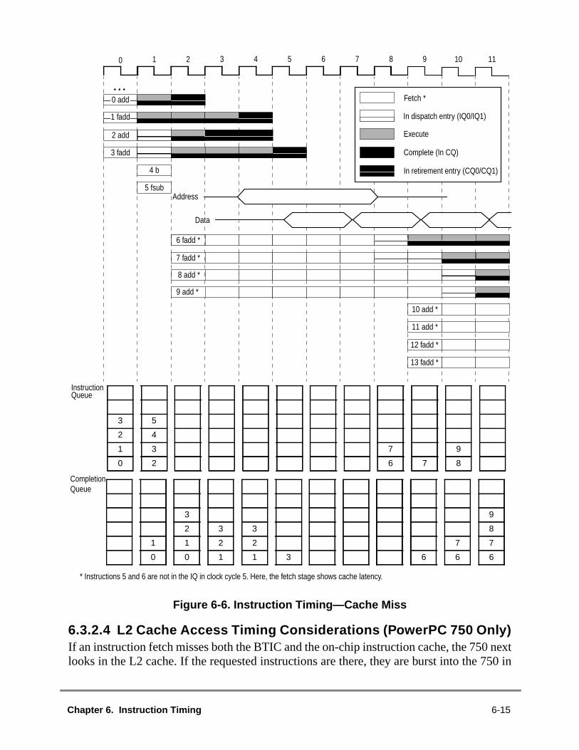
next50 in
Figure 6-6. Instruction Timing—Cache Miss
6.3.2.4 L2 Cache Access Timing Considerations (PowerPC 750 Only)If an instruction fetch misses both the BTIC and the on-chip instruction cache, the 750looks in the L2 cache. If the requested instructions are there, they are burst into the 7
6 fadd *
7 fadd *
1 fadd
0 add
10 11
8 add *
1 2 3 4 5 6 7 80
2 add
3 fadd
9 add *
4 b
10 add *
11 add *
12 fadd *
9
•••
3
2
1
0 7
9
8
5
4
3
2
3
2
1
0
3
2
1
3
2
1 3 6
7
6
9
8
7
6
1
0
InstructionQueue
CompletionQueue
5 fsubAddress
Data
Fetch *
In dispatch entry (IQ0/IQ1)
Execute
Complete (In CQ)
In retirement entry (CQ0/CQ1)
7
6
13 fadd *
* Instructions 5 and 6 are not in the IQ in clock cycle 5. Here, the fetch stage shows cache latency.
Chapter 6. Instruction Timing 6-15

y for
clocked totely.
ache
peretionthese
ides aation, that
t (andeue sosame
nt on.
IQ1vides
theodel.
cteden the
rst-ctionlls. Ations thed andare
etiond when
much the same way as shown in Figure 6-6. The formula for the L2 cache latencinstruction accesses is as follows:
1 processor clock + 3 L2 clocks + 1 processor clock
Therefore, if the L2 is operating in 2:1 mode, the instruction fetch takes 8 processorcycles. Additional factors can also affect this latency, including the type of memory usimplement the L2 and whether the processor clock and L2 clocks are aligned immedia
For more information about the L2 cache implementation, see Chapter 9, “L2 CInterface Operation.”
6.3.3 Instruction Dispatch and Completion ConsiderationsSeveral factors affect the 750’s ability to dispatch instructions at a peak rate of twocycle—the availability of the execution unit, destination rename registers, and complqueue, as well as the handling of completion-serialized instructions. Several oflimiting factors are illustrated in the previous instruction timing examples.
To reduce dispatch unit stalls due to instruction data dependencies, the 750 provsingle-entry reservation station for the FPU, SRU, and each IU, and a two-entry reservstation for the LSU. If a data dependency keeps an instruction from starting executioninstruction is dispatched to the reservation station associated with its execution unithe rename registers are assigned), thereby freeing the positions in the instruction quinstructions can be dispatched to other execution units. Execution begins during theclock cycle that the rename buffer is updated with the data the instruction is depende
If both instructions in IQ0 and IQ1 require the same execution unit, the instruction incannot be dispatched until the first instruction proceeds through the pipeline and prothe subsequent instruction with a vacancy in the requested execution unit.
The completion unit maintains program order after instructions are dispatched frominstruction queue, guaranteeing in-order completion and a precise exception mCompleting an instruction implies committing execution results to the architedestination registers. In-order completion ensures the correct architectural state wh750 must recover from a mispredicted branch or an exception.
Instruction state and all information required for completion is kept in the six-entry, fiin/first-out completion queue. An completion queue entry is allocated for each instruwhen it is dispatched to an execute unit; if no entry is available, the dispatch unit stamaximum of two instructions per cycle may be completed and retired from the complequeue, and the flow of instructions can stall when a longer-latency instruction reachelast position in the completion queue. Subsequent instructions cannot be completeretired until that longer-latency instruction completes and retires. Examples of thisshown in Section 6.3.2.2, “Cache Hit,” and Section 6.3.2.3, “Cache Miss.”
The 750 can execute instructions out-of-order, but in-order completion by the complunit ensures a precise exception mechanism. Program-related exceptions are signale
6-16 IBM PowerPC 740 / PowerPC 750 RISC Microprocessor User’s Manual

ueue.
tion,letionx FPR
nameto ay, ther thategister,
ters byoutueue
tionshose
allede are
d in. Ar
fors aretionh
—ns
ittions
the instruction causing the exception reaches the last position in the completion qPrior instructions are allowed to complete before the exception is taken.
6.3.3.1 Rename Register OperationTo avoid contention for a given register file location in the course of out-of-order executhe 750 provides rename registers for holding instruction results before the compcommits them to the architected register. There are six GPR rename registers, sirename registers, and one each for the CR, LR, and CTR.
When the dispatch unit dispatches an instruction to its execution unit, it allocates a reregister (or registers) for the results of that instruction. If an instruction is dispatchedreservation station associated with an execution unit due to a data dependencdispatcher also provides a tag to the execution unit identifying the rename registeforwards the required data at completion. When the source data reaches the rename rexecution can begin.
Instruction results are transferred from the rename registers to the architected registhe completion unit when an instruction is retired from the completion queue withexceptions and after any predicted branch conditions preceding it in the completion qhave been resolved correctly. If a branch prediction was incorrect, the instrucfollowing the branch are flushed from the completion queue, and any results of tinstructions are flushed from the rename registers.
6.3.3.2 Instruction SerializationAlthough the 750 can dispatch and complete two instructions per cycle, so-cserializing instructions limit dispatch and completion to one instruction per cycle. Therthree types of instruction serialization:
• Execution serialization—Execution-serialized instructions are dispatched, helthe functional unit and do not execute until all prior instructions have completedfunctional unit holding an execution-serialized instruction will not accept furtheinstructions from the dispatcher. For example, execution serialization is used instructions that modify nonrenamed resources. Results from these instructiongenerally not available or forwarded to subsequent instructions until the instruccompletes (usingmtspr to write to LR or CTR does provide forwarding to brancinstructions).
• Completion serialization (also referred to as post-dispatch or tail serialization)Completion-serialized instructions inhibit dispatching of subsequent instructiountil the serialized instruction completes. Completion serialization is used forinstructions that bypass the normal rename mechanism.
• Refetch serialization (flush serialization)—Refetch-serialized instructions inhibdispatch of subsequent instructions and force refetching of subsequent instrucafter completion.
Chapter 6. Instruction Timing 6-17

the
) arein the
withwhiletargetome.3.2.3,
anchvelaltiestion
the
ins toer thethe
e casetheueue
cycle, or if
6.4 Execution Unit TimingsThe following sections describe instruction timing considerations within each ofrespective execution units in the 750.
6.4.1 Branch Processing Unit Execution TimingFlow control operations (conditional branches, unconditional branches, and trapstypically expensive to execute in most machines because they disrupt normal flowinstruction stream. When a change in program flow occurs, the IQ must be reloadedthe target instruction stream. Previously issued instructions will continue to executethe new instruction stream makes its way into the IQ, but depending on whether theinstruction is in the BTIC, instruction cache, L2 cache, or in system memory, sopportunities may be missed to execute instructions, as the example in Section 6“Cache Miss,” shows.
Performance features such as the branch folding, removal of fall-through brinstructions, BTIC, dynamic branch prediction (implemented in the BHT), two-lebranch prediction, and the implementation of nonblocking caches minimize the penassociated with flow control operations on the 750. The timing for branch instrucexecution is determined by many factors including the following:
• Whether the branch is taken
• Whether instructions in the target stream, typically the first two instructions in target stream, are in the branch target instruction cache (BTIC)
• Whether the target instruction stream is in the on-chip cache
• Whether the branch is predicted
• Whether the prediction is correct
6.4.1.1 Branch Folding and Removal of Fall-Through BranchInstructions
When a branch instruction is encountered by the fetcher, the BPU immediately begdecode it and tries to resolve it. All branch instructions except those that update eithLR or CTR are removed from the instruction flow before they would take a position incompletion queue.
Branch folding occurs either when a branch is taken or is predicted as taken (as is thwith unconditional branches). When the BPU folds the branch instruction out ofinstruction stream, the target instruction stream that is fetched into the instruction qoverwrites the branch instruction.
Figure 6-7 shows branch folding. Here abr instruction is encountered in a series ofaddinstructions. The branch is resolved as taken. What happens on the next clockdepends on whether the target instruction stream is in the BTIC, the instruction cacheit must be fetched from the L2 cache or from system memory.
6-18 IBM PowerPC 740 / PowerPC 750 RISC Microprocessor User’s Manual

(and
t
pts). Inck.
whichs, new
en a
m then unit
Figure 6-7 shows cases where there is a BTIC hit, and when there is a BTIC missinstruction cache hit).
If there is a BTIC hit on the next clock cycle theb instruction is replaced by the targeinstruction,and1, that was found in the BTIC; the secondand instruction is also fetchedfrom the BTIC. On the next clock cycle, the next fourand instructions from the targetstream are fetched from the instruction cache.
If the target instruction is not in the BTIC, there is an idle cycle while the fetcher attemto fetch the first four instructions from the instruction cache (on the next clock cyclethe example in Figure 6-7, the first four target instruction are fetched on the next clo
If it misses in the caches, an L2 cache or memory access is required, the latency ofis dependent on several factors, such as processor/bus clock ratios. In most caseinstructions arrive in the IQ before the execution units become idle.
Figure 6-7. Branch Folding
Figure 6-8 shows the removal of fall-through branch instructions, which occurs whbranch is not taken or is predicted as not taken.
Figure 6-8. Removal of Fall-Through Branch Instruction
In this case the branch instruction remains in the instruction queue and is removed froinstruction stream as if it were dispatched. However, it is not dispatched to an executioand is not assigned an entry in the completion queue.
IQ5 add5IQ4 add4IQ3 add3IQ2 bIQ1 add2IQ0 add1
and2and1
and6and5and4and3
Branch Folding(Taken Branch/BTIC Hit)
IQ5 add5IQ4 add4IQ3 add3IQ2 bIQ1 add2IQ0 add1
and4and3and2and1
Branch Folding(Taken Branch/BTIC Miss)
Clock 0 Clock 1 Clock 2 Clock 0 Clock 1 Clock 2
IQ5 add5IQ4 add4IQ3 add3IQ2 bIQ1 add2IQ0 add1
add5add4add3
b
add7add6add5add4
Branch Fall-Through(Not-Taken Branch)
Clock 0 Clock 1 Clock 2
Chapter 6. Instruction Timing 6-19

ranchthe
ution
onlyranchfromh an
CTRher bynchctionsmust
s and
likeution
not-,.
When a branch instruction is detected before it reaches a dispatch position, and if the bis correctly predicted as taken, folding the branch instruction (and any instructions fromincorrect path) reduces the latency required for flow control to zero; instruction execproceeds as though the branch was never there.
The advantage of removing the fall-through branch instructions at dispatch ismarginally less than that of branch folding. Because the branch is not taken, only the binstruction needs to be discarded. The only cost of expelling the branch instructionone of the dispatch entries rather than folding it is missing a chance to dispatcexecutable instruction from that position.
6.4.1.2 Branch Instructions and CompletionAs described in the previous section, instructions that do not update either the LR orare removed from the instruction stream before they reach the completion queue, eitbranch folding (in the case of taken branches) or by removing fall-through brainstructions at dispatch (in the case of non-taken branches). However, branch instruthat update the architected LR and CTR must do so in program order and thereforeperform write-back in the completion stage, like the instructions that update the FPRGPRs.
Branch instructions that update the CTR or LR pass through the instruction queuenonbranch instructions. At the point of dispatch, however, they are not sent to an execunit, but rather are assigned a slot in the completion queue, as shown in Figure 6-9.
Figure 6-9. Branch Completion
In this example, thebc instruction is encoded to decrement the CTR. It is predicted astaken in clock cycle 0. In clock cycle 2,bc andadd3 are both dispatched. In clock cycle 3the architected CTR is updated and thebc instruction is retired from the completion queue
IQ5 add5IQ4 add4IQ3 add3IQ2 bcIQ1 add2IQ0 add1
add5add4add3
bc
Branch Completion(LR/CTR Write-Back)
CQ5CQ4CQ3CQ2CQ1CQ0
add2add1
Clock 0 Clock 1
add7add6add5add4
add3bc
Clock 2
add9add8add7add6
add5add4
Clock 3
6-20 IBM PowerPC 740 / PowerPC 750 RISC Microprocessor User’s Manual

f the
ntedchf the
BPUpath.uentlych are
lvedecondd andan betions
ranchmayt is,in then, itletionn be
se thectionsletion
ranchction
hit,uction
branchquent
6.4.1.3 Branch Prediction and ResolutionThe 750 supports the following two types of branch prediction:
• Static branch prediction—This is defined by the PowerPC architecture as part oencoding of branch instructions.
• Dynamic branch prediction—This is a processor-specific mechanism implemein hardware (in particular the branch history table, or BHT) that monitors braninstruction behavior and maintains a record from which the next occurrence obranch instruction is predicted.
When a conditional branch cannot be resolved due to a CR data dependency, thepredicts whether it will be taken, and instruction fetching proceeds down the predictedIf the branch prediction resolves as incorrect, the instruction queue and all subseqexecuted instructions are purged, instructions executed prior to the predicted branallowed to complete, and instruction fetching resumes down the correct path.
The 750 executes through two levels of prediction. Instructions from the first unresobranch can execute, but they cannot complete until the branch is resolved. If a sbranch instruction is encountered in the predicted instruction stream, it can be predicteinstructions can be fetched, but not executed, from the second branch. No action ctaken for a third branch instruction until at least one of the two previous branch instrucis resolved.
The number of instructions that can be executed after the issue of a predicted binstruction is limited by the fact that no instruction executed after a predicted branchactually update the register files or memory until the branch is completed. Thainstructions may be issued and executed, but cannot reach the write-back stagecompletion unit. When an instruction following a predicted branch completes executiodoes not write back its results to the architected registers, instead, it stalls in the compqueue. Of course, when the completion queue is full, no additional instructions cadispatched, even if an execution unit is idle.
In the case of a misprediction, the 750 can easily redirect its machine state becauprogramming model has not been updated. When a branch is mispredicted, all instruthat were dispatched after the predicted branch instruction are flushed from the compqueue and any results are flushed from the rename registers.
The BTIC is a cache of recently used branch target instructions. If the search for the btarget hits in the cache, the first one or two branch instructions is available in the instruqueue on the next cycle (shown in Figure 6-5). Two instructions are fetched on a BTICunless the branch target is the last instruction in a cache block, in which case one instris fetched.
In some situations, an instruction sequence creates dependencies that keep ainstruction from being resolved immediately, thereby delaying execution of the subse
Chapter 6. Instruction Timing 6-21

uctions:
e
ch
of ae
llowctionedictpath.wass anyalong
torytaticand
takencorrect
instruction stream based on the predicted outcome of the branch instruction. The instrsequences and the resulting action of the branch instruction are described as follow
• An mtspr(LK) followed by abclr—Fetching stops and the branch waits for themtspr to execute.
• An mtspr(CTR) followed by abcctr—Fetching stops and the branch waits for thmtspr to execute.
• An mtspr(CTR) followed by abc (CTR decrement)—Fetching stops and the branwaits for themtspr to execute.
• A third bc(based-on-CR) is encountered while there are two unresolvedbc(based-on-CR). The thirdbc(based-on-CR) is not executed and fetching stops until onethe previousbc(based-on-CR) is resolved. (Note that branch conditions can befunction of the CTR and the CR; if the CTR condition is sufficient to resolve thbranch, then a CR-dependency is ignored.)
6.4.1.3.1 Static Branch PredictionThe PowerPC architecture provides a field in branch instructions (the BO field) to asoftware to hint whether a branch is likely to be taken. Rather than delaying instruprocessing until the condition is known, the 750 uses the instruction encoding to prwhether the branch is likely to be taken and begins fetching and executing along thatWhen the branch condition is known, the prediction is evaluated. If the predictioncorrect, program flow continues along that path; otherwise, the processor flusheinstructions and their results from the mispredicted path, and program flow resumesthe correct path.
Static branch prediction is used when HID0[BHT] is cleared. That is, the branch histable, which is used for dynamic branch prediction, is disabled. For information about sbranch prediction, see “Conditional Branch Control,” in Chapter 4, “Addressing ModesInstruction Set Summary,” inThe Programming Environments Manual.
6.4.1.3.2 Predicted Branch Timing ExamplesFigure 6-10 shows cases where branch instructions are predicted. It shows how bothand not-taken branches are handled and how the 750 handles both correct and inpredictions. The example shows the timing for the following instruction sequence:
0 add1 add2 bc3 mulhw4 bc T05 fadd6 andaddT7 addT8 addT9 addT10 addT11 or
6-22 IBM PowerPC 740 / PowerPC 750 RISC Microprocessor User’s Manual

s
Figure 6-10. Branch Instruction Timing
0. During clock cycle 0, instructions 0 and 1 are dispatched to their respectiveexecution units. Instruction 2 is a branch instruction that updates the CTR. It ipredicted as not taken in clock cycle 0. Instruction 3 is amulhw instruction on whichinstruction 4 depends.
5 fadd
T3 add
4 bc
1 2 3 4 5 6 7 80 9 10
•••
•••
Fetch
In dispatch entry (IQ0/IQ1)
Predict
Execute
Complete (In CQ)
In retirement entry (CQ0/CQ1)
1 add
T2 add
3
2 (bc)
1
0
T1
T0
T5
T4
T3
T2
T5
T4
T3
T2
(8)
(7)
6
5
5
4
3
2
3
2
1
0
T1
T0
3
2
T1
T0
3
6
5
(8)
(7)
6
5
(8)
(7)
6
5
(8)
(7)
6
5
1
0
InstructionQueue
CompletionQueue
0 add
T1 add
T0 add
2 bc
3 mulhw
T5 or
T4 and
5 fadd *
6 and*
* Instructions 5 and 6 are not in the IQ in clock cycle 5. Here, the fetch stage shows cache latency.
Chapter 6. Instruction Timing 6-23

tion
ack.
hedhey
cond until
hed.
ed,Q1,
inters.
, thethe
2 cann inntegerle 6-6
n ofreeionshree
tonalg.
1. In clock cycle 1, instructions 2 and 3 enter the dispatch entries in the IQ. Instruc4 (a secondbc instruction) and 5 are fetched. The secondbc instruction is predictedas taken. It can be folded, but it cannot be resolved until instruction 3 writes b
2. In clock cycle 2, instruction 4 has been folded and instruction 5 has been flusfrom the IQ. The two target instructions, T0 and T1, are both in the BTIC, so tare fetched in this cycle. Note that even though the firstbc instruction may not haveresolved by this point (we can assume it has), the 750 allows fetching from a sepredicted branch stream. However, these instructions could not be dispatchedthe previous branch has resolved.
3. In clock cycle 3, target instructions T2–T5 are fetched as T0 and T1 are dispatc
4. In clock cycle 4, instruction 3, on which the second branch instruction dependwrites back and the branch prediction is proven incorrect. Even though T0 is in Cfrom which it could be written back, it is not written back because the branchprediction was incorrect. All target instructions are flushed from their positionsthe pipeline at the end of this clock cycle, as are any results in the rename regis
After one clock cycle required to refetch the original instruction stream, instruction 5same instruction that was fetched in clock cycle 1, is brought back into the IQ frominstruction cache, along with three others (not all of which are shown).
6.4.2 Integer Unit Execution TimingThe 750 has two integer units. The IU1 can execute all integer instructions; and the IUexecute all integer instructions except multiply and divide instructions. As showFigure 6-2, each integer unit has one execute pipeline stage, thus when a multicycle iinstruction is being executed, no other integer instructions can begin to execute. Tablists integer instruction latencies.
Most integer instructions have an execution latency of one clock cycle.
6.4.3 Floating-Point Unit Execution TimingThe floating-point unit on the 750 executes all floating-point instructions. Executiomost floating-point instructions is pipelined within the FPU, allowing up to thinstructions to be executing in the FPU concurrently. While most floating-point instructexecute with three- or four-cycle latency, and one- or two-cycle throughput, tinstructions (fdivs, fdiv, andfres) execute with latencies of 11 to 33 cycles. Thefdivs, fdiv,fres, mtfsb0, mtfsb1, mtfsfi, mffs, andmtfsf instructions block the floating-point unipipeline until they complete execution, and thereby inhibit the dispatch of additifloating-point instructions. See Table 6-7 for floating-point instruction execution timin
6-24 IBM PowerPC 740 / PowerPC 750 RISC Microprocessor User’s Manual

ffer a0] =
zing,the
assistdler isE
ld be
elineond iscy and
mentcached store
ds ins affectwn in
daries.mmerns,” in
ndianment
6.4.4 Effect of Floating-Point Exceptions on Performance((BRAD: one review said only the last sentence is correct. Wanted to verify.
Floating-point operations that reset the exception sticky bits in the FPSCR may superformance penalty. When an exception is disabled in the FPSCR and MSR[FEMSR[FE1] = 0, updates to the FPSCR exception sticky bits are completion serialiwhich may delay execution by one or two cycles. The penalty occurs only whenexception bit is toggled and not on subsequent operations with the same exception.
When an exception is enabled in the FPSCR, the instruction traps to the floating-pointhandler without updating the FPSCR or the target FPR. The floating-point assist hanrequired to complete the instruction and is invoked regardless of the setting of MSR[Fn].
For the fastest and most predictable floating-point performance, all exceptions shoudisabled in the FPSCR and MSR.
6.4.5 Load/Store Unit Execution TimingThe execution of most load and store instructions is pipelined. The LSU has two pipstages. The first is for effective address calculation and MMU translation and the secfor accessing data in the cache. Load and store instructions have a two-cycle latenone-cycle throughput.
If operands are misaligned, additional latency may be required either for an alignexception to be taken or for additional bus accesses. Load instructions that miss in theblock subsequent cache accesses during the cache line refill. Table 6-8 gives load aninstruction execution latencies.
6.4.6 Effect of Operand Placement on PerformanceThe PowerPC VEA states that the placement (location and alignment) of operanmemory may affect the relative performance of memory accesses, and in some caseit significantly. The effects memory operand placement has on performance are shoTable 6-1.
The best performance is guaranteed if memory operands are aligned on natural bounFor the best performance across the widest range of implementations, the prograshould assume the performance model described in Chapter 3, “Operand ConventioThe Programming Environments Manual.
The effect of misalignment on memory access latency is the same for big- and little-eaddressing modes except for multiple and string operations that cause an alignexception in little-endian mode.
Chapter 6. Instruction Timing 6-25

ce. ItTheses as aeet thes orderred in
6.4.7 Integer Store GatheringThe 750 performs store gathering for write-through operations to nonguarded spaperforms cache-inhibited stores to nonguarded space for 4-byte, word-aligned stores.stores are combined in the LSU to form a double word and are sent out on the 60x busingle-beat operation. However, stores are gathered only if the successive stores mcriteria and are queued and pending. Store gathering occurs regardless of the addresof the stores. Store gathering is enabled by setting HID0[SGE]. Stores can be gatheboth endian modes.
Store gathering is not done for the following:
• Cacheable store operations• Stores to guarded cache-inhibited or write-through space• Byte-reverse store operations
Table 6-1. Performance Effects of Memory Operand Placement
Operand Boundary Crossing
Size Byte Alignment None 8 Byte Cache Block Protection Boundary
Integer
4 byte 4 Optimal1
1 Optimal means one EA calculation occurs.
— — —
< 4 Optimal Good Good Good
2 byte 2 Optimal — — —
< 2 Optimal Good Good Good
1 byte 1 Optimal — — —
lmw ,stmw 2
2 Not supported in little-endian mode, causes an alignment exception.
4 Good 3
3 Good means multiple EA calculations occur that may cause additional bus activities with multiple bus transfers.
Good Good Good
< 4 Poor 4
4 Poor means that an alignment exception occurs.
Poor Poor Poor
String 2 — Good Good Good Good
Floating-Point
8 byte 8 Optimal — — —
4 — Good Good Good
< 4 — Poor Poor Poor
4 byte 4 Optimal — — —
< 4 Poor Poor Poor Poor
Notes :
6-26 IBM PowerPC 740 / PowerPC 750 RISC Microprocessor User’s Manual

n
accessfrom
ctionoreand
clockize
e buser (for
thatessesss hitsed, itmory
difyry
whenuringciallys, is
ngssaryfrom
itorsthat is
• stwcx. instructions• ecowxinstructions• A store that occurs during a table search operation• Floating-point store operations
If store gathering is enabled and the stores do not fall under the above categories, aeieioor sync instruction must be used to prevent two stores from being gathered.
6.4.8 System Register Unit Execution TimingMost instructions executed by the SRU either directly access renamed registers oror modify nonrenamed registers. They generally execute in a serial manner. Resultsthese instructions are not available to subsequent instructions until the instrucompletes and is retired. See Section 6.3.3.2, “Instruction Serialization,” for minformation on serializing instructions executed by the SRU, and refer to Table 6-4Table 6-5 for SRU instruction execution timings.
6.5 Memory Performance ConsiderationsBecause the 750 can have a maximum instruction throughput of three instructions percycle, lack of memory bandwidth can affect performance. For the 750 to maximperformance, it must be able to read and write data efficiently. If a system has multipldevices, one of them may experience long memory latencies while another bus mastexample, a direct-memory access controller) is using the external bus.
6.5.1 Caching and Memory CoherencyTo minimize the effect of bus contention, the PowerPC architecture defines WIM bitsare used to configure memory regions as caching-enforced or caching-inhibited. Accto such memory locations never update the on-chip cache. If a cache-inhibited accethe on-chip cache, the cache block is invalidated. If the cache block is marked modifiis copied back to memory before being invalidated. Where caching is permitted, meis configured as either write-back or write-through, which are described as follows:
• Write-back— Configuring a memory region as write-back lets a processor modata in the cache without updating system memory. For such locations, memoupdates occur only on modified cache block replacements, cache flushes, or one processor needs data that is modified in another’s cache. Therefore, configmemory as write-back can help when bus traffic could cause bottlenecks, espefor multiprocessor systems and for regions in which data, such as local variableused often and is coupled closely to a processor.
If multiple devices use data in a memory region marked write-through, snoopimust be enabled to allow the copy-back and cache invalidation operations neceto ensure cache coherency. The 750’s snooping hardware keeps other devicesaccessing invalid data. For example, when snooping is enabled, the 750 montransactions of other bus devices. For example, if another device needs data
Chapter 6. Instruction Timing 6-27

dified
atehether
arkediternal
nalded
mory
les andor the
modified on the 750’s cache, the access is delayed so the 750 can copy the modata to memory.
• Write-through—Store operations to memory marked write-through always updboth system memory and the on-chip cache on cache hits. Because valid caccontents always match system memory marked write-through, cache hits from odevices do not cause modified data to be copied back as they do for locations mwrite-back. However, all write operations are passed to the bus, which can limperformance. Load operations that miss the on-chip cache must wait for the extstore operation.
Write-through configuration is useful when cached data must agree with extermemory (for example, video memory), when shared (global) data may be neeoften, or when it is undesirable to allocate a cache block on a cache miss.
Chapter 3, “Instruction and Data Cache Operation,” describes the caches, meconfiguration, and snooping in detail.
6.5.2 Effect of TLB MissIf a page address translation is not in a TLB, the 750 hardware searches the page tabupdates the TLB when a translation is found. Table 6-2 shows the estimated latency fhardware TLB load for different cache configurations and conditions.
The PTE table search assumes a hit in the first entry of the primary PTEG.
Table 6-2. TLB Miss Latencies
L1 Condition(Instruction and Data)
L2 ConditionProcessor/L2Clock Ratio
Processor/System BusClock Ratio
Estimated Latency(Cycles)
100% cache hit — — — 7
100% cache miss 100% cache hit 1:1 — 13
100% cache miss 100% cache hit 1.5:1 — 18
100% cache miss 100% cache hit 2:1 — 20
100% cache miss 100% cache miss 1:1 2.5:1 (6:3:3:3 memory) 62
100% cache miss 100% cache miss 1:1 4:1 (5:2:2:2 memory) 77
6-28 IBM PowerPC 740 / PowerPC 750 RISC Microprocessor User’s Manual

dulinguling
anchctionsanch
the
anch
-fect
ed as
tation
rs
ranch
6.6 Instruction Scheduling GuidelinesThe performance of the 750 can be improved by avoiding resource conflicts and scheinstructions to take fullest advantage of the parallel execution units. Instruction schedon the 750 can be improved by observing the following guidelines:
• To reduce mispredictions, separate the instruction that sets CR bits from the brinstruction that evaluates them. Because there can be no more than 12 instruin the processor (with the instruction that sets CR in CQ0 and the dependent brinstruction in IQ5), there is no advantage to having more than 10 instructionsbetween them.
• Likewise, when branching to a location specified by the CTR or LR, separate mtspr instruction that initializes the CTR or LR from the dependent branchinstruction. This ensures the register values are immediately available to the brinstruction.
• Schedule instructions such that two can be dispatched at a time.
• Schedule instructions to minimize stalls due to execution units being busy.
• Avoid scheduling high-latency instructions close together. Interspersing singlecycle latency instructions between longer-latency instructions minimizes the efthat instructions such as integer divide and multiply can have on throughput.
• Avoid using serializing instructions.
• Schedule instructions to avoid dispatch stalls:
— Six instructions can be tracked in the completion queue; therefore, only sixinstructions can be in the execute stages at any one time
— There are six GPR rename registers; therefore only six GPRs can be specifidestination operands at any time. If no rename registers are available,instructions cannot enter the execute stage and remain in the reservation sor instruction queue until they become available.
Note that load with update address instructions use two destination registe
— Similarly, there are six FPR rename registers, so only six FPR destinationoperands can be in the execute and complete stages at any time.
6.6.1 Branch, Dispatch, and Completion Unit ResourceRequirements
This section describes the specific resources required to avoid stalls during bresolution, instruction dispatching, and instruction completion.
Chapter 6. Instruction Timing 6-29

g the
TR
ved
and
thatthe
6.6.1.1 Branch Resolution Resource RequirementsThe following is a list of branch instructions and the resources required to avoid stallinfetch unit in the course of branch resolution:
• Thebclr instruction requires LR availability.
• Thebcctr instruction requires CTR availability.
• Branch and link instructions require shadow LR availability.
• The “branch conditional on counter decrement and the CR” condition requires Cavailability or the CR condition must be false, and the 750 cannot executeinstructions after an unresolved predicted branch when the BPU encounters abranch.
• A branch conditional on CR condition cannot be executed following an unresolpredicted branch instruction.
6.6.1.2 Dispatch Unit Resource RequirementsThe following is a list of resources required to avoid stalls in the dispatch unit. IQ[0]IQ[1] are the two dispatch entries in the instruction queue:
• Requirements for dispatching from IQ[0] are as follows:
— Needed execution unit available— Needed GPR rename registers available— Needed FPR rename registers available— Completion queue is not full.— A completion-serialized instruction is not being executed.
• Requirements for dispatching from IQ[1] are as follows:
— Instruction in IQ[0] must dispatch.— Instruction dispatched by IQ[0] is not completion- or refetch-serialized.— Needed execution unit is available (after dispatch from IQ[0]).— Needed GPR rename registers are available (after dispatch from IQ[0]).— Needed FPR rename register is available (after dispatch from IQ[0]).— Completion queue is not full (after dispatch from IQ[0]).
6.6.1.3 Completion Unit Resource RequirementsThe following is a list of resources required to avoid stalls in the completion unit; notethe two completion entries are described as CQ[0] and CQ[1], where CQ[0] iscompletion queue located at the end of the completion queue (see Figure 6-4).
• Requirements for completing an instruction from CQ[0] are as follows:
— Instruction in CQ[0] must be finished.— Instruction in CQ[0] must not follow an unresolved predicted branch.— Instruction in CQ[0] must not cause an exception.
6-30 IBM PowerPC 740 / PowerPC 750 RISC Microprocessor User’s Manual

.
each
• Requirements for completing an instruction from CQ[1] are as follows:
— Instruction in CQ[0] must complete in same cycle.— Instruction in CQ[1] must be finished.— Instruction in CQ[1] must not follow an unresolved predicted branch.— Instruction in CQ[1] must not cause an exception.— Instruction in CQ[1] must be an integer or load instruction.— Number of CR updates from both CQ[0] and CQ[1] must not exceed two.— Number of GPR updates from both CQ[0] and CQ[1] must not exceed two— Number of FPR updates from both CQ[0] and CQ[1] must not exceed two.
6.7 Instruction Latency SummaryTable 6-3 through Table 6-8 list latencies associated with instructions executed byexecution unit. Table 6-3 describes branch instruction latencies.
Table 6-4 lists system register instruction latencies.
Table 6-3. Branch Instructions
Mnemonic Primary Extended Latency
b[l][a] 18 — Unless these instructions update either the CTR or the LR, branchoperations are folded if they are either taken or predicted as taken. They fallthrough if they are not taken or predicted as not taken.bc [l][a] 16 —
bcctr [l] 19 528
bclr [l] 19 16
Table 6-4. System Register Instructions
Mnemonic Primary Extended Unit Cycles Serialization
eieio 31 854 SRU 1 —
isync 19 150 SRU 2 Completion, refetch
mfmsr 31 83 SRU 1 —
mfspr (DBATs) 31 339 SRU 3 Execution
mfspr (IBATs) 31 339 SRU 3 —
mfspr (not I/DBATs) 31 339 SRU 1 Execution
mfsr 31 595 SRU 3 —
mfsrin 31 659 SRU 3 Execution
mftb 31 371 SRU 1 —
mtmsr 31 146 SRU 1 Execution
mtspr (DBATs) 31 467 SRU 2 Execution
mtspr (IBATs) 31 467 SRU 2 Execution
Chapter 6. Instruction Timing 6-31
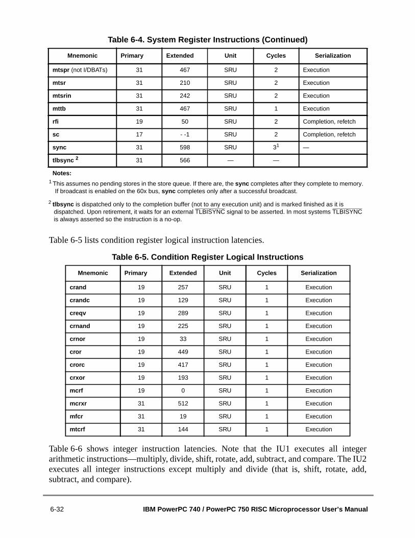
tegerIU2
add,
Table 6-5 lists condition register logical instruction latencies.
Table 6-6 shows integer instruction latencies. Note that the IU1 executes all inarithmetic instructions—multiply, divide, shift, rotate, add, subtract, and compare. Theexecutes all integer instructions except multiply and divide (that is, shift, rotate,subtract, and compare).
mtspr (not I/DBATs) 31 467 SRU 2 Execution
mtsr 31 210 SRU 2 Execution
mtsrin 31 242 SRU 2 Execution
mttb 31 467 SRU 1 Execution
rfi 19 50 SRU 2 Completion, refetch
sc 17 - -1 SRU 2 Completion, refetch
sync 31 598 SRU 31 —
tlbsync 2 31 566 — —
Notes:1 This assumes no pending stores in the store queue. If there are, the sync completes after they complete to memory.
If broadcast is enabled on the 60x bus, sync completes only after a successful broadcast.
2 tlbsync is dispatched only to the completion buffer (not to any execution unit) and is marked finished as it isdispatched. Upon retirement, it waits for an external TLBISYNC signal to be asserted. In most systems TLBISYNCis always asserted so the instruction is a no-op.
Table 6-5. Condition Register Logical Instructions
Mnemonic Primary Extended Unit Cycles Serialization
crand 19 257 SRU 1 Execution
crandc 19 129 SRU 1 Execution
creqv 19 289 SRU 1 Execution
crnand 19 225 SRU 1 Execution
crnor 19 33 SRU 1 Execution
cror 19 449 SRU 1 Execution
crorc 19 417 SRU 1 Execution
crxor 19 193 SRU 1 Execution
mcrf 19 0 SRU 1 Execution
mcrxr 31 512 SRU 1 Execution
mfcr 31 19 SRU 1 Execution
mtcrf 31 144 SRU 1 Execution
Table 6-4. System Register Instructions (Continued)
Mnemonic Primary Extended Unit Cycles Serialization
6-32 IBM PowerPC 740 / PowerPC 750 RISC Microprocessor User’s Manual

Table 6-6. Integer Instructions
Mnemonic Primary Extended Unit Cycles Serialization
addc [o][.] 31 10 IU1/IU2 1 —
adde [o][.] 31 138 IU1/IU2 1 Execution
addi 14 — IU1/IU2 1 —
addic 12 — IU1/IU2 1 —
addic. 13 — IU1/IU2 1 —
addis 15 — IU1/IU2 1 —
addme [o][.] 31 234 IU1/IU2 1 Execution
addze [o][.] 31 202 IU1/IU2 1 Execution
add [o][.] 31 266 IU1/IU2 1 —
andc [.] 31 60 IU1/IU2 1 —
andi. 28 — IU1/IU2 1 —
andis. 29 — IU1/IU2 1 —
and [.] 31 28 IU1/IU2 1 —
cmp 31 0 IU1/IU2 1 —
cmpi 11 — IU1/IU2 1 —
cmpl 31 32 IU1/IU2 1 —
cmpli 10 — IU1/IU2 1 —
cntlzw [.] 31 26 IU1/IU2 1 —
divwu [o][.] 31 459 IU1 19 —
divw [o][.] 31 491 IU1 19 —
eqv [.] 31 284 IU1/IU2 1 —
extsb [.] 31 954 IU1/IU2 1 —
extsh [.] 31 922 IU1/IU2 1 —
mulhwu [.] 31 11 IU1/IU2 2,3,4,5,6 —
mulhw [.] 31 75 IU1/IU2 2,3,4,5 —
mulli 7 — IU1 2,3 —
mull [o][.] 31 235 IU1 2,3,4,5 —
nand [.] 31 476 IU1/IU2 1 —
neg [o][.] 31 104 IU1/IU2 1 —
nor [.] 31 124 IU1/IU2 1 —
orc [.] 31 412 IU1/IU2 1 —
ori 24 — IU1/IU2 1 —
Chapter 6. Instruction Timing 6-33

ointashes.henon of
Table 6-7 shows latencies for floating-point instructions. Pipelined floating-pinstructions are shown with number of clocks in each pipeline stage separated by dFloating-point instructions with a single entry in the cycles column are not pipelined; wthe FPU executes these nonpipelined instructions, it remains busy for the full duratithe instruction execution and is not available for subsequent instructions.
oris 25 — IU1/IU2 1 —
or [.] 31 444 IU1/IU2 1 —
rlwimi [.] 20 — IU1/IU2 1 —
rlwinm [.] 21 — IU1/IU2 1 —
rlwnm [.] 23 — IU1/IU2 1 —
slw [.] 31 24 IU1/IU2 1 —
srawi [.] 31 824 IU1/IU2 1 —
sraw [.] 31 792 IU1/IU2 1 —
srw [.] 31 536 IU1/IU2 1 —
subfc [o][.] 31 8 IU1/IU2 1 —
subfe [o][.] 31 136 IU1/IU2 1 Execution
subfic 8 — IU1/IU2 1 —
subfme [o][.] 31 232 IU1/IU2 1 Execution
subfze [o][.] 31 200 IU1/IU2 1 Execution
subf [.] 31 40 IU1/IU2 1 —
tw 31 4 IU1/IU2 2 —
twi 3 — IU1/IU2 2 —
xori 26 — IU1/IU2 1 —
xoris 27 — IU1/IU2 1 —
xor [.] 31 316 IU1/IU2 1 —
Table 6-7. Floating-Point Instructions
Mnemonic Primary Extended Unit Cycles Serialization
fabs [.] 63 264 FPU 1-1-1 —
fadds [.] 59 21 FPU 1-1-1 —
fadd [.] 63 21 FPU 1-1-1 —
fcmpo 63 32 FPU 1-1-1 —
fcmpu 63 0 FPU 1-1-1 —
Table 6-6. Integer Instructions (Continued)
Mnemonic Primary Extended Unit Cycles Serialization
6-34 IBM PowerPC 740 / PowerPC 750 RISC Microprocessor User’s Manual

fctiwz [.] 63 15 FPU 1-1-1 —
fctiw [.] 63 14 FPU 1-1-1 —
fdivs [.] 59 18 FPU 17 —
fdiv [.] 63 18 FPU 31 —
fmadds [.] 59 29 FPU 1-1-1 —
fmadd [.] 63 29 FPU 2-1-1 —
fmr [.] 63 72 FPU 1-1-1 —
fmsubs [.] 59 28 FPU 1-1-1 —
fmsub [.] 63 28 FPU 2-1-1 —
fmuls [.] 59 25 FPU 1-1-1 —
fmul [.] 63 25 FPU 2-1-1 —
fnabs [.] 63 136 FPU 1-1-1 —
fneg [.] 63 40 FPU 1-1-1 —
fnmadds [.] 59 31 FPU 1-1-1 —
fnmadd [.] 63 31 FPU 2-1-1 —
fnmsubs [.] 59 30 FPU 1-1-1 —
fnmsub [.] 63 30 FPU 2-1-1 —
fres [.] 59 24 FPU 10 —
frsp [.] 63 12 FPU 1-1-1 —
frsqrte [.] 63 26 FPU 1-1-1 —
fsel [.] 63 23 FPU 1-1-1 —
fsubs [.] 59 20 FPU 1-1-1 —
fsub [.] 63 20 FPU 1-1-1 —
mcrfs 63 64 FPU 1-1-1 Execution
mffs [.] 63 583 FPU 1-1-1 Execution
mtfsb0 [.] 63 70 FPU 3 —
mtfsb1 [.] 63 38 FPU 3 —
mtfsfi [.] 63 134 FPU 3 —
mtfsf [.] 63 711 FPU 3 —
Table 6-7. Floating-Point Instructions (Continued)
Mnemonic Primary Extended Unit Cycles Serialization
Chapter 6. Instruction Timing 6-35

ns are
Table 6-8 shows load and store instruction latencies. Pipelined load/store instructioshown with cycles of total latency and throughput cycles separated by a colon.Table 6-8. Load and Store Instructions
Mnemonic Primary Extended Unit Cycles Serialization
dcbf 31 86 LSU 3:51 Execution
dcbi 31 470 LSU 3:31 Execution
dcbst 31 54 LSU 3:51 Execution
dcbt 31 278 LSU 2:1 —
dcbtst 31 246 LSU 2:1 —
dcbz 31 1014 LSU 3:61, 2 Execution
eciwx 31 310 LSU 2:1 —
ecowx 31 438 LSU 2:1 —
icbi 31 982 LSU 3:41 Execution
lbz 34 — LSU 2:1 —
lbzu 35 — LSU 2:1 —
lbzux 31 119 LSU 2:1 —
lbzx 31 87 LSU 2:1 —
lfd 50 — LSU 2:1 —
lfdu 51 — LSU 2:1 —
lfdux 31 631 LSU 2:1 —
lfdx 31 599 LSU 2:1 —
lfs 48 — LSU 2:1 —
lfsu 49 — LSU 2:1 —
lfsux 31 567 LSU 2:1 —
lfsx 31 535 LSU 2:1 —
lha 42 — LSU 2:1 —
lhau 43 — LSU 2:1 —
lhaux 31 375 LSU 2:1 —
lhax 31 343 LSU 2:1 —
lhbrx 31 790 LSU 2:1 —
lhz 40 — LSU 2:1 —
lhzu 41 — LSU 2:1 —
lhzux 31 311 LSU 2:1 —
lhzx 31 279 LSU 2:1 —
6-36 IBM PowerPC 740 / PowerPC 750 RISC Microprocessor User’s Manual

lmw 46 — LSU 2 + n 3 Completion, execution
lswi 31 597 LSU 2 + n 3 Completion, execution
lswx 31 533 LSU 2 + n 3 Completion, execution
lwarx 31 20 LSU 3:1 Execution
lwbrx 31 534 LSU 2:1 —
lwz 32 — LSU 2:1 —
lwzu 33 — LSU 2:1 —
lwzux 31 55 LSU 2:1 —
lwzx 31 23 LSU 2:1 —
stb 38 — LSU 2:1 —
stbu 39 — LSU 2:1 —
stbux 31 247 LSU 2:1 —
stbx 31 215 LSU 2:1 —
stfd 54 — LSU 2:1 —
stfdu 55 — LSU 2:1 —
stfdux 31 759 LSU 2:1 —
stfdx 31 727 LSU 2:1 —
stfiwx 31 983 LSU 2:1 —
stfs 52 — LSU 2:1 —
stfsu 53 — LSU 2:1 —
stfsux 31 695 LSU 2:1 —
stfsx 31 663 LSU 2:1 —
sth 44 — LSU 2:1 —
sthbrx 31 918 LSU 2:1 —
sthu 45 — LSU 2:1 —
sthux 31 439 LSU 2:1 —
sthx 31 407 LSU 2:1 —
stmw 47 — LSU 2 + n 3 Execution
stswi 31 725 LSU 2 + n 3 Execution
stswx 31 661 LSU 2 + n 3 Execution
stw 36 — LSU 2:1 —
stwbrx 31 662 LSU 2:1 —
Table 6-8. Load and Store Instructions (Continued)
Mnemonic Primary Extended Unit Cycles Serialization
Chapter 6. Instruction Timing 6-37

stwcx. 31 150 LSU 8:8 Execution
stwu 37 — LSU 2:1 —
stwux 31 183 LSU 2:1 —
stwx 31 151 LSU 2:1 —
tlbie 31 306 LSU 3:41 Execution
Notes :1 For cache-ops, the first number indicates the latency in finishing a single instruction; the second indicates the
throughput for back-to-back cache-ops. Throughput may be larger than the initial latency as more cycles may beneeded to complete the instruction to the cache, which stays busy keeping subsequent cache-ops from executing.
2 The throughput number of 6 cycles for dcbz assumes it is to nonglobal (M = 0) address space. For global addressspace, throughput is at least 11 cycles.
3 Load/store multiple/string instruction cycles are represented as a fixed number of cycles plus a variable number ofcycles, where n is the number of words accessed by the instruction.
Table 6-8. Load and Store Instructions (Continued)
Mnemonic Primary Extended Unit Cycles Serialization
6-38 IBM PowerPC 740 / PowerPC 750 RISC Microprocessor User’s Manual

ains ad and
ignals.er.
er,, or
of thes that
ship.
used
atas alsoignals
Chapter 7Signal Descriptions7070
This chapter describes the PowerPC 750 microprocessor’s external signals. It contconcise description of individual signals, showing behavior when the signal is assertenegated and when the signal is an input and an output.
NOTEA bar over a signal name indicates that the signal is activelow—for example,ARTRY (address retry) andTS (transferstart). Active-low signals are referred to as asserted (active)when they are low and negated when they are high. Signals thatare not active low, such as AP[0–3] (address bus parity signals)and TT[0–4] (transfer type signals) are referred to as assertedwhen they are high and negated when they are low.
The 750 signals are grouped as follows:
• Address arbitration—The 750 uses these signals to arbitrate for address busmastership.
• Address transfer start—These signals indicate that a bus master has begun atransaction on the address bus.
• Address transfer—These signals include the address bus and address parity sThey are used to transfer the address and to ensure the integrity of the transf
• Transfer attribute—These signals provide information about the type of transfsuch as the transfer size and whether the transaction is bursted, write-throughcache-inhibited.
• Address transfer termination—These signals are used to acknowledge the endaddress phase of the transaction. They also indicate whether a condition existrequires the address phase to be repeated.
• Data arbitration—The 750 uses these signals to arbitrate for data bus master
• Data transfer—These signals, which consist of the data bus and data parity, areto transfer the data and to ensure the integrity of the transfer.
• Data transfer termination—Data termination signals are required after each dbeat in a data transfer. In a single-beat transaction, the data termination signalindicate the end of the tenure; while in burst accesses, the data termination s
Chapter 7. Signal Descriptions 7-1

datato be
cessing
op and,
inity.
also
chipoard-
apply to individual beats and indicate the end of the tenure only after the finalbeat. They also indicate whether a condition exists that requires the data phaserepeated.
• L2 cache address/data—The 750 has separate address and data buses for acthe L2 cache (not supported in the PowerPC 740).
• L2 cache clock/control—These signals provide clocking and control for the L2cache (not supported in the 740).
• Interrupts/resets—These signals include the external interrupt signal, checkstsignals, and both soft reset and hard reset signals. They are used to interruptunder various conditions, to reset the processor.
• Processor status and control—These signals are used to set the reservationcoherency bit, enable the time base, and other functions. They are also used conjunction with such resources as secondary caches and the time base facil
• Clock control—These signals determine the system clock frequency. They canbe used to synchronize multiprocessor systems.
• Test interface—The JTAG (IEEE 1149.1a-1993) interface and the common on-processor (COP) unit provide a serial interface to the system for performing blevel boundary-scan interconnect tests.
7-2 IBM PowerPC 740 / PowerPC 750 RISC Microprocessor User’s Manual

ped.
7.1 Signal ConfigurationFigure 7-1 illustrates the 750’s signal configuration, showing how the signals are grouA pinout showing pin numbers is included in the 750 hardware specifications.
Figure 7-1. PowerPC 750 Signal Groups
DataArbitration
L2 CacheAddress/
Data
BRBG
ABB
TS
AP[0–3]
GBL
TSIZ[0–2]
AACK
ARTRY
SYSCLK
DBG
DBWO
DBB
D[0–63]
DP[0–7]
TADRTRY
TEA
INT
JTAG/COP
Factory Test
1
1
1
1
1
5
3
4
TBST
WT
PLL_CFG[0–3]
TT[0–4]5
4
TBEN
1CLK_OUT
MCP
SRESET
TLBISYNC
L2ADDR[16–0]
SMI
HRESET
QREQ
QACK
CKSTP_IN
CKSTP_OUT
L2DATA[0–63]
L2DP[0–7]
L2CEL2WEL2CLK_OUT[A–B]
1
3
1
1
1
1
1
1
1
8
64
1
1
1
1
1
1
1
1
1
1
1
1
1
1
1
CI 1
A[0–31]32
L2SYNC_OUT
AddressArbitration
AddressBus
L2SYNC_IN
L2ZZ
L2 CacheClock/
Control
AddressTermination
AddressStart
TransferAttributes
DataTransfer
DataTermination
Interrupts/Resets
ProcessorStatus/Control
VDD VDD (I/O)
ClockControl
TestInterface
RSRV
17
2
1
1
1
64
8
1
1
Not supported in the 740L2VDD
L2AVDD
750
DBDIS1
AVDD
Chapter 7. Signal Descriptions 7-3

thation,”ignals
est thes whent, see
e,uest
us.the
tionses
ted,
the
curs
7.2 Signal DescriptionsThis section describes individual 750 signals, grouped according to Figure 7-1. Notethe following sections summarize signal functions. Chapter 8, “Bus Interface Operatdescribes many of these signals in greater detail, both with respect to how individual sfunction and how groups of signals interact.
7.2.1 Address Bus Arbitration SignalsThe address arbitration signals are input and output signals the 750 uses to requaddress bus, recognize when the request is granted, and indicate to other devicemastership is granted. For a detailed description of how these signals interacSection 8.3.1, “Address Bus Arbitration.”
7.2.1.1 Bus Request ( BR)—OutputFollowing are the state meaning and timing comments for theBR output signal.
State Meaning Asserted—Indicates that the 750 is requesting mastership of thaddress bus. Note thatBR may be asserted for one or more cyclesand then de-asserted due to an internal cancellation of the bus req(for example, due to a load hit in the touch load buffer). SeeSection 8.3.1, “Address Bus Arbitration.”
Negated—Indicates that the 750 is not requesting the address bThe 750 may have no bus operation pending, it may be parked, orARTRY input was asserted on the previous bus clock cycle.
Timing Comments Assertion—Occurs when the 750 is not parked and a bus transacis needed. This may occur even if the two possible pipeline acceshave occurred.BR will also be asserted for one cycle during theexecution of adcbz instruction, and during the execution of a loadinstruction which hits in the touch load buffer.
Negation—Occurs for at least one bus clock cycle after an accepqualified bus grant (seeBG andABB), even if another transaction ispending. It is also negated for at least one bus clock cycle whenassertion ofARTRY is detected on the bus.
7.2.1.2 Bus Grant ( BG)—InputFollowing are the state meaning and timing comments for theBG input signal.
State Meaning Asserted—Indicates that the 750 may, with proper qualification,assume mastership of the address bus. A qualified bus grant ocwhenBG is asserted andABB andARTRY are not asserted the buscycle following the assertion ofAACK. TheABB andARTRYsignals are driven by the 750 or other bus masters. If the 750 isparked,BR need not be asserted for the qualified bus grant. SeeSection 8.3.1, “Address Bus Arbitration.”
7-4 IBM PowerPC 740 / PowerPC 750 RISC Microprocessor User’s Manual

bus
eheck
ion to
theycle
e
nt,
np,
r bus a
Negated— Indicates that the 750 is not the next potential addressmaster.
Timing Comments Assertion—May occur at any time to indicate the 750 can use thaddress bus. After the 750 assumes bus mastership, it does not cfor a qualified bus grant again until the cycle during which theaddress bus tenure completes (assuming it has another transactrun). The 750 does not accept aBG in the cycles between theassertion of anyTS andAACK.
Negation—May occur at any time to indicate the 750 cannot usebus. The 750 may still assume bus mastership on the bus clock cof the negation ofBG because during the previous cycleBGindicated to the 750 that it could take mastership (if qualified).
7.2.1.3 Address Bus Busy ( ABB)The address bus busy (ABB) signal is both an input and an output signal.
7.2.1.3.1 Address Bus Busy ( ABB)—OutputFollowing are the state meaning and timing comments for theABB output signal.
State Meaning Asserted—Indicates that the 750 is the address bus master. SeSection 8.3.1, “Address Bus Arbitration.”
Negated—Indicates that the 750 is not using the address bus. IfABBis negated during the bus clock cycle following a qualified bus grathe 750 did not accept mastership even ifBR was asserted. This canoccur if a potential transaction is aborted internally before thetransaction begins.
Timing Comments Assertion—Occurs on the bus clock cycle following a qualifiedBGthat is accepted by the processor (see Negated).
Negation—Occurs for a minimum of one-half bus clock cyclefollowing the assertion ofAACK. If ABB is negated during the busclock cycle after a qualified bus grant, the 750 did not acceptmastership, even ifBR was asserted.
High Impedance—Occurs afterABB is negated.
7.2.1.3.2 Address Bus Busy ( ABB)—InputFollowing are the state meaning and timing comments for theABB input signal.
State Meaning Asserted—Indicates that the address bus is in use. This conditioeffectively blocks the 750 from assuming address bus ownershiregardless of theBG input; see Section 8.3.1, “Address BusArbitration.”
Negated—Indicates that the address bus is not owned by anothemaster and that it is available to the 750 when accompanied byqualified bus grant.
Chapter 7. Signal Descriptions 7-5

e
us.
ss busry
.2,
s arelsoan
ction for
monitor, refer
Timing Comments Assertion—May occur when the 750 must be kept from using thaddress bus (and the processor is not currently assertingABB).
Negation—May occur whenever the 750 can use the address b
7.2.2 Address Transfer Start SignalsAddress transfer start signals are input and output signals that indicate that an addretransfer has begun. The transfer start (TS) signal identifies the operation as a memotransaction.
For detailed information about howTS interacts with other signals, refer to Section 8.3“Address Transfer.”
7.2.2.1 Transfer Start ( TS)TheTS signal is both an input and an output signal on the 750.
7.2.2.1.1 Transfer Start ( TS)—OutputFollowing are the state meaning and timing comments for theTS output signal.
State Meaning Asserted—Indicates that the 750 has begun a memory bustransaction and that the address bus and transfer attribute signalvalid. When asserted with the appropriate TT[0–4] signals it is aan implied data bus request for a memory transaction (unless it isaddress-only operation).
Negated—Indicates that no bus transaction is occurring duringnormal operation.
Timing Comments Assertion—Coincides with the assertion ofABB.Negation—Occurs one bus clock cycle afterTS is asserted.High Impedance—Coincides with the negation ofABB.
7.2.2.1.2 Transfer Start ( TS)—InputFollowing are the state meaning and timing comments for theTS input signal.
State Meaning Asserted—Indicates that another master has begun a bus transaand that the address bus and transfer attribute signals are validsnooping (seeGBL).
Negated—Indicates that no bus transaction is occurring.
Timing Comments Assertion—May occur during the assertion ofABB.Negation—Must occur one bus clock cycle afterTS is asserted.
7.2.3 Address Transfer SignalsThe address transfer signals are used to transmit the address and to generate andparity for the address transfer. For a detailed description of how these signals interactto Section 8.3.2, “Address Transfer.”
7-6 IBM PowerPC 740 / PowerPC 750 RISC Microprocessor User’s Manual

als.
s.
ss inurstdressd
not
ed
p
the
g onee bus.
ls on
s ofoddal
”
7.2.3.1 Address Bus (A[0–31])The address bus (A[0–31]) consists of 32 signals that are both input and output sign
7.2.3.1.1 Address Bus (A[0–31])—OutputFollowing are the state meaning and timing comments for the A[0–31] output signal
State Meaning Asserted/Negated—Represents the physical address (real addrethe architecture specification) of the data to be transferred. On btransfers, the address bus presents the double-word-aligned adcontaining the critical code/data that missed the cache on a reaoperation, or the first double word of the cache line on a writeoperation. Note that the address output during burst operations isincremented. See Section 8.3.2, “Address Transfer.”
Timing Comments Assertion/Negation—Occurs on the bus clock cycle after a qualifibus grant (coincides with assertion ofABB andTS).
High Impedance—Occurs one bus clock cycle afterAACK isasserted.
7.2.3.1.2 Address Bus (A[0–31])—InputFollowing are the state meaning and timing comments for the A[0–31] input signals.
State Meaning Asserted/Negated—Represents the physical address of a snoooperation.
Timing Comments Assertion/Negation—Must occur on the same bus clock cycle asassertion ofTS; is sampled by 750 only on this cycle.
7.2.3.2 Address Bus Parity (AP[0–3])The address bus parity (AP[0–3]) signals are both input and output signals reflectinbit of odd-byte parity for each of the 4 bytes of address when a valid address is on th
7.2.3.2.1 Address Bus Parity (AP[0–3])—OutputFollowing are the state meaning and timing comments for the AP[0–3] output signathe 750.
State Meaning Asserted/Negated—Represents odd parity for each of the 4 bytethe physical address for a transaction. Odd parity means that annumber of bits, including the parity bit, are driven high. The signassignments correspond to the following:
AP0 A[0–7]AP1 A[8–15]AP2 A[16–23]AP3 A[24–31]
For more information, see Section 8.3.2.1, “Address Bus Parity.
Timing Comments Assertion/Negation—The same as A[0–31].High Impedance—The same as A[0–31].
Chapter 7. Signal Descriptions 7-7

n the
s ofrityr the0ent
suchburst, see
mory
or a-1.
ls on
n the
ee
7.2.3.2.2 Address Bus Parity (AP[0–3])—InputFollowing are the state meaning and timing comments for the AP[0–3] input signal o750.
State Meaning Asserted/Negated—Represents odd parity for each of the 4 bytethe physical address for snooping operations. Detected even pacauses the processor to take a machine check exception or entecheckstop state if address parity checking is enabled in the HIDregister; see Section 2.1.2.2, “Hardware Implementation-DependRegister 0.”
Timing Comments Assertion/Negation—The same as A[0–31].
7.2.4 Address Transfer Attribute SignalsThe transfer attribute signals are a set of signals that further characterize the transfer—as the size of the transfer, whether it is a read or write operation, and whether it is aor single-beat transfer. For a detailed description of how these signals interactSection 8.3.2, “Address Transfer.”
Note that some signal functions vary depending on whether the transaction is a meaccess or an I/O access.
7.2.4.1 Transfer Type (TT[0–4])The transfer type (TT[0–4]) signals consist of five input/output signals on the 750. Fcomplete description of TT[0–4] signals and for transfer type encodings, see Table 7
7.2.4.1.1 Transfer Type (TT[0–4])—OutputFollowing are the state meaning and timing comments for the TT[0–4] output signathe 750.
State Meaning Asserted/Negated—Indicates the type of transfer in progress.
Timing Comments Assertion/Negation/High Impedance—The same as A[0–31].
7.2.4.1.2 Transfer Type (TT[0–4])—InputFollowing are the state meaning and timing comments for the TT[0–4] input signals o750.
State Meaning Asserted/Negated—Indicates the type of transfer in progress (sTable 7-2).
Timing Comments Assertion/Negation—The same as A[0–31].
7-8 IBM PowerPC 740 / PowerPC 750 RISC Microprocessor User’s Manual

Table 7-1 describes the transfer encodings for an 750 bus master.
Table 7-1. Transfer Type Encodings for PowerPC 750 Bus Master
PowerPC 750Bus MasterTransaction
TransactionSource
TT0 TT1 TT2 TT3 TT460x Bus
SpecificationCommand
Transaction
Address only1 dcbst 0 0 0 0 0 Clean block Address only
Address only1 dcbf 0 0 1 0 0 Flush block Address only
Address only1 sync 0 1 0 0 0 sync Address only
Address only1 dcbz or dcbi 0 1 1 0 0 Kill block Address only
Address only1 eieio 1 0 0 0 0 eieio Address only
Single-beatwrite (nonGBL)
ecowx 1 0 1 0 0 External controlword write
Single-beatwrite
N/A N/A 1 1 0 0 0 TLB invalidate Address only
Single-beatread (nonGBL)
eciwx 1 1 1 0 0 External controlword read
Single-beatread
N/A N/A 0 0 0 0 1 lwarxreservation set
Address only
N/A N/A 0 0 1 0 1 Reserved —
N/A N/A 0 1 0 0 1 tlbsync Address only
N/A N/A 0 1 1 0 1 icbi Address only
N/A N/A 1 X X 0 1 Reserved —
Single-beatwrite
Caching-inhibitedor write-throughstore
0 0 0 1 0 Write-with-flush Single-beatwrite or burst
Burst(nonGBL)
Cast-out, orsnoop copyback
0 0 1 1 0 Write-with-kill Burst
Single-beatread
Caching-inhibitedload or instructionfetch
0 1 0 1 0 Read Single-beatread or burst
Burst Load miss, storemiss, orinstruction fetch
0 1 1 1 0 Read-with-intent-to-modify
Burst
Single-beatwrite
stwcx. 1 0 0 1 0 Write-with-flush-atomic
Single-beatwrite
N/A N/A 1 0 1 1 0 Reserved N/A
Single-beatread
lwarx (caching-inhibited load)
1 1 0 1 0 Read-atomic Single-beatread or burst
Burst lwarx(load miss)
1 1 1 1 0 Read-with-intent-to-modify-atomic
Burst
N/A N/A 0 0 0 1 1 Reserved —
Chapter 7. Signal Descriptions 7-9

snoop
Table 7-2 describes the 60x bus specification transfer encodings and the 750 busresponse on an address hit.N/A N/A 0 0 1 1 1 Reserved —
N/A N/A 0 1 0 1 1 Read-with-no-intent-to-cache
Single-beatread or burst
N/A N/A 0 1 1 1 1 Reserved —
N/A N/A 1 X X 1 1 Reserved —
Note : 1Address-only transaction occurs if enabled by setting HID0[ABE] bit to 1.
Table 7-2. PowerPC 750 Snoop Hit Response
60x Bus SpecificationCommand
Transaction TT0 TT1 TT2 TT3 TT4PowerPC 750Bus Snooper;Action on Hit
Clean block Address only 0 0 0 0 0 N/A
Flush block Address only 0 0 1 0 0 N/A
sync Address only 0 1 0 0 0 N/A
Kill block Address only 0 1 1 0 0 Flush, cancelreservation
eieio Address only 1 0 0 0 0 N/A
External control word write Single-beat write 1 0 1 0 0 N/A
TLB Invalidate Address only 1 1 0 0 0 N/A
External control word read Single-beat read 1 1 1 0 0 N/A
lwarxreservation set
Address only 0 0 0 0 1 N/A
Reserved — 0 0 1 0 1 N/A
tlbsync Address only 0 1 0 0 1 N/A
icbi Address only 0 1 1 0 1 N/A
Reserved — 1 X X 0 1 N/A
Write-with-flush Single-beat write or burst 0 0 0 1 0 Flush, cancelreservation
Write-with-kill Single-beat write or burst 0 0 1 1 0 Kill, cancelreservation
Read Single-beat read or burst 0 1 0 1 0 Clean or flush
Read-with-intent-to-modify Burst 0 1 1 1 0 Flush
Table 7-1. Transfer Type Encodings for PowerPC 750 Bus Master (Continued)
PowerPC 750Bus MasterTransaction
TransactionSource
TT0 TT1 TT2 TT3 TT460x Bus
SpecificationCommand
Transaction
7-10 IBM PowerPC 740 / PowerPC 750 RISC Microprocessor User’s Manual

–2])
with, asareowsforible
7.2.4.2 Transfer Size (TSIZ[0–2])—OutputFollowing are the state meaning and timing comments for the transfer size (TSIZ[0output signals on the 750.
State Meaning Asserted/Negated—For memory accesses, these signals alongTBST, indicate the data transfer size for the current bus operationshown in Table 7-3. Table 8-4 shows how the transfer size signalsused with the address signals for aligned transfers. Table 8-5 shhow the transfer size signals are used with the address signals misaligned transfers. Note that the 750 does not generate all possTSIZ[0–2] encodings.
For external control instructions (eciwxandecowx), TSIZ[0–2] areused to output bits 29–31 of the external access register (EAR),which are used to form the resource ID (TBST||TSIZ0–TSIZ2).
Timing Comments Assertion/Negation—The same as A[0–31].High Impedance—The same as A[0–31].
Write-with-flush-atomic Single-beat write 1 0 0 1 0 Flush, cancelreservation
Reserved N/A 1 0 1 1 0 N/A
Read-atomic Single-beat read or burst 1 1 0 1 0 Clean or flush
Read-with-intent-to modify-atomic
Burst 1 1 1 1 0 Flush
Reserved — 0 0 0 1 1 N/A
Reserved — 0 0 1 1 1 N/A
Read-with-no-intent-to-cache Single-beat read or burst 0 1 0 1 1 Clean
Reserved — 0 1 1 1 1 N/A
Reserved — 1 X X 1 1 N/A
Table 7-3. Data Transfer Size
TBST TSIZ[0–2] Transfer Size
Asserted 010 Burst (32 bytes)
Negated 000 8 bytes
Negated 001 1 byte
Negated 010 2 bytes
Negated 011 3 bytes
Table 7-2. PowerPC 750 Snoop Hit Response (Continued)
60x Bus SpecificationCommand
Transaction TT0 TT1 TT2 TT3 TT4PowerPC 750Bus Snooper;Action on Hit
Chapter 7. Signal Descriptions 7-11
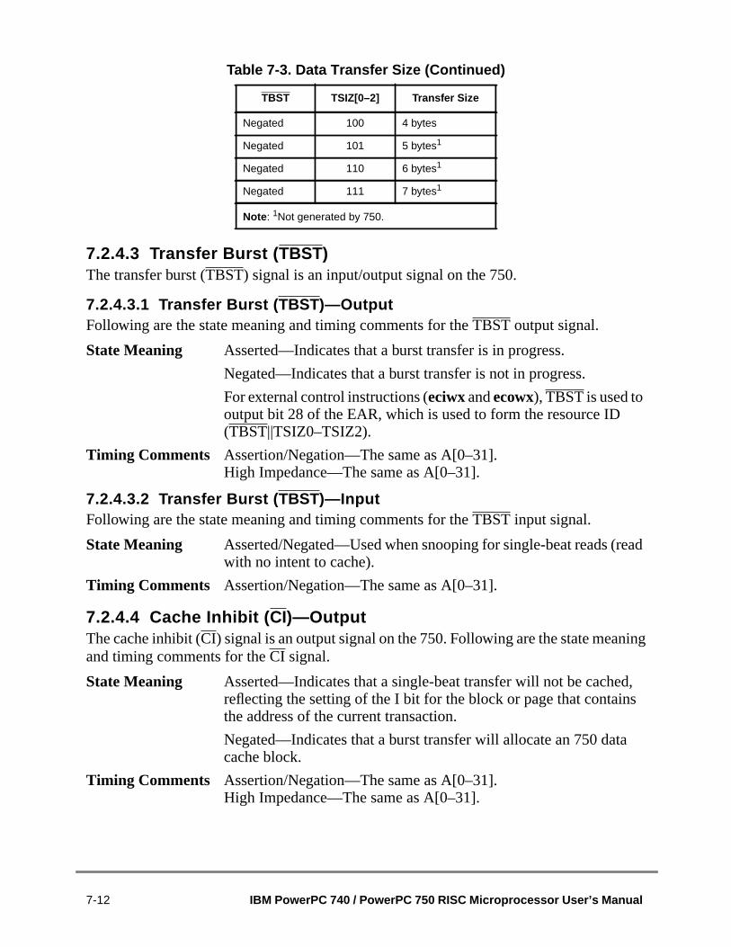
read
ning
d,ns
a
7.2.4.3 Transfer Burst ( TBST)The transfer burst (TBST) signal is an input/output signal on the 750.
7.2.4.3.1 Transfer Burst ( TBST)—OutputFollowing are the state meaning and timing comments for theTBST output signal.
State Meaning Asserted—Indicates that a burst transfer is in progress.
Negated—Indicates that a burst transfer is not in progress.
For external control instructions (eciwxandecowx), TBST is used tooutput bit 28 of the EAR, which is used to form the resource ID(TBST||TSIZ0–TSIZ2).
Timing Comments Assertion/Negation—The same as A[0–31].High Impedance—The same as A[0–31].
7.2.4.3.2 Transfer Burst ( TBST)—InputFollowing are the state meaning and timing comments for theTBST input signal.
State Meaning Asserted/Negated—Used when snooping for single-beat reads (with no intent to cache).
Timing Comments Assertion/Negation—The same as A[0–31].
7.2.4.4 Cache Inhibit ( CI)—OutputThe cache inhibit (CI) signal is an output signal on the 750. Following are the state meaand timing comments for theCI signal.
State Meaning Asserted—Indicates that a single-beat transfer will not be cachereflecting the setting of the I bit for the block or page that contaithe address of the current transaction.
Negated—Indicates that a burst transfer will allocate an 750 datcache block.
Timing Comments Assertion/Negation—The same as A[0–31].High Impedance—The same as A[0–31].
Negated 100 4 bytes
Negated 101 5 bytes1
Negated 110 6 bytes1
Negated 111 7 bytes1
Note : 1Not generated by 750.
Table 7-3. Data Transfer Size (Continued)
TBST TSIZ[0–2] Transfer Size
7-12 IBM PowerPC 740 / PowerPC 750 RISC Microprocessor User’s Manual

ate
-at a
;
tingeand
750.
0.
phaseuld be8.3.3,
7.2.4.5 Write-Through ( WT)—OutputThe write-through (WT) signal is an output signal on the 750. Following are the stmeaning and timing comments for theWT signal.
State Meaning Asserted—Indicates that a single-beat write transaction is writethrough, reflecting the value of the W bit for the block or page thcontains the address of the current transaction. Assertion duringread operation indicates instruction fetching.
Negated—Indicates that a write transaction is not write-throughduring a read operation negation indicates a data load.
Timing Comments Assertion/Negation—The same as A[0–31].High Impedance—The same as A[0–31].
7.2.4.6 Global ( GBL)The global (GBL) signal is an input/output signal on the 750.
7.2.4.6.1 Global ( GBL)—OutputFollowing are the state meaning and timing comments for theGBL output signal.
State Meaning Asserted—Indicates that a transaction is global, reflecting the setof the M bit for the block or page that contains the address of thcurrent transaction (except in the case of copy-back operations instruction fetches, which are nonglobal.)
Negated—Indicates that a transaction is not global.
Timing Comments Assertion/Negation—The same as A[0–31].High Impedance—The same as A[0–31].
7.2.4.6.2 Global ( GBL)—InputFollowing are the state meaning and timing comments for theGBL input signal.
State Meaning Asserted—Indicates that a transaction must be snooped by the
Negated—Indicates that a transaction is not snooped by the 75
Timing Comments Assertion/Negation—The same as A[0–31].
7.2.5 Address Transfer Termination SignalsThe address transfer termination signals are used to indicate either that the addressof the transaction has completed successfully or must be repeated, and when it shoterminated. For detailed information about how these signals interact, see Section“Address Transfer Termination.”
Chapter 7. Signal Descriptions 7-13

re
the
ccesstsrtion
f
dateserts
ped
of
es,nceckto
7.2.5.1 Address Acknowledge ( AACK)—InputThe address acknowledge (AACK) signal is an input-only signal on the 750. Following athe state meaning and timing comments for theAACK signal.
State Meaning Asserted—Indicates that the address phase of a transaction iscomplete. The address bus will go to a high-impedance state onnext bus clock cycle. The 750 samplesARTRY on the bus clockcycle following the assertion ofAACK.
Negated—(DuringABB) indicates that the address bus and thetransfer attributes must remain driven.
Timing Comments Assertion—May occur as early as the bus clock cycle afterTS isasserted; assertion can be delayed to allow adequate address atime for slow devices. For example, if an implementation supporslow snooping devices, an external arbiter can postpone the asseof AACK.
Negation—Must occur one bus clock cycle after the assertion oAACK.
7.2.5.2 Address Retry ( ARTRY)The address retry (ARTRY) signal is both an input and output signal on the 750.
7.2.5.2.1 Address Retry ( ARTRY)—OutputFollowing are the state meaning and timing comments for theARTRY output signal.
State Meaning Asserted—Indicates that the 750 detects a condition in which asnooped address tenure must be retried. If the 750 needs to upmemory as a result of the snoop that caused the retry, the 750 asBR the second cycle afterAACK if ARTRY is asserted.
High Impedance—Indicates that the 750 does not need the snooaddress tenure to be retried.
Timing Comments Assertion—Asserted the third bus cycle following the assertion TS if a retry is required.
Negation—Occurs the second bus cycle after the assertion ofAACK.Since this signal may be simultaneously driven by multiple devicit negates in a unique fashion. First the buffer goes to high impedafor a minimum of one-half processor cycle (dependent on the clomode), then it is driven negated for one bus cycle before returninghigh impedance.
This special method of negation may be disabled by settingprecharge disable in HID0.
7-14 IBM PowerPC 740 / PowerPC 750 RISC Microprocessor User’s Manual

telyyf thester,
te
d to
ely
f
rderlysignal
orhow
ut
ate
n, data
7.2.5.2.2 Address Retry ( ARTRY)—InputFollowing are the state meaning and timing comments for theARTRY input signal.
State Meaning Asserted—If the 750 is the address bus master,ARTRY indicatesthat the 750 must retry the preceding address tenure and immedianegateBR (if asserted). If the associated data tenure has alreadstarted, the 750 also aborts the data tenure immediately, even iburst data has been received. If the 750 is not the address bus mathis input indicates that the 750 should immediately negateBR toallow an opportunity for a copy-back operation to main memoryafter a snooping bus master assertsARTRY. Note that the subsequenaddress presented on the address bus may not be the same onassociated with the assertion of theARTRY signal.
Negated/High Impedance—Indicates that the 750 does not neeretry the last address tenure.
Timing Comments Assertion—May occur as early as the second cycle following thassertion ofTS, and must occur by the bus clock cycle immediatefollowing the assertion ofAACK if an address retry is required.
Negation—Must occur two bus clock cycles after the assertion oAACK.
7.2.6 Data Bus Arbitration SignalsLike the address bus arbitration signals, data bus arbitration signals maintain an oprocess for determining data bus mastership. Note that there is no data bus arbitrationequivalent to the address bus arbitration signalBR (bus request), because, except faddress-only transactions,TS implies data bus requests. For a detailed description onthese signals interact, see Section 8.4.1, “Data Bus Arbitration.”
One special signal,DBWO, allows the 750 to be configured dynamically to write data oof order with respect to read data. For detailed information about usingDBWO, seeSection 8.10, “Using Data Bus Write Only.”
7.2.6.1 Data Bus Grant ( DBG)—InputThe data bus grant (DBG) signal is an input-only signal on the 750. Following are the stmeaning and timing comments for theDBG signal.
State Meaning Asserted—Indicates that the 750 may, with the proper qualificatioassume mastership of the data bus. The 750 derives a qualifiedbus grant whenDBG is asserted andDBB, DRTRY, andARTRY arenegated; that is, the data bus is not busy (DBB is negated), there is nooutstanding attempt to retry the current data tenure (DRTRY isnegated), and there is no outstanding attempt to perform anARTRYof the associated address tenure.
Negated—Indicates that the 750 must hold off its data tenures.
Chapter 7. Signal Descriptions 7-15

e
me
re
r anfore
the
ing
0d is
d
Timing Comments Assertion—May occur any time to indicate the 750 is free to takdata bus mastership. It is not sampled untilTS is asserted.
Negation—May occur at any time to indicate the 750 cannot assudata bus mastership.
7.2.6.2 Data Bus Write Only ( DBWO)—InputThe data bus write only (DBWO) signal is an input-only signal on the 750. Following athe state meaning and timing comments for theDBWO signal.
State Meaning Asserted—Indicates that the 750 may run the data bus tenure fooutstanding write address even if a read address is pipelined bethe write address. Refer to Section 8.10, “Using Data Bus WriteOnly,” for detailed instructions for usingDBWO.
Negated—Indicates that the 750 must run the data bus tenures insame order as the address tenures.
Timing Comments Assertion—Must occur no later than a qualifiedDBG for anoutstanding write tenure.DBWO is sampled by the 750 on the clockof a qualifiedDBG. If no write requests are pending, the 750 willignoreDBWO and assume data bus ownership for the next pendread request.
Negation—May occur any time after a qualifiedDBG and before thenext assertion ofDBG.
7.2.6.3 Data Bus Busy ( DBB)The data bus busy (DBB) signal is both an input and output signal on the 750.
7.2.6.3.1 Data Bus Busy ( DBB)—OutputFollowing are the state meaning and timing comments for theDBB output signal.
State Meaning Asserted—Indicates that the 750 is the data bus master. The 75always assumes data bus mastership if it needs the data bus angiven a qualified data bus grant (seeDBG).
Negated—Indicates that the 750 is not using the data bus.
Timing Comments Assertion—Occurs during the bus clock cycle following a qualifieDBG.
Negation—Occurs for a minimum of one-half bus clock cycle(dependent on clock mode) following the assertion of the finalTA.
High Impedance—Occurs afterDBB is negated.
7.2.6.3.2 Data Bus Busy ( DBB)—InputFollowing are the state meaning and timing comments for theDBB input signal.
State Meaning Asserted—Indicates that another device is bus master.Negated—Indicates that the data bus is free (with properqualification, seeDBG) for use by the 750.
7-16 IBM PowerPC 740 / PowerPC 750 RISC Microprocessor User’s Manual

ing
and todata
andand
low
r
nals.
te.ta.
of
Timing Comments Assertion—Must occur when the 750 must be prevented from usthe data bus.
Negation—May occur whenever the data bus is available.
7.2.7 Data Transfer SignalsLike the address transfer signals, the data transfer signals are used to transmit datagenerate and monitor parity for the data transfer. For a detailed description of how thetransfer signals interact, see Section 8.4.3, “Data Transfer.”
7.2.7.1 Data Bus (DH[0–31], DL[0–31])The data bus (DH[0–3]1 and DL[0–31]) consists of 64 signals that are both inputsoutputs on the 750. Following are the state meaning and timing comments for the DHDL signals.
State Meaning The data bus has two halves—data bus high (DH) and data bus(DL). See Table 7-4 for the data bus lane assignments.
Timing Comments The data bus is driven once for noncached transactions and foutimes for cache transactions (bursts).
7.2.7.1.1 Data Bus (DH[0–31], DL[0–31])—OutputFollowing are the state meaning and timing comments for the DH and DL output sig
State Meaning Asserted/Negated—Represents the state of data during a data wriByte lanes not selected for data transfer will not supply valid da
Timing Comments Assertion/Negation—Initial beat coincides withDBB and, forbursts, transitions on the bus clock cycle following each assertionTA.
High Impedance—Occurs on the bus clock cycle after the finalassertion ofTA, following the assertion ofTEA, or in certainARTRY cases.
Table 7-4. Data Bus Lane Assignments
Data Bus Signals Byte Lane
DH[0–7] 0
DH[8–15] 1
DH[16–23] 2
DH[24–31] 3
DL[0–7] 4
DL[8–15] 5
DL[16–23] 6
DL[24–31] 7
Chapter 7. Signal Descriptions 7-17

als.
read
cle
nals.
s ofits,
is
ata.therors
7.2.7.1.2 Data Bus (DH[0–31], DL[0–31])—InputFollowing are the state meaning and timing comments for the DH and DL input sign
State Meaning Asserted/Negated—Represents the state of data during a data transaction.
Timing Comments Assertion/Negation—Data must be valid on the same bus clock cythatTA is asserted.
7.2.7.2 Data Bus Parity (DP[0–7])The eight data bus parity (DP[0–7]) signals on the 750 are both output and input sig
7.2.7.2.1 Data Bus Parity (DP[0–7])—OutputFollowing are the state meaning and timing comments for the DP output signals.
State Meaning Asserted/Negated—Represents odd parity for each of the 8 bytedata write transactions. Odd parity means that an odd number of bincluding the parity bit, are driven high. The generation of parityenabled through HID0. The signal assignments are listed inTable 7-5.
Timing Comments Assertion/Negation—The same as DL[0–31].High Impedance—The same as DL[0–31].
7.2.7.2.2 Data Bus Parity (DP[0–7])—InputFollowing are the state meaning and timing comments for the DP input signals.
State Meaning Asserted/Negated—Represents odd parity for each byte of read dParity is checked on all data byte lanes, regardless of the size oftransfer. Detected even parity causes a checkstop if data parity erare enabled in the HID0 register.
Timing Comments Assertion/Negation—The same as DL[0–31].
Table 7-5. DP[0–7] Signal Assignments
Signal Name Signal Assignments
DP0 DH[0–7]
DP1 DH[8–15]
DP2 DH[16–23]
DP3 DH[24–31]
DP4 DL[0–7]
DP5 DL[8–15]
DP6 DL[16–23]
DP7 DL[24–31]
7-18 IBM PowerPC 740 / PowerPC 750 RISC Microprocessor User’s Manual
ring
the
.
theed
at in aenure,dicate
ansfer
).
.”
t to
ataur at
o
y)rt
7.2.7.3 Data Bus Disable ( DBDIS)—InputFollowing are the state meaning and timing comments for theDBDIS signal.
State Meaning Asserted—Indicates (for a write transaction) that the 750 mustrelease the data bus and the data bus parity to high impedance duthe following cycle. The data tenure remains active,DBB remainsdriven, and the transfer termination signals are still monitored by750.
Negated—Indicates the data bus should remain normally drivenDBDIS is ignored during read transactions.
Timing Comments Assertion/Negation—May be asserted on any clock cycle when750 is driving or will be driving the data bus; may remain assertmultiple cycles.
7.2.8 Data Transfer Termination SignalsData termination signals are required after each data beat in a data transfer. Note thsingle-beat transaction, the data termination signals also indicate the end of the twhile in burst accesses, the data termination signals apply to individual beats and inthe end of the tenure only after the final data beat.
For a detailed description of how these signals interact, see Section 8.4.4, “Data TrTermination.”
7.2.8.1 Transfer Acknowledge ( TA)—InputFollowing are the state meaning and timing comments for theTA signal.
State Meaning Asserted— Indicates that a single-beat data transfer completedsuccessfully or that a data beat in a burst transfer completedsuccessfully (unlessDRTRY is asserted on the next bus clock cycleNote thatTA must be asserted for each data beat in a bursttransaction and must be asserted during assertion ofDRTRY. Formore information, see Section 8.4.4, “Data Transfer Termination
Negated—(DuringDBB) indicates that, untilTA is asserted, the 750must continue to drive the data for the current write or must waisample the data for reads.
Timing Comments Assertion—Must not occur beforeAACK for the current transaction(if the address retry mechanism is to be used to prevent invalid dfrom being used by the processor); otherwise, assertion may occany time during the assertion ofDBB. The system can withholdassertion ofTA to indicate that the 750 should insert wait states textend the duration of the data beat.
Negation—Must occur after the bus clock cycle of the final (or onldata beat of the transfer. For a burst transfer, the system can asseTA
Chapter 7. Signal Descriptions 7-19

eat.
the
r
ta
e
nt
areas
for one bus clock cycle and then negate it to advance the bursttransfer to the next beat and insert wait states during the next b
7.2.8.2 Data Retry ( DRTRY)—InputFollowing are the state meaning and timing comments for theDRTRY signal.
State Meaning Asserted—Indicates that the 750 must invalidate the data from previous read operation.
Negated—Indicates that data presented withTA on the previous readoperation is valid. Note thatDRTRY is ignored for writetransactions.
Timing Comments Assertion—Must occur during the bus clock cycle immediately afteTA is asserted if a retry is required. TheDRTRY signal may be heldasserted for multiple bus clock cycles. WhenDRTRY is negated,data must have been valid on the previous clock withTA asserted.
Negation—Must occur during the bus clock cycle after a valid dabeat. This may occur several cycles afterDBB is negated, effectivelyextending the data bus tenure.
Start-up—TheDRTRY signal is sampled at the negation ofHRESET; ifDRTRY is asserted, no-DRTRY mode is selected. IfDRTRY is negated at start-up,DRTRY is enabled.
7.2.8.3 Transfer Error Acknowledge ( TEA)—InputFollowing are the state meaning and timing comments for theTEA signal.
State Meaning Asserted—Indicates that a bus error occurred. Causes a machincheck exception (and possibly causes the processor to entercheckstop state if machine check enable bit is cleared(MSR[ME] = 0)). For more information, see Section 4.5.2.2,“Checkstop State (MSR[ME] = 0).” Assertion terminates the curretransaction; that is, assertion ofTA andDRTRY are ignored. Theassertion ofTEA causes the negation/high impedance ofDBB in thenext clock cycle. However, data entering the GPR or the cache not invalidated. (Note that the term ‘exception’ is also referred to‘interrupt’ in the architecture specification.)
Negated—Indicates that no bus error was detected.
Timing Comments Assertion—May be asserted whileDBB is asserted, and the cycleafterTA during a read operation.TEA should be asserted for onecycle only.
Negation—TEA must be negated no later than the negation ofDBB.
7-20 IBM PowerPC 740 / PowerPC 750 RISC Microprocessor User’s Manual

eived,e 750r aReset
50
l
n if
lly
7.2.9 System Status SignalsMost system status signals are input signals that indicate when exceptions are recwhen checkstop conditions have occurred, and when the 750 must be reset. Thgenerates the output signal,CKSTP_OUT, when it detects a checkstop condition. Fodetailed description of these signals, see Section 8.7, “Interrupt, Checkstop, andSignals.”
7.2.9.1 Interrupt ( INT)—InputFollowing are the state meaning and timing comments for theINT signal.
State Meaning Asserted—The 750 initiates an interrupt if MSR[EE] is set;otherwise, the 750 ignores the interrupt. To guarantee that the 7will take the external interrupt,INT must be held active until the 750takes the interrupt; otherwise, whether the 750 takes an externainterrupt depends on whether the MSR[EE] bit was set while theINTsignal was held active.
Negated—Indicates that normal operation should proceed. SeeSection 8.7.1, “External Interrupts.”
Timing Comments Assertion—May occur at any time and may be assertedasynchronously to the input clocks. TheINT input is level-sensitive.Negation—Should not occur until interrupt is taken.
7.2.9.2 System Management Interrupt ( SMI)—InputFollowing are the state meaning and timing comments forSMI.
State Meaning Asserted—The 750 initiates a system management interruptoperation if the MSR[EE] is set; otherwise, the 750 ignores theexception condition. The system must holdSMI active until theexception is taken.
Negated—Indicates that normal operation should proceed. SeeSection 8.7.1, “External Interrupts.”
Timing Comments Assertion—May occur at any time and may be assertedasynchronously to the input clocks. TheSMI input is level-sensitive.
. Negation—Should not occur until interrupt is taken.
7.2.9.3 Machine Check Interrupt ( MCP)—InputFollowing are the state meaning and timing comments for theMCP signal.
State Meaning Asserted—The 750 initiates a machine check interrupt operatioMSR[ME] and HID0[EMCP] are set; if MSR[ME] is cleared andHID0[EMCP] is set, the 750 must terminate operation by internagating off all clocks, and releasing all outputs (exceptCKSTP_OUT)to the high-impedance state. If HID0[EMCP] is cleared, the 750
Chapter 7. Signal Descriptions 7-21

reset.
rnalethe
ition
ignores the interrupt condition. TheMCP signal must be heldasserted for two bus clock cycles.
Negated—Indicates that normal operation should proceed. SeeSection 8.7.1, “External Interrupts.”
Timing Comments Assertion—May occur at any time and may be assertedasynchronously to the input clocks. TheMCP input is negative edge-sensitive.
Negation—May be negated two bus cycles after assertion.
7.2.9.4 Checkstop Input ( CKSTP_IN)—InputFollowing are the state meaning and timing comments for theCKSTP_IN signal.
State Meaning Asserted—Indicates that the 750 must terminate operation byinternally gating off all clocks, and release all outputs (exceptCKSTP_OUT) to the high-impedance state. OnceCKSTP_IN hasbeen asserted it must remain asserted until the system has been
Negated—Indicates that normal operation should proceed. SeeSection 8.7.2, “Checkstops.”
Timing Comments Assertion—May occur at any time and may be assertedasynchronously to the input clocks.
Negation—May occur any time after theCKSTP_OUT output signalhas been asserted.
7.2.9.5 Checkstop Output ( CKSTP_OUT)—OutputNote that theCKSTP_OUT signal is an open-drain type output, and requires an extepull-up resistor (for example, 10 k to Vdd) to assure proper de-assertion of thCKSTP_OUT signal. Following are the state meaning and timing comments forCKSTP_OUT signal.
State Meaning Asserted—Indicates that the 750 has detected a checkstop condand has ceased operation.
Negated—Indicates that the 750 is operating normally.See Section 8.7.2, “Checkstops.”
Timing Comments Assertion—May occur at any time and may be assertedasynchronously to the 750 input clocks.
Negation—Is negated upon assertion ofHRESET.
7.2.9.6 Reset SignalsThere are two reset signals on the 750—hard reset (HRESET) and soft reset (SRESET).Descriptions of the reset signals are as follows:
7-22 IBM PowerPC 740 / PowerPC 750 RISC Microprocessor User’s Manual

iming
putas.”
r aet.
th
d in
emory, and
750
7.2.9.6.1 Hard Reset ( HRESET)—InputThe hard reset (HRESET) signal must be used at power-on in conjunction with theTRSTsignal to properly reset the processor. Following are the state meaning and tcomments for theHRESET signal.
State Meaning Asserted—Initiates a complete hard reset operation when this intransitions from asserted to negated. Causes a reset exception described in Section 4.5.1, “System Reset Exception (0x00100)Output drivers are released to high impedance within five clocksafter the assertion ofHRESET.
Negated—Indicates that normal operation should proceed. SeeSection 8.7.3, “Reset Inputs.”
Timing Comments Assertion—May occur at any time and may be assertedasynchronously to the 750 input clock; must be held asserted fominimum of 255 clock cycles after the PLL lock time has been mRefer to the 750 hardware specifications for further timingcomments.
Negation—May occur any time after the minimum reset pulse widhas been met.
This input has additional functionality in certain test modes.
7.2.9.6.2 Soft Reset ( SRESET)—InputFollowing are the state meaning and timing comments for theSRESET signal.
State Meaning Asserted— Initiates processing for a reset exception as describeSection 4.5.1, “System Reset Exception (0x00100).”
Negated—Indicates that normal operation should proceed. SeeSection 8.7.3, “Reset Inputs.”
Timing Comments Assertion—May occur at any time and may be assertedasynchronously to the 750 input clock. TheSRESET input isnegative edge-sensitive.
Negation—May be negated two bus cycles after assertion.
This input has additional functionality in certain test modes.
7.2.9.7 Processor Status SignalsProcessor status signals indicate the state of the processor. This includes the mreservation signal, machine quiesce control signals, time base enable signalTLBISYNC signal.
7.2.9.7.1 Quiescent Request ( QREQ)—OutputFollowing are the state meaning and timing comments forQREQ.
State Meaning Asserted—Indicates that the 750 is requesting all bus activitynormally required to be snooped to terminate or to pause so the
Chapter 7. Signal Descriptions 7-23

ed a
the
ast (or
, and
us
CK
the
.
may enter a quiescent (low power) state. When the 750 has enterquiescent state, it no longer snoops bus activity.
Negated—Indicates that the 750 is not making a request to enterquiescent state.
Timing Comments Assertion/Negation—May occur on any cycle.QREQ will remainasserted for the duration of the quiescent state.
7.2.9.7.2 Quiescent Acknowledge ( QACK)—InputFollowing are the state meaning and timing comments for theQACK signal.
State Meaning Asserted—Indicates that all bus activity that requires snooping hterminated or paused, and that the 750 may enter the quiescenlow power) state.
Negated—Indicates that the 750 may not enter a quiescent statemust continue snooping the bus.
Timing Comments Assertion/Negation—May occur on any cycle following theassertion ofQREQ, and must be held asserted for at least one bclock cycle.
Start-Up—QACK is sampled at the negation ofHRESET to selectreduced-pinout mode; ifQACK is asserted at start-up, reduced-pinout mode is disabled.
Note: Since the 750 does not support reduced pinout mode, QAmust be asserted during start-up.
7.2.9.7.3 Reservation ( RSRV)—OutputFollowing are the state meaning and timing comments forRSRV.
State Meaning Asserted/Negated—Represents the state of the reservationcoherency bit in the reservation address register that is used bylwarx andstwcx. instructions. See Section 8.8.1, “Support for thelwarx/stwcx. Instruction Pair.”
Timing Comments Assertion/Negation—Occurs synchronously with respect to busclock cycles. The execution of anlwarx instruction sets the internalreservation condition.
7.2.9.7.4 Time Base Enable (TBEN)—InputFollowing are the state meaning and timing comments for the TBEN signal.
State Meaning Asserted—Indicates that the time base should continue clockingThis input is essentially a count enable control for the time basecounter.
Negated—Indicates the time base should stop clocking.
Timing Comments Assertion/Negation—May occur on any cycle.
7-24 IBM PowerPC 740 / PowerPC 750 RISC Microprocessor User’s Manual

he
tion
or
-
ort ofaritys onressas
nals.
ith
tenot
n the
.
ite
7.2.9.7.5 TLBI Sync ( TLBISYNC)—InputThe TLBI Sync (TLBISYNC) signal is an input-only signal on the 750. Following are tstate meaning and timing comments for theTLBISYNC signal.
State Meaning Asserted—Indicates that instruction execution stops after execuof a tlbsync instruction.
Negated—Indicates that the instruction execution may continueresume after the completion of atlbsync instruction.
Timing Comments Assertion/Negation—May occur on any cycle. TheTLBISYNCsignal must be held negated duringHRESET.
Start-Up—TLBISYNC is sampled at the negation ofHRESET toselect 32-bit data bus mode; ifTLBISYNC is negated at start-up, 32bit mode is disabled, and the default 64-bit mode is selected.
7.2.9.7.6 L2 Cache InterfaceThe 750’s dedicated L2 cache interface provides all the signals required for the suppup to 1 Mbyte of synchronous SRAM for data storage. The use of the L2 data p(L2DP[0–7]) and L2 low-power mode enable (L2ZZ) signals is optional, and dependthe SRAMs selected for use with the 750. Note that the least-significant bit of L2 add(L2ADDR[16–0]) signals is identified as bit 0, and the most-significant bit is identifiedbit 16.
Note that the L2 cache interface is not implemented in the 740.
7.2.9.8 L2 Address (L2ADDR[16–0])—OutputFollowing are the state meaning and timing comments for the L2 address output sig
State Meaning Asserted/Negated—Represents the address of the data to betransferred to the L2 cache. The L2 address bus is configured wbit 0 as the least-significant bit. Address bit 14 determines whichcache tag set is selected.
Timing Comments Assertion/Negation—Driven valid by the 750 during read and wrioperations; driven with static data when the L2 cache memory isbeing accessed.
7.2.9.9 L2 Data (L2DATA[0–63])The data bus (L2DATA[0–63]) consists of 64 signals that are both input and output o750.
7.2.9.9.1 L2 Data (L2DATA[0–63])—OutputFollowing are the state meaning and timing comments for the L2 data output signals
State Meaning Asserted/Negated—Represents the state of data during a data wrtransaction; data is always transferred as double words.
Chapter 7. Signal Descriptions 7-25

;
read
ad
nals.
nals.
s ofan
.
che
g
Timing Comments Assertion/Negation—Driven valid by 750 during write operationsdriven with static data when the L2 cache memory is not beingaccessed by a read operation.
High Impedance—Occurs for at least one cycle when changingbetween read and write operations to the L2 cache memory.
7.2.9.9.2 L2 Data (L2DATA[0–63])—InputFollowing are the state meaning and timing comments for the L2 data input signals.
State Meaning Asserted/Negated—Represents the state of data during a data transaction; data is always transferred as double words.
Timing Comments Assertion/Negation—Driven valid by L2 cache memory during reoperations.
7.2.9.10 L2 Data Parity (L2DP[0–7])The eight data bus parity (L2DP[0–7]) signals on the 750 are both output and input sig
7.2.9.10.1 L2 Data Parity (L2DP[0–7]) —OutputFollowing are the state meaning and timing comments for the L2 data parity output sig
State Meaning Asserted/Negated—Represents odd parity for each of the 8 byteL2 cache data during write transactions. Odd parity means that odd number of bits, including the parity bit, are driven high. Notethat parity bit 0 is associated with bits 0–7 (byte lane 0) of theL2DATA bus.
Timing Comments Assertion/Negation—The same as L2DATA[0–63].High Impedance—The same as L2DATA[0–63].
7.2.9.10.2 L2 Data Parity (L2DP[0–7]) —InputFollowing are the state meaning and timing comments for the L2 parity input signals
State Meaning Asserted/Negated—Represents odd parity for each byte of L2 caread data.
Timing Comments Assertion/Negation—The same as L2DATA[0–63].
7.2.9.11 L2 Chip Enable ( L2CE)—OutputFollowing are the state meaning and timing comments for theL2CE signal.
State Meaning Asserted—Indicates that the L2 cache memory devices are beinselected for a read or write operation.
Negated—Indicates that the 750 is not selecting the L2 cachememory devices for a read or write operation.
Timing Comments Assertion/Negation—May occur on any cycle.L2CE is driven highduringHRESET assertion.
7-26 IBM PowerPC 740 / PowerPC 750 RISC Microprocessor User’s Manual

to
he
rdn
or
he
rdn
forg
.
heheal
7.2.9.12 L2 Write Enable ( L2WE)—OutputFollowing are the state meaning and timing comments for theL2WE signal.
State Meaning Asserted—Indicates that the 750 is performing a write operationthe L2 cache memory.
Negated—Indicates that the 750 is not performing an L2 cachememory write operation.
Timing Comments Assertion/Negation—May occur on any cycle.L2WE is driven highduringHRESET assertion.
7.2.9.13 L2 Clock Out A (L2CLK_OUTA)—OutputFollowing are the state meaning and timing comments for the L2CLK_OUTA signal.
State Meaning Asserted/Negated—Clock output for L2 cache memory devices. TL2CLK_OUTA signal is identical and synchronous with theL2CLK_OUTB signal, and provides the capability to drive up to fouL2 cache memory devices. If differential L2 clocking is configurethrough the setting of the L2CR, the L2CLK_OUTB signal is drivephase inverted with relation to the L2CLK_OUTA signal.
Timing Comments Assertion/Negation—Refer to the 750 hardware specifications ftiming comments. The L2CLK_OUTA signal is driven low duringassertion ofHRESET.
7.2.9.14 L2 Clock Out B (L2CLK_OUTB)—OutputFollowing are the state meaning and timing comments for the L2CLK_OUTB signal.
State Meaning Asserted/Negated—Clock output for L2 cache memory devices. TL2CLK_OUTB signal is identical and synchronous with theL2CLK_OUTA signal, and provides the capability to drive up to fouL2 cache memory devices. If differential L2 clocking is configurethrough the setting of the L2CR, the L2CLK_OUTA signal is drivephase inverted with relation to the L2CLK_OUTB signal.
Timing Comments Assertion/Negation—Refer to the 750 hardware specificationstiming comments. The L2CLK_OUTB signal is driven low durinassertion ofHRESET.
7.2.9.15 L2 Sync Out (L2SYNC_OUT)—OutputFollowing are the state meaning and timing comments for the L2SYNC_OUT signal
State Meaning Asserted/Negated—Clock output for L2 clock synchronization. TL2SYNC_OUT signal should be routed half of the trace length to tL2 cache memory devices and returned to the L2SYNC_IN signinput.
Chapter 7. Signal Descriptions 7-27

or
e.
ort
e
he
enation2
ing
t dataell as
trolledelectCK).
Timing Comments Assertion/Negation—Refer to the 750 hardware specifications ftiming comments. The L2SYNC_OUT signal is driven low duringassertion ofHRESET.
7.2.9.16 L2 Sync In (L2SYNC_IN)—InputFollowing are the state meaning and timing comments for the L2SYNC_IN signal.
State Meaning Asserted/Negated—Clock input for L2 clock synchronization. ThL2SYNC_IN signal is driven by the L2SYNC_OUT signal output
Timing Comments Assertion/Negation—Refer to the 750 hardware specifications ftiming comments. The routing of this signal on the printed circuiboard should ensure that the rising edge at L2SYNC_IN iscoincident with the rising edge of the clock at the clock input of thL2 cache memory devices.
7.2.9.17 L2 Low-Power Mode Enable (L2ZZ)—OutputFollowing are the state meaning and timing comments for the L2ZZ signal.
State Meaning Asserted/Negated—Enables low-power mode for certain L2 cacmemory devices. Operation of the signal is enabled through theL2CR.
Timing Comments Assertion/Negation—Occurs synchronously with the L2 clock whthe 750 enters and exits the nap or sleep power modes; after negof this signal, at least two L2 clock cycles will elapse before Lcache operations resume. The L2ZZ signal is driven low durassertion ofHRESET.
7.2.10 IEEE 1149.1a-1993 Interface DescriptionThe 750 has five dedicated JTAG signals which are described in Table 7-6. The tesinput (TDI) and test data output (TDO) scan ports are used to scan instructions as wdata into the various scan registers for JTAG operations. The scan operation is conby the test access port (TAP) controller which in turn is controlled by the test mode s(TMS) input sequence. The scan data is latched in at the rising edge of test clock (T
Table 7-6. IEEE Interface Pin Descriptions
Signal Name Input/OutputWeak Pullup
ProvidedIEEE 1149.1a Function
TDI Input Yes Serial scan input signal
TDO Output No Serial scan output signal
TMS Input Yes TAP controller mode signal
TCK Input Yes Scan clock
TRST Input Yes TAP controller reset
7-28 IBM PowerPC 740 / PowerPC 750 RISC Microprocessor User’s Manual

llertheith the
xibleystem
nals.
cy ofircuititry)er orthethan
ut
alf-
alng
ing
nd
s, or
or
Test reset (TRST) is a JTAG optional signal which is used to reset the TAP controasynchronously. TheTRST signal assures that the JTAG logic does not interfere withnormal operation of the chip, and must be asserted and deasserted coincident wassertion of theHRESET signal.
7.2.11 Clock SignalsThe 750 clock signal inputs determine the system clock frequency and provide a fleclocking scheme that allows the processor to operate at an integer multiple of the sclock frequency.
Refer to the 750 hardware specifications for exact timing relationships of the clock sig
7.2.11.1 System Clock (SYSCLK)—InputThe 750 requires a single system clock (SYSCLK) input. This input sets the frequenoperation for the bus interface. Internally, the 750 uses a phase-locked loop (PLL) cto generate a master clock for all of the CPU circuitry (including the bus interface circuwhich is phase-locked to the SYSCLK input. The master clock may be set to an integhalf-integer multiple (2:1, 2.5:1, 3:1, 3.5:1, 4:1, 4.5:1, 5:1, 5.5:1, 6:1, 6.5:1, or 7:1) ofSYSCLK frequency allowing the CPU core to operate at an equal or greater frequencythe bus interface.
State Meaning Asserted/Negated—The SYSCLK input is the primary clock inpfor the 750, and represents the bus clock frequency for 750 busoperation. Internally, the 750 may be operating at an integer or hinteger multiple of the bus clock frequency.
Timing Comments Duty cycle—Refer to the 750 hardware specifications for timingcomments.Note: SYSCLK is used as the frequency reference for the internPLL clock generator, and must not be suspended or varied durinormal operation to ensure proper PLL operation.
7.2.11.2 Clock Out (CLK_OUT)—OutputThe clock out (CLK_OUT) signal is an output signal (output-only) on the 750. Followare the state meaning and timing comments for the CLK_OUT signal.
State Meaning Asserted/Negated—Provides PLL clock output for PLL testing amonitoring. The configuration of the HID0[SBCLK] andHID0[ECLK] bits determines whether the CLK_OUT signal clockat either the processor clock frequency, the bus clock frequencyhalf of the bus clock frequency. See Table 2-5 for HID0 registerconfiguration of the CLK_OUT signal. The CLK_OUT signaldefaults to a high-impedance state following the assertion ofHRESET. The CLK_OUT signal is provided for testing only.
Timing Comments Assertion/Negation—Refer to the 750 hardware specifications ftiming comments.
Chapter 7. Signal Descriptions 7-29
ivency of
s.
eired
ld
D1
r
m
-this
p.This
ND
7.2.11.3 PLL Configuration (PLL_CFG[0–3])—InputThe PLL (phase-locked loop) is configured by the PLL_CFG[0–3] signals. For a gSYSCLK (bus) frequency, the PLL configuration signals set the internal CPU frequenoperation. Refer to the 750 hardware specifications for PLL configuration.
Following are the state meaning and timing comments for the PLL_CFG[0–3] signal
State Meaning Asserted/Negated— Configures the operation of the PLL and thinternal processor clock frequency. Settings are based on the desbus and internal frequency of operation.
Timing Comments Assertion/Negation—Must remain stable during operation; shouonly be changed during the assertion ofHRESET or during sleepmode. These bits may be read through the PC[0–3] bits in the HIregister.
7.2.12 Power and Ground SignalsThe 750 provides the following connections for power and ground:
• VDD—The VDD signals provide the supply voltage connection for the processocore.
• OVDD—The OVDD signals provide the supply voltage connection for the systeinterface drivers.
• L2VDD—The L2VDD signals provide the supply voltage connection for the L2cache interface drivers. These power supply signals are isolated from the VDD andOVDD power supply signals. These signals are not implemented on the 740.
• AVDD—The AVDD power signal provides power to the clock generation phaselocked loop. See the 750 hardware specifications for information on how to usesignal.
• L2AVDD—The L2AVDD power signal provides power to the L2 delay-locked looSee the 750 hardware specifications for information on how to use this signal.signal is not implemented on the 740.
• GND and OGND—The GND and OGND signals provide the connection forgrounding the 750. On the 750, there is no electrical distinction between the Gand OGND signals.
• L2GND—The L2GND signals provide the ground connection for the L2 cacheinterface. These ground signals are isolated from the GND and OGND groundsignals. These signals are not implemented on the 740.
7-30 IBM PowerPC 740 / PowerPC 750 RISC Microprocessor User’s Manual

tion. Itform
ecuteslogic,in theress forrs) arefor the
rs
cated
resssue ono twolining.
Chapter 8Bus Interface Operation8080
This chapter describes the PowerPC 750 microprocessor bus interface and its operashows how the 750 signals, defined in Chapter 7, “Signal Descriptions,” interact to peraddress and data transfers.
The bus interface buffers bus requests from the instruction and data caches, and exthe requests per the 60x bus protocol. It includes address register queues, prioritizingand bus control logic. It captures snoop addresses for snooping in the cache andaddress register queues. It also snoops for reservations and holds the touch load addthe cache. All data storage for the address register buffers (load and store data buffelocated in the cache section. The data buffers are considered temporary storagecache and not part of the bus interface.
The general functions and features of the bus interface are as follows:
• Seven address register buffers that include the following:
— Instruction cache load address buffer
— Data cache load address buffer
— Two data cache castout/store address buffers (associated data block buffelocated in cache)
— Data cache snoop copy-back address buffer (associated data block buffer loin cache)
— Reservation address buffer for snoop monitoring
• Pipeline collision detection for data cache buffers• Reservation address snooping forlwarx /stwcx. instructions• One-level address pipelining• Load ahead of store capability
A conceptual block diagram of the bus interface is shown in Figure 8-1. The addregister queues in the figure hold transaction requests that the bus interface may isthe bus independently of the other requests. The bus interface may have up ttransactions operating on the bus at any given time through the use of address pipe
Chapter 8. Bus Interface Operation 8-1

datain the
rfacequeues,
forionsses are
unitclock.o and
ddressbits tokup,dress(real
Figure 8-1. Bus Interface Address Buffers
8.1 Bus Interface OverviewThe bus interface prioritizes requests for bus operations from the instruction andcaches, and performs bus operations in accordance with the protocol describedPowerPC Microprocessor Family: The Bus Interface for 32-Bit Microprocessors. Itincludes address register queues, prioritization logic, and bus control unit. The bus intelatches snoop addresses for snooping in the data cache and in the address registerand for reservations controlled by the Load Word and Reserve Indexed (lwarx ) and StoreWord Conditional Indexed (stwcx.) instructions, and maintains the touch load addressthe cache. The interface allows one level of pipelining; that is, with certain restrictdiscussed later, there can be two outstanding transactions at any given time. Accesprioritized with load operations preceding store operations.
Instructions are automatically fetched from the memory system into the instructionwhere they are dispatched to the execution units at a peak rate of two instructions perConversely, load and store instructions explicitly specify the movement of operands tfrom the integer and floating-point register files and the memory system.
When the 750 encounters an instruction or data access, it calculates the logical a(effective address in the architecture specification) and uses the low-order addresscheck for a hit in the on-chip, 32-Kbyte instruction and data caches. During cache loothe instruction and data memory management units (MMUs) use the higher-order adbits to calculate the virtual address, from which they calculate the physical address
Snoop
Control Addr Addr Data
L2 or System Bus
I-Cache
D-Cache
D-CacheCST/ST Addr 1
D-CacheSNP Addr
D-CacheCST/ST Addr 0
I-CacheLD Addr
D-CacheLD Addr
Data
BIUControl
8-2 IBM PowerPC 740 / PowerPC 750 RISC Microprocessor User’s Manual

d withctionis used
cache
tablecentlysh-out
aster.
rough
nals for4 bits
drivenclock
is aonsist
, thetions,
or-onlys that
ty (for
snoopre given
ase theat arep.
lusive,ESItems
che
address in the architecture specification). The physical address bits are then comparethe corresponding cache tag bits to determine if a cache hit occurred in the L1 instruor data cache. If the access misses in the corresponding cache, the physical addressto access the L2 cache tags (if the L2 cache is enabled). If no match is found in the L2tags, the physical address is used to access system memory.
In addition to the loads, stores, and instruction fetches, the 750 performs hardwaresearch operations following TLB misses, L2 cache cast-out operations when least-reused cache lines are written to memory after a cache miss, and cache-line snoop puoperations when a modified cache line experiences a snoop hit from another bus m
Figure 8-2 shows the address path from the execution units and instruction fetcher, ththe translation logic to the caches and bus interface logic.
The 750 uses separate address and data buses and a variety of control and status sigperforming reads and writes. The address bus is 32 bits wide and the data bus is 6wide. The interface is synchronous—all 750 inputs are sampled at and all outputs arefrom the rising edge of the bus clock. The processor runs at a multiple of the bus-speed.
8.1.1 Operation of the Instruction and Data L1 CachesThe 750 provides independent instruction and data L1 caches. Each cachephysically-addressed, 32-Kbyte cache with eight-way set associativity. Both caches cof 128 sets of eight cache lines, with eight words in each cache line.
Because the data cache on the 750 is an on-chip, write-back primary cachepredominant type of transaction for most applications is burst-read memory operafollowed by burst-write memory operations and single-beat (noncacheablewrite-through) memory read and write operations. Additionally, there can be addressoperations, variants of the burst and single-beat operations (global memory operationare snooped, and atomic memory operations, for example), and address retry activiexample, when a snooped read access hits a modified line in the cache).
Since the 750 data cache tags are single ported, simultaneous load or store andaccesses cause resource contention. Snoop accesses have the highest priority and afirst access to the tags, unless the snoop access coincides with a tag write, in which csnoop is retried and must re-arbitrate for access to the cache. Loads or stores thdeferred due to snoop accesses are performed on the clock cycle following the snoo
The 750 supports a three-state coherency protocol that supports the modified, excand invalid (MEI) cache states. The protocol is a subset of the M(modified/exclusive/shared/invalid) four-state protocol and operates coherently in systhat contain four-state caches. With the exception of thedcbz instruction (and thedcbi,dcbst, anddcbf instructions, if HID0[ABE] is enabled), the 750 does not broadcast ca
Chapter 8. Bus Interface Operation 8-3

of the
rmedche
s. Ifed to
control instructions. The cache control instructions are intended for the managementlocal cache but not for other caches in the system.
Cache lines in the 750 are loaded in four beats of 64 bits each. The burst load is perfoas critical double word first. The critical double word is simultaneously written to the caand forwarded to the requesting unit, thus minimizing stalls due to load delaysubsequent loads follow in sequential order, the instructions or data will be forwardthe requesting unit as the cache block is written.
8-4 IBM PowerPC 740 / PowerPC 750 RISC Microprocessor User’s Manual

Figure 8-2. PowerPC 750 Microprocessor Block Diagram
Addi
tiona
l Fea
ture
s•T
ime
Base
Cou
nter
/Dec
rem
ente
r• C
lock
Mul
tiplie
r• J
TAG
/CO
P In
terfa
ce• T
herm
al/P
ower
Man
agem
ent
• Per
form
ance
Mon
itor
+
+
Fetc
her
Bran
ch P
roce
ssin
g
BTIC
64 E
ntry
+ x
F
PS
CR
CR
FPSC
R
L2C
R
CTR LR
BHT
Data
MM
U
Inst
ruct
ion
MM
U
Not
in th
e 74
0
PAEA
+ x
Inst
ruct
ion
Unit
Unit
Inst
ruct
ion
Que
ue(6
Wor
d)
2 In
stru
ctio
ns
Res
erva
tion
Stat
ion
Res
erva
tion
Stat
ion
Res
erva
tion
Stat
ion
Inte
ger U
nit 1
Syst
em R
egist
erUn
it
Dis
patc
h U
nit
64-B
it(2
Inst
ruct
ions
)
SRs
ITLB
(Sha
dow
)IB
ATAr
ray
32-K
byte
I Cac
heTa
gs
128-
Bit
(4 In
stru
ctio
ns)
Res
erva
tion
Stat
ion
32-B
it
Floa
ting-
Poin
tUn
it
Ren
ame
Buffe
rs(6
)
FPR
File
32-B
it64
-Bit
64-B
it
Res
erva
tion
Stat
ion
(2 E
ntry
)
Load
/Sto
re U
nit
(EA
Cal
cula
tion)
Stor
e Q
ueue
GPR
File
Ren
ame
Buffe
rs(6
)
32-B
it
SRs
(Orig
inal
)
DTL
B
DBA
TAr
ray
64-B
itCo
mpl
etio
n Un
it
Reo
rder
Buf
fer
(6 E
ntry
)
Tags
32-K
byte
D C
ache
60x
Bus
Inte
rface
Uni
tIn
stru
ctio
n Fe
tch
Que
ue
L1 C
asto
ut Q
ueue
Dat
a Lo
ad Q
ueue
L2 C
ontro
ller
L2 T
ags
L2 B
us In
terfa
ceUn
it
L2 C
asto
ut Q
ueue
32-B
it Ad
dres
s Bu
s64
-Bit
Dat
a Bu
s
17-B
it L2
Add
ress
Bus
64-B
it L2
Dat
a Bu
s
Inte
ger U
nit 2
Chapter 8. Bus Interface Operation 8-5
(PLRU)line ofleast
difiedeingfrom
rite
ed L2rage.erencynt the, and
ructiondata orare
beings in thesfersvalid
an L2o theer to
bytes)esses toctions
allowsg therking
Cache lines are selected for replacement based on a pseudo least-recently-usedalgorithm. Each time a cache line is accessed, it is tagged as the most-recently-usedthe set. When a miss occurs, and all eight lines in the set are marked as valid, therecently used line is replaced with the new data. When data to be replaced is in the mostate, the modified data is written into a write-back buffer while the missed data is bread from memory. When the load completes, the 750 then pushes the replaced linethe write-back buffer to the L2 cache (if enabled), or to main memory in a burst woperation.
8.1.2 Operation of the L2 CacheThe 750 provides an on-chip, two-way set associative tag memory, and a dedicatcache port with support for up to 1 Mbyte of external synchronous SRAMs for data stoThe L2 cache normally operates in copy-back mode and supports system cache cohthrough snooping. Designers should note that the PowerPC 740 does not implemeon-chip L2 tag memory, or the signals required for the support of the external SRAMsmemory accesses go directly to the bus interface unit.
The L2 cache receives independent memory access requests from both the L1 instand data caches. The L1 accesses are compared to the L2 cache tags and theinstructions are forwarded from the L2 to the L1 cache if there is a cache hit, orforwarded on to the bus interface unit if there is an L2 cache miss, or if the addressaccessed is from a page marked as caching-inhibited. Burst read accesses that misL2 cache initiate a load operation from the bus interface. As the load operation trandata to the L1 cache, the data is also loaded into the L2 cache, and marked asunmodified in the L2 cache tags. An L1 load, store, or castout operation can causecache block allocation resulting in the castout of an L2 cache block marked modified tbus interface. For additional information about the operation of the L2 cache, refChapter 9, “L2 Cache Interface Operation.”
8.1.3 Operation of the Bus InterfaceMemory accesses can occur in single-beat (1, 2, 3, 4, and 8 bytes) and four-beat (32burst data transfers. The address and data buses are independent for memory accsupport pipelining and split transactions. The 750 can pipeline as many as two transaand has limited support for out-of-order split-bus transactions.
Access to the bus interface is granted through an external arbitration mechanism thatdevices to compete for bus mastership. This arbitration mechanism is flexible, allowin750 to be integrated into systems that implement various fairness and bus-paprocedures to avoid arbitration overhead.
8-6 IBM PowerPC 740 / PowerPC 750 RISC Microprocessor User’s Manual

busstorered toe therall
minging
ls arens for
tes thein theequiredon theitional
t-storeit in thes. Anaking
Typically, memory accesses are weakly ordered to maximize the efficiency of thewithout sacrificing coherency of the data. The 750 allows load operations to bypassoperations (except when a dependency exists). In addition, the 750 can be configureorder high-priority store operations ahead of lower-priority store operations. Becausprocessor can dynamically optimize run-time ordering of load/store traffic, oveperformance is improved.
Note that the synchronize (sync) and enforce in-order execution of IO (eieio) instructionscan be used to enforce strong ordering.
The following sections describe how the 750 interface operates, providing detailed tidiagrams that illustrate how the signals interact. A collection of more general timdiagrams are included as examples of typical bus operations.
Figure 8-3 is a legend of the conventions used in the timing diagrams.
This is a synchronous interface—all 750 input signals are sampled and output signadriven on the rising edge of the bus clock cycle (see the 750 hardware specificatioexact timing information).
8.1.4 Optional 32-Bit Data Bus ModeThe 750 supports an optional 32-bit data bus mode. The 32-bit data bus mode operasame as the 64-bit data bus mode with the exception of the byte lanes involvedtransfer and the number of data beats that are performed. The number of data beats rfor a data tenure in the 32-bit data bus mode is one, two, or eight beats dependingsize of the program transaction and the cache mode for the address. For addinformation about 32-bit data bus mode, see Section 8.6.1, “32-Bit Data Bus Mode.”
8.1.5 Direct-Store AccessesThe 750 does not support the extended transfer protocol for accesses to the direcstorage space. The transfer protocol used for any given access is selected by the T bMMU segment registers; if the T bit is set, the memory access is a direct-store accesattempt to access instructions or data in a direct-store segment will result in the 750 tan ISI or DSI exception.
Chapter 8. Bus Interface Operation 8-7

hases—ctions.
nd thatdata
eginsted atnsistscache
Figure 8-3. Timing Diagram Legend
8.2 Memory Access ProtocolMemory accesses are divided into address and data tenures. Each tenure has three pbus arbitration, transfer, and termination. The 750 also supports address-only transaNote that address and data tenures can overlap, as shown in Figure 8-4.
Figure 8-4 shows that the address and data tenures are distinct from one another aboth consist of three phases—arbitration, transfer, and termination. Address andtenures are independent (indicated in Figure 8-4 by the fact that the data tenure bbefore the address tenure ends), which allows split-bus transactions to be implementhe system level in multiprocessor systems. Figure 8-4 shows a data transfer that coof a single-beat transfer of as many as 64 bits. Four-beat burst transfers of 32-bytelines require data transfer termination signals for each beat of data.
750 input (while 750 is a bus master)
750 output (while 750 is a bus master)
750 output (grouped: here, address plus attributes)
750 internal signal (inaccessible to the user, but used indiagrams to clarify operations)
Compelling dependency—event will occur on thenext clock cycle
Prerequisite dependency—event will occur on anundetermined subsequent clock cycle
750 three-state output or input
750 nonsampled input
Signal with sample point
A sampled condition (dot on high or low state)with multiple dependencies
Timing for a signal had it been asserted (it is notactually asserted)
Bar over signal name indicates active low
ap0
BR
ADDR+
qual BG
8-8 IBM PowerPC 740 / PowerPC 750 RISC Microprocessor User’s Manual

ain
on the there the
enure
data
readdata
data also
nr the
retryory
Figure 8-4. Overlapping Tenures on the 750 Bus for a Single-Beat Transfer
The basic functions of the address and data tenures are as follows:
• Address tenure
— Arbitration: During arbitration, address bus arbitration signals are used to gmastership of the address bus.
— Transfer: After the 750 is the address bus master, it transfers the address address bus. The address signals and the transfer attribute signals controladdress transfer. The address parity and address parity error signals ensuintegrity of the address transfer.
— Termination: After the address transfer, the system signals that the address tis complete or that it must be repeated.
• Data tenure
— Arbitration: To begin the data tenure, the 750 arbitrates for mastership of thebus.
— Transfer: After the 750 is the data bus master, it samples the data bus for operations or drives the data bus for write operations. The data parity and parity error signals ensure the integrity of the data transfer.
— Termination: Data termination signals are required after each data beat in atransfer. Note that in a single-beat transaction, the data termination signalsindicate the end of the tenure, while in burst accesses, the data terminatiosignals apply to individual beats and indicate the end of the tenure only aftefinal data beat.
The 750 generates an address-only bus transfer during the execution of thedcbz instruction(and for thedcbi, dcbf, dcbst, sync, andeieio instructions, if HID0[ABE] is enabled),which uses only the address bus with no data transfer involved. Additionally, the 750’scapability provides an efficient snooping protocol for systems with multiple memsystems (including caches) that must remain coherent.
ARBITRATION TRANSFER TERMINATION
ADDRESS TENURE
ARBITRATION SINGLE-BEAT TRANSFER TERMINATION
DATA TENURE
INDEPENDENT ADDRESS AND DATA
Chapter 8. Bus Interface Operation 8-9

ternalBusnate
hip ofsistors
the
curs
n,
ith
eelined
s for
r
us and is
,
8.2.1 Arbitration SignalsArbitration for both address and data bus mastership is performed by a central, exarbiter and, minimally, by the arbitration signals shown in Section 7.2.1, “AddressArbitration Signals.” Most arbiter implementations require additional signals to coordibus master/slave/snooping activities. Note that address bus busy (ABB) and data bus busy(DBB) are bidirectional signals. These signals are inputs unless the 750 has mastersone or both of the respective buses; they must be connected high through pull-up reso that they remain negated when no devices have control of the buses.
The following list describes the address arbitration signals:
• BR (bus request)—Assertion indicates that the 750 is requesting mastership ofaddress bus.
• BG (bus grant)—Assertion indicates that the 750 may, with the properqualification, assume mastership of the address bus. A qualified bus grant ocwhenBG is asserted andABB andARTRY are negated.
If the 750 is parked,BR need not be asserted for the qualified bus grant.
• ABB (address bus busy)— Assertion by the 750 indicates that the 750 is theaddress bus master.
The following list describes the data arbitration signals:
• DBG (data bus grant)—Indicates that the 750 may, with the proper qualificatioassume mastership of the data bus. A qualified data bus grant occurs whenDBG isasserted whileDBB, DRTRY, andARTRY are negated.
TheDBB signal is driven by the current bus master,DRTRY is only driven from thebus, andARTRY is from the bus, but only for the address bus tenure associated wthe current data bus tenure (that is, not from another address tenure).
• DBWO (data bus write only)—Assertion indicates that the 750 may perform thdata bus tenure for an outstanding write address even if a read address is pipbefore the write address. IfDBWO is asserted, the 750 will assume data busmastership for a pending data bus write operation; the 750 will take the data bua pending read operation if this input is asserted along withDBG and no write ispending. Care must be taken withDBWO to ensure the desired write is queued (foexample, a cache-line snoop push-out operation).
• DBB (data bus busy)—Assertion by the 750 indicates that the 750 is the data bmaster. The 750 always assumes data bus mastership if it needs the data busgiven a qualified data bus grant (seeDBG).
For more detailed information on the arbitration signals, refer to Section 7.2.1“Address Bus Arbitration Signals,” and Section 7.2.6, “Data Bus ArbitrationSignals.”
8-10 IBM PowerPC 740 / PowerPC 750 RISC Microprocessor User’s Manual

elineddression hasthe
s of a
resshput.asterstem
r thes bus
dnt datas tenure
ning);ls ofning).asters
ct tond datanures.n withl bus
plement
a the
s andse thisne to
8.2.2 Address Pipelining and Split-Bus TransactionsThe 750 protocol provides independent address and data bus capability to support pipand split-bus transaction system organizations. Address pipelining allows the adtenure of a new bus transaction to begin before the data tenure of the current transactfinished. Split-bus transaction capability allows other bus activity to occur (either fromsame master or from different masters) between the address and data tenuretransaction.
While this capability does not inherently reduce memory latency, support for addpipelining and split-bus transactions can greatly improve effective bus/memory througFor this reason, these techniques are most effective in shared-memory multimimplementations where bus bandwidth is an important measurement of syperformance.
External arbitration is required in systems in which multiple devices must compete fosystem bus. The design of the external arbiter affects pipelining by regulating addresgrant (BG), data bus grant (DBG), and address acknowledge (AACK) signals. For example,a one-level pipeline is enabled by assertingAACK to the current address bus master angranting mastership of the address bus to the next requesting master before the currebus tenure has completed. Two address tenures can occur before the current data bucompletes.
The 750 can pipeline its own transactions to a depth of one level (intraprocessor pipelihowever, the 750 bus protocol does not constrain the maximum number of levepipelining that can occur on the bus between multiple masters (interprocessor pipeliThe external arbiter must control the pipeline depth and synchronization between mand slaves.
In a pipelined implementation, data bus tenures are kept in strict order with respeaddress tenures. However, external hardware can further decouple the address abuses, allowing the data tenures to occur out of order with respect to the address teThis requires some form of system tag to associate the out-of-order data transactiothe proper originating address transaction (not defined for the 750 interface). Individuarequests and data bus grants from each processor can be used by the system to imtags to support interprocessor, out-of-order transactions.
The 750 supports a limited intraprocessor out-of-order, split-transaction capability vidata bus write only (DBWO) signal. For more information about usingDBWO, seeSection 8.10, “Using Data Bus Write Only.”
Note that the 750 drops out of pipeline mode between consecutive burst data readbetween consecutive burst instruction fetches. No other sequences of operations caueffect. In this case, the address tenure of the second transaction will not begin until othree bus clocks after the end of the data tenure of the first transaction.
Chapter 8. Bus Interface Operation 8-11

itration,
(seeter bys is
hip by
aster.
eed busclockory
r
8.3 Address Bus TenureThis section describes the three phases of the address tenure—address bus arbaddress transfer, and address termination.
8.3.1 Address Bus ArbitrationWhen the 750 needs access to the external bus and it is not parked (BG is negated), it assertsbus request (BR) until it is granted mastership of the bus and the bus is availableFigure 8-5). The external arbiter must grant master-elect status to the potential masasserting the bus grant (BG) signal. The 750 requesting the bus determines that the buavailable when theABB input is negated. When the address bus is not busy(ABB input isnegated),BG is asserted and the address retry (ARTRY) input is negated. This is referredto as a qualified bus grant. The potential master assumes address bus mastersassertingABB when it receives a qualified bus grant.
Figure 8-5. Address Bus Arbitration
External arbiters must allow only one device at a time to be the address bus mImplementations in which no other device can be a master,BG can be grounded (alwaysasserted) to continually grant mastership of the address bus to the 750.
If the 750 assertsBR before the external arbiter assertsBG, the 750 is considered to bunparked, as shown in Figure 8-5. Figure 8-6 shows the parked case, where a qualifigrant exists on the clock edge following a need_bus condition. Notice that the buscycle required for arbitration is eliminated if the 750 is parked, reducing overall memlatency for a transaction. The 750 always negatesABB for at least one bus clock cycle afteAACK is asserted, even if it is parked and has another transaction pending.
-1 0 1
need_bus
BR
bg
abb
artry
qual BG
ABB
Logical Bus Clock
8-12 IBM PowerPC 740 / PowerPC 750 RISC Microprocessor User’s Manual

ster;ted busbus
ssertingthe
g bushere 750e 750
t the
dnally
Typically, bus parking is provided to the device that was the most recent bus mahowever, system designers may choose other schemes such as providing unrequesgrants in situations where it is easy to correctly predict the next device requestingmastership.
Figure 8-6. Address Bus Arbitration Showing Bus Parking
When the 750 receives a qualified bus grant, it assumes address bus mastership by aABB and negating theBR output signal. Meanwhile, the 750 drives the address forrequested access onto the address bus and assertsTS to indicate the start of a newtransaction.
When designing external bus arbitration logic, note that the 750 may assertBR withoutusing the bus after it receives the qualified bus grant. For example, in a system usinsnooping, if the 750 assertsBR to perform a replacement copy-back operation, anotdevice can invalidate that line before the 750 is granted mastership of the bus. Once this granted the bus, it no longer needs to perform the copy-back operation; therefore, thdoes not assertABB and does not use the bus for the copy-back operation. Note tha750 assertsBR for at least one clock cycle in these instances.
System designers should note that it is possible to ignore theABB signal, and regeneratethe state ofABB locally within each device by monitoring theTS andAACK input signals.The 750 allows this operation by using both theABB input signal and a locally regenerateversion ofABB to determine if a qualified bus grant state exists (both sources are interORed together). TheABB signal may only be ignored ifABB and TS are assertedsimultaneously by all masters, or where arbitration (through assertion ofBG) is properlymanaged in cases where the regeneratedABB may not properly track theABB signal on
-1 0 1
need_bus
BR
bg
abb
artry
qual BG
ABB
Chapter 8. Bus Interface Operation 8-13

-upringt thertion
on arer the8.3.3,
)
DDR+sfer
onous
ent
ccursram,gthe
tion of
the bus. If the 750’sABB signal is ignored by the system, it must be connected to a pullresistor to ensure proper operation. Additionally, the 750 will not qualify a bus grant duthe cycle thatTS is asserted on the bus by any master. Address bus arbitration withouuse of theABB signal requires that every assertion of TS be acknowledged by an asseof AACK while the processor is not in sleep mode.
8.3.2 Address TransferDuring the address transfer, the physical address and all attributes of the transactitransferred from the bus master to the slave device(s). Snooping logic may monitotransfer to enforce cache coherency; see discussion about snooping in Section“Address Transfer Termination.”
The signals used in the address transfer include the following signal groups:
• Address transfer start signal: transfer start (TS)
• Address transfer signals: address bus (A[0–31]), and address parity (AP[0–3]
• Address transfer attribute signals: transfer type (TT[0–4]), transfer size(TSIZ[0–2]), transfer burst (TBST), cache inhibit (CI), write-through (WT), andglobal (GBL)
Figure 8-7 shows that the timing for all of these signals, exceptTS, is identical. All of theaddress transfer and address transfer attribute signals are combined into the Agrouping in Figure 8-7. TheTS signal indicates that the 750 has begun an address tranand that the address and transfer attributes are valid (within the context of a synchrbus). The 750 always assertsTS coincident withABB. As an input,TS need not coincidewith the assertion ofABB on the bus (that is,TS can be asserted with, or on, a subsequclock cycle afterABB is asserted; the 750 tracks this transaction correctly).
In Figure 8-7, the address transfer occurs during bus clock cycles 1 and 2 (arbitration oin bus clock cycle 0 and the address transfer is terminated in bus clock 3). In this diagthe address bus termination input,AACK, is asserted to the 750 on the bus clock followinassertion ofTS (as shown by the dependency line). This is the minimum duration ofaddress transfer for the 750; the duration can be extended by delaying the asserAACK for one or more bus clocks.
8-14 IBM PowerPC 740 / PowerPC 750 RISC Microprocessor User’s Manual

dressutputs
latedarity. Anmore
r type,
e
odingand
n in
hichburst
Figure 8-7. Address Bus Transfer
8.3.2.1 Address Bus ParityThe 750 always generates 1 bit of correct odd-byte parity for each of the 4 bytes of adwhen a valid address is on the bus. The calculated values are placed on the AP[0–3] owhen the 750 is the address bus master. If the 750 is not the master andTS andGBL areasserted together (qualified condition for snooping memory operations), the calcuvalues are compared with the AP[0–3] inputs. If there is an error, and address pchecking is enabled (HID0[EBA] set to 1), a machine check exception is generatedaddress bus parity error causes a checkstop condition if MSR[ME] is cleared to 0. Forinformation about checkstop conditions, see Chapter 4, “Exceptions.”
8.3.2.2 Address Transfer Attribute SignalsThe transfer attribute signals include several encoded signals such as the transfe(TT[0–4]) signals, transfer burst (TBST) signal, transfer size (TSIZ[0–2]) signalswrite-through (WT), and cache inhibit (CI). Section 7.2.4, “Address Transfer AttributSignals,” describes the encodings for the address transfer attribute signals.
8.3.2.2.1 Transfer Type (TT[0–4]) SignalsSnooping logic should fully decode the transfer type signals if theGBL signal is asserted.Slave devices can sometimes use the individual transfer type signals without fully decthe group. For a complete description of the encoding for TT[0–4], refer to Table 8-1Table 8-2.
8.3.2.2.2 Transfer Size (TSIZ[0–2]) SignalsThe TSIZ[0–2] signals indicate the size of the requested data transfer as showTable 8-1. The TSIZ[0–2] signals may be used along withTBST and A[29–31] todetermine which portion of the data bus contains valid data for a write transaction or wportion of the bus should contain valid data for a read transaction. Note that for a
0 1 2 3 4
qual BG
TS
ABB
ADDR+
aack
artry_in
Chapter 8. Bus Interface Operation 8-15

.eight
cachea newate aswith a
the
h
etting
ctionsss
transaction (as indicated by the assertion ofTBST), TSIZ[0–2] are always set to 0b010Therefore, if theTBST signal is asserted, the memory system should transfer a total ofwords (32 bytes), regardless of the TSIZ[0–2] encodings.
The basic coherency size of the bus is defined to be 32 bytes (corresponding to oneline). Data transfers that cross an aligned, 32-byte boundary either must presentaddress onto the bus at that boundary (for coherency consideration) or must opernoncoherent data with respect to the 750. The 750 never generates a bus transactiontransfer size of 5 bytes, 6 bytes, or 7 bytes.
8.3.2.2.3 Write-Through ( WT) SignalThe 750 provides theWT signal to indicate a write-through operation as determined byWIM bit settings during address translation by the MMU. TheWT signal is also assertedfor burst writes due to the execution of thedcbf anddcbst instructions, and snoop pusoperations. TheWT signal is deasserted for accesses caused by the execution of theecowxinstruction. During read operations the 750 uses theWT signal to indicate whether thetransaction is an instruction fetch (WT set to 1), or a data read operation (WT cleared to 0).
8.3.2.2.4 Cache Inhibit ( CI) SignalThe 750 indicates the caching-inhibited status of a transaction (determined by the sof the WIM bits by the MMU) through the use of theCI signal. TheCI signal is assertedeven if the L1 caches are disabled or locked. This signal is also asserted for bus transacaused by the execution ofeciwx and ecowx instructions independent of the addretranslation.
Table 8-1. Transfer Size Signal Encodings
TBST TSIZ0 TSIZ1 TSIZ2 Transfer Size
Asserted 0 1 0 Eight-word burst
Negated 0 0 0 Eight bytes
Negated 0 0 1 One byte
Negated 0 1 0 Two bytes
Negated 0 1 1 Three bytes
Negated 1 0 0 Four bytes
Negated 1 0 1 Five bytes (N/A)
Negated 1 1 0 Six bytes (N/A)
Negated 1 1 1 Seven bytes (N/A)
8-16 IBM PowerPC 740 / PowerPC 750 RISC Microprocessor User’s Manual
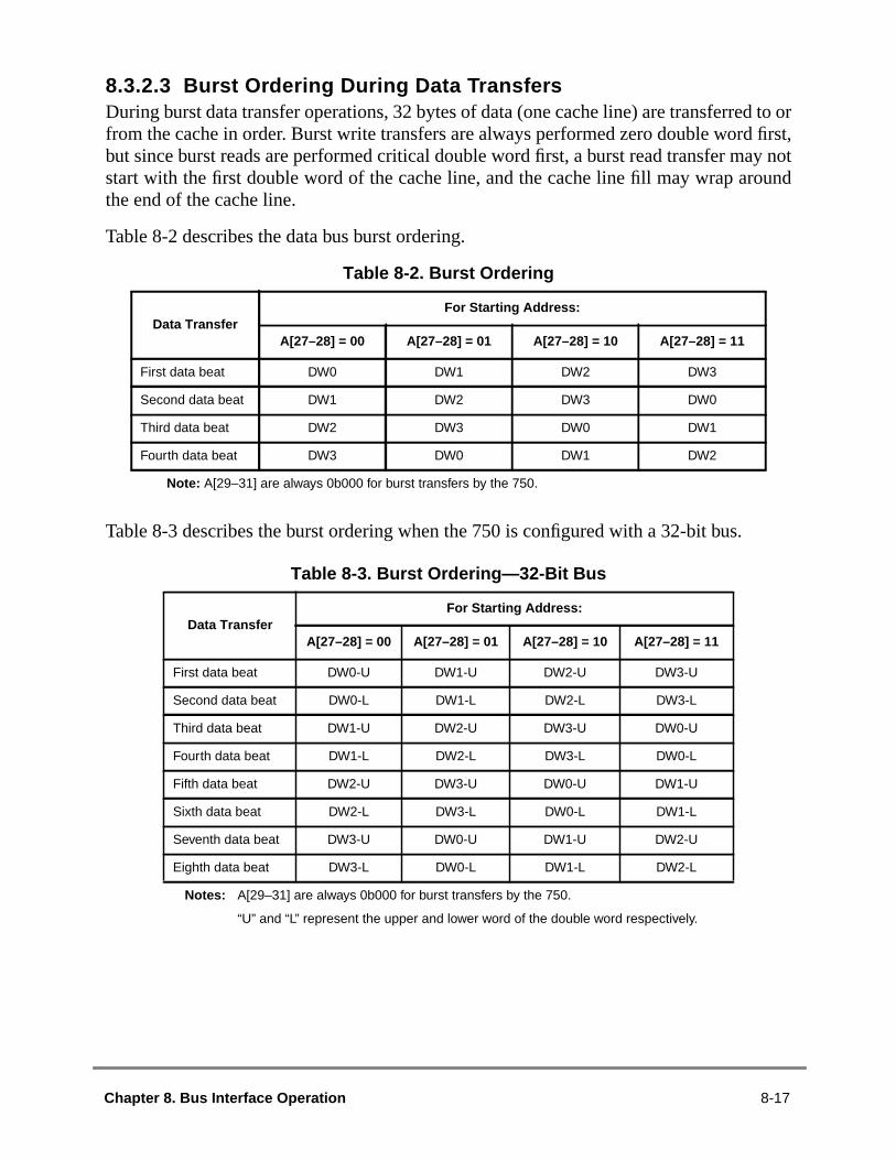
d to orfirst,
ay notund
8.3.2.3 Burst Ordering During Data TransfersDuring burst data transfer operations, 32 bytes of data (one cache line) are transferrefrom the cache in order. Burst write transfers are always performed zero double wordbut since burst reads are performed critical double word first, a burst read transfer mstart with the first double word of the cache line, and the cache line fill may wrap arothe end of the cache line.
Table 8-2 describes the data bus burst ordering.
Table 8-3 describes the burst ordering when the 750 is configured with a 32-bit bus.
Table 8-2. Burst Ordering
Data TransferFor Starting Address:
A[27–28] = 00 A[27–28] = 01 A[27–28] = 10 A[27–28] = 11
First data beat DW0 DW1 DW2 DW3
Second data beat DW1 DW2 DW3 DW0
Third data beat DW2 DW3 DW0 DW1
Fourth data beat DW3 DW0 DW1 DW2
Note: A[29–31] are always 0b000 for burst transfers by the 750.
Table 8-3. Burst Ordering—32-Bit Bus
Data TransferFor Starting Address:
A[27–28] = 00 A[27–28] = 01 A[27–28] = 10 A[27–28] = 11
First data beat DW0-U DW1-U DW2-U DW3-U
Second data beat DW0-L DW1-L DW2-L DW3-L
Third data beat DW1-U DW2-U DW3-U DW0-U
Fourth data beat DW1-L DW2-L DW3-L DW0-L
Fifth data beat DW2-U DW3-U DW0-U DW1-U
Sixth data beat DW2-L DW3-L DW0-L DW1-L
Seventh data beat DW3-U DW0-U DW1-U DW2-U
Eighth data beat DW3-L DW0-L DW1-L DW2-L
Notes: A[29–31] are always 0b000 for burst transfers by the 750.
“U” and “L” represent the upper and lower word of the double word respectively.
Chapter 8. Bus Interface Operation 8-17

fers indata.-byte
ntiallyned toress).
moryworde 8-5ross aple, arosses
8.3.2.4 Effect of Alignment in Data TransfersTable 8-4 lists the aligned transfers that can occur on the 750 bus. These are transwhich the data is aligned to an address that is an integral multiple of the size of theFor example, Table 8-4 shows that 1-byte data is always aligned; however, for a 4word to be aligned, it must be oriented on an address that is a multiple of 4.
The 750 supports misaligned memory operations, although their use may substadegrade performance. Misaligned memory transfers address memory that is not aligthe size of the data being transferred (such as, a word read of an odd byte addAlthough most of these operations hit in the primary cache (or generate burst meoperations if they miss), the 750 interface supports misaligned transfers within a(32-bit aligned) boundary, as shown in Table 8-5. Note that the 4-byte transfer in Tablis only one example of misalignment. As long as the attempted transfer does not cword boundary, the 750 can transfer the data on the misaligned address (for examhalf-word read from an odd byte-aligned address). An attempt to address data that ca word boundary requires two bus transfers to access the data.
Table 8-4. Aligned Data Transfers
Transfer Size TSIZ0 TSIZ1 TSIZ2 A[29–31]Data Bus Byte Lane(s)
0 1 2 3 4 5 6 7
Byte 0 0 1 000 — — — — — — —
0 0 1 001 — — — — — — —
0 0 1 010 — — — — — — —
0 0 1 011 — — — — — — —
0 0 1 100 — — — — — — —
0 0 1 101 — — — — — — —
0 0 1 110 — — — — — — —
0 0 1 111 — — — — — — —
Half word 0 1 0 000 — — — — — —
0 1 0 010 — — — — — —
0 1 0 100 — — — — — —
0 1 0 110 — — — — — —
Word 1 0 0 000 — — — —
1 0 0 100 — — — —
Double word 0 0 0 000
Notes: These entries indicate the byte portions of the requested operand that are read or written duringthat bus transaction.These entries are not required and are ignored during read transactions and are driven with unde-fined data during all write transactions.
8-18 IBM PowerPC 740 / PowerPC 750 RISC Microprocessor User’s Manual

s, theydressultipled that
of thet foreratedAll
Due to the performance degradations associated with misaligned memory operationare best avoided. In addition to the double-word straddle boundary condition, the adtranslation logic can generate substantial exception overhead when the load/store mand load/store string instructions access misaligned data. It is strongly recommendesoftware attempt to align data where possible.
8.3.2.4.1 Effect of Alignment in Data Transfers (32-Bit Bus)The aligned data transfer cases for 32-bit data bus mode are shown in Table 8-6. Alltransfers require a single data beat (if caching-inhibited or write-through) excepdouble-word cases which require two data beats. The double-word case is only genby the 750 for load or store double operations to/from the floating-point GPRs.caching-inhibited instruction fetches are performed as word operations.
Table 8-5. Misaligned Data Transfers (Four-Byte Examples)
Transfer Size(Four Bytes)
TSIZ[0–2] A[29–31]Data Bus Byte Lanes
0 1 2 3 4 5 6 7
Aligned 1 0 0 0 0 0 A A A A — — — —
Misaligned—first access
second access
0 1 1 0 0 1 A A A — — — —
0 0 1 1 0 0 — — — — A — — —
Misaligned—first access
second access
0 1 0 0 1 0 — — A A — — — —
0 1 1 1 0 0 — — — — A A — —
Misaligned—first access
second access
0 0 1 0 1 1 — — — A — — — —
0 1 1 1 0 0 — — — — A A A —
Aligned 1 0 0 1 0 0 — — — — A A A A
Misaligned—first access
second access
0 1 1 1 0 1 — — — — — A A A
0 0 1 0 0 0 A — — — — — — —
Misaligned—first access
second access
0 1 0 1 1 0 — — — — — — A A
0 1 0 0 0 0 A A — — — — — —
Misaligned—first access
second access
0 0 1 1 1 1 — — — — — — — A
0 1 1 0 0 0 A A A — — — — —
Notes:
A: Byte lane used—: Byte lane not used
Chapter 8. Bus Interface Operation 8-19

in they thensfer
Misaligned data transfers when the 750 is configured with a 32-bit data bus operatesame way as when configured with a 64-bit data bus, with the exception that onlDH[0–31] data bus is used. See Table 8-7 for an example of a 4-byte misaligned trastarting at each possible byte address within a double word.
Table 8-6. Aligned Data Transfers (32-Bit Bus Mode)
Transfer Size TSIZ0 TSIZ1 TSIZ2 A[29–31]Data Bus Byte Lane(s)
0 1 2 3 4 5 6 7
Byte 0 0 1 000 A — — — x x x x
0 0 1 001 — A x — x x x x
0 0 1 010 — — A — x x x x
0 0 1 011 — — — A x x x x
0 0 1 100 A — — — x x x x
0 0 1 101 — A — — x x x x
0 0 1 110 — — A — x x x x
0 0 1 111 — — — A x x x x
Half word 0 1 0 000 A A — — x x x x
0 1 0 010 — — A A x x x x
0 1 0 100 A A — — x x x x
0 1 0 110 — — A A x x x x
Word 1 0 0 000 A A A A x x x x
1 0 0 100 A A A A x x x x
Double word
Second beat
0 0 0 000 A A A A x x x x
0 0 0 000 A A A A x x x x
Notes:
A: Byte lane used—: Byte lane not usedx: Byte lane not used in 32-bit bus mode
8-20 IBM PowerPC 740 / PowerPC 750 RISC Microprocessor User’s Manual

the
tion ofsscan
hesecycle,
8.3.2.5 Alignment of External Control InstructionsThe size of the data transfer associated with theeciwx andecowx instructions is always4 bytes. If theeciwxor ecowxinstruction is misaligned and crosses any word boundary,750 will generate an alignment exception.
8.3.3 Address Transfer TerminationThe address tenure of a bus operation is terminated when completed with the asserAACK, or retried with the assertion ofARTRY. The 750 does not terminate the addretransfer until theAACK (address acknowledge) input is asserted; therefore, the systemextend the address transfer phase by delaying the assertion ofAACK to the 750. Theassertion ofAACK can be as early as the bus clock cycle followingTS (see Figure 8-8),which allows a minimum address tenure of two bus cycles. As shown in Figure 8-8, tsignals are asserted for one bus clock cycle, three-stated for half of the next bus clockdriven high till the following bus cycle, and finally three-stated. Note thatAACK must beasserted for only one bus clock cycle.
Table 8-7. Misaligned 32-Bit Data Bus Transfer (Four-Byte Examples)
Transfer Size(Four Bytes)
TSIZ[0–2] A[29–31]Data Bus Byte Lanes
0 1 2 3 4 5 6 7
Aligned 1 0 0 0 0 0 A A A A x x x x
Misaligned—first access
second access
0 1 1 0 0 1 A A A x x x x
0 0 1 1 0 0 A — — — x x x x
Misaligned—first access
second access
0 1 0 0 1 0 — — A A x x x x
0 1 0 1 0 0 A A — x x x x x
Misaligned—first access
second access
0 0 1 0 1 1 — — — A x x x x
0 1 1 1 0 0 A A A — x x x x
Aligned 1 0 0 1 0 0 A A A A x x x x
Misaligned—first access
second access
0 1 1 1 0 1 — A A A x x x x
0 0 1 0 0 0 A — — — x x x x
Misaligned—first access
second access
0 1 0 1 1 0 — — A A x x x x
0 1 0 0 0 0 A A — — x x x x
Misaligned—first access
second access
0 0 1 1 1 1 — — — A x x x x
0 1 1 0 0 0 A A A — x x x x
Notes:
A: Byte lane used—: Byte lane not usedx: Byte lane not used in 32-bit bus mode
Chapter 8. Bus Interface Operation 8-21

device,cheiced.
e next
ng
begun,s beenstit isits. If
hatssertthe busarbiter
bus
bitergtenuresn alsos are
The address transfer can be terminated with the requirement to retry ifARTRY is assertedanytime during the address tenure and through the cycle followingAACK. The assertioncauses the entire transaction (address and data tenure) to be rerun. As a snoopingthe 750 assertsARTRY for a snooped transaction that hits modified data in the data cathat must be written back to memory, or if the snooped transaction could not be servAs a bus master, the 750 responds to an assertion ofARTRY by aborting the bus transactionand re-requesting the bus. Note that after recognizing an assertion ofARTRY and abortingthe transaction in progress, the 750 is not guaranteed to run the same transaction thtime it is granted the bus due to internal reordering of load and store operations.
If an address retry is required, theARTRY response will be asserted by a bus snoopidevice as early as the second cycle after the assertion ofTS. Once asserted,ARTRY mustremain asserted through the cycle after the assertion ofAACK. The assertion ofARTRYduring the cycle after the assertion ofAACK is referred to as a qualifiedARTRY. An earlierassertion ofARTRY during the address tenure is referred to as an earlyARTRY.
As a bus master, the 750 recognizes either an early or qualifiedARTRY and prevents thedata tenure associated with the retried address tenure. If the data tenure has alreadythe 750 aborts and terminates the data tenure immediately even if the burst data hareceived. If the assertion ofARTRY is received up to or on the bus cycle following the fir(or only) assertion ofTA for the data tenure, the 750 ignores the first data beat, and ifa load operation, does not forward data internally to the cache and execution unARTRY is asserted after the first (or only) assertion ofTA, improper operation of the businterface may result.
During the clock of a qualifiedARTRY, the 750 also determines if it should negateBR andignoreBG on the following cycle. On the following cycle, only the snooping master tassertedARTRY and needs to perform a snoop copy-back operation is allowed to aBR. This guarantees the snooping master an opportunity to request and be grantedbefore the just-retried master can restart its transaction. Note that a nonclocked busmay detect the assertion of address bus request by the bus master that assertedARTRY, andreturn a qualified bus grant one cycle earlier than shown in Figure 8-8.
Note that if the 750 assertsARTRY due to a snoop operation, and assertsBR in the buscycle followingARTRY in order to perform a snoop push to memory it may be severalcycles later before the 750 will be able to accept aBG. (The delay in responding to theassertion ofBG only occurs during snoop pushes from the L2 cache.) The bus arshould keepBG asserted until it detectsBR negated orTS asserted from the 750 indicatinthat the snoop copy-back has begun. The system should ensure that no other addressoccur until the current snoop push from the 750 is completed. Snoop push delays cabe avoided by operating the L2 cache in write-through mode so no snoop pusherequired by the L2 cache.
8-22 IBM PowerPC 740 / PowerPC 750 RISC Microprocessor User’s Manual

ned bye of the
us
is an. If the
Figure 8-8. Snooped Address Cycle with ARTRY
8.4 Data Bus TenureThis section describes the data bus arbitration, transfer, and termination phases defithe 750 memory access protocol. The phases of the data tenure are identical to thosaddress tenure, underscoring the symmetry in the control of the two buses.
8.4.1 Data Bus ArbitrationData bus arbitration uses the data arbitration signal group—DBG, DBWO, andDBB.Additionally, the combination ofTS and TT[0–4] provides information about the data brequest to external logic.
TheTS signal is an implied data bus request from the 750; the arbiter must qualifyTS withthe transfer type (TT) encodings to determine if the current address transferaddress-only operation, which does not require a data bus transfer (see Figure 8-8)data bus is needed, the arbiter grants data bus mastership by asserting theDBG input to the750. As with the address bus arbitration phase, the 750 must qualify theDBG input with anumber of input signals before assuming bus mastership, as shown in Figure 8-9.
1 2 3 4 5 6 7
ts
abb
addr
aack
ARTRY
BR
qualBG
ABB
8
Chapter 8. Bus Interface Operation 8-23

ership
e mayIn this
left torectly
if the
therting it
rnta
Figure 8-9. Data Bus Arbitration
A qualified data bus grant can be expressed as the following:
QDBG =DBG asserted whileDBB, DRTRY, andARTRY (associated with the databus operation) are negated.
When a data tenure overlaps with its associated address tenure, a qualifiedARTRYassertion coincident with a data bus grant signal does not result in data bus mast(DBB is not asserted). Otherwise, the 750 always assertsDBB on the bus clock cycle afterrecognition of a qualified data bus grant. Since the 750 can pipeline transactions, therbe an outstanding data bus transaction when a new address transaction is retried.case, the 750 becomes the data bus master to complete the previous transaction.
8.4.1.1 Using the DBB SignalTheDBB signal should be connected between masters if data tenure scheduling isthe masters. Optionally, the memory system can control data tenure scheduling diwith DBG. However, it is possible to ignore theDBB signal in the system if theDBB inputis not used as the final data bus allocation control between data bus masters, andmemory system can track the start and end of the data tenure. IfDBB is not used to signalthe end of a data tenure,DBG is only asserted to the next bus master the cycle beforecycle that the next bus master may actually begin its data tenure, rather than asseearlier (usually during another master’s data tenure) and allowing the negation ofDBB tobe the final gating signal for a qualified data bus grant. Even ifDBB is ignored in thesystem, the 750 always recognizes its own assertion ofDBB, and requires one cycle aftedata tenure completion to negate its ownDBB before recognizing a qualified data bus grafor another data tenure. IfDBB is ignored in the system, it must still be connected topull-up resistor on the 750 to ensure proper operation.
0 1 2 3
TS
dbg
dbb
drtry
qual DBG
DBB
8-24 IBM PowerPC 740 / PowerPC 750 RISC Microprocessor User’s Manual

ed toedwever,
been
erform
bus to
) tos,a
oryns.
ationsEffectare
higher
ta isroughpportle (andtake
e- orofns thatMU),ta thato beburst
8.4.2 Data Bus Write OnlyAs a result of address pipelining, the 750 may have up to two data tenures queuperform when it receives a qualifiedDBG. Generally, the data tenures should be performin strict order (the same order) as their address tenures were performed. The 750, hoalso supports a limited out-of-order capability with the data bus write only (DBWO) input.When recognized on the clock of a qualifiedDBG, DBWO may direct the 750 to performthe next pending data write tenure even if a pending read tenure would have normallyperformed first. For more information on the operation ofDBWO, refer to Section 8.10,“Using Data Bus Write Only.”
If the 750 has any data tenures to perform, it always accepts data bus mastership to pa data tenure when it recognizes a qualifiedDBG. If DBWO is asserted with a qualifiedDBG and no write tenure is queued to run, the 750 still takes mastership of the dataperform the next pending read data tenure.
Generally,DBWO should only be used to allow a copy-back operation (burst writeoccur before a pending read operation. IfDBWO is used for single-beat write operationit may negate the effect of theeieio instruction by allowing a write operation to precedeprogram-scheduled read operation.
8.4.3 Data TransferThe data transfer signals include DH[0–31], DL[0–31], and DP[0–7]. For memaccesses, the DH and DL signals form a 64-bit data path for read and write operatio
The 750 transfers data in either single- or four-beat burst transfers. Single-beat opercan transfer from 1 to 8 bytes at a time and can be misaligned; see Section 8.3.2.4, “of Alignment in Data Transfers.” Burst operations always transfer eight words andaligned on eight-word address boundaries. Burst transfers can achieve significantlybus throughput than single-beat operations.
The type of transaction initiated by the 750 depends on whether the code or dacacheable and, for store operations whether the cache is in write-back or write-thmode, which software controls on either a page or block basis. Burst transfers sucacheable operations only; that is, memory structures must be marked as cacheabwrite-back for data store operations) in the respective page or block descriptor toadvantage of burst transfers.
The 750 outputTBST indicates to the system whether the current transaction is a singlfour-beat transfer (except duringeciwx/ecowx transactions, when it signals the stateEAR[28]). A burst transfer has an assumed address order. For load or store operatiomiss in the cache (and are marked as cacheable and, for stores, write-back in the Mthe 750 uses the double-word-aligned address associated with the critical code or dainitiated the transaction. This minimizes latency by allowing the critical code or data tforwarded to the processor before the rest of the cache line is filled. For all other
Chapter 8. Bus Interface Operation 8-25

igned
fta that
a isusertede
ation
st ther the
.
t may
lybeenof
n the
,
fer
operations, however, the cache line is transferred beginning with the eight-word-aldata.
8.4.4 Data Transfer TerminationFour signals are used to terminate data bus transactions—TA, DRTRY (data retry),TEA(transfer error acknowledge), andARTRY. TheTA signal indicates normal termination odata transactions. It must always be asserted on the bus cycle coincident with the dait is qualifying. It may be withheld by the slave for any number of clocks until valid datready to be supplied or accepted.DRTRY indicates invalid read data in the previous bclock cycle.DRTRY extends the current data beat and does not terminate it. If it is assafter the last (or only) data beat, the 750 negatesDBB but still considers the data beat activand waits for another assertion ofTA. DRTRY is ignored on write operations.TEAindicates a nonrecoverable bus error event. Upon receiving a final (or only) termincondition, the 750 always negatesDBB for one cycle.
If DRTRY is asserted by the memory system to extend the last (or only) data beat panegation ofDBB, the memory system should three-state the data bus on the clock aftefinal assertion ofTA, even though it will negateDRTRY on that clock. This is to prevent apotential momentary data bus conflict if a write access begins on the following cycle
TheTEA signal is used to signal a nonrecoverable error during the data transaction. Ibe asserted on any cycle duringDBB, or on the cycle after a qualifiedTA during a readoperation, except when no-DRTRY mode is selected (where no-DRTRY mode cancelschecking the cycle afterTA). The assertion ofTEA terminates the data tenure immediateeven if in the middle of a burst; however, it does not prevent incorrect data that has justacknowledged withTA from being written into the 750’s cache or GPRs. The assertionTEA initiates either a machine check exception or a checkstop condition based osetting of the MSR[ME] bit.
An assertion ofARTRY causes the data tenure to be terminated immediately if theARTRYis for the address tenure associated with the data tenure in operation. IfARTRY isconnected for the 750, the earliest allowable assertion ofTA to the 750 is directlydependent on the earliest possible assertion ofARTRY to the 750; see Section 8.3.3“Address Transfer Termination.”
8.4.4.1 Normal Single-Beat TerminationNormal termination of a single-beat data read operation occurs whenTA is asserted by aresponding slave. TheTEA andDRTRY signals must remain negated during the trans(see Figure 8-10).
8-26 IBM PowerPC 740 / PowerPC 750 RISC Microprocessor User’s Manual

Figure 8-10. Normal Single-Beat Read Termination
TheDRTRY signal is not sampled during data writes, as shown in Figure 8-11.
Figure 8-11. Normal Single-Beat Write Termination
0 1 2 3 4
TS
qual DBG
DBB
data
ta
drtry
AACK
0 1 2 3
TS
qual DBG
DBB
data
ta
drtry
AACK
Chapter 8. Bus Interface Operation 8-27

,
inatests,.
onat cand
tion of
se the
even
Normal termination of a burst transfer occurs whenTA is asserted for four bus clock cyclesas shown in Figure 8-12. The bus clock cycles in whichTA is asserted need not beconsecutive, thus allowing pacing of the data transfer beats. For read bursts to termsuccessfully,TEA andDRTRY must remain negated during the transfer. For write burTEA must remain negated for a successful transfer.DRTRY is ignored during data writes
Figure 8-12. Normal Burst Transaction
For read bursts,DRTRY may be asserted one bus clock cycle afterTA is asserted to signalthat the data presented withTA is invalid and that the processor must wait for the negatiof DRTRY before forwarding data to the processor (see Figure 8-13). Thus, a data bebe terminated by a predicted branch withTA and then one bus clock cycle later confirmewith the negation ofDRTRY. TheDRTRY signal is valid only for read transactions.TAmust be asserted on the bus clock cycle before the first bus clock cycle of the asserDRTRY; otherwise the results are undefined.
TheDRTRY signal extends data bus mastership such that other processors cannot udata bus untilDRTRY is negated. Therefore, in the example in Figure 8-13,DBB cannotbe asserted until bus clock cycle 6. This is true for both read and write operationsthoughDRTRY does not extend bus mastership for write operations.
1 2 3 4 5 6 7
TS
qual DBG
DBB
data
ta
drtry
8-28 IBM PowerPC 740 / PowerPC 750 RISC Microprocessor User’s Manual

ct-14,til bus
uchn the
Figure 8-13. Termination with DRTRY
Figure 8-14 shows the effect of usingDRTRY during a burst read. It also shows the effeof usingTA to pace the data transfer rate. Notice that in bus clock cycle 3 of Figure 8TA is negated for the second data beat. The 750 data pipeline does not proceed unclock cycle 4 when theTA is reasserted.
Figure 8-14. Read Burst with TA Wait States and DRTRY
Note thatDRTRY is useful for systems that implement predicted forwarding of data sas those with direct-mapped, third-level caches where hit/miss is determined ofollowing bus clock cycle, or for parity- or ECC-checked memory systems.
Note thatDRTRY may not be implemented on other PowerPC processors.
1 2 3 4 5
TS
qual DBG
DBB
data
ta
drtry
TS
qual DBG
DBB
data
ta
drtry
1 2 3 4 5 6 7 8 9
Chapter 8. Bus Interface Operation 8-29

stopon isd or atpting. It ises thetermst bed. Todresserrorsavedtion ofater).he.tcause
icate).
plete.
mustens to
ringdition
g buserency
oped
an onehen
8.4.4.2 Data Transfer Termination Due to a Bus ErrorTheTEA signal indicates that a bus error occurred. It may be asserted whileDBB (and/orDRTRY for read operations) is asserted. AssertingTEA to the 750 terminates thetransaction; that is, further assertions ofTA andDRTRY are ignored andDBB is negated.
Assertion of theTEA signal causes a machine check exception (and possibly a checkcondition within the 750). For more information, see Section , “The hard reset exceptia nonrecoverable, nonmaskable asynchronous exception. When HRESET is assertepower-on reset (POR), the 750 immediately branches to 0xFFF0_0100 without attemto reach a recoverable state. A hard reset has the highest priority of any exceptionalways nonrecoverable. Table 4-9 shows the state of the machine just before it fetchfirst instruction of the system reset handler after a hard reset. In Table 4-9, the“Unknown” means that the content may have been disordered. These facilities muproperly initialized before use. The FPRs, BATs, and TLBs may have been disordereinitialize the BATs, first set them all to zero, then to the correct values before any adtranslation occurs..” Note also that the 750 does not implement a synchronouscapability for memory accesses. This means that the exception instruction pointerinto the SRR0 register does not point to the memory operation that caused the asserTEA, but to the instruction about to be executed (perhaps several instructions lHowever, assertion ofTEA does not invalidate data entering the GPR or the cacAdditionally, the address corresponding to the access that causedTEA to be asserted is nolatched by the 750. To recover, the exception handler must determine and remedy theof theTEA, or the 750 must be reset; therefore, this function should only be used to indfatal system conditions to the processor (such as parity or uncorrectable ECC errors
After the 750 has committed to run a transaction, that transaction must eventually comAddress retry causes the transaction to be restarted;TA wait states andDRTRY assertionfor reads delay termination of individual data beats. Eventually, however, the systemeither terminate the transaction or assert theTEA signal. For this reason, care must be takto check for the end of physical memory and the location of certain system facilitieavoid memory accesses that result in the assertion ofTEA.
Note thatTEA generates a machine check exception depending on MSR[ME]. Cleathe machine check exception enable control bits leads to a true checkstop con(instruction execution halted and processor clock stopped).
8.4.5 Memory Coherency—MEI ProtocolThe 750 provides dedicated hardware to provide memory coherency by snoopintransactions. The address retry capability enforces the three-state, MEI cache-cohprotocol (see Figure 8-15).
The global (GBL) output signal indicates whether the current transaction must be snoby other snooping devices on the bus. Address bus masters assertGBL to indicate that thecurrent transaction is a global access (that is, an access to memory shared by more thdevice). IfGBL is not asserted for the transaction, that transaction is not snooped. W
8-30 IBM PowerPC 740 / PowerPC 750 RISC Microprocessor User’s Manual

cast
thee theevious
nopingis not
wever,wn inand
other devices detect theGBL input asserted, they must respond by snooping the broadaddress.
Normally, GBL reflects the M bit value specified for the memory reference incorresponding translation descriptor(s). Note that care must be taken to minimiznumber of pages marked as global, because the retry protocol discussed in the prsection is used to enforce coherency and can require significant bus bandwidth.
When the 750 is not the address bus master,GBL is an input. The 750 snoops a transactioif TS andGBL are asserted together in the same bus clock cycle (this is a qualified snocondition). No snoop update to the 750 cache occurs if the snooped transactionmarked global. This includes invalidation cycles.
When the 750 detects a qualified snoop condition, the address associated with theTS iscompared against the data cache tags. Snooping completes if no hit is detected. If, hothe address hits in the cache, the 750 reacts according to the MEI protocol shoFigure 8-15, assuming the WIM bits are set to write-back, caching-allowed,coherency-enforced modes (WIM = 001).
Chapter 8. Bus Interface Operation 8-31

Figure 8-15. MEI Cache Coherency Protocol—State Diagram (WIM = 001)
BUS TRANSACTIONS
SH =Snoop Hit = Snoop PushRH =Read HitWH =Write Hit = Cache Line FillWM=Write MissRM =Read MissSH/CRW=Snoop Hit, Cacheable Read/WriteSH/CIR =Snoop Hit, Caching-Inhibited Read
RH
WH
RH
MODIFIEDWH
SH
SH/CIR
SH/CRW
WM
EXCLUSIVE
INVALID
SH/CRW
RM
8-32 IBM PowerPC 740 / PowerPC 750 RISC Microprocessor User’s Manual

astestandases,
ss the
8.5 Timing ExamplesThis section shows timing diagrams for various scenarios. Figure 8-16 illustrates the fsingle-beat reads possible for the 750. This figure shows both minimal latencymaximum single-beat throughput. By delaying the data bus tenure, the latency increbut, because of split-transaction pipelining, the overall throughput is not affected unledata bus latency causes the third address tenure to be delayed.
Note that all bidirectional signals are three-stated between bus tenures.
Figure 8-16. Fastest Single-Beat Reads
BR
BG
ABB
TS
A[0–31]
TT[0–4]
TBST
GBL
AACK
ARTRY
DBG
DBB
D[0–63]
TA
DRTRY
TEA
1 2 3 4 5 6 7 8 9 10 11 12
1 2 3 4 5 6 7 8 9 10 11 12
CPU A CPU A CPU A
Read Read Read
In In In
Chapter 8. Bus Interface Operation 8-33

ional
Figure 8-17 illustrates the fastest single-beat writes supported by the 750. All bidirectsignals are three-stated between bus tenures.Figure 8-17. Fastest Single-Beat Writes
BR
BG
ABB
TS
A[0–31]
TT[0–4]
TBST
GBL
AACK
ARTRY
DBG
DBB
D[0–63]
TA
DRTRY
TEA
1 2 3 4 5 6 7 8 9 10 11 12
1 2 3 4 5 6 7 8 9 10 11 12
CPU A CPU A CPU A
SBW SBW SBW
Out Out Out
8-34 IBM PowerPC 740 / PowerPC 750 RISC Microprocessor User’s Manual

ls:
.
ta.
liningle, an
Figure 8-18 shows three ways to delay single-beat reads showing data-delay contro
• TheTA signal can remain negated to insert wait states in clock cycles 3 and 4• For the second access,DBG could have been asserted in clock cycle 6.• In the third access,DRTRY is asserted in clock cycle 11 to flush the previous da
Note that all bidirectional signals are three-stated between bus tenures. The pipeshown in Figure 8-18 can occur if the second access is not another load (for exampinstruction fetch).
Figure 8-18. Single-Beat Reads Showing Data-Delay Controls
BR
BG
ABB
TS
A[0–31]
TT[0–4]
TBST
GBL
AACK
ARTRY
DBG
DBB
D[0–63]
TA
DRTRY
TEA
CPU A CPU A CPU A
Read Read Read
In In Bad
1 2 3 4 5 6 7 8 9 10 11 12 13 14
1 2 3 4 5 6 7 8 9 10 11 12 13 14
In
Chapter 8. Bus Interface Operation 8-35

t alld in the
Figure 8-19 shows data-delay controls in a single-beat write operation. Note thabidirectional signals are three-stated between bus tenures. Data transfers are delayefollowing ways:
• TheTA signal is held negated to insert wait states in clocks 3 and 4.• In clock 6,DBG is held negated, delaying the start of the data tenure.
The last access is not delayed (DRTRY is valid only for read operations).
Figure 8-19. Single-Beat Writes Showing Data Delay Controls
BR
BG
ABB
TS
A[0–31]
TT[0–4]
TBST
GBL
AACK
ARTRY
DBG
DBB
D[0–63]
TA
DRTRY
TEA
1 2 3 4 5 6 7 8 9 10 11 12
1 2 3 4 5 6 7 8 9 10 11 12
CPU A CPU A CPU A
SBW SBW SBW
Out Out Out
8-36 IBM PowerPC 740 / PowerPC 750 RISC Microprocessor User’s Manual

t all
Figure 8-20 shows the use of data-delay controls with burst transfers. Note thabidirectional signals are three-stated between bus tenures. Note the following:• The first data beat of bursted read data (clock 0) is the critical quad word.• The write burst shows the use ofTA signal negation to delay the third data beat.• The final read burst shows the use ofDRTRY on the third data beat.• The address for the third transfer is delayed until the first transfer completes.
Figure 8-20. Burst Transfers with Data Delay Controls
BR
BG
ABB
TS
A[0–31]
TT[0–4]
TBST
GBL
AACK
ARTRY
DBG
DBB
D[0–63]
TA
DRTRY
TEA
CPU A
In 0
1 2 3 4 5 6 7 8 9 10 11 12 13 14 15 16 17 18 19 20
1 2 3 4 5 6 7 8 9 10 11 12 13 14 15 16 17 18 19 20
CPU A CPU A
Read Write Read
In 1 In 2 In 3 Out 0 Out 1 Out 2 Out 3 In 0 In 1 In 2 In 3In 2
Chapter 8. Bus Interface Operation 8-37

e
Figure 8-21 shows the use of theTEA signal. Note that all bidirectional signals arthree-stated between bus tenures. Note the following:• The first data beat of the read burst (in clock 0) is the critical quad word.
• TheTEA signal truncates the burst write transfer on the third data beat.
• The 750 eventually causes an exception to be taken on theTEA event.
Figure 8-21. Use of Transfer Error Acknowledge ( TEA)
BR
BG
ABB
TS
A[0–31]
TT[0–4]
TBST
GBL
AACK
ARTRY
DBG
DBB
D[0–63]
TA
DRTRY
TEA
CPU A
In 0
1 2 3 4 5 6 7 8 9 10 11 12 13 14 15 16 17
CPU A CPU A
Read Write Read
In 1 In 2 In 3 Out 0 Out 1 Out 2 In 0 In 1 In 3In 2
1 2 3 4 5 6 7 8 9 10 11 12 13 14 15 16 17
8-38 IBM PowerPC 740 / PowerPC 750 RISC Microprocessor User’s Manual

of theribed
tes thein themode,Byteode.
nd they
e, two,for theibited
s arens arefor a. All
nto ore way2
s and. Late
eat ister
hown
8.6 Optional Bus ConfigurationThe 750 supports optional bus configurations that is selected during the negationHRESET signal. The operation and selection of the optional bus configuration is descin the following sections.
8.6.1 32-Bit Data Bus ModeThe 750 supports an optional 32-bit data bus mode. The 32-bit data bus mode operasame as the 64-bit data bus mode with the exception of the byte lanes involvedtransfer and the number of data beats that are performed. When in 32-bit data busonly byte lanes 0 through 3 are used corresponding to DH0–DH31 and DP0–DP3.lanes 4 through 7 corresponding to DL0–DL31 and DP4–DP7 are never used in this mThe unused data bus signals are not sampled by the 750 during read operations, aare driven low during write operations.
The number of data beats required for a data tenure in the 32-bit data bus mode is onor eight beats depending on the size of the program transaction and the cache modeaddress. Data transactions of one or two data beats are performed for caching-inhload/store or write-through store operations. These transactions do not assert theTBSTsignal even though a two-beat burst may be performed (having the sameTBST andTSIZ[0–2] encodings as the 64-bit data bus mode). Single-beat data transactionperformed for bus operations of 4 bytes or less, and double-beat data transactioperformed for 8-byte operations only. The 750 only generates an 8-byte operationdouble-word-aligned load or store double operation to or from the floating-point GPRscache-inhibited instruction fetches are performed as word (single-beat) operations.
Data transactions of eight data beats are performed for burst operations that load istore from the 750’s internal caches. These transactions transfer 32 bytes in the samas in 64-bit data bus mode, asserting theTBST signal, and signaling a transfer size of(TSIZ(0–2) = 0b010).
The same bus protocols apply for arbitration, transfer, and termination of the addresdata tenures in the 32-bit data bus mode as they apply to the 64-bit data bus modeARTRY cancellation of the data tenure applies on the bus clock after the first data backnowledged (after the firstTA) for word or smaller transactions, or on the bus clock afthe second data beat is acknowledged (after the secondTA) for double-word or burstoperations (or coincident with respectiveTA if no-DRTRY mode is selected).
An example of an eight-beat data transfer while the 750 is in 32-bit data bus mode is sin Figure 8-22.
Chapter 8. Bus Interface Operation 8-39

is
of the
Figure 8-22. 32-Bit Data Bus Transfer (Eight-Beat Burst)
An example of a two-beat data transfer (withDRTRY asserted during each data tenure)shown in Figure 8-23.
Figure 8-23. 32-Bit Data Bus Transfer (Two-Beat Burst with DRTRY)
The 750 selects 64-bit or 32-bit data bus mode at startup by sampling the stateTLBISYNC signal at the negation ofHRESET. If theTLBISYNC signal is negated at the
TS
ABB
ADDR
TBST
AACK
ARTRY
DBB
DH[0–31]
TA
DRTRY
TEA
0 1 2 3 4 5 6 7
TS
ABB
ADDR
TBST
AACK
ARTRY
DBB
DH[0–31]
TA
DRTRY
TEA
0 1
Chapter 8. Bus Interface Operation 8-40

videdgtocol.
mally
holdata isthe
the
r it
ration
after
the
rface.re
terr bus
negation ofHRESET, 64-bit data mode is entered by the 750. IfTLBISYNC is asserted atthe negation ofHRESET, 32-bit data mode is entered.
8.6.2 No-DRTRY ModeThe 750 supports an optional mode to disable the use of the data retry function prothrough theDRTRY signal. The no-DRTRY mode allows the forwarding of data durinload operations to the internal CPU one bus cycle sooner than in the normal bus pro
The 60x bus protocol specifies that, during load operations, the memory system norhas the capability to cancel data that was read by the master on the bus cycle afterTA wasasserted. In the 750 implementation, this late cancellation protocol requires the 750 toany loaded data at the bus interface for one additional bus clock to verify that the dvalid before forwarding it to the internal CPU. For systems that do not implementDRTRY function, the 750 provides an optional no-DRTRY mode that eliminates thisone-cycle stall during all load operations, and allows for the forwarding of data tointernal CPU immediately whenTA is recognized.
When the 750 is in the no-DRTRY mode, data can no longer be cancelled the cycle afteis acknowledged by an assertion ofTA. Data is immediately forwarded to the CPUinternally, and any attempt at late cancellation by the system may cause improper opeby the 750.
When the 750 is following normal bus protocol, data may be cancelled the bus cycleTA by either of two means—late cancellation byDRTRY, or late cancellation byARTRY.When no-DRTRY mode is selected, both cancellation cases must be disallowed insystem design for the bus protocol.
When no-DRTRY mode is selected for the 750, the system must ensure thatDRTRY is notasserted to the 750. If it is asserted, it may cause improper operation of the bus inteThe system must also ensure that an assertion ofARTRY by a snooping device must occubefore or coincident with the first assertion ofTA to the 750, but not on the cycle after thfirst assertion ofTA.
Other than the inability to cancel data that was read by the master on the bus cycle afTAwas asserted, the bus protocol for the 750 is identical to that for the basic transfeprotocols described in this chapter, including 32-bit data bus mode.
The 750 selects the desiredDRTRY mode at startup by sampling the state of theDRTRYsignal itself at the negation of theHRESET signal. If theDRTRY signal is negated at thenegation ofHRESET, normal operation is selected. If theDRTRY signal is asserted at thenegation ofHRESET, no-DRTRY mode is selected.
8.6.3 Reduced Pinout ModeThis mode is not supported on the 750.
Chapter 8. Bus Interface Operation 8-41
ft reset
ctor ifP]
t pinar the
putby
essingonsre= 0).”
pthe 750
ge
8.7 Interrupt, Checkstop, and Reset SignalsThis section describes external interrupts, checkstop operations, and hard and soinputs.
8.7.1 External InterruptsThe external interrupt input signals (INT, SMI andMCP) of the 750 eventually force theprocessor to take the external interrupt vector or the system management interrupt vethe MSR[EE] is set, or the machine check interrupt if the MSR[ME] and the HID0[EMCbits are set.
8.7.2 CheckstopsA checkstop causes the processor to halt and assert the checkstop outpuCKSTP_OUT_. Once the 750 enters a checkstop state, only a hard reset can cleprocessor from the checkstop state.
The 750 has two checkstop input signals—CKSTP_IN (nonmaskable) andMCP (enabledwhen MSR[ME] is cleared, and HID0[EMCP] is set), and a checkstop out(CKSTP_OUT) signal. IfCKSTP_IN orMCP is asserted, the 750 halts operationsgating off all internal clocks. The 750 assertsCKSTP_OUT ifCKSTP_IN is asserted.
If CKSTP_OUT is asserted by the 750, it has entered the checkstop state, and prochas halted internally. TheCKSTP_OUT signal can be asserted for various reasincluding receiving aTEA signal and detection of external parity errors. For moinformation about checkstop state, see Section 4.5.2.2, “Checkstop State (MSR[ME]
Following is the list of checkstop sources:
• Machine Check with MSR(ME)=0. If MSR(ME)=0 when a machine check interruoccurs, then the checkstop state is entered. The machine check sources for tare as follows.
— TEA_ assertion on the 60X bus
— Address parity error on the 60X bus
— Data parity error on the 60X bus
— Data parity error on the L2 bus
• Machine check input pin (MCP_)
• Checkstop input pin (CKSTP_IN_)
• DLL rollover (for chip revision 3.0 and later for the 750) (see Table 2-18 on pa2-25)
8.7.3 Reset InputsThe 750 has two reset inputs, described as follows:
Chapter 8. Bus Interface Operation 8-42
es,e of
ise.
pts00100prefix
phion.
When
t state,ower
Thenap
use of
dbe
tion isalf of
nder; seetion
• HRESET (hard reset)—TheHRESET signal is used for power-on reset sequencor for situations in which the 750 must go through the entire cold start sequencinternal hardware initializations.
• SRESET (soft reset)—The soft reset input provides warm reset capability. Thinput can be used to avoid forcing the 750 to complete the cold start sequenc
When eitherHRESET is negated orSRESET transitions to asserted, the processor attemto fetch code from the system reset exception vector. The vector is located at offset 0xfrom the exception prefix (all zeros or ones, depending on the setting of the exceptionbit in the machine state register (MSR[IP]). The MSR[IP] bit is set forHRESET.
8.7.4 System Quiesce Control SignalsThe system quiesce control signals (QREQ andQACK) allow the processor to enter the naor sleep low-power states, and bring bus activity to a quiescent state in an orderly fas
Prior to entering the nap or sleep power state, the 750 asserts theQREQ signal. This signalallows the system to terminate or pause any bus activities that are normally snooped.the system is ready to enter the system quiesce state, it asserts theQACK signal. At thistime the 750 may enter a quiescent (low power) state. When the 750 is in the quiescenit stops snooping bus activity. While the 750 is in the nap power state, the system pcontroller can enable snooping by the 750 by deasserting theQACK signal for at least eightbus clock cycles, after which the 750 is capable of snooping bus transactions.reassertion ofQACK following the snoop transactions will cause the 750 to reenter thepower state.
8.8 Processor State SignalsThis section describes the 750's support for atomic update and memory through thethe lwarx /stwcx. opcode pair, and includes a description of theTLBISYNC input.
8.8.1 Support for the lwarx/stwcx. Instruction PairThe Load Word and Reserve Indexed (lwarx ) and the Store Word Conditional Indexe(stwcx.) instructions provide a means for atomic memory updating. Memory canupdated atomically by setting a reservation on the load and checking that the reservastill valid before the store is performed. In the 750, the reservations are made on behaligned, 32-byte sections of the memory address space.
The reservation (RSRV) output signal is driven synchronously with the bus clock areflects the status of the reservation coherency bit in the reservation address registChapter 3, “Instruction and Data Cache Operation,” for more information. For informaabout timing, see Section 7.2.9.7.3, “Reservation (RSRV)—Output.”
Chapter 8. Bus Interface Operation 8-43

lesystemuld be
any
tion
table
EETAG)
tailedever,
e test
3
8.8.2 TLBISYNC InputTheTLBISYNC input allows for the hardware synchronization of changes to MMU tabwhen the 750 and another DMA master share the same MMU translation tables in smemory. It is asserted by a DMA master when it is using shared addresses that cochanged in the MMU tables by the 750 during the DMA master’s tenure.
The TLBISYNC input, when asserted to the 750, prevents the 750 from completinginstructions past atlbsync instruction. Generally, during the execution of aneciwx orecowxinstruction by the 750, the selected DMA device should assert the 750’sTLBISYNCsignal and maintain it asserted during its DMA tenure if it is using a shared translaaddress. Subsequent instructions by the 750 should include asyncandtlbsync instructionbefore any MMU table changes are performed. This will prevent the 750 from makingchanges disruptive to the other master during the DMA period.
8.9 IEEE 1149.1a-1993 Compliant InterfaceThe 750 boundary-scan interface is a fully-compliant implementation of the IE1149.1a-1993 standard. This section describes the 750’s IEEE 1149.1a-1993 (Jinterface.
8.9.1 JTAG/COP InterfaceThe 750 has extensive on-chip test capability including the following:
• Debug control/observation (COP)• Boundary scan (standard IEEE 1149.1a-1993 (JTAG) compliant interface)• Support for manufacturing test
The COP and boundary scan logic are not used under typical operating conditions. Dediscussion of the 750 test functions is beyond the scope of this document; howsufficient information has been provided to allow the system designer to disable thfunctions that would impede normal operation.
The JTAG/COP interface is shown in Figure 8-24. For more information, refer toIEEEStandard Test Access Port and Boundary Scan Architecture IEEE STD 1149-1a-199.
Figure 8-24. IEEE 1149.1a-1993 Compliant Boundary Scan Interface
TDI (Test Data Input)
TMS (Test Mode Select)
TCK (Test Clock Input)
TDO (Test Data Output)
TRST (Test Reset)
Chapter 8. Bus Interface Operation 8-44

order
enure
samefrom
d data0 canrform750use of
ion.te
ction,d that
the
ure,
8.10 Using Data Bus Write OnlyThe 750 supports split-transaction pipelined transactions. It supports a limited out-of-capability for its own pipelined transactions through the data bus write only (DBWO)signal. When recognized on the clock of a qualifiedDBG, the assertion ofDBWO directsthe 750 to perform the next pending data write tenure (if any), even if a pending read twould have normally been performed because of address pipelining. TheDBWO signaldoes not change the order of write tenures with respect to other write tenures from the750. It only allows that a write tenure be performed ahead of a pending read tenurethe same 750.
In general, an address tenure on the bus is followed strictly in order by its associatetenure. Transactions pipelined by the 750 complete strictly in order. However, the 75run bus transactions out of order only when the external system allows the 750 to pea cache-line-snoop-push-out operation (or other write transaction, if pending in thewrite queues) between the address and data tenures of a read operation through theDBWO. This effectively envelopes the write operation within the read operatFigure 8-25 shows how theDBWO signal is used to perform an enveloped writransaction.
Figure 8-25. Data Bus Write Only Transaction
Note that although the 750 can pipeline any write transaction behind the read transaspecial care should be used when using the enveloped write feature. It is envisionemost system implementations will not need this capability; for these applications,DBWOshould remain negated. In systems where this capability is needed,DBWO should beasserted under the following scenario:
1. The 750 initiates a read transaction (either single-beat or burst) by completingread address tenure with no address retry.
2. Then, the 750 initiates a write transaction by completing the write address tenwith no address retry.
AACK
DBG
ABB
BG
(2) (1)
DBB
Enveloped Write
DBWO
Transaction
(1) (2)
Read Address Write Address
Write Data Read Data
Chapter 8. Bus Interface Operation 8-45

50t to
read
f these
write
write
stay
g data
es with
and
the
3. At this point, ifDBWO is asserted with a qualified data bus grant to the 750, the 7assertsDBB and drives the write data onto the data bus, out of order with respecthe address pipeline. The write transaction concludes with the 750 negatingDBB.
4. The next qualified data bus grant signals the 750 to complete the outstandingtransaction by latching the data on the bus. This assertion ofDBG should not beaccompanied by an assertedDBWO.
Any number of bus transactions by other bus masters can be attempted between any osteps.
Note the following regardingDBWO:
• DBWO can be asserted if no data bus read is pending, but it has no effect onordering.
• The ordering and presence of data bus writes is determined by the writes in thequeues at the timeBG is asserted for the write address (notDBG). If a particularwrite is desired (for example, a cache-line-snoop-push-out operation), thenBG mustbe asserted after that particular write is in the queue and it must be the highepriority write in the queue at that time. A cache-line-snoop-push-out operation mbe the highest priority write, but more than one may be queued.
• Because more than one write may be in the write queue whenDBG is asserted forthe write address, more than one data bus write may be enveloped by a pendinbus read.
The arbiter must monitor bus operations and coordinate the various masters and slavrespect to the use of the data bus whenDBWO is used. IndividualDBG signals associatedwith each bus device should allow the arbiter to synchronize both pipelinedsplit-transaction bus organizations. IndividualDBG andDBWO signals provide a primitiveform of source-level tagging for the granting of the data bus.
Note that use of theDBWO signal allows some operation-level tagging with respect to750 and the use of the data bus.
Chapter 8. Bus Interface Operation 8-46
nd itsignal. Note
e tagbyteer two(fourr 256r L2byte
s own
thecorend is
Chapter 9 L2 Cache Interface OperationThis chapter describes the PowerPC 750 microprocessor L2 cache interface, aconfiguration and operation. It describes how the 750 signals, defined in Chapter 7, “SDescriptions,” interact to perform address and data transfers to and from the L2 cachethat the PowerPC 740 microprocessor does not implement the L2 cache interface.
9.1 L2 Cache Interface OverviewThe 750’s L2 cache interface is implemented with an on-chip, two-way set associativmemory with 4096 tags per way, and a dedicated interface with support for up to 1 Mof external synchronous SRAM for data storage. The tags are sectored to support eithcache blocks per tag entry (two sectors, 64 bytes), or four cache blocks per tag entrysectors, 128 bytes) depending on the L2 cache size. If the L2 cache is configured foKbytes or 512 Kbytes of external SRAM, the tags are configured for two sectors pecache block. The L2 tags are configured for four sectors per L2 cache block when 1 Mof external SRAM is used. Each sector (32-byte L1 cache block) in the L2 cache has itvalid and modified bits.
The L2 cache control register (L2CR) allows control of the following:
• L2 cache configuration and timing
• Byte-level data parity generation and checking
• global invalidation of L2 contents
• write-through operation
• L2 test support.
The L2 cache interface provides two clock outputs that allow the clock inputs ofSRAMs to be driven at frequency divisions of 1, 1.5, 2, 2.5, and 3 of the processorfrequency. The 750’s L2 cache maintains cache coherency through snooping anormally configured to operate in copy-back mode.
Figure 9-26 shows the 750 configured with a 1-Mbyte L2 cache.
Chapter 9. L2 Cache Interface Operation 9-1
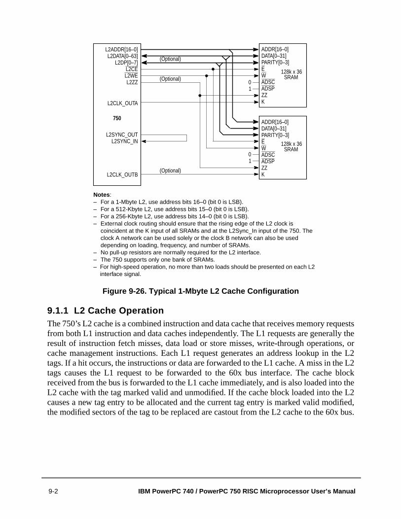
questslly thens, orthe L2e L2block
to thee L2dified,x bus.
Figure 9-26. Typical 1-Mbyte L2 Cache Configuration
9.1.1 L2 Cache OperationThe 750’s L2 cache is a combined instruction and data cache that receives memory refrom both L1 instruction and data caches independently. The L1 requests are generaresult of instruction fetch misses, data load or store misses, write-through operatiocache management instructions. Each L1 request generates an address lookup intags. If a hit occurs, the instructions or data are forwarded to the L1 cache. A miss in thtags causes the L1 request to be forwarded to the 60x bus interface. The cachereceived from the bus is forwarded to the L1 cache immediately, and is also loaded inL2 cache with the tag marked valid and unmodified. If the cache block loaded into thcauses a new tag entry to be allocated and the current tag entry is marked valid mothe modified sectors of the tag to be replaced are castout from the L2 cache to the 60
L2ADDR[16–0]L2DATA[0–63]
L2DP[0–7]L2CEL2WEL2ZZ
L2CLK_OUTA
L2SYNC_OUTL2SYNC_IN
L2CLK_OUTB
ADDR[16–0]DATA[0–31]PARITY[0–3]EWADSCADSPZZK
750ADDR[16–0]DATA[0–31]PARITY[0–3]EWADSCADSPZZK
10
01
(Optional)
(Optional)
Notes :– For a 1-Mbyte L2, use address bits 16–0 (bit 0 is LSB).– For a 512-Kbyte L2, use address bits 15–0 (bit 0 is LSB).– For a 256-Kbyte L2, use address bits 14–0 (bit 0 is LSB).– External clock routing should ensure that the rising edge of the L2 clock is
coincident at the K input of all SRAMs and at the L2Sync_In input of the 750. Theclock A network can be used solely or the clock B network can also be useddepending on loading, frequency, and number of SRAMs.
– No pull-up resistors are normally required for the L2 interface.– The 750 supports only one bank of SRAMs.– For high-speed operation, no more than two loads should be presented on each L2
interface signal.
(Optional)
128k x 36SRAM
128k x 36SRAM
9-2 IBM PowerPC 740 / PowerPC 750 RISC Microprocessor User’s Manual

d the2 cacheests toquestsity in
he canctionnder-ulting
che isre incacheriteshe L2g burst50 for
d thebe
to be
se anysingle-cachele-beatquestsn ofusthee thatfault
hange.
At any given time the L1 instruction cache may have one instruction fetch request, anL1 data cache may have one load and two stores requesting L2 cache access. The Lalso services snoop requests from the 60x bus. When there are multiple pending requthe L2 cache, snoop requests have highest priority, followed by data load and store re(serviced on a first-in, first-out basis). Instruction fetch requests have the lowest prioraccessing the L2 cache when there are multiple accesses pending.
If read requests from both the L1 instruction and data caches are pending, the L2 cacperform hit-under-miss and supplies the available instruction or data while a bus transafor the previous L2 cache miss is performed. The L2 cache does not support miss-umiss, and the second instruction fetch or data load stalls until the bus operation resfrom the first L2 miss completes.
All requests to the L2 cache that are marked cacheable (even if the respective L1 cadisabled or locked) cause tag lookup and will be serviced if the instructions or data athe L2 cache. Burst and single-beat read requests from the L1 caches that hit in the L2are forwarded instructions or data, and the L2 LRU bit for that tag is updated. Burst wfrom the L1 data cache due to a castout or replacement copyback are written only to tcache, and the L2 cache sector is marked modified. Designers should note that durintransfers into and out of the L2 cache SRAM array, an address is generated by the 7each data beat.
If the L2 cache is configured as write-through, the L2 sector is marked unmodified, anwrite is forwarded to the 60x bus. If the L1 castout requires a new L2 tag entry toallocated and the current tag is marked modified, any modified sectors of the tagreplaced are cast out of the L2 cache to the 60x bus.
Single-beat read requests from the L1 caches that miss in the L2 cache do not caustate changes in the L2 cache and are forwarded on the 60x bus interface. Cacheablebeat store requests marked copy-back that hit in the L2 are allowed to update the L2sector, but do not cause L2 cache sector allocation or deallocation. Cacheable, singstore requests that miss in the L2 are forwarded to the 60x bus. Single-beat store remarked write-through (through address translation or through the configuratioL2CR[L2WT]) are written to the L2 cache if they hit and are written to the 60x bindependent of the L2 hit/miss status. If the store hits in the L2 cache,modified/unmodified status of the tag remains unchanged. All requests to the L2 cachare marked cache-inhibited by address translation (through either the MMU or by deWIMG configuration) bypass the L2 cache and do not cause any L2 cache tag state c
Chapter 9. L2 Cache Interface Operation 9-3

he.L1 andd with, theIf theions
gh
inor
TheL1
m ther-only
uiresmuste L2
2 byteive) ofmust
ationst ifer
hitsletes.for
che
s.
The execution of thestwcx. instruction results in single-beat writes from the L1 data cacThese single-beat writes are processed by the L2 cache according to hit/miss status,L2 write-through configuration, and reservation-active status. If the address associatethestwcx. instruction misses in the L2 cache or if the reservation is no longer activestwcx. instruction bypasses the L2 cache and is forwarded to the 60x bus interface.stwcx. hits in the L2 cache and the reservation is still active, one of the following actoccurs:
• If the stwcx. hits a modified sector in the L2 cache (independent of write-throustatus), or if thestwcx.hits both the L1 and L2 caches in copy-back mode, thestwcx.is written to the L2 and the reservation completes.
• If the stwcx.hits an unmodified sector in the L2 cache, and either the L1 or L2 iswrite-through mode, thestwcx. is forwarded to the 60x bus interface and the secthit in the L2 cache is invalidated.
L1 cache-block-push operations generated by the execution ofdcbf anddcbst instructionswrite through to the 60x bus interface and invalidate the L2 cache sector if they hit.execution ofdcbf anddcbst instructions that do not cause a cache-block-push from thecache are forwarded to the L2 cache to perform a sector invalidation and/or push froL2 cache to the 60x bus as required. If thedcbf anddcbst instructions do not cause a sectopush from the L2 cache, they are forwarded to the 60x bus interface for addressbroadcast if HID0[ABE] is set to 1.
The L2 flush mechanism is similar to the L1 data cache flush mechanism. L2 flush reqthat the entire L1 data cache be flushed prior to flushing the L2 cache. Also, interruptsbe disabled during the L2 flush so that the LRU algorithm does not get disturbed. Thcan be flushed by executing uniquely addressed load instructions to each of the 3blocks of the L2 cache. This requires a load to each of the 2 sets (2-way set associatthe 32-byte block (sector) within each 64 or 128-byte line of the L2 cache. The loadsnot hit in the L1 cache in order to effect a flush of the L2 cache.
Thedcbi instruction is always forwarded to the L2 cache and causes a segment invalidif a hit occurs. The instruction is also forwarded to the 60x bus interface for broadcaHID0[ABE] is set to 1. Theicbi instruction invalidates only L1 cache blocks and is nevforwarded to the L2 cache.
Any dcbz instructions marked global do not affect the L2 cache state. If an instructionin the L1 and L2 caches, the L1 data cache block is cleared and the instruction compIf an instruction misses in the L2 cache, it is forwarded to the 60x bus interfacebroadcast. Anydcbz instructions that are marked nonglobal act only on the L1 data cawithout reference to the state of the L2.
Thesync andeieio instructions bypass the L2 cache and are forwarded to the 60x bu
9-4 IBM PowerPC 740 / PowerPC 750 RISC Microprocessor User’s Manual

R is a1017.L2CR.1.5,
9.1.2 L2 Cache Control Register (L2CR)The L2 cache control register is used to configure and enable the L2 cache. The L2Csupervisor-level read/write, implementation-specific register that is accessed as SPRThe contents of the L2CR are cleared during power-on reset. Table 9-8 describes thebits. For additional information about the configuration of the L2CR, refer to Section 2“L2 Cache Control Register (L2CR).”
Table 9-8. L2 Cache Control Register
Bit Name Function
0 L2E L2 enable
1 L2PE L2 data parity generation and checking enable
2–3 L2SIZ L2 size—Should be set according to the size of the L2 data RAMs used00 Reserved01 256 Kbyte10 512 Kbyte11 1 Mbyte
4–6 L2CLK L2 clock ratio (core-to-L2 frequency divider)000 L2 clock and DLL disabled001 ÷1010 ÷1.5011 Reserved100 ÷2101 ÷2.5110 ÷3111 Reserved
7–8 L2RAM L2 RAM type—Configures the L2 RAM interface for the type of synchronous SRAMs used00 Flow-through (register-buffer) synchronous burst SRAM01 Reserved10 Pipelined (register-register) synchronous burst SRAM11 Pipelined (register-register) synchronous late-write SRAM
9 L2DO L2 data-only. Setting this bit disables the caching of instructions in the L2 cache.
10 L2I L2 global invalidate. Setting L2I invalidates the L2 cache globally by clearing the L2 statusbits.
11 L2CTL L2 RAM control (ZZ enable). Setting L2CTL enables the automatic operation of the L2ZZ(low-power mode) signal for cache RAMs that support the ZZ function. This bit should notbe set when the 750 is in nap mode and snooping is being performed through deassertionof QACK.
12 L2WT L2 write-through. Setting L2WT selects write-through mode (rather than the default copy-back mode) so all writes to the L2 cache also write through to the 60x bus.
13 L2TS L2 test support. Setting L2TS causes cache block pushes from the L1 data cache thatresult from dcbf and dcbst instructions to be written only into the L2 cache and markedvalid, rather than being written only to the 60x bus and marked invalid in the L2 cache incase of hit. If L2TS is set, causes single-beat store operations that miss in the L2 cache tobe discarded.
Chapter 9. L2 Cache Interface Operation 9-5

ally.CR
eforethe L2start-
rouldnd
bal
9.1.3 L2 Cache InitializationFollowing a power-on or hard reset, the L2 cache and the L2 DLL are disabled initiBefore enabling the L2 cache, the L2 DLL must first be configured through the L2register, and the DLL must be allowed 640 L2 clock periods to achieve phase lock. Benabling the L2 cache, other configuration parameters must be set in the L2CR, andtags must be globally invalidated. The L2 cache should be initialized during systemup.
The sequence for initializing the L2 cache is as follows:
1. Power-on reset (automatically performed by the assertion ofHRESET signal).
2. Disable interrupts and Dynamic Power Management (DPM).
3. Disable L2 cache by clearing L2 CR[L2E].
4. Set the L2CR[L2CLK] bits to the desired clock divider setting. Setting a nonzevalue automatically enables the DLL. All other L2 cache configuration bits shobe set to properly configure the L2 cache interface for the SRAM type, size, ainterface timing required.
5. Wait for the L2 DLL to achieve phase lock. This can be timed by setting thedecrementer for a time period equal to 640 L2 clocks, or by performing an L2 gloinvalidate.
14–15 L2OH L2 output hold. These bits configure the output hold time of the address, data, and controlsignals driven by the 750 to the L2 data RAMs.00 0.5 nS01 1.0 nS10 Reserved11 Reserved
16 L2SL L2 DLL slow. Setting L2SL enables L2 data RAM clocking at frequencies less than100 MHz.
17 L2DF L2 differential clock. Setting L2DF configures the two clock-out signals (L2CLK_OUTA andL2CLK_OUTB) of the L2 interface to operate as one differential clock.
18 L2BYP L2 DLL bypass. L2BYP is intended for use when the PLL is being bypassed, and forengineering evaluation.
19–21 — Reserved. These bits are implemented but not used; keep at 0 for future compatibility.
22 L2CS L2 Clock Stop (for chip revisions 3.0 and later).
23 L2DRO L2 DLL Rollover Checkstop Enable (for chip revisions 3.0 and later).
24-30 L2CTR L2 DLL counter value (read only).
31 L2IP L2 global invalidate in progress (read only)—This read-only bit indicates whether an L2global invalidate is occurring.
Table 9-8. L2 Cache Control Register (Continued)
Bit Name Function
9-6 IBM PowerPC 740 / PowerPC 750 RISC Microprocessor User’s Manual

ore
hen it
ther by
(tagwarectionis
e L2
re
n the
is
L2
ion oftionsddressarded
ntsaintentsload
6. Perform an L2 global invalidate. The global invalidate could be performed befenabling the DLL, or in parallel with waiting for the DLL to stabilize. Refer toSection 9.1.4, “L2 Cache Global Invalidation,” for more information about L2 cacglobal invalidation. Note that a global invalidate always takes much longer thatakes for the DLL to stabilize.
7. After the DLL stabilizes, an L2 global invalidate has been performed, and the oL2 configuration bits have been set, enable the L2 cache for normal operationsetting the L2CR[L2E] bit to 1.
9.1.4 L2 Cache Global InvalidationThe L2 cache supports a global invalidation function in which all bits of the L2 tagsdata bits, tag status bits, and LRU bit) are cleared. It is performed by an on-chip hardstate machine that sequentially cycles through the L2 tags. The global invalidation funis controlled through L2CR[L2I], and it must be performed only while the L2 cachedisabled. The 750 can continue operation during a global invalidation provided thcache has been properly disabled before the global invalidation operation starts.
The sequence for performing a global invalidation of the L2 cache is as follows:
1. Execute async instruction to finish any pending store operations in the load/stounit, disable the L2 cache by clearing L2CR[L2E], and execute an additionalsyncinstruction after disabling the L2 cache to ensure that any pending operations iL2 cache unit have completed.
2. Initiate the global invalidation operation by setting the L2CR[L2I] bit to 1.
3. Monitor the L2CR[L2IP] bit to determine when the global invalidation operationcompleted (indicated by the clearing of L2CR[L2IP]). The global invalidationrequires approximately 32K core clock cycles to complete.
4. After detecting the clearing of L2CR[L2IP], clear L2CR[L2I] and re-enable thecache for normal operation by setting L2CR[L2E].
9.1.5 L2 Cache Test Features and MethodsIn the course of system power-up, testing may be required to verify the proper operatthe L2 tag memory, external SRAM, and overall L2 cache system. The following secdescribe the 750’s features and methods for testing the L2 cache. The L2 cache aspace should be marked as guarded (G = 1) so spurious load operations are not forwto the 60x bus interface before branch resolution during L2 cache testing.
9.1.5.1 L2CR Support for L2 Cache TestingL2CR[DO] and L2CR[TS] support the testing of the L2 cache. L2CR[DO] preveinstructions from being cached in the L2. This allows the L1 instruction cache to remenabled during the testing process without having L1 instruction misses affect the conof the L2 cache and allows all L2 cache activity to be controlled by program-specifiedand store operations.
Chapter 9. L2 Cache Interface Operation 9-7

e.ing aache.
ck.
o hit inhe L2ddresshenage tablee hass then
eablemiss.
ts androper
rnal
fault
can
ng adthe L2executeterns
ts or
nownof stores
ssesbusan be
L2CR[TS] is used with thedcbf anddcbst instructions to push data into the L2 cachWhen L2CR[TS] is set, and the L1 data cache is enabled, an instruction loop containdcbf instruction can be used to store any address or data pattern to the L2 cAdditionally, 60x bus broadcasting is inhibited when adcbz instruction is executed. Thisallows the use of adcbz instruction to clear an L1 cache block, followed by adcbfinstruction to push the cache block into the L2 cache and invalidate the L1 cache blo
When the L2 cache is enabled, cacheable single-beat read operations are allowed tthe L2 cache and cacheable write operations are allowed to modify the contents of tcache when a hit occurs. Cacheable single-beat read and writes occur when atranslation is disabled (invoking the use of the default WIMG bits (0b0011)), or waddress translation is enabled and accesses are marked as cacheable through the pentries or the BATs, and the L1 data cache is disabled or locked. When the L2 cachbeen initialized and the L1 cache has been disabled or locked, load or store instructionbypass the L1 cache and hit in the L2 cache directly. When L2CR[TS] is set, cachsingle-beat writes are inhibited from accessing the 60x bus interface after an L2 cache
During L2 cache testing, the performance monitor can be used to count L2 cache himisses, thereby providing a numerical signature for test routines and a way to verify pL2 cache operation.
9.1.5.2 L2 Cache TestingA typical test for verifying the proper operation of the 750’s L2 cache memory (exteSRAM and tag) would perform the following steps:
1. Initialize the L2 test sequence by disabling address translation to invoke the deWIMG setting (0b0011). Set L2CR[DO] and L2CR[TS] and perform a globalinvalidation of the L1 data cache and the L2 cache. The L1 instruction cache remain enabled to improve execution efficiency.
2. Test the L2 cache external SRAM by enabling the L1 data cache and executisequence ofdcbz, stw, anddcbf instructions to initialize the L2 cache with a desirerange of consecutive addresses and with cache data consisting of zeros. Oncecache holds a sequential range of addresses, disable the L1 data cache and a series of single-beat load and store operations employing a variety of bit patto test for stuck bits and pattern sensitivities in the L2 cache SRAM. Theperformance monitor can be used to verify whether the number of L2 cache himisses corresponds to the tests performed.
3. Test the L2 cache tag memory by enabling the L1 data cache and executing asequence ofdcbz, stw, anddcbf instructions to initialize the L2 cache with a widerange of addresses and cache data. Once the L2 cache is populated with a krange of addresses and data, disable the L1 data cache and execute a seriesoperations to addresses not previously in the L2 cache. These store operationshould miss in every case. Note that setting the L2CR[TS] inhibits L2 cache mifrom being forwarded to the 60x bus interface, thereby avoiding the potential forerrors due to addressing hardware or nonexistent memory. The L2 cache then c
9-8 IBM PowerPC 740 / PowerPC 750 RISC Microprocessor User’s Manual

etheranceand
ring
gramn be
. Theby
k isrface
L).
ternaltmentnal
urstcheingselectnersy, an
steme the-offs
dataugh, butbus
nd 3.
further verified by reading the previously loaded addresses and observing whall the tags hit, and that the associated data compares correctly. The performmonitor can also be used to verify whether the proper number of L2 cache hitsmisses correspond to the test operations performed.
4. The entire L2 cache can be tested by clearing L2CR[DO] and L2CR[TS], restothe L1 and L2 caches to their normal operational state, and executing acomprehensive test program designed to exercise all the caches. The test proshould include operations that cause L2 hit, reload, and castout activity that casubsequently verified through the performance monitor.
9.1.6 L2 Clock ConfigurationThe 750 provides a programmable clock for the L2 external synchronous data RAMclock frequency for the external SRAM is provided by dividing the 750’s internal clockratios of 1, 1.5, 2, 2.5, or 3, programmed through the L2CR[CLK] bits. The L2 clocphase-adjusted to synchronize the clocking of the latches in the 750’s L2 cache intewith the clocking of the external SRAM by means of an on-chip delay-locked loop (DL
The ratio selected for the L2 clock is dependent on the frequency supported by the exSRAMs, the 750’s internal frequency of operation, and the range of phase adjussupported by the L2 DLL. Refer to the 750 hardware specifications for additioinformation about L2 clock configuration.
9.1.7 L2 Cache SRAM Timing ExamplesThis section describes the signal timing for the three types of SRAM (flow-through bSRAM, pipelined burst SRAM, and late-write SRAM) supported by the 750’s L2 cainterface. The timing diagrams illustrate the best case logical (ideal, non AC-timaccurate) interface operations. For proper interface operation, the designer mustSRAMs that support the signal sequencing illustrated in the timing diagrams. Desigshould also note that during burst transfers into and out of the L2 cache SRAM arraaddress is generated by the 750 for each data beat.
The SRAM selected for a system design is usually a function of desired syperformance, L2 bus frequency, and SRAM unit cost. The following sections describoperation of the three SRAM types supported by the 750, and the design tradeassociated with each.
9.1.7.1 Flow-Through Burst SRAMFlow-through burst SRAMs operate by clocking in the address, and driving thedirectly to the bus from the SRAM memory array. This behavior allows the flow-throburst SRAMs to provide initial read data one cycle sooner than pipelined burst SRAMsthe flow-through burst SRAM frequencies available may only support the slowest L2frequencies. The 750 supports flow-through burst SRAM at L2 clock ratios of 2, 2.5,a
Chapter 9. L2 Cache Interface Operation 9-9

cache
cache
Figure 9-27 shows a burst read-write-read memory access sequence when the L2interface is configured with flow-through burst SRAM.
Figure 9-27. Burst Read-Write-Read L2 Cache Access (Flow-Through)
Figure 9-28 shows a burst read-modify-write memory access sequence when the L2interface is configured with flow-through burst SRAM.
Figure 9-28. Burst Read-Modify-Write L2 Cache Access (Flow-Through)
burst wrburst rd burst rd
Note : Rxtr indicates where an extra read cycle is signaled to keep the burst RAM driving the
data bus for the last read.
hiZ hiZ
R0 R1 R2 R3 Rxtr W4 W5 W6 W7 R8 R9 R10 R11 Rxtr
R0 R1 R2 R3 Rxtr W4 W5 W6 W7 R8 R9 R10 R11 Rxtr
R0 R1 R2 R3 Rxtr W4 W5 W6 W7 R8 R9 R10 R11 Rxtr
SRAMClk
L2CE
L2WE
SRAMAddress
SRAMMemory
SRAMData
rd modify wr
Note : Rxtr indicates where an extra read cycle is signaled to keep the burst RAM driving the
data bus for the last read.
hiZ
burst wrburst rdburst rd
R0 R1 R2 R3 W9 W10 W11 W12 W13RxtrR4 R5 R6 R7 R8
R0 R1 R2 R3 W9 W10 W11 W12 W13RxtrR4 R5 R6 R7 R8
R0 R1 R2 R3 W9 W10 W11 W12 W13RxtrR4 R5 R6 R7 R8
SRAMData
L2WE
L2CE
SRAMClk
SRAMAddress
SRAMMemory
9-10 IBM PowerPC 740 / PowerPC 750 RISC Microprocessor User’s Manual

cache
s byo thee cycleigher.elined
cache
Figure 9-29 shows a burst read-write-write memory access sequence when the L2interface is configured with flow-through burst SRAM.
Figure 9-29. Burst Read-Write-Write L2 Cache Access (Flow-Through)
9.1.7.2 Pipelined Burst SRAMPipelined burst SRAMs operate at higher frequencies than flow-through burst SRAMclocking the read data from the memory array into a buffer before driving the data ontdata bus. This causes initial read accesses by the pipelined burst SRAMs to occur onlater than flow-through burst SRAMs, but the L2 bus frequencies supported can be hNote that the 750’s L2 cache interface requires the use of single-cycle deselect pipburst SRAM for proper operation.
Figure 9-30 shows a burst read-write-read memory access sequence when the L2interface is configured with pipelined burst SRAM.
Figure 9-30. Burst Read-Write-Read L2 Cache Access (Pipelined)
Note : Rxtr indicates where an extra read cycle is signaled to keep the burst RAM driving the
data bus for the last read.
burst wrburst rd burst wraborted rdR0 R1 R2 R3 W8 W9 W10 W11 W12R4 W7W6Rxtr W5
R0 R1 R2 R3 W8 W9 W10 W11 W12R4 W7W6Rxtr W5
R0 R1 R2 R3 W8 W9 W10 W11 W12R4 W7W6Rxtr W5hiZhiZSRAMData
L2WE
L2CE
SRAMClk
SRAMAddress
SRAMMemory
burst wrburst rd burst rd
Notes : Rdrv indicates where some burst RAMs may begin driving the data bus. Rxtr indicates where an extra read cycle is signaled to keep the burst RAM driving the
data bus for the last read.
R0 R1 R2 R3 Rxtr W4 W5 W6 W7 R8 R9 R10 R11 Rxtr
R0 R1 R2 R3 Rxtr W4 W5 W6 W7 R8 R9 R10 R11 Rxtr
R0 R1 R2 W4 W5 W6 W7 RdrvRdrv R3 R8 R9 R10 R11hiZ hiZSRAMData
L2WE
L2CE
SRAMClk
SRAMAddress
SRAMMemory
Chapter 9. L2 Cache Interface Operation 9-11

cache
cache
AMslessantionon the
en read
Figure 9-31 shows a burst read-modify-write memory access sequence when the L2interface is configured with pipelined burst SRAM.
Figure 9-31. Burst Read-Modify-Write L2 Cache Access (Pipelined)
Figure 9-32 shows a burst read-write-write memory access sequence when the L2interface is configured with pipelined burst SRAM.
Figure 9-32. Burst Read-Write-Write L2 Cache Access (Pipelined)
9.1.7.3 Late-Write SRAMLate-write SRAMs offer improved performance when compared to pipelined burst SRby not requiring an extra read cycle during read operations, and requiring one cyclewhen transitioning from a read to write operation. Late-write SRAMs implementinternal write queue, allowing write data to be provided one cycle after the write operais signaled on the address and control buses. In this way write operations are queuedaddress and data bus in the same way as read operations, allowing transitions betweand write operations to occur more efficiently.
rd modify wr
Notes : Rdrv indicates where some burst RAMs may begin driving the data bus. Rxtr indicates where an extra read cycle is signaled to keep the burst RAM driving the
data bus for the last read.
burst wrburst rdburst rd
R0 R1 R2 R3 W9 W10 W11 W12 W13RxtrR4 R5 R6 R7 R8
W9 W10 W11 W12 W13Rdrv
R0 R1 R2 R3 W9 W10 W11 W12 W13RxtrR4 R5 R6 R7 R8
R0 R1 R2 R3 R4 R5 R6 R7 R8 hiZSRAMData
L2WE
L2CE
SRAMClk
SRAMAddress
SRAMMemory
Notes : Rdrv indicates where some burst RAMs may begin driving the data bus. Rxtr indicates where an extra read cycle is signaled to keep the burst RAM driving the
data bus for the last read.
burst wrburst rd burst wraborted rdR0 R1 R2 R3 W8 W9 W10 W11 W12R4 W7W6Rxtr W5
R0 R1 R2 R3 W8 W9 W10 W11 W12R4 W7W6Rxtr W5
W8 W9 W10 W11 W12W7W6Rdrv W5R1 R2 R3 R4Rdrv hiZhiZSRAMData
L2WE
L2CE
SRAMClk
SRAMAddress
SRAMMemory
9-12 IBM PowerPC 740 / PowerPC 750 RISC Microprocessor User’s Manual

cache
cache
Figure 9-33 shows a burst read-write-read memory access sequence when the L2interface is configured with late-write SRAM.
Figure 9-33. Burst Read-Write-Read L2 Cache Access (Late-Write SRAM)
Figure 9-34 shows a burst read-modify-write memory access sequence when the L2interface is configured with late-write SRAM.
Figure 9-34. Burst Read-Modify-Write L2 Cache Access (Late-Write SRAM)
burst wrburst rd burst rd
Note : WQ is the last previous write that was queued in the late-write RAM.
R0 R1 R2 R3 W4 W5 W6 W7 R8 R9 R10 R11
R0 R1 R2 R3 (WQ) W4 W5 W6 R8 R9 R10 R11
R0 R1 R2 W4 W5 W6 W7R3 R8 R9 R10 R11hiZhiZSRAMData
L2WE
L2CE
SRAMClk
SRAMAddress
SRAMMemory
rd modify wr burst wrburst rdburst rd
Note : WQ is the last previous write that was queued in the late-write RAM.
R0 R1 R2 R3 R4 R5 R6 R7 R8
W9 W10 W11 W12 W13
R0 R1 R2 R3 W9 W10 W11 W12 W13R4 R5 R6 R7 R8
R0 R1 R2 R3 R4 R5 R6 R7 R8
W9 W10 W11 W12(WQ)
hiZSRAMData
L2WE
L2CE
SRAMClk
SRAMAddress
SRAMMemory
Chapter 9. L2 Cache Interface Operation 9-13

cache
Figure 9-35 shows a burst read-write-write memory access sequence when the L2interface is configured with late-write SRAM.Figure 9-35. Burst Read-Write-Write L2 Cache Access (Late-Write SRAM)
Note : WQ is the last previous write that was queued in the late-write RAM.
burst wrburst rd burst wraborted rdR0 R1 R2 R3 W8 W9 W10 W11 W12R4 W7W6W5
R0 R1 R2 R3 W8 W9 W10 W11R4 W7W6W5
W8 W9 W10 W11 W12W7W6W5R1 R2 R3 R4R0
(WQ)
hiZhiZ
W12
SRAMData
L2WE
L2CE
SRAMClk
SRAMAddress
SRAMMemory
9-14 IBM PowerPC 740 / PowerPC 750 RISC Microprocessor User’s Manual

n. Itssiveon-
high-by the
dualmple,allyeachon a
notwerernal
leep.modeternal
flow to750
ystementerowerpower
odeerencypower
Chapter 10Power and Thermal Management100100
The PowerPC 750 microprocessor is specifically designed for low-power operatioprovides both automatic and program-controlled power reduction modes for progrereduction of power consumption. It also provides a thermal assist unit (TAU) to allowchip thermal measurement, allowing sophisticated thermal management forperformance portable systems. This chapter describes the hardware support provided750 for power and thermal management.
10.1 Dynamic Power ManagementDynamic power management (DPM) automatically powers up and down the indiviexecution units of the 750, based upon the contents of the instruction stream. For exaif no floating-point instructions are being executed, the floating-point unit is automaticpowered down. Power is not actually removed from the execution unit; instead,execution unit has an independent clock input, which is automatically controlledclock-by-clock basis. Since CMOS circuits consume negligible power when they areswitching, stopping the clock to an execution unit effectively eliminates its poconsumption. The operation of DPM is completely transparent to software or any exthardware. Dynamic power management is enabled by setting HID0[DPM] to 1.
10.2 Programmable Power ModesThe 750 provides four programmable power states—full power, doze, nap, and sSoftware selects these modes by setting one (and only one) of the three power savingbits in the HID0 register. Hardware can enable a power management state through exasynchronous interrupts. Such a hardware interrupt causes the transfer of programinterrupt handler code that then invokes the appropriate power saving mode. Theprovides a separate interrupt and interrupt vector for power management—the smanagement interrupt (SMI). The 750 also contains a decrementer which allows it tothe nap or doze mode for a predetermined amount of time and then return to full poperation through a decrementer interrupt. Note that the 750 cannot switch from onemanagement mode to another without first returning to full-power mode. The sleep mdisables bus snooping; therefore, a hardware handshake is provided to ensure cohbefore the 750 enters this power management mode. Table 10-1 summarizes the fourstates.
Chapter 10. Power and Thermal Management 10-1

odes,bilities
ID0
er
ng thee, copy
10.2.1 Power Management ModesThe following sections describe the characteristics of the 750’s power management mthe requirements for entering and exiting the various modes, and the system capaprovided by the 750 while the power management modes are active.
10.2.1.1 Full-Power Mode with DPM DisabledFull-power mode with DPM disabled is selected when the DPM enable bit (bit 11) in His cleared.
• Default state following power-up andHRESET• All functional units are operating at full processor speed at all times.
10.2.1.2 Full-Power Mode with DPM EnabledFull-power mode with DPM enabled (HID0[DPM] = 1) provides on-chip powmanagement without affecting the functionality or performance of the 750.
• Required functional units are operating at full processor speed.• Functional units are clocked only when needed.• No software or hardware intervention is required after mode is set.• Software/hardware and performance transparent
10.2.1.3 Doze ModeDoze mode disables most functional units but maintains cache coherency by enablibus interface unit and snooping. A snoop hit causes the 750 to enable the data cachthe data back to memory, disable the cache, and fully return to the doze state.
Table 10-1. PowerPC 750 Microprocessor Programmable Power Modes
PM Mode Functioning Units Activation Method Full-Power Wake Up Method
Full power All units active — —
Full power(with DPM)
Requested logic bydemand
By instruction dispatch —
Doze • Bus snooping• Data cache as needed• Decrementer timer
Controlled by SW External asynchronous exceptions*Decrementer interruptPerformance monitor interruptThermal management interruptHard or soft reset
Nap • Bus snooping— enabled by deassertion
of QACK• Decrementer timer
Controlled by hardwareand software
External asynchronous exceptions*Decrementer interruptHard or soft reset
Sleep None Controlled by hardwareand software
External asynchronous exceptions*Hard or soft reset
Note : * Exceptions are referred to as interrupts in the architecture specification.
10-2 IBM PowerPC 740 / PowerPC 750 RISC Microprocessor User’s Manual

0)
or
delaye/fter ar naprequest
oopinget
cycle.ity.e
es tothishasllowsy time.
ry toZwerng then of
• Most functional units disabled• Bus snooping and time base/decrementer still enabled• Doze mode sequence
— Set doze bit (HID0[8] = 1), clear nap and sleep bits (HID0[9] and HID0[10] =— The 750 enters doze mode after several processor clocks
• Several methods of returning to full-power mode
— AssertINT, SMI, MCP, decrementer, performance monitor, machine check,thermal management interrupts
— Assert hard reset or soft reset
• Transition to full-power state takes no more than a few processor cycles• PLL running and locked to SYSCLK
10.2.1.4 Nap ModeThe nap mode disables the 750 but still maintains the phase-locked loop (PLL),locked loop (DLL), L2CLK_OUTA and L2CLK_OUTB output signals, and the time basdecrementer. The time base can be used to restore the 750 to full-power state aprogrammed amount of time. To maintain data coherency, bus snooping is disabled foand sleep modes through a hardware handshake sequence using the quiesce(QREQ) and quiesce acknowledge (QACK) signals. The 750 asserts theQREQ signal toindicate that it is ready to disable bus snooping. When the system has ensured that snis no longer necessary, it will assertQACK and the 750 will enter the nap mode. If thsystem determines that a bus snoop cycle is required,QACK is deasserted to the 750 for aleast eight bus clock cycles, and the 750 will then be able respond to a snoopAssertion ofQACK following the snoop cycle will again disable the 750’s snoop capabilThe 750’s power dissipation while in nap mode withQACK deasserted is the same as thpower dissipation while in doze mode.
The 750 (2.0 and later) also allows dynamic switching between nap and doze modallow the use of nap mode without sacrificing hardware snoop coherency. Foroperation, negatingQACK at any time for at least 8 bus cycles guarantees that the 750transitioned from nap mode to doze mode in order to snoop. Reasserting QACK then athe 750 to return to nap mode. This sequencing could be used by the system at anwith knowledge of what power management mode, if any, that the 750 is currently in
Note that when in nap mode the DLL should be kept locked to enable a quick recovefull-power mode without having to wait for the DLL to re-lock. Additionally, an L2Zsignal is provided by the 750’s L2 cache interface to drive external SRAM into a low pomode when the nap or sleep modes are invoked. The L2ZZ signal is enabled by settiL2CR[CTL] bit to 1. Note that if bus snooping is to be performed through deassertiotheQACK signal, the L2CR[CTL] bit should always be cleared to 0.
• Time base/decrementer still enabled
• Thermal management unit enabled
Chapter 10. Power and Thermal Management 10-3

0)
l unitsd bythatwillmode.ndy
n nothe 750l time
eforeoessary,
• Most functional units disabled
• All nonessential input receivers disabled
• Nap mode sequence
— Set nap bit (HID0[9] = 1), clear doze and sleep bits (HID0[8] and HID0[10] =
— The 750 asserts quiesce request (QREQ) signal
— System asserts quiesce acknowledge (QACK) signal
— The 750 enters sleep mode after several processor clocks
• Nap mode bus snoop sequence
— System deassertsQACK signal for eight or more bus clock cycles
— The 750 snoops address tenure(s) on bus
— System assertsQACK signal to restore full nap mode
• Several methods of returning to full-power mode
— AssertINT, SMI, MCP, machine check, or decrementer interrupts— Assert hard reset or soft reset
• Transition to full-power takes no more than a few processor cycles• PLL and DLL running and locked to SYSCLK.
10.2.1.5 Sleep ModeSleep mode consumes the least amount of power of the four modes since all functionaare disabled. To conserve the maximum amount of power, the PLL may be disableplacing the PLL_CFG signals in the PLL bypass mode, and disabling SYSCLK. Noteforcing the SYSCLK signal into a static state does not disable the 750’s PLL, whichcontinue to operate internally at an undefined frequency unless placed in PLL bypassAdditionally, if the PLL is not disabled, the L2 cache interface DLL will remain locked athe L2CLK_OUTA and L2CLK_OUTB signals will remain active. The DLL is disabled bclearing the L2CR[L2E] bit to 0.
Due to the fully static design of the 750, internal processor state is preserved wheinternal clock is present. Because the time base and decrementer are disabled whileis in sleep mode, the 750’s time base contents will have to be updated from an externabase after exiting sleep mode if maintaining an accurate time-of-day is required. Bentering the sleep mode, the 750 asserts theQREQ signal to indicate that it is ready tdisable bus snooping. When the system has ensured that snooping is no longer necit assertsQACK and the 750 will enter sleep mode.
• All functional units disabled (including bus snooping and time base)• All nonessential input receivers disabled
— Internal clock regenerators disabled— PLL and DLL still running (see below)
10-4 IBM PowerPC 740 / PowerPC 750 RISC Microprocessor User’s Manual

)
ode
SMI)
2
ust bemodesementowerter on,cleanecute
• Sleep mode sequence
— Set sleep bit (HID0[10] = 1), clear doze and nap bits (HID0[8] and HID0[9]— The 750 asserts quiesce request (QREQ)— System asserts quiesce acknowledge (QACK)— The 750 enters sleep mode after several processor clocks
• Several methods of returning to full-power mode
— AssertINT, SMI, orMCP interrupts— Assert hard reset or soft reset
• PLL and DLL may be disabled and SYSCLK may be removed while in sleep m• Return to full-power mode after PLL and SYSCLK are disabled in sleep mode
— Enable SYSCLK— Reconfigure PLL into desired processor clock mode— System logic waits for PLL startup and relock time (100 sec)— System logic asserts one of the sleep recovery signals (for example, INT or
— Reconfigure DLL, wait for DLL relock (640 L2 clock cycles) and re-enable Lcache through the L2CR
10.2.2 Power Management Software ConsiderationsSince the 750 is a dual-issue processor with out-of-order execution capability, care mtaken in how the power management mode is entered. Furthermore, nap and sleeprequire all outstanding bus operations to be completed before these power managmodes are entered. Normally, during system configuration time, one of the pmanagement modes would be selected by setting the appropriate HID0 mode bit. Lathe power management mode is invoked by setting the MSR[POW] bit. To ensure atransition into and out of a power management mode, set the MSR[EE] bit to 1 and exthe following code sequence:
sync
mtmsr[POW = 1]
isync
continue
Chapter 10. Power and Thermal Management 10-5

ratingermaltion ofnctionile theonstantlead toeviate
ctionmable
the
alog10-1
iongementine the
10.3 Thermal Assist UnitWith the increasing power dissipation of high-performance processors and opeconditions that span a wider range of temperatures than desktop systems, thmanagement becomes an essential part of system design to ensure reliable operaportable systems. One key aspect of thermal management is ensuring that the jutemperature of the microprocessor does not exceed the operating specification. Whcase temperature can be measured with an external thermal sensor, the thermal cfrom the junction to the case can be large, and accuracy can be a problem. This maylower overall system performance due to the necessary compensation to allmeasurement deficiencies.
The 750 provides the system designer an efficient means of monitoring juntemperature through the incorporation of an on-chip thermal sensor and programcontrol logic to enable a thermal management implementation tightly coupled toprocessor for improved performance and reliability.
10.3.1 Thermal Assist Unit OverviewThe on-chip thermal assist unit (TAU) is composed of a thermal sensor, a digital-to-anconverter (DAC), a comparator, control logic, and three dedicated SPRs. See Figurefor a block diagram of the TAU.
Figure 10-1. Thermal Assist Unit Block Diagram
The TAU provides thermal control by periodically comparing the 750’s juncttemperature against user-programmed thresholds, and generating a thermal manainterrupt if the threshold values are crossed. The TAU also enables the user to determjunction temperature through a software successive approximation routine.
Thermal Sensor
Thermal SensorControl Logic
DAC
Decoder
Latch
Interrupt Control
THRM1 THRM2
THR
M3
Thermal InterruptRequest(0x1700)
10-6 IBM PowerPC 740 / PowerPC 750 RISC Microprocessor User’s Manual
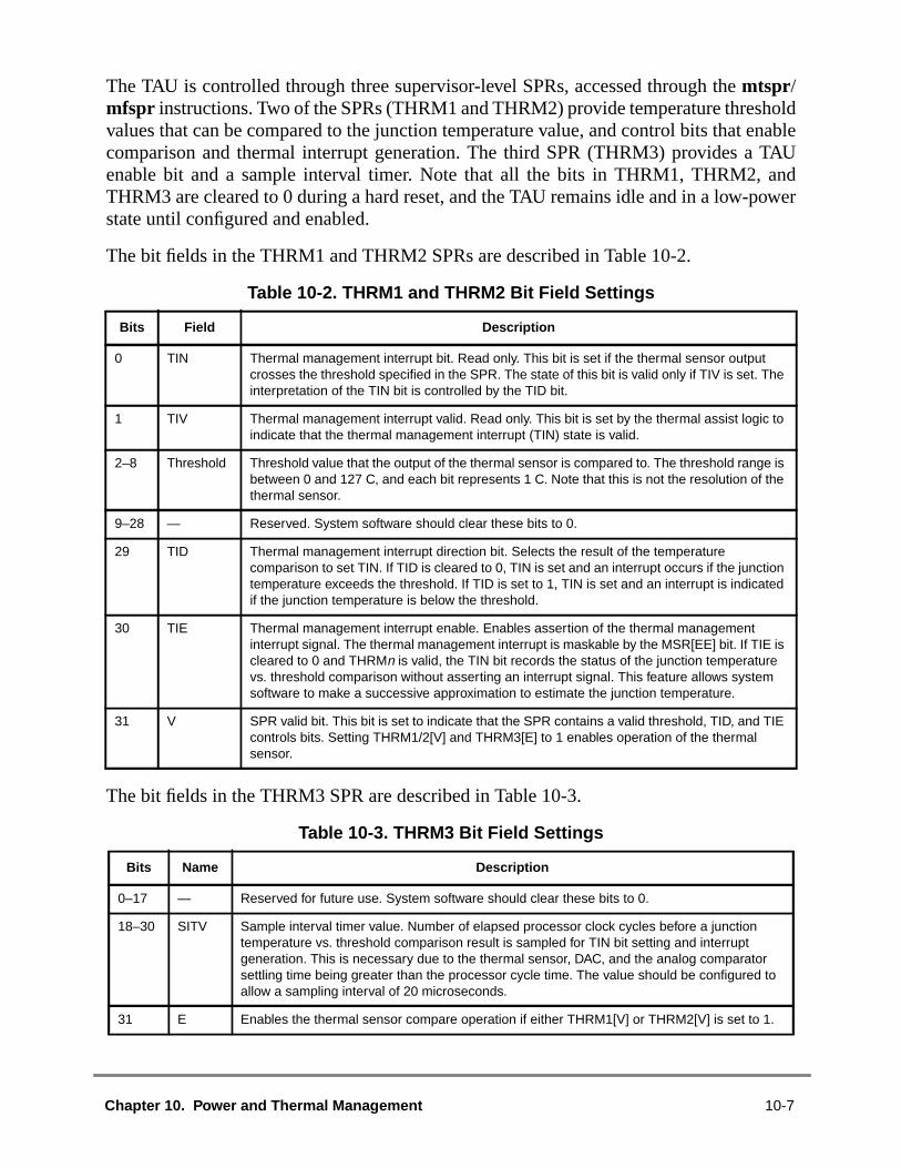
holdenableTAUandower
The TAU is controlled through three supervisor-level SPRs, accessed through themtspr/mfspr instructions. Two of the SPRs (THRM1 and THRM2) provide temperature thresvalues that can be compared to the junction temperature value, and control bits thatcomparison and thermal interrupt generation. The third SPR (THRM3) provides aenable bit and a sample interval timer. Note that all the bits in THRM1, THRM2,THRM3 are cleared to 0 during a hard reset, and the TAU remains idle and in a low-pstate until configured and enabled.
The bit fields in the THRM1 and THRM2 SPRs are described in Table 10-2.
The bit fields in the THRM3 SPR are described in Table 10-3.
Table 10-2. THRM1 and THRM2 Bit Field Settings
Bits Field Description
0 TIN Thermal management interrupt bit. Read only. This bit is set if the thermal sensor outputcrosses the threshold specified in the SPR. The state of this bit is valid only if TIV is set. Theinterpretation of the TIN bit is controlled by the TID bit.
1 TIV Thermal management interrupt valid. Read only. This bit is set by the thermal assist logic toindicate that the thermal management interrupt (TIN) state is valid.
2–8 Threshold Threshold value that the output of the thermal sensor is compared to. The threshold range isbetween 0 and 127 C, and each bit represents 1 C. Note that this is not the resolution of thethermal sensor.
9–28 — Reserved. System software should clear these bits to 0.
29 TID Thermal management interrupt direction bit. Selects the result of the temperaturecomparison to set TIN. If TID is cleared to 0, TIN is set and an interrupt occurs if the junctiontemperature exceeds the threshold. If TID is set to 1, TIN is set and an interrupt is indicatedif the junction temperature is below the threshold.
30 TIE Thermal management interrupt enable. Enables assertion of the thermal managementinterrupt signal. The thermal management interrupt is maskable by the MSR[EE] bit. If TIE iscleared to 0 and THRMn is valid, the TIN bit records the status of the junction temperaturevs. threshold comparison without asserting an interrupt signal. This feature allows systemsoftware to make a successive approximation to estimate the junction temperature.
31 V SPR valid bit. This bit is set to indicate that the SPR contains a valid threshold, TID, and TIEcontrols bits. Setting THRM1/2[V] and THRM3[E] to 1 enables operation of the thermalsensor.
Table 10-3. THRM3 Bit Field Settings
Bits Name Description
0–17 — Reserved for future use. System software should clear these bits to 0.
18–30 SITV Sample interval timer value. Number of elapsed processor clock cycles before a junctiontemperature vs. threshold comparison result is sampled for TIN bit setting and interruptgeneration. This is necessary due to the thermal sensor, DAC, and the analog comparatorsettling time being greater than the processor cycle time. The value should be configured toallow a sampling interval of 20 microseconds.
31 E Enables the thermal sensor compare operation if either THRM1[V] or THRM2[V] is set to 1.
Chapter 10. Power and Thermal Management 10-7

ults ines arectly
on of
bed whenet thehehisto
thes oroftput;can
, thet is
750’sature
rt
10.3.2 Thermal Assist Unit OperationThe TAU can be programmed to operate in single or dual threshold modes, which resthe TAU generating a thermal management interrupt when one or both threshold valucrossed. In addition, with the appropriate software routine, the TAU can also diredetermine the junction temperature. The following sections describe the configuratithe TAU to support these modes of operation.
10.3.2.1 TAU Single Threshold ModeWhen the TAU is configured for single threshold mode, either THRM1 or THRM2 canused to contain the threshold value, and a thermal management interrupt is generatethe threshold value is crossed. To configure the TAU for single threshold operation, sdesired temperature threshold, TID, TIE, and V bits for either THRM1 or THRM2. Tunused THRMn threshold SPR should be disabled by clearing the V bit to 0. In tdiscussion THRMn refers to the THRM threshold SPR (THRM1 or THRM2) selectedcontain the active threshold value.
After setting the desired operational parameters, the TAU is enabled by settingTHRM3[E] bit to 1, and placing a value allowing a sample interval of 20 microsecondgreater in the THRM3[SITV] field. The THRM3[SITV] setting determines the numberprocessor clock cycles between input to the DAC and sampling of the comparator ouaccordingly, the use of a value smaller than recommended in the THRM3[SITV] fieldcause inaccuracies in the sensed temperature.
If the junction temperature does not cross the programmed threshold, the THRMn[TIN] bitis cleared to 0 to indicate that no interrupt is required, and the THRMn[TIV] bit is set to 1to indicate that the TIN bit state is valid. If the threshold value has been crossedTHRMn[TIN] and THRMn[TIV] bits are set to 1, and a thermal management interrupgenerated if both the THRMn[TIE] and MSR[EE] bits are set to 1.
A thermal management interrupt is held asserted internally until recognized by theinterrupt unit. Once a thermal management interrupt is recognized, further tempersampling is suspended, and the THRMn[TIN] and THRMn[TIV] values are held until anmtspr instruction is executed to THRMn.
The execution of anmtspr instruction to THRMn anytime during TAU operation will clearthe THRMn[TIV] bit to 0 and restart the temperature comparison. Executing anmtsprinstruction to THRM3 will clear both THRM1[TIV] and THRM2[TIV] bits to 0, and restatemperature comparison in THRMn if the THRM3[E] bit is set to 1.
Examples of valid THRM1 and THRM2 bit settings are shown in Table 10-4.
10-8 IBM PowerPC 740 / PowerPC 750 RISC Microprocessor User’s Manual

glehold1 toe wither ofwiththe1.
urs, orh theotherutinethat
easesf
10.3.2.2 TAU Dual-Threshold ModeThe configuration and operation of the TAU’s dual-threshold mode is similar to sinthreshold mode, except both THRM1 and THRM2 are configured with desired thresand TID values, and the TIE and V bits are set to 1. When the THRM3[E] bit is set toenable temperature measurement and comparison, the first comparison is madTHRM1. If no thermal management interrupt results from the comparison, the numbprocessor cycles specified in THRM3[SITV] elapses, and the next comparison is madeTHRM2. If no thermal management interrupt results from the THRM2 comparison,time specified by THRM3[SITV] again elapses, and the comparison returns to THRM
This sequence of comparisons continues until a thermal management interrupt occthe TAU is disabled. When a comparison results in an interrupt, the comparison witthreshold SPR causing the interrupt is halted, but comparisons continue with thethreshold SPR. Following a thermal management interrupt, the interrupt service romust read both THRM1 and THRM2 to determine which threshold was crossed. Noteit is possible for both threshold values to have been crossed, in which case the TAU cmaking temperature comparisons until anmtspr instruction is executed to one or both othe threshold SPRs.
Table 10-4. Valid THRM1 and THRM2 Bit Settings
TIN1 TIV1 TID TIE V Description
x x x x 0 The threshold in the SPR will not be used for comparison.
x x x 0 1 Threshold is used for comparison, thermal management interruptassertion is disabled.
x x 0 0 1 Set TIN and do not assert thermal management interrupt if thejunction temperature exceeds the threshold.
x x 0 1 1 Set TIN and assert thermal management interrupt if the junctiontemperature exceeds the threshold.
x x 1 0 1 Set TIN and do not assert thermal management interrupt if thejunction temperature is less than the threshold.
x x 1 1 1 Set TIN and assert thermal management interrupt if the junctiontemperature is less than the threshold.
x 0 x x 1 The state of the TIN bit is not valid.
0 1 0 x 1 The junction temperature is less than the threshold and as a resultthe thermal management interrupt is not generated for TIE = 1.
1 1 0 x 1 The junction temperature is greater than the threshold and as aresult the thermal management interrupt is generated if TIE = 1.
0 1 1 x 1 The junction temperature is greater than the threshold and as aresult the thermal management interrupt is not generated for TIE = 1.
1 1 1 x 1 The junction temperature is less than the threshold and as a resultthe thermal management interrupt is generated if TIE = 1.
Note : 1The TIN and TIV bits are read-only status bits.
Chapter 10. Power and Thermal Management 10-9

irectessive
uiredred to, the
R, andINthenss is
) allowhe usenal inmains
U isTAUanted
thetrol.micxibleinue
rateachether-levelcedlingromg forttling
10.3.2.3 PowerPC 750 Junction Temperature DeterminationWhile the 750’s TAU does not implement an analog-to-digital converter to enable the ddetermination of the junction temperature, system software can execute a simple succapproximation routine to find the junction temperature.
The TAU configuration used to approximate the junction temperature is the same reqfor single-threshold mode, except that the threshold SPR selected has its TIE bit clea0 to disable thermal management interrupt generation. Once the TAU is enabledsuccessive approximation routine loads a threshold value into the active threshold SPthen continuously polls the threshold SPRs TIV bit until it is set to 1, indicating a valid Tbit. The successive approximation routine can then evaluate the TIN bit value, andincrement or decrement the threshold value for another comparison. This procecontinued until the junction temperature is determined.
10.3.2.4 Power Saving Modes and TAU OperationThe static power saving modes provided by the 750 (the nap, doze, and sleep modesthe temperature of the processor to be lowered quickly, and can be invoked through tof the TAU and associated thermal management interrupt. The TAU remains operatiothe nap and doze modes, and in sleep mode as long as the SYSCLK signal input reactive. If the SYSCLK signal is made static when sleep mode is invoked, the TArendered inactive. If the 750 is entering sleep mode with SYSCLK disabled, theshould be configured to disable thermal management interrupts to avoid an unwthermal management interrupt when the SYSCLK input signal is restored.
Note: For 750 revision 3.0 and later, the TAU will no longer be operational in sleepmode.
10.4 Instruction Cache ThrottlingThe 750 provides an instruction cache throttling mechanism to effectively reduceinstruction execution rate without the complexity and overhead of dynamic clock conInstruction cache throttling, when used in conjunction with the TAU and the dynapower management capability of the 750, provides the system designer with a flemeans of controlling device temperature while allowing the processor to contoperating.
The instruction cache throttling mechanism simply reduces the instruction forwardingfrom the instruction cache to the instruction dispatcher. Normally, the instruction cforwards four instructions to the instruction dispatcher every clock cycle if allinstructions hit in the cache. For thermal management the 750 provides a supervisoinstruction cache throttling control (ICTC) SPR. The instruction forwarding rate is reduby writing a nonzero value into the ICTC[FI] field, and enabling instruction cache throttby setting the ICTC[E] bit to 1. The overall junction temperature reduction results fdynamic power management reducing the power to the execution units while waitininstructions to be forwarded from the instruction cache; thus, instruction cache thro
10-10 IBM PowerPC 740 / PowerPC 750 RISC Microprocessor User’s Manual

ring.
does not provide thermal reduction unless HID0[DPM] is set to 1. Note that duinstruction cache throttling the configuration of the PLL and DLL remain unchanged
The bit field settings of the ICTC SPR are shown in Table 10-5.
Table 10-5. ICTC Bit Field Settings
Bits Name Description
23–30 FI Instruction forwarding interval expressed in processor clocks.0x00—0 clock cycle0x01—1 clock cycle..0xFF—255 clock cycles
31 E Cache throttling enable0 Disable instruction cache throttling.1 Enable instruction cache throttling.
Chapter 10. Power and Thermal Management 10-11

10-12 IBM PowerPC 740 / PowerPC 750 RISC Microprocessor User’s Manual

nedcache,countance
rPC
died) and
’sme
PRs):
theevel
ous
of an
s to
Chapter 11Performance Monitor110110
The performance monitor facility provides the ability to monitor and count predefievents such as processor clocks, misses in the instruction cache, data cache, or L2types of instructions dispatched, mispredicted branches, and other occurrences. Theof such events (which may be an approximation) can be used to trigger the performmonitor exception. The performance monitor facility is not defined by the Powearchitecture.
The performance monitor can be used for the following:
• To increase system performance with efficient software, especially in amultiprocessing system. Memory hierarchy behavior may be monitored and stuin order to develop algorithms that schedule tasks (and perhaps partition themthat structure and distribute data optimally.
• To improve processor architecture, the detailed behavior of the PowerPC 750structure must be known and understood in many software environments. Soenvironments may not be easily characterized by a benchmark or trace.
• To help system developers bring up and debug their systems.
The performance monitor uses the following 750-specific special-purpose registers (S
• The performance monitor counter registers (PMC1–PMC4) are used to recordnumber of times a certain event has occurred. UPMC1–UPMC4 provide user-lread access to these registers.
• The monitor mode control registers (MMCR0–MMCR1) are used to enable variperformance monitor interrupt functions and select events to count.UMMCR0–UMMCR1 provide user-level read access to these registers.
• The sampled instruction address register (SIA) contains the effective addressinstruction executing at or around the time that the processor signals theperformance monitor interrupt condition. USIA provides user-level read accesthe SIA.
Chapter 11. Performance Monitor 11-1

. Twoitor, in thete SPRsntsption,
rmality is
rruptnterave
alsovides
tion
ds oneing
ructioneted
ction
Four 32-bit counters in the 750 count occurrences of software-selectable eventscontrol registers (MMCR0 and MMCR1) are used to control performance monoperation. The counters and the control registers are supervisor-level SPRs; however750, the contents of these registers can be read by user-level software using separa(UMMCR0 and UMMCR1). Control fields in the MMCR0 and MMCR1 select the eveto be counted, can enable a counter overflow to initiate a performance monitor exceand specify the conditions under which counting is enabled.
As with other PowerPC exceptions, the performance monitor interrupt follows the noPowerPC exception model with a defined exception vector offset (0x00F00). Its priorbelow the external interrupt and above the decrementer interrupt.
11.1 Performance Monitor InterruptThe performance monitor provides the ability to generate a performance monitor intetriggered by a counter overflow condition in one of the performance monitor couregisters (PMC1–PMC4), shown in Figure 11-3. A counter is considered to hoverflowed when its most-significant bit is set. A performance monitor interrupt maybe caused by the flipping from 0 to 1 of certain bits in the time base register, which proa way to generate a time reference-based interrupt.
Although the interrupt signal condition may occur with MSR[EE] = 0, the actual excepcannot be taken until MSR[EE] = 1.
As a result of a performance monitor exception being taken, the action taken depenthe programmable events, as follows: To help track which part of the code was bexecuted when an exception was signaled, the address of the last completed instduring that cycle is saved in the SIA. The SIA is not updated if no instruction complthe cycle in which the exception was taken.
Exception handling for the performance monitor interrupt exception is described in Se4.5.13, “Performance Monitor Interrupt (0x00F00).”
11-2 IBM PowerPC 740 / PowerPC 750 RISC Microprocessor User’s Manual

ese
PRly ing ande
11.2 Special-Purpose Registers Used byPerformance Monitor
The performance monitor incorporates the SPRs listed in Table 11-1. All of thsupervisor-level registers are accessed throughmtspr and mfspr instructions. Thefollowing table shows more information about all performance monitor SPRs.
11.2.1 Performance Monitor RegistersThis section describes the registers used by the performance monitor.
11.2.1.1 Monitor Mode Control Register 0 (MMCR0)The monitor mode control register 0 (MMCR0), shown in Figure 11-1, is a 32-bit Sprovided to specify events to be counted and recorded. MMCR0 can be written to onsupervisor mode. User-level software can read the contents of MMCR0 by issuinmfspr instruction to UMMCR0, described in Section 11.2.1.2, “User Monitor MoControl Register 0 (UMMCR0).”
Table 11-1. Performance Monitor SPRs
SPR Number spr[5-9] || spr[0-4] Register Name Access Level
952 0b11101 11000 MMCR0 Supervisor
953 0b11101 11001 PMC1 Supervisor
954 0b11101 11010 PMC2 Supervisor
955 0b11101 11011 SIA Supervisor
956 0b11101 11100 MMCR1 Supervisor
957 0b11101 11101 PMC3 Supervisor
958 0b11101 11110 PMC4 Supervisor
936 0b11101 01000 UMMCR0 User (read only)
937 0b11101 01001 UPMC1 User (read only)
938 0b11101 01010 UPMC2 User (read only)
939 0b11101 01011 USIA User (read only)
940 0b11101 01100 UMMCR1 User (read only)
941 0b11101 01101 UPMC3 User (read only)
942 0b11101 01110 UPMC4 User (read only)
Chapter 11. Performance Monitor 11-3

ge its
Figure 11-1. Monitor Mode Control Register 0 (MMCR0)
This register must be cleared at power up. Reading this register does not chancontents. Table 11-2 describes the bits of the MMCR0 register.
Table 11-2. MMCR0 Bit Settings
Bit Name Description
0 DIS Disables counting unconditionally.0 The values of the PMCn counters can be changed by hardware.1 The values of the PMCn counters cannot be changed by hardware.
1 DP Disables counting while in supervisor mode.0 The PMCn counters can be changed by hardware.1 If the processor is in supervisor mode (MSR[PR] is cleared), the counters are not
changed by hardware.
2 DU Disables counting while in user mode.0 The PMCn counters can be changed by hardware.1 If the processor is in user mode (MSR[PR] is set), the PMCn counters are not
changed by hardware.
3 DMS Disables counting while MSR[PM] is set.0 The PMCn counters can be changed by hardware.1 If MSR[PM] is set, the PMCn counters are not changed by hardware.
4 DMR Disables counting while MSR[PM] is zero.0 The PMCn counters can be changed by hardware.1 If MSR[PM] is cleared, the PMCn counters are not changed by hardware.
5 ENINT Enables performance monitor interrupt signaling.0 Interrupt signaling is disabled.1 Interrupt signaling is enabled.Cleared by hardware when a performance monitor interrupt is taken. To re-enablethese interrupt signals, software must set this bit after servicing the performancemonitor interrupt. The IPL ROM code clears this bit before passing control to theoperating system.
6 DISCOUNT Disables counting of PMCn when a performance monitor interrupt is signaled (that is,((PMCnINTCONTROL = 1) & (PMCn[0] = 1) & (ENINT = 1)) or the occurrence of anenabled time base transition with ((INTONBITTRANS =1) & (ENINT = 1)).0 Signaling a performance monitor interrupt does not affect counting status of
PMCn.1 The signaling of a performance monitor interrupt prevents changing of PMC1
counter. The PMCn counter does not change if PMC2COUNTCTL = 0.Because a time base signal could have occurred along with an enabled counteroverflow condition, software should always reset INTONBITTRANS to zero, if the valuein INTONBITTRANS was a one.
0 1 2 3 4 5 6 7 8 9 10 15 16 17 18 19 25 26 31
DMSDU THRESHOLD
INTONBITTRANS
DISCOUNT
PMC1SELECTDP PMC2SELECTDIS DMR
PMC1INTCONTROLENINT
PMC2INTCONTROL
RTCSELECT
PMCTRIGGER
11-4 IBM PowerPC 740 / PowerPC 750 RISC Microprocessor User’s Manual

evel
forister
MMCR0 can be accessed with themtspr andmfspr instructions using SPR 952.
11.2.1.2 User Monitor Mode Control Register 0 (UMMCR0)The contents of MMCR0 are reflected to UMMCR0, which can be read by user-lsoftware. UMMCR0 can be accessed with themfspr instructions using SPR 936.
11.2.1.3 Monitor Mode Control Register 1 (MMCR1)The monitor mode control register 1 (MMCR1) functions as an event selectorperformance monitor counter registers 3 and 4 (PMC3 and PMC4). The MMCR1 regis shown in Figure 11-2.
Figure 11-2. Monitor Mode Control Register 1 (MMCR1)
7–8 RTCSELECT 64-bit time base, bit selection enable00 Pick bit 63 to count01 Pick bit 55 to count10 Pick bit 51 to count11 Pick bit 47 to count
9 INTONBITTRANS Causes interrupt signaling on bit transition (identified in RTCSELECT) from off to on.0 Do not allow interrupt signal on the transition of a chosen bit.1 Signal interrupt on the transition of a chosen bit.Software is responsible for setting and clearing INTONBITTRANS.
10–15 THRESHOLD Threshold value. All 6 bits are supported by the 750; allowing threshold values from 0to 63. The intent of the THRESHOLD support is to characterize L1 data cache misses.
16 PMC1INTCONTROL Enables interrupt signaling due to PMC1 counter overflow.0 Disable PMC1 interrupt signaling due to PMC1 counter overflow.1 Enable PMC1 Interrupt signaling due to PMC1 counter overflow.
17 PMCINTCONTROL Enable interrupt signaling due to any PMC2–PMC4 counter overflow. Overrides thesetting of DISCOUNT.0 Disable PMC2–PMC4 interrupt signaling due to PMC2–PMC4 counter overflow.1 Enable PMC2–PMC4 interrupt signaling due to PMC2–PMC4 counter overflow.
18 PMCTRIGGER Can be used to trigger counting of PMC2–PMC4 after PMC1 has overflowed or after aperformance monitor interrupt is signaled.0 Enable PMC2–PMC4 counting.1 Disable PMC2–PMC4 counting until either PMC1[0] = 1 or a performance monitor
interrupt is signaled.
19–25 PMC1SELECT PMC1 input selector, 128 events selectable; 25 defined. See Table 11-5.
26–31 PMC2SELECT PMC2 input selector, 64 events selectable; 21 defined. See Table 11-6.
Table 11-2. MMCR0 Bit Settings (Continued)
Bit Name Description
0 4 5 9 10 31
Reserved
PMC3SELECT PMC4SELECT 0 0 0 0 0 0 0 0 0 0 0 0 0 0 0 0 0 0 0 0 0 0
Chapter 11. Performance Monitor 11-5

ribed
l
evel
d to
ch theboth
itionset.rupt
Bit settings for MMCR1 are shown in Table 11-3. The corresponding events are descin Section 11.2.1.5, “Performance Monitor Counter Registers (PMC1–PMC4).”
MMCR1 can be accessed with themtspr andmfspr instructions using SPR 956. User-levesoftware can read the contents of MMCR1 by issuing anmfspr instruction to UMMCR1,described in Section 11.2.1.4, “User Monitor Mode Control Register 1 (UMMCR1).”
11.2.1.4 User Monitor Mode Control Register 1 (UMMCR1)The contents of MMCR1 are reflected to UMMCR1, which can be read by user-lsoftware. UMMCR1 can be accessed with themfspr instructions using SPR 940.
11.2.1.5 Performance Monitor Counter Registers (PMC1–PMC4)PMC1–PMC4, shown in Figure 11-3, are 32-bit counters that can be programmegenerate interrupt signals when they overflow.
Figure 11-3. Performance Monitor Counter Registers (PMC1–PMC4)
The bits contained in the PMC registers are described in Table 11-4.
Counters overflow when the high-order bit (the sign bit) becomes set; that is, they reavalue 2147483648 (0x8000_0000). However, an interrupt is not signaled unlessMMCR0[ENINT] and either PMC1INTCONTROL or PMCINTCONTROL in theMMCR0 register are also set as appropriate.
Note that the interrupts can be masked by clearing MSR[EE]; the interrupt signal condmay occur with MSR[EE] cleared, but the exception is not taken until MSR[EE] isSetting MMCR0[DISCOUNT] forces counters to stop counting when a counter interoccurs.
Table 11-3. MMCR1 Bit Settings
Bits Name Description
0–4 PMC3SELECT PMC3 input selector. 32 events selectable. See Table 11-7 for defined selections.
5–9 PMC4SELECT PMC4 input selector. 32 events selectable. See Table 11-8 for defined selections.
10–31 — Reserved
Table 11-4. PMCn Bit Settings
Bits Name Description
0 OV Overflow. When this bit is set, it indicates this counter has reached its maximum value.
1–31 Counter value Indicates the number of occurrences of the specified event.
0 1 31
OV Counter Value
11-6 IBM PowerPC 740 / PowerPC 750 RISC Microprocessor User’s Manual

if bothe
ut an
ventsanceings.
Software is expected to use themtspr instruction to explicitly set PMC to non-overflowedvalues. Setting an overflowed value may cause an erroneous exception. For example,MMCR0[ENINT] and either PMC1INTCONTROL or PMCINTCONTROL are set and thmtspr instruction loads an overflow value, an interrupt signal may be generated withoevent counting having taken place.
The event to be monitored can be chosen by setting MMCR0[19–31]. The selected eare counted beginning when MMCR0 is set until either MMCR0 is reset or a performmonitor interrupt is generated. Table 11-5 lists the selectable events and their encod
Bits MMCR0[26–31] specify events associated with PMC2, as shown in Table 11-6.
Table 11-5. PMC1 Events—MMCR0[19–25] Select Encodings
Encoding Description
000 0000 Register holds current value.
000 0001 Number of processor cycles
000 0010 Number of instructions that have completed. Does not include folded branches.
0000011 Number of transitions from 0 to 1 of specified bits in time base lower register. Bits are specifiedthrough RTCSELECT, MMRC0[7–8]. 00 = 15, 01 = 19, 10 = 23, 11 = 31
0000100 Number of instructions dispatched—0, 1, or 2 instructions per cycle
0000101 Number of eieio instructions completed
0000110 Number of cycles spent performing table search operations for the ITLB
0000111 Number of accesses that hit the L2. This event includes cache ops (i.e., dcbz)
0001000 Number of valid instruction EAs delivered to the memory subsystem
0001001 Number of times the address of an instruction being completed matches the address in the IABR
0001010 Number of loads that miss the L1 with latencies that exceeded the threshold value
0001011 Number of branches that are unresolved when processed
0001100 Number of cycles the dispatcher stalls due to a second unresolved branch in the instruction stream
0001101 Number of times an instruction fetch missed the L1 Icache.
All others Reserved. May be used in a later revision.
Table 11-6. PMC2 Events—MMCR0[26–31] Select Encodings
Encoding Description
00 0000 Nothing Register holds current value.
00 0001 Processor cycles Count every cycle
00 0010 Number of instructions that have completed. Indicates number of instructions that havecompleted. Does not include folded branches
Chapter 11. Performance Monitor 11-7
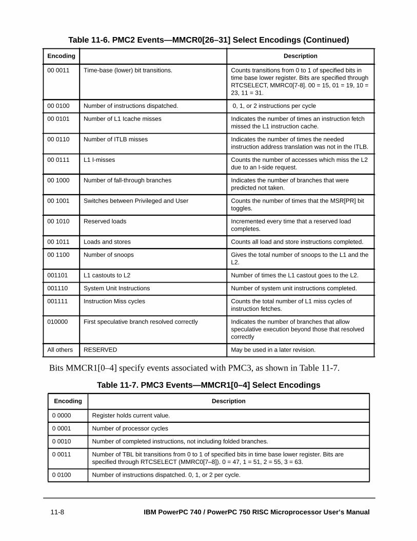
Bits MMCR1[0–4] specify events associated with PMC3, as shown in Table 11-7.
00 0011 Time-base (lower) bit transitions. Counts transitions from 0 to 1 of specified bits intime base lower register. Bits are specified throughRTCSELECT, MMRC0[7-8]. 00 = 15, 01 = 19, 10 =23, 11 = 31.
00 0100 Number of instructions dispatched. 0, 1, or 2 instructions per cycle
00 0101 Number of L1 Icache misses Indicates the number of times an instruction fetchmissed the L1 instruction cache.
00 0110 Number of ITLB misses Indicates the number of times the neededinstruction address translation was not in the ITLB.
00 0111 L1 I-misses Counts the number of accesses which miss the L2due to an I-side request.
00 1000 Number of fall-through branches Indicates the number of branches that werepredicted not taken.
00 1001 Switches between Privileged and User Counts the number of times that the MSR[PR] bittoggles.
00 1010 Reserved loads Incremented every time that a reserved loadcompletes.
00 1011 Loads and stores Counts all load and store instructions completed.
00 1100 Number of snoops Gives the total number of snoops to the L1 and theL2.
001101 L1 castouts to L2 Number of times the L1 castout goes to the L2.
001110 System Unit Instructions Number of system unit instructions completed.
001111 Instruction Miss cycles Counts the total number of L1 miss cycles ofinstruction fetches.
010000 First speculative branch resolved correctly Indicates the number of branches that allowspeculative execution beyond those that resolvedcorrectly
All others RESERVED May be used in a later revision.
Table 11-7. PMC3 Events—MMCR1[0–4] Select Encodings
Encoding Description
0 0000 Register holds current value.
0 0001 Number of processor cycles
0 0010 Number of completed instructions, not including folded branches.
0 0011 Number of TBL bit transitions from 0 to 1 of specified bits in time base lower register. Bits arespecified through RTCSELECT (MMRC0[7–8]). 0 = 47, 1 = 51, 2 = 55, 3 = 63.
0 0100 Number of instructions dispatched. 0, 1, or 2 per cycle.
Table 11-6. PMC2 Events—MMCR0[26–31] Select Encodings (Continued)
Encoding Description
11-8 IBM PowerPC 740 / PowerPC 750 RISC Microprocessor User’s Manual

Bits MMCR1[5–9] specify events associated with PMC4, as shown in Table 11-8.
0 0101 Number of L1 data cache misses. Does not include cache ops.
0 0110 Number of DTLB misses
0 0111 Number of L2 data misses
0 1000 Number of predicted branches that were taken
0 1001 Number of transitions between marked and unmarked processes while in user mode. That is, thenumber of MSR[PM] toggles while the processor is in user mode. RESERVED
0 1010 Number of store conditional instructions completed
0 1011 Number of instructions completed from the FPU
0 1100 Number of L2 castouts caused by snoops to modified lines
0 1101 Number of cache operations that hit in the L2 cache
0 1110 Reserved
0 1111 Number of cycles generated by L1 load misses
1 0000 Number of branches in the second speculative stream that resolve correctly
1 0001 Number of cycles the BPU stalls due to LR or CR unresolved dependencies
All others Reserved. May be used in a later revision.
Table 11-8. PMC4 Events—MMCR1[5–9] Select Encodings
Encoding Comments
00000 Register holds current value
00001 Number of processor cycles
00010 Number of completed instructions, not including folded branches
00011 Number of TBL bit transitions from 0 to 1 of specified bits in time-base lower register. Bits are specifiedthrough RTCSELECT (MMRC0[7–8]). 0 = 47, 1 = 51, 2 = 55, 3 = 63.
00100 Number of instructions dispatched. 0, 1, or 2 per cycle
00101 Number of L2 castouts
00110 Number of cycles spent performing table searches for DTLB accesses.
00111 Reserved. May be used in a later revision.
01000 Number of mispredicted branches. Reserved for future use.
01001 Reserved. May be used in a later revision.
01010 Number of store conditional instructions completed with reservation intact
01011 Number of completed sync instructions
01100 Number of snoop request retries
Table 11-7. PMC3 Events—MMCR1[0–4] Select Encodings (Continued)
Encoding Description
Chapter 11. Performance Monitor 11-9

ad by
ntainsessor.
s thenter to
event,an be
The PMC registers can be accessed with themtspr and mfspr instructions using thefollowing SPR numbers:
• PMC1 is SPR 953• PMC2 is SPR 954• PMC3 is SPR 957• PMC4 is SPR 958
11.2.1.6 User Performance Monitor Counter Registers(UPMC1–UPMC4)
The contents of the PMC1–PMC4 are reflected to UPMC1–UPMC4, which can be reuser-level software. The UPMC registers can be read with themfspr instructions using thefollowing SPR numbers:
• UPMC1 is SPR 937• UPMC2 is SPR 938• UPMC3 is SPR 941• UPMC4 is SPR 942
11.2.1.7 Sampled Instruction Address Register (SIA)The sampled instruction address register (SIA) is a supervisor-level register that cothe effective address of an instruction executing at or around the time that the procsignals the performance monitor interrupt condition. The SIA is shown in Figure 11-4
Figure 11-4. Sampled instruction Address Registers (SIA)
If the performance monitor interrupt is triggered by a threshold event, the SIA containaddress of the exact instruction (called the sampled instruction) that caused the couoverflow.
If the performance monitor interrupt was caused by something besides a thresholdthe SIA contains the address of the last instruction completed during that cycle. SIA caccessed with themtspr andmfspr instructions using SPR 955.
01101 Number of completed integer operations
01110 Number of cycles the BPU cannot process new branches due to having two unresolved branches
11111 Number of L1 Data cache misses. Does not include cache ops.
All others Reserved. May be used in a later revision.
Table 11-8. PMC4 Events—MMCR1[5–9] Select Encodings
Encoding Comments
0 31
Instruction Address
11-10 IBM PowerPC 740 / PowerPC 750 RISC Microprocessor User’s Manual

SIA
cifiedmongrest, ased. Thisstates
or oratchesg is
neratetion
up toused
11.2.1.8 User Sampled Instruction Address Register (USIA)The contents of SIA are reflected to USIA, which can be read by user-level software. Ucan be accessed with themfspr instructions using SPR 939.
11.3 Event CountingCounting can be enabled if conditions in the processor state match a software-specondition. Because a software task scheduler may switch a processor’s execution amultiple processes and because statistics on only a particular process may be of intefacility is provided to mark a process. The performance monitor (PM) bit, MSR[29] is ufor this purpose. System software may set this bit when a marked process is runningenables statistics to be gathered only during the execution of the marked process. Theof MSR[PR] and MSR[PM] together define a state that the processor (supervisprogram) and the process (marked or unmarked) may be in at any time. If this state ma state specified by the MMCR, the state for which monitoring is enabled, countinenabled.
The following are states that can be monitored:
• (Supervisor) only• (User) only• (Marked and user) only• (Not marked and user) only• (Marked and supervisor) only• (Not marked and supervisor) only• (Marked) only• (Not marked) only
In addition, one of two unconditional counting modes may be specified:
• Counting is unconditionally enabled regardless of the states of MSR[PM] andMSR[PR]. This can be accomplished by clearing MMCR0[0–4].
• Counting is unconditionally disabled regardless of the states of MSR[PM] andMSR[PR]. This is done by setting MMCR0[0].
The performance monitor counters count specified events and are used to geperformance monitor exceptions when an overflow (most-significant bit is a 1) situaoccurs. The 750 performance monitor has four, 32-bit registers that can count0x7FFFFFFF (2,147,483,648 in decimal) before overflowing. Bit 0 of the registers isto determine when an interrupt condition exists.
Chapter 11. Performance Monitor 11-11
and
le;
le;
ee
raced,
se7,
o or
eues
ypes
11.4 Event SelectionEvent selection is handled through MMCR0 and MMCR1, described in Table 11-2Table 11-3, respectively. Event selection is described as follows:
• The four event-select fields in MMCR0 and MMCR1 are as follows:
— MMCR0[19–25] PMC1SELECT—PMC1 input selector, 128 events selectab25 defined. See Table 11-5.
— MMCR0[26–31] PMC2SELECT—PMC2 input selector, 64 events selectab21 defined. See Table 11-6.
— MMCR0[0–4] PMC3SELECT—PMC3 input selector. 32 events selectable,defined. See Table 11-7.
— MMCR0[5–9] PMC4SELECT—PMC4 input selector. 32 events selectable. STable 11-8.
• In the tables, a correlation is established between each counter, events to be tand the pattern required for the desired selection.
• The first five events are common to all four counters and are considered to bereference events. These are as follows:
— 00000—Register holds current value
— 00001—Number of processor cycles
— 00010—Number of completed instructions, not including folded branches
— 00011—Number of TBL bit transitions from 0 to 1 of specified bits in time balower register. Bits are specified through RTCSELECT (MMCR0[7–8]). 0 = 41 = 51, 2 = 55, 3 = 63.
— 00100—Number of instructions dispatched. 0, 1, or 2 per cycle
• Some events can have multiple occurrences per cycle, and therefore need twthree bits to represent them.
11.5 NotesThe following warnings should be noted:
• Only those load and store in queue position 0 of their respective load/store quare monitored when a threshold event is selected in PMC1.
• The 750 cannot accurately track threshold events with respect to the following tof loads and stores:
— Unaligned load and store operations that cross a word boundary
— Load and store multiple operations
— Load and store string operations
11-12 IBM PowerPC 740 / PowerPC 750 RISC Microprocessor User’s Manual

s thed by
encel, and-bit
t, are
tical
Appendix APowerPC Instruction Set ListingsA0A0
This appendix lists the PowerPC 750 microprocessor’s instruction set as well aadditional PowerPC instructions not implemented in the 750. Instructions are sortemnemonic, opcode, function, and form. Also included in this appendix is a quick refertable that contains general information, such as the architecture level, privilege leveform, and indicates if the instruction is 64-bit and optional. Note that the 750 is a 32microprocessor, and doesn’t implement any 64-bit instructions.
Note that split fields, that represent the concatenation of sequences from left to righshown in lowercase. For more information refer to Chapter 8, “Instruction Set,” inTheProgramming Environments Manual.
A.1 Instructions Sorted by MnemonicTable A-1 lists the instructions implemented in the PowerPC architecture in alphabeorder by mnemonic.
Table A-1. Complete Instruction List Sorted by Mnemonic
Name 0 5 6 7 8 9 10 11 12 13 14 15 16 17 18 19 20 21 22 23 24 25 26 27 28 29 30 31
addx 31 D A B OE 266 Rc
addc x 31 D A B OE 10 Rc
addex 31 D A B OE 138 Rc
addi 14 D A SIMM
addic 12 D A SIMM
addic. 13 D A SIMM
addis 15 D A SIMM
addme x 31 D A 0 0 0 0 0 OE 234 Rc
addzex 31 D A 0 0 0 0 0 OE 202 Rc
Reserved bits
Key:
Appendix A. PowerPC Instruction Set Listings A-1

andx 31 S A B 28 Rc
andc x 31 S A B 60 Rc
andi. 28 S A UIMM
andis. 29 S A UIMM
bx 18 LI AA LK
bcx 16 BO BI BD AA LK
bcctr x 19 BO BI 0 0 0 0 0 528 LK
bclr x 19 BO BI 0 0 0 0 0 16 LK
cmp 31 crfD 0 L A B 0 0
cmpi 11 crfD 0 L A SIMM
cmpl 31 crfD 0 L A B 32 0
cmpli 10 crfD 0 L A UIMM
cntlzd x 1 31 S A 0 0 0 0 0 58 Rc
cntlzw x 31 S A 0 0 0 0 0 26 Rc
crand 19 crbD crbA crbB 257 0
crandc 19 crbD crbA crbB 129 0
creqv 19 crbD crbA crbB 289 0
crnand 19 crbD crbA crbB 225 0
crnor 19 crbD crbA crbB 33 0
cror 19 crbD crbA crbB 449 0
crorc 19 crbD crbA crbB 417 0
crxor 19 crbD crbA crbB 193 0
dcba 2,7 31 0 0 0 0 0 A B 758 0
dcbf 31 0 0 0 0 0 A B 86 0
dcbi 3 31 0 0 0 0 0 A B 470 0
dcbst 31 0 0 0 0 0 A B 54 0
dcbt 31 0 0 0 0 0 A B 278 0
dcbtst 31 0 0 0 0 0 A B 246 0
dcbz 31 0 0 0 0 0 A B 1014 0
divd x 1 31 D A B OE 489 Rc
divdu x 1 31 D A B OE 457 Rc
divw x 31 D A B OE 491 Rc
divwu x 31 D A B OE 459 Rc
Name 0 5 6 7 8 9 10 11 12 13 14 15 16 17 18 19 20 21 22 23 24 25 26 27 28 29 30 31
A-2 IBM PowerPC 740 / PowerPC 750 RISC Microprocessor User’s Manual

eciwx 31 D A B 310 0
ecowx 31 S A B 438 0
eieio 31 0 0 0 0 0 0 0 0 0 0 0 0 0 0 0 854 0
eqvx 31 S A B 284 Rc
extsb x 31 S A 0 0 0 0 0 954 Rc
extsh x 31 S A 0 0 0 0 0 922 Rc
extsw x 1 31 S A 0 0 0 0 0 986 Rc
fabs x 63 D 0 0 0 0 0 B 264 Rc
fadd x 63 D A B 0 0 0 0 0 21 Rc
fadds x 59 D A B 0 0 0 0 0 21 Rc
fcfid x 1 63 D 0 0 0 0 0 B 846 Rc
fcmpo 63 crfD 0 0 A B 32 0
fcmpu 63 crfD 0 0 A B 0 0
fctid x 1 63 D 0 0 0 0 0 B 814 Rc
fctidz x 1 63 D 0 0 0 0 0 B 815 Rc
fctiw x 63 D 0 0 0 0 0 B 14 Rc
fctiwz x 63 D 0 0 0 0 0 B 15 Rc
fdiv x 63 D A B 0 0 0 0 0 18 Rc
fdivs x 59 D A B 0 0 0 0 0 18 Rc
fmadd x 63 D A B C 29 Rc
fmadds x 59 D A B C 29 Rc
fmr x 63 D 0 0 0 0 0 B 72 Rc
fmsub x 63 D A B C 28 Rc
fmsubs x 59 D A B C 28 Rc
fmul x 63 D A 0 0 0 0 0 C 25 Rc
fmuls x 59 D A 0 0 0 0 0 C 25 Rc
fnabs x 63 D 0 0 0 0 0 B 136 Rc
fneg x 63 D 0 0 0 0 0 B 40 Rc
fnmadd x 63 D A B C 31 Rc
fnmadds x 59 D A B C 31 Rc
fnmsub x 63 D A B C 30 Rc
fnmsubs x 59 D A B C 30 Rc
fres x 2 59 D 0 0 0 0 0 B 0 0 0 0 0 24 Rc
Name 0 5 6 7 8 9 10 11 12 13 14 15 16 17 18 19 20 21 22 23 24 25 26 27 28 29 30 31
Appendix A. PowerPC Instruction Set Listings A-3

frsp x 63 D 0 0 0 0 0 B 12 Rc
frsqrte x 2 63 D 0 0 0 0 0 B 0 0 0 0 0 26 Rc
fsel x 2 63 D A B C 23 Rc
fsqrt x 2,7 63 D 0 0 0 0 0 B 0 0 0 0 0 22 Rc
fsqrts x 2,7 59 D 0 0 0 0 0 B 0 0 0 0 0 22 Rc
fsub x 63 D A B 0 0 0 0 0 20 Rc
fsubs x 59 D A B 0 0 0 0 0 20 Rc
icbi 31 0 0 0 0 0 A B 982 0
isync 19 0 0 0 0 0 0 0 0 0 0 0 0 0 0 0 150 0
lbz 34 D A d
lbzu 35 D A d
lbzux 31 D A B 119 0
lbzx 31 D A B 87 0
ld 1 58 D A ds 0
ldarx 1 31 D A B 84 0
ldu 1 58 D A ds 1
ldux 1 31 D A B 53 0
ldx 1 31 D A B 21 0
lfd 50 D A d
lfdu 51 D A d
lfdux 31 D A B 631 0
lfdx 31 D A B 599 0
lfs 48 D A d
lfsu 49 D A d
lfsux 31 D A B 567 0
lfsx 31 D A B 535 0
lha 42 D A d
lhau 43 D A d
lhaux 31 D A B 375 0
lhax 31 D A B 343 0
lhbrx 31 D A B 790 0
lhz 40 D A d
lhzu 41 D A d
Name 0 5 6 7 8 9 10 11 12 13 14 15 16 17 18 19 20 21 22 23 24 25 26 27 28 29 30 31
A-4 IBM PowerPC 740 / PowerPC 750 RISC Microprocessor User’s Manual

lhzux 31 D A B 311 0
lhzx 31 D A B 279 0
lmw 4 46 D A d
lswi 4 31 D A NB 597 0
lswx 4 31 D A B 533 0
lwa 1 58 D A ds 2
lwarx 31 D A B 20 0
lwaux 1 31 D A B 373 0
lwax 1 31 D A B 341 0
lwbrx 31 D A B 534 0
lwz 32 D A d
lwzu 33 D A d
lwzux 31 D A B 55 0
lwzx 31 D A B 23 0
mcrf 19 crfD 0 0 crfS 0 0 0 0 0 0 0 0 0
mcrfs 63 crfD 0 0 crfS 0 0 0 0 0 0 0 64 0
mcrxr 31 crfD 0 0 0 0 0 0 0 0 0 0 0 0 512 0
mfcr 31 D 0 0 0 0 0 0 0 0 0 0 19 0
mffs x 63 D 0 0 0 0 0 0 0 0 0 0 583 Rc
mfmsr 3 31 D 0 0 0 0 0 0 0 0 0 0 83 0
mfspr 5 31 D spr 339 0
mfsr 3,6 31 D 0 SR 0 0 0 0 0 595 0
mfsrin 3,6 31 D 0 0 0 0 0 B 659 0
mftb 31 D tbr 371 0
mtcrf 31 S 0 CRM 0 144 0
mtfsb0 x 63 crbD 0 0 0 0 0 0 0 0 0 0 70 Rc
mtfsb1 x 63 crbD 0 0 0 0 0 0 0 0 0 0 38 Rc
mtfsf x 63 0 FM 0 B 711 Rc
mtfsfi x 63 crfD 0 0 0 0 0 0 0 IMM 0 134 Rc
mtmsr 3,6 31 S 0 0 0 0 0 0 0 0 0 0 146 0
mtmsrd 1,3 31 S 0 0 0 0 0 0 0 0 0 0 178 0
mtspr 5 31 S spr 467 0
mtsr 3,6 31 S 0 SR 0 0 0 0 0 210 0
Name 0 5 6 7 8 9 10 11 12 13 14 15 16 17 18 19 20 21 22 23 24 25 26 27 28 29 30 31
Appendix A. PowerPC Instruction Set Listings A-5

mtsrd 3,6 31 S 0 SR 0 0 0 0 0 82 0
mtsrdin 3,6 31 S 0 0 0 0 0 B 114 0
mtsrin 3,6 31 S 0 0 0 0 0 B 242 0
mulhd x 1 31 D A B 0 73 Rc
mulhdu x1 31 D A B 0 9 Rc
mulhw x 31 D A B 0 75 Rc
mulhwu x 31 D A B 0 11 Rc
mulld x 1 31 D A B OE 233 Rc
mulli 7 D A SIMM
mullw x 31 D A B OE 235 Rc
nand x 31 S A B 476 Rc
negx 31 D A 0 0 0 0 0 OE 104 Rc
nor x 31 S A B 124 Rc
orx 31 S A B 444 Rc
orc x 31 S A B 412 Rc
ori 24 S A UIMM
oris 25 S A UIMM
rfi 3,6 19 0 0 0 0 0 0 0 0 0 0 0 0 0 0 0 50 0
rfid 1,3 19 0 0 0 0 0 0 0 0 0 0 0 0 0 0 0 18 0
rldcl x 1 30 S A B mb 8 Rc
rldcr x 1 30 S A B me 9 Rc
rldic x 1 30 S A sh mb 2 sh Rc
rldicl x 1 30 S A sh mb 0 sh Rc
rldicr x 1 30 S A sh me 1 sh Rc
rldimi x 1 30 S A sh mb 3 sh Rc
rlwimi x 20 S A SH MB ME Rc
rlwinm x 21 S A SH MB ME Rc
rlwnm x 23 S A B MB ME Rc
sc 17 0 0 0 0 0 0 0 0 0 0 0 0 0 0 0 0 0 0 0 0 0 0 0 0 1 0
slbia 1,2,3 31 0 0 0 0 0 0 0 0 0 0 0 0 0 0 0 498 0
slbie 1,2,3 31 0 0 0 0 0 0 0 0 0 0 B 434 0
sld x 1 31 S A B 27 Rc
slw x 31 S A B 24 Rc
Name 0 5 6 7 8 9 10 11 12 13 14 15 16 17 18 19 20 21 22 23 24 25 26 27 28 29 30 31
A-6 IBM PowerPC 740 / PowerPC 750 RISC Microprocessor User’s Manual

srad x 1 31 S A B 794 Rc
sradi x 1 31 S A sh 413 sh Rc
sraw x 31 S A B 792 Rc
srawi x 31 S A SH 824 Rc
srd x 1 31 S A B 539 Rc
srw x 31 S A B 536 Rc
stb 38 S A d
stbu 39 S A d
stbux 31 S A B 247 0
stbx 31 S A B 215 0
std 1 62 S A ds 0
stdcx. 1 31 S A B 214 1
stdu 1 62 S A ds 1
stdux 1 31 S A B 181 0
stdx 1 31 S A B 149 0
stfd 54 S A d
stfdu 55 S A d
stfdux 31 S A B 759 0
stfdx 31 S A B 727 0
stfiwx 2 31 S A B 983 0
stfs 52 S A d
stfsu 53 S A d
stfsux 31 S A B 695 0
stfsx 31 S A B 663 0
sth 44 S A d
sthbrx 31 S A B 918 0
sthu 45 S A d
sthux 31 S A B 439 0
sthx 31 S A B 407 0
stmw 4 47 S A d
stswi 4 31 S A NB 725 0
stswx 4 31 S A B 661 0
stw 36 S A d
Name 0 5 6 7 8 9 10 11 12 13 14 15 16 17 18 19 20 21 22 23 24 25 26 27 28 29 30 31
Appendix A. PowerPC Instruction Set Listings A-7

stwbrx 31 S A B 662 0
stwcx. 31 S A B 150 1
stwu 37 S A d
stwux 31 S A B 183 0
stwx 31 S A B 151 0
subf x 31 D A B OE 40 Rc
subfc x 31 D A B OE 8 Rc
subfe x 31 D A B OE 136 Rc
subfic 08 D A SIMM
subfme x 31 D A 0 0 0 0 0 OE 232 Rc
subfze x 31 D A 0 0 0 0 0 OE 200 Rc
sync 31 0 0 0 0 0 0 0 0 0 0 0 0 0 0 0 598 0
td 1 31 TO A B 68 0
tdi 1 02 TO A SIMM
tlbia 2,3,7 31 0 0 0 0 0 0 0 0 0 0 0 0 0 0 0 370 0
tlbie 2,3 31 0 0 0 0 0 0 0 0 0 0 B 306 0
tlbsync 2,3 31 0 0 0 0 0 0 0 0 0 0 0 0 0 0 0 566 0
tw 31 TO A B 4 0
twi 03 TO A SIMM
xor x 31 S A B 316 Rc
xori 26 S A UIMM
xoris 27 S A UIMM
Notes :1 64-bit instruction2 Optional instruction3 Supervisor-level instruction4 Load/store string/multiple instruction5 Supervisor- and user-level instruction6 Optional 64-bit bridge instruction7 32-bit instruction not implemented by the PowerPC 750.
Name 0 5 6 7 8 9 10 11 12 13 14 15 16 17 18 19 20 21 22 23 24 25 26 27 28 29 30 31
A-8 IBM PowerPC 740 / PowerPC 750 RISC Microprocessor User’s Manual

r by
A.2 Instructions Sorted by OpcodeTable A-2 lists the instructions defined in the PowerPC architecture in numeric ordeopcode.
Table A-2. Complete Instruction List Sorted by Opcode
Name 0 5 6 7 8 9 10 11 12 13 14 15 16 17 18 19 20 21 22 23 24 25 26 27 28 29 30 31
tdi 1 0 0 0 0 1 0 TO A SIMM
twi 0 0 0 0 1 1 TO A SIMM
mulli 0 0 0 1 1 1 D A SIMM
subfic 0 0 1 0 0 0 D A SIMM
cmpli 0 0 1 0 1 0 crfD 0 L A UIMM
cmpi 0 0 1 0 1 1 crfD 0 L A SIMM
addic 0 0 1 1 0 0 D A SIMM
addic. 0 0 1 1 0 1 D A SIMM
addi 0 0 1 1 1 0 D A SIMM
addis 0 0 1 1 1 1 D A SIMM
bcx 0 1 0 0 0 0 BO BI BD AA LK
sc 0 1 0 0 0 1 0 0 0 0 0 0 0 0 0 0 0 0 0 0 0 0 0 0 0 0 0 0 0 0 0 1 0
bx 0 1 0 0 1 0 LI AA LK
mcrf 0 1 0 0 1 1 crfD 0 0 crfS 0 0 0 0 0 0 0 0 0 0 0 0 0 0 0 0 0 0
bclr x 0 1 0 0 1 1 BO BI 0 0 0 0 0 0 0 0 0 0 1 0 0 0 0 LK
rfid 1,2 0 1 0 0 1 1 0 0 0 0 0 0 0 0 0 0 0 0 0 0 0 0 0 0 0 0 1 0 0 1 0 0
crnor 0 1 0 0 1 1 crbD crbA crbB 0 0 0 0 1 0 0 0 0 1 0
rfi 32,4 0 1 0 0 1 1 0 0 0 0 0 0 0 0 0 0 0 0 0 0 0 0 0 0 0 1 1 0 0 1 0 0
crandc 0 1 0 0 1 1 crbD crbA crbB 0 0 1 0 0 0 0 0 0 1 0
isync 0 1 0 0 1 1 0 0 0 0 0 0 0 0 0 0 0 0 0 0 0 0 0 1 0 0 1 0 1 1 0 0
crxor 0 1 0 0 1 1 crbD crbA crbB 0 0 1 1 0 0 0 0 0 1 0
crnand 0 1 0 0 1 1 crbD crbA crbB 0 0 1 1 1 0 0 0 0 1 0
crand 0 1 0 0 1 1 crbD crbA crbB 0 1 0 0 0 0 0 0 0 1 0
creqv 0 1 0 0 1 1 crbD crbA crbB 0 1 0 0 1 0 0 0 0 1 0
crorc 0 1 0 0 1 1 crbD crbA crbB 0 1 1 0 1 0 0 0 0 1 0
cror 0 1 0 0 1 1 crbD crbA crbB 0 1 1 1 0 0 0 0 0 1 0
Reserved bits
Key:
Appendix A. PowerPC Instruction Set Listings A-9
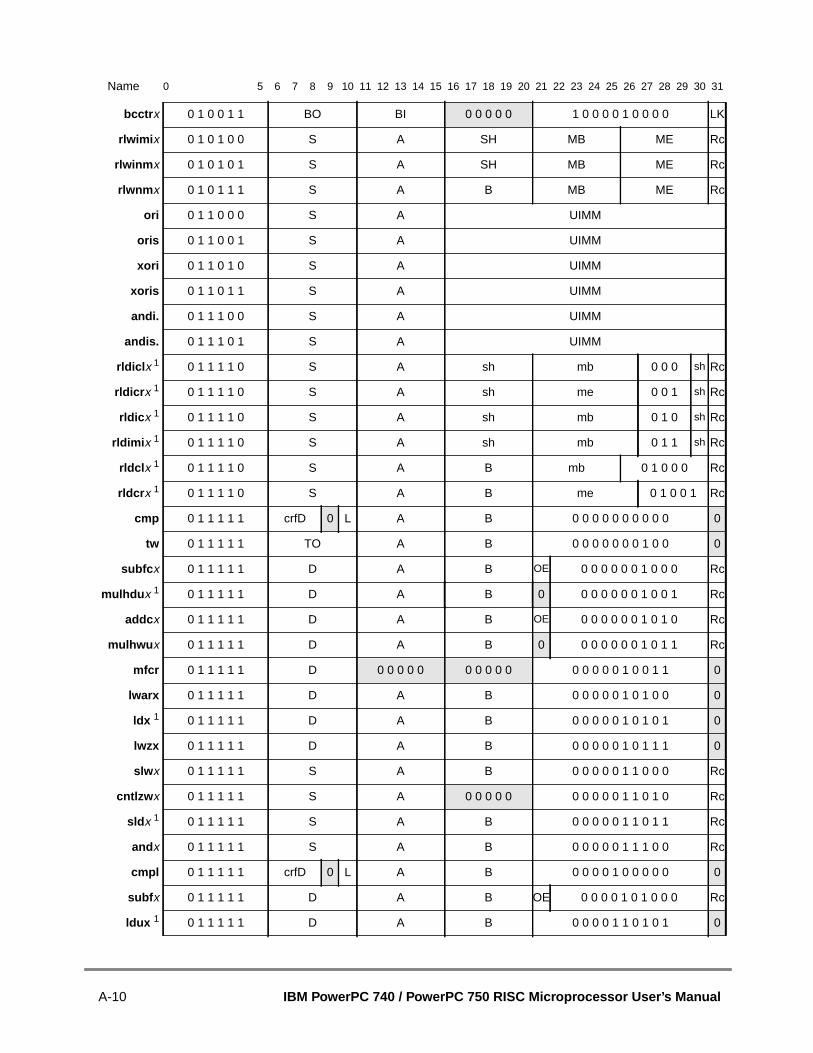
bcctr x 0 1 0 0 1 1 BO BI 0 0 0 0 0 1 0 0 0 0 1 0 0 0 0 LK
rlwimi x 0 1 0 1 0 0 S A SH MB ME Rc
rlwinm x 0 1 0 1 0 1 S A SH MB ME Rc
rlwnm x 0 1 0 1 1 1 S A B MB ME Rc
ori 0 1 1 0 0 0 S A UIMM
oris 0 1 1 0 0 1 S A UIMM
xori 0 1 1 0 1 0 S A UIMM
xoris 0 1 1 0 1 1 S A UIMM
andi. 0 1 1 1 0 0 S A UIMM
andis. 0 1 1 1 0 1 S A UIMM
rldicl x 1 0 1 1 1 1 0 S A sh mb 0 0 0 sh Rc
rldicr x 1 0 1 1 1 1 0 S A sh me 0 0 1 sh Rc
rldic x 1 0 1 1 1 1 0 S A sh mb 0 1 0 sh Rc
rldimi x 1 0 1 1 1 1 0 S A sh mb 0 1 1 sh Rc
rldcl x 1 0 1 1 1 1 0 S A B mb 0 1 0 0 0 Rc
rldcr x 1 0 1 1 1 1 0 S A B me 0 1 0 0 1 Rc
cmp 0 1 1 1 1 1 crfD 0 L A B 0 0 0 0 0 0 0 0 0 0 0
tw 0 1 1 1 1 1 TO A B 0 0 0 0 0 0 0 1 0 0 0
subfc x 0 1 1 1 1 1 D A B OE 0 0 0 0 0 0 1 0 0 0 Rc
mulhdu x 1 0 1 1 1 1 1 D A B 0 0 0 0 0 0 0 1 0 0 1 Rc
addc x 0 1 1 1 1 1 D A B OE 0 0 0 0 0 0 1 0 1 0 Rc
mulhwu x 0 1 1 1 1 1 D A B 0 0 0 0 0 0 0 1 0 1 1 Rc
mfcr 0 1 1 1 1 1 D 0 0 0 0 0 0 0 0 0 0 0 0 0 0 0 1 0 0 1 1 0
lwarx 0 1 1 1 1 1 D A B 0 0 0 0 0 1 0 1 0 0 0
ldx 1 0 1 1 1 1 1 D A B 0 0 0 0 0 1 0 1 0 1 0
lwzx 0 1 1 1 1 1 D A B 0 0 0 0 0 1 0 1 1 1 0
slw x 0 1 1 1 1 1 S A B 0 0 0 0 0 1 1 0 0 0 Rc
cntlzw x 0 1 1 1 1 1 S A 0 0 0 0 0 0 0 0 0 0 1 1 0 1 0 Rc
sld x 1 0 1 1 1 1 1 S A B 0 0 0 0 0 1 1 0 1 1 Rc
andx 0 1 1 1 1 1 S A B 0 0 0 0 0 1 1 1 0 0 Rc
cmpl 0 1 1 1 1 1 crfD 0 L A B 0 0 0 0 1 0 0 0 0 0 0
subf x 0 1 1 1 1 1 D A B OE 0 0 0 0 1 0 1 0 0 0 Rc
ldux 1 0 1 1 1 1 1 D A B 0 0 0 0 1 1 0 1 0 1 0
Name 0 5 6 7 8 9 10 11 12 13 14 15 16 17 18 19 20 21 22 23 24 25 26 27 28 29 30 31
A-10 IBM PowerPC 740 / PowerPC 750 RISC Microprocessor User’s Manual
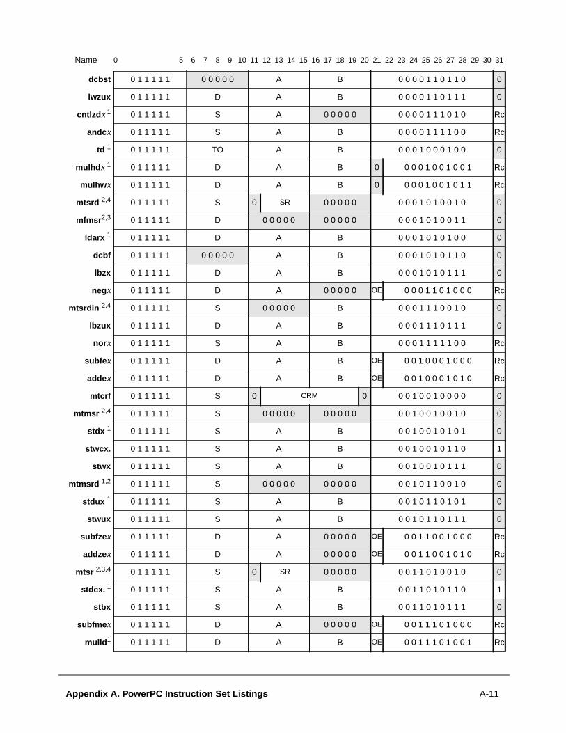
dcbst 0 1 1 1 1 1 0 0 0 0 0 A B 0 0 0 0 1 1 0 1 1 0 0
lwzux 0 1 1 1 1 1 D A B 0 0 0 0 1 1 0 1 1 1 0
cntlzd x 1 0 1 1 1 1 1 S A 0 0 0 0 0 0 0 0 0 1 1 1 0 1 0 Rc
andc x 0 1 1 1 1 1 S A B 0 0 0 0 1 1 1 1 0 0 Rc
td 1 0 1 1 1 1 1 TO A B 0 0 0 1 0 0 0 1 0 0 0
mulhd x 1 0 1 1 1 1 1 D A B 0 0 0 0 1 0 0 1 0 0 1 Rc
mulhw x 0 1 1 1 1 1 D A B 0 0 0 0 1 0 0 1 0 1 1 Rc
mtsrd 2,4 0 1 1 1 1 1 S 0 SR 0 0 0 0 0 0 0 0 1 0 1 0 0 1 0 0
mfmsr 2,3 0 1 1 1 1 1 D 0 0 0 0 0 0 0 0 0 0 0 0 0 1 0 1 0 0 1 1 0
ldarx 1 0 1 1 1 1 1 D A B 0 0 0 1 0 1 0 1 0 0 0
dcbf 0 1 1 1 1 1 0 0 0 0 0 A B 0 0 0 1 0 1 0 1 1 0 0
lbzx 0 1 1 1 1 1 D A B 0 0 0 1 0 1 0 1 1 1 0
negx 0 1 1 1 1 1 D A 0 0 0 0 0 OE 0 0 0 1 1 0 1 0 0 0 Rc
mtsrdin 2,4 0 1 1 1 1 1 S 0 0 0 0 0 B 0 0 0 1 1 1 0 0 1 0 0
lbzux 0 1 1 1 1 1 D A B 0 0 0 1 1 1 0 1 1 1 0
nor x 0 1 1 1 1 1 S A B 0 0 0 1 1 1 1 1 0 0 Rc
subfe x 0 1 1 1 1 1 D A B OE 0 0 1 0 0 0 1 0 0 0 Rc
addex 0 1 1 1 1 1 D A B OE 0 0 1 0 0 0 1 0 1 0 Rc
mtcrf 0 1 1 1 1 1 S 0 CRM 0 0 0 1 0 0 1 0 0 0 0 0
mtmsr 2,4 0 1 1 1 1 1 S 0 0 0 0 0 0 0 0 0 0 0 0 1 0 0 1 0 0 1 0 0
stdx 1 0 1 1 1 1 1 S A B 0 0 1 0 0 1 0 1 0 1 0
stwcx. 0 1 1 1 1 1 S A B 0 0 1 0 0 1 0 1 1 0 1
stwx 0 1 1 1 1 1 S A B 0 0 1 0 0 1 0 1 1 1 0
mtmsrd 1,2 0 1 1 1 1 1 S 0 0 0 0 0 0 0 0 0 0 0 0 1 0 1 1 0 0 1 0 0
stdux 1 0 1 1 1 1 1 S A B 0 0 1 0 1 1 0 1 0 1 0
stwux 0 1 1 1 1 1 S A B 0 0 1 0 1 1 0 1 1 1 0
subfze x 0 1 1 1 1 1 D A 0 0 0 0 0 OE 0 0 1 1 0 0 1 0 0 0 Rc
addzex 0 1 1 1 1 1 D A 0 0 0 0 0 OE 0 0 1 1 0 0 1 0 1 0 Rc
mtsr 2,3,4 0 1 1 1 1 1 S 0 SR 0 0 0 0 0 0 0 1 1 0 1 0 0 1 0 0
stdcx. 1 0 1 1 1 1 1 S A B 0 0 1 1 0 1 0 1 1 0 1
stbx 0 1 1 1 1 1 S A B 0 0 1 1 0 1 0 1 1 1 0
subfme x 0 1 1 1 1 1 D A 0 0 0 0 0 OE 0 0 1 1 1 0 1 0 0 0 Rc
mulld 1 0 1 1 1 1 1 D A B OE 0 0 1 1 1 0 1 0 0 1 Rc
Name 0 5 6 7 8 9 10 11 12 13 14 15 16 17 18 19 20 21 22 23 24 25 26 27 28 29 30 31
Appendix A. PowerPC Instruction Set Listings A-11

addme x 0 1 1 1 1 1 D A 0 0 0 0 0 OE 0 0 1 1 1 0 1 0 1 0 Rc
mullw x 0 1 1 1 1 1 D A B OE 0 0 1 1 1 0 1 0 1 1 Rc
mtsrin 3,2,4 0 1 1 1 1 1 S 0 0 0 0 0 B 0 0 1 1 1 1 0 0 1 0 0
dcbtst 0 1 1 1 1 1 0 0 0 0 0 A B 0 0 1 1 1 1 0 1 1 0 0
stbux 0 1 1 1 1 1 S A B 0 0 1 1 1 1 0 1 1 1 0
addx 0 1 1 1 1 1 D A B OE 0 1 0 0 0 0 1 0 1 0 Rc
dcbt 0 1 1 1 1 1 0 0 0 0 0 A B 0 1 0 0 0 1 0 1 1 0 0
lhzx 0 1 1 1 1 1 D A B 0 1 0 0 0 1 0 1 1 1 0
eqvx 0 1 1 1 1 1 S A B 0 1 0 0 0 1 1 1 0 0 Rc
tlbie 3,2,5 0 1 1 1 1 1 0 0 0 0 0 0 0 0 0 0 B 0 1 0 0 1 1 0 0 1 0 0
eciwx 0 1 1 1 1 1 D A B 0 1 0 0 1 1 0 1 1 0 0
lhzux 0 1 1 1 1 1 D A B 0 1 0 0 1 1 0 1 1 1 0
xor x 0 1 1 1 1 1 S A B 0 1 0 0 1 1 1 1 0 0 Rc
mfspr 6 0 1 1 1 1 1 D spr 0 1 0 1 0 1 0 0 1 1 0
lwax 1 0 1 1 1 1 1 D A B 0 1 0 1 0 1 0 1 0 1 0
lhax 0 1 1 1 1 1 D A B 0 1 0 1 0 1 0 1 1 1 0
tlbia 3,2,5,7 0 1 1 1 1 1 0 0 0 0 0 0 0 0 0 0 0 0 0 0 0 0 1 0 1 1 1 0 0 1 0 0
mftb 0 1 1 1 1 1 D tbr 0 1 0 1 1 1 0 0 1 1 0
lwaux 1 0 1 1 1 1 1 D A B 0 1 0 1 1 1 0 1 0 1 0
lhaux 0 1 1 1 1 1 D A B 0 1 0 1 1 1 0 1 1 1 0
sthx 0 1 1 1 1 1 S A B 0 1 1 0 0 1 0 1 1 1 0
orc x 0 1 1 1 1 1 S A B 0 1 1 0 0 1 1 1 0 0 Rc
sradi x 1 0 1 1 1 1 1 S A sh 1 1 0 0 1 1 1 0 1 1 sh Rc
slbie 1,2,5 0 1 1 1 1 1 0 0 0 0 0 0 0 0 0 0 B 0 1 1 0 1 1 0 0 1 0 0
ecowx 0 1 1 1 1 1 S A B 0 1 1 0 1 1 0 1 1 0 0
sthux 0 1 1 1 1 1 S A B 0 1 1 0 1 1 0 1 1 1 0
orx 0 1 1 1 1 1 S A B 0 1 1 0 1 1 1 1 0 0 Rc
divdu x 1 0 1 1 1 1 1 D A B OE 0 1 1 1 0 0 1 0 0 1 Rc
divwu x 0 1 1 1 1 1 D A B OE 0 1 1 1 0 0 1 0 1 1 Rc
mtspr 6 0 1 1 1 1 1 S spr 0 1 1 1 0 1 0 0 1 1 0
dcbi 2,3 0 1 1 1 1 1 0 0 0 0 0 A B 0 1 1 1 0 1 0 1 1 0 0
nand x 0 1 1 1 1 1 S A B 0 1 1 1 0 1 1 1 0 0 Rc
divd x 1 0 1 1 1 1 1 D A B OE 0 1 1 1 1 0 1 0 0 1 Rc
Name 0 5 6 7 8 9 10 11 12 13 14 15 16 17 18 19 20 21 22 23 24 25 26 27 28 29 30 31
A-12 IBM PowerPC 740 / PowerPC 750 RISC Microprocessor User’s Manual

divw x 0 1 1 1 1 1 D A B OE 0 1 1 1 1 0 1 0 1 1 Rc
slbia 1,2,5 0 1 1 1 1 1 0 0 0 0 0 0 0 0 0 0 0 0 0 0 0 0 1 1 1 1 1 0 0 1 0 0
mcrxr 0 1 1 1 1 1 crfD 0 0 0 0 0 0 0 0 0 0 0 0 1 0 0 0 0 0 0 0 0 0 0
lswx 7 0 1 1 1 1 1 D A B 1 0 0 0 0 1 0 1 0 1 0
lwbrx 0 1 1 1 1 1 D A B 1 0 0 0 0 1 0 1 1 0 0
lfsx 0 1 1 1 1 1 D A B 1 0 0 0 0 1 0 1 1 1 0
srw x 0 1 1 1 1 1 S A B 1 0 0 0 0 1 1 0 0 0 Rc
srd x 1 0 1 1 1 1 1 S A B 1 0 0 0 0 1 1 0 1 1 Rc
tlbsync 3,2,5 0 1 1 1 1 1 0 0 0 0 0 0 0 0 0 0 0 0 0 0 0 1 0 0 0 1 1 0 1 1 0 0
lfsux 0 1 1 1 1 1 D A B 1 0 0 0 1 1 0 1 1 1 0
mfsr 2,4 0 1 1 1 1 1 D 0 SR 0 0 0 0 0 1 0 0 1 0 1 0 0 1 1 0
lswi 7 0 1 1 1 1 1 D A NB 1 0 0 1 0 1 0 1 0 1 0
sync 0 1 1 1 1 1 0 0 0 0 0 0 0 0 0 0 0 0 0 0 0 1 0 0 1 0 1 0 1 1 0 0
lfdx 0 1 1 1 1 1 D A B 1 0 0 1 0 1 0 1 1 1 0
lfdux 0 1 1 1 1 1 D A B 1 0 0 1 1 1 0 1 1 1 0
mfsrin 2,4 0 1 1 1 1 1 D 0 0 0 0 0 B 1 0 1 0 0 1 0 0 1 1 0
stswx 7 0 1 1 1 1 1 S A B 1 0 1 0 0 1 0 1 0 1 0
stwbrx 0 1 1 1 1 1 S A B 1 0 1 0 0 1 0 1 1 0 0
stfsx 0 1 1 1 1 1 S A B 1 0 1 0 0 1 0 1 1 1 0
stfsux 0 1 1 1 1 1 S A B 1 0 1 0 1 1 0 1 1 1 0
stswi 7 0 1 1 1 1 1 S A NB 1 0 1 1 0 1 0 1 0 1 0
stfdx 0 1 1 1 1 1 S A B 1 0 1 1 0 1 0 1 1 1 0
dcba 5,7 0 1 1 1 1 1 0 0 0 0 0 A B 1 0 1 1 1 1 0 1 1 0 0
stfdux 0 1 1 1 1 1 S A B 1 0 1 1 1 1 0 1 1 1 0
lhbrx 0 1 1 1 1 1 D A B 1 1 0 0 0 1 0 1 1 0 0
sraw x 0 1 1 1 1 1 S A B 1 1 0 0 0 1 1 0 0 0 Rc
srad x 1 0 1 1 1 1 1 S A B 1 1 0 0 0 1 1 0 1 0 Rc
srawi x 0 1 1 1 1 1 S A SH 1 1 0 0 1 1 1 0 0 0 Rc
eieio 0 1 1 1 1 1 0 0 0 0 0 0 0 0 0 0 0 0 0 0 0 1 1 0 1 0 1 0 1 1 0 0
sthbrx 0 1 1 1 1 1 S A B 1 1 1 0 0 1 0 1 1 0 0
extsh x 0 1 1 1 1 1 S A 0 0 0 0 0 1 1 1 0 0 1 1 0 1 0 Rc
extsb x 0 1 1 1 1 1 S A 0 0 0 0 0 1 1 1 0 1 1 1 0 1 0 Rc
icbi 0 1 1 1 1 1 0 0 0 0 0 A B 1 1 1 1 0 1 0 1 1 0 0
Name 0 5 6 7 8 9 10 11 12 13 14 15 16 17 18 19 20 21 22 23 24 25 26 27 28 29 30 31
Appendix A. PowerPC Instruction Set Listings A-13
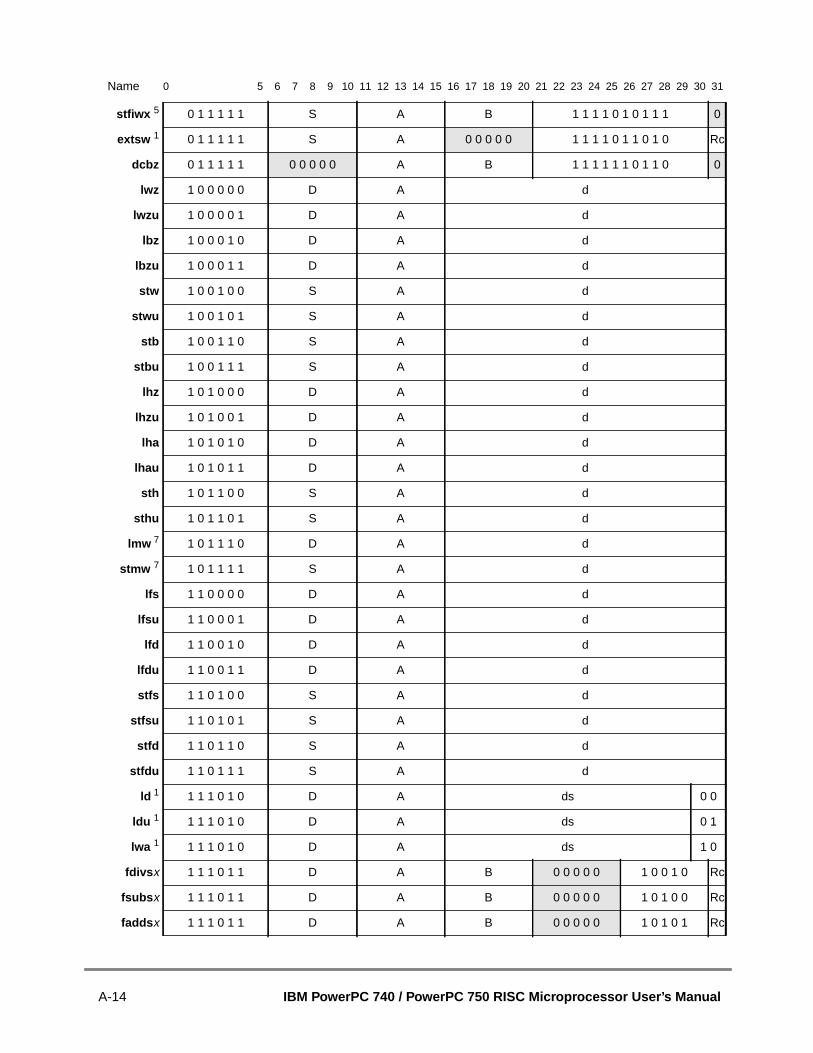
stfiwx 5 0 1 1 1 1 1 S A B 1 1 1 1 0 1 0 1 1 1 0
extsw 1 0 1 1 1 1 1 S A 0 0 0 0 0 1 1 1 1 0 1 1 0 1 0 Rc
dcbz 0 1 1 1 1 1 0 0 0 0 0 A B 1 1 1 1 1 1 0 1 1 0 0
lwz 1 0 0 0 0 0 D A d
lwzu 1 0 0 0 0 1 D A d
lbz 1 0 0 0 1 0 D A d
lbzu 1 0 0 0 1 1 D A d
stw 1 0 0 1 0 0 S A d
stwu 1 0 0 1 0 1 S A d
stb 1 0 0 1 1 0 S A d
stbu 1 0 0 1 1 1 S A d
lhz 1 0 1 0 0 0 D A d
lhzu 1 0 1 0 0 1 D A d
lha 1 0 1 0 1 0 D A d
lhau 1 0 1 0 1 1 D A d
sth 1 0 1 1 0 0 S A d
sthu 1 0 1 1 0 1 S A d
lmw 7 1 0 1 1 1 0 D A d
stmw 7 1 0 1 1 1 1 S A d
lfs 1 1 0 0 0 0 D A d
lfsu 1 1 0 0 0 1 D A d
lfd 1 1 0 0 1 0 D A d
lfdu 1 1 0 0 1 1 D A d
stfs 1 1 0 1 0 0 S A d
stfsu 1 1 0 1 0 1 S A d
stfd 1 1 0 1 1 0 S A d
stfdu 1 1 0 1 1 1 S A d
ld 1 1 1 1 0 1 0 D A ds 0 0
ldu 1 1 1 1 0 1 0 D A ds 0 1
lwa 1 1 1 1 0 1 0 D A ds 1 0
fdivs x 1 1 1 0 1 1 D A B 0 0 0 0 0 1 0 0 1 0 Rc
fsubs x 1 1 1 0 1 1 D A B 0 0 0 0 0 1 0 1 0 0 Rc
fadds x 1 1 1 0 1 1 D A B 0 0 0 0 0 1 0 1 0 1 Rc
Name 0 5 6 7 8 9 10 11 12 13 14 15 16 17 18 19 20 21 22 23 24 25 26 27 28 29 30 31
A-14 IBM PowerPC 740 / PowerPC 750 RISC Microprocessor User’s Manual

fsqrts x 5,7 1 1 1 0 1 1 D 0 0 0 0 0 B 0 0 0 0 0 1 0 1 1 0 Rc
fres x 5 1 1 1 0 1 1 D 0 0 0 0 0 B 0 0 0 0 0 1 1 0 0 0 Rc
fmuls x 1 1 1 0 1 1 D A 0 0 0 0 0 C 1 1 0 0 1 Rc
fmsubs x 1 1 1 0 1 1 D A B C 1 1 1 0 0 Rc
fmadds x 1 1 1 0 1 1 D A B C 1 1 1 0 1 Rc
fnmsubs x 1 1 1 0 1 1 D A B C 1 1 1 1 0 Rc
fnmadds x 1 1 1 0 1 1 D A B C 1 1 1 1 1 Rc
std 1 1 1 1 1 1 0 S A ds 0 0
stdu 1 1 1 1 1 1 0 S A ds 0 1
fcmpu 1 1 1 1 1 1 crfD 0 0 A B 0 0 0 0 0 0 0 0 0 0 0
frsp x 1 1 1 1 1 1 D 0 0 0 0 0 B 0 0 0 0 0 0 1 1 0 0 Rc
fctiw x 1 1 1 1 1 1 D 0 0 0 0 0 B 0 0 0 0 0 0 1 1 1 0
fctiwz x 1 1 1 1 1 1 D 0 0 0 0 0 B 0 0 0 0 0 0 1 1 1 1 Rc
fdiv x 1 1 1 1 1 1 D A B 0 0 0 0 0 1 0 0 1 0 Rc
fsub x 1 1 1 1 1 1 D A B 0 0 0 0 0 1 0 1 0 0 Rc
fadd x 1 1 1 1 1 1 D A B 0 0 0 0 0 1 0 1 0 1 Rc
fsqrt x 5,7 1 1 1 1 1 1 D 0 0 0 0 0 B 0 0 0 0 0 1 0 1 1 0 Rc
fsel x 5 1 1 1 1 1 1 D A B C 1 0 1 1 1 Rc
fmul x 1 1 1 1 1 1 D A 0 0 0 0 0 C 1 1 0 0 1 Rc
frsqrte x 4 1 1 1 1 1 1 D 0 0 0 0 0 B 0 0 0 0 0 1 1 0 1 0 Rc
fmsub x 1 1 1 1 1 1 D A B C 1 1 1 0 0 Rc
fmadd x 1 1 1 1 1 1 D A B C 1 1 1 0 1 Rc
fnmsub x 1 1 1 1 1 1 D A B C 1 1 1 1 0 Rc
fnmadd x 1 1 1 1 1 1 D A B C 1 1 1 1 1 Rc
fcmpo 1 1 1 1 1 1 crfD 0 0 A B 0 0 0 0 1 0 0 0 0 0 0
mtfsb1 x 1 1 1 1 1 1 crbD 0 0 0 0 0 0 0 0 0 0 0 0 0 0 1 0 0 1 1 0 Rc
fneg x 1 1 1 1 1 1 D 0 0 0 0 0 B 0 0 0 0 1 0 1 0 0 0 Rc
mcrfs 1 1 1 1 1 1 crfD 0 0 crfS 0 0 0 0 0 0 0 0 0 0 1 0 0 0 0 0 0 0
mtfsb0 x 1 1 1 1 1 1 crbD 0 0 0 0 0 0 0 0 0 0 0 0 0 1 0 0 0 1 1 0 Rc
fmr x 1 1 1 1 1 1 D 0 0 0 0 0 B 0 0 0 1 0 0 1 0 0 0 Rc
mtfsfi x 1 1 1 1 1 1 crfD 0 0 0 0 0 0 0 IMM 0 0 0 1 0 0 0 0 1 1 0 Rc
fnabs x 1 1 1 1 1 1 D 0 0 0 0 0 B 0 0 1 0 0 0 1 0 0 0 Rc
fabs x 1 1 1 1 1 1 D 0 0 0 0 0 B 0 1 0 0 0 0 1 0 0 0 Rc
Name 0 5 6 7 8 9 10 11 12 13 14 15 16 17 18 19 20 21 22 23 24 25 26 27 28 29 30 31
Appendix A. PowerPC Instruction Set Listings A-15

mffs x 1 1 1 1 1 1 D 0 0 0 0 0 0 0 0 0 0 1 0 0 1 0 0 0 1 1 1 Rc
mtfsf x 1 1 1 1 1 1 0 FM 0 B 1 0 1 1 0 0 0 1 1 1 Rc
fctid x 1 1 1 1 1 1 1 D 0 0 0 0 0 B 1 1 0 0 1 0 1 1 1 0 Rc
fctidz x 1 1 1 1 1 1 1 D 0 0 0 0 0 B 1 1 0 0 1 0 1 1 1 1 Rc
fcfid x 1 1 1 1 1 1 1 D 0 0 0 0 0 B 1 1 0 1 0 0 1 1 1 0 Rc
Notes :1 64-bit instruction2 Supervisor-level instruction3 Supervisor-level instruction4 Optional 64-bit bridge instruction5 Optional instruction6 Supervisor- and user-level instruction7 Load/store string/multiple instruction. 32-bit instruction not implemented by the PowerPC 750.
Name 0 5 6 7 8 9 10 11 12 13 14 15 16 17 18 19 20 21 22 23 24 25 26 27 28 29 30 31
A-16 IBM PowerPC 740 / PowerPC 750 RISC Microprocessor User’s Manual

A.3 Instructions Grouped by Functional CategoriesTable A-3 through Table A-30 list the PowerPC instructions grouped by function.
Table A-3. Integer Arithmetic Instructions
Name 0 5 6 7 8 9 10 11 12 13 14 15 16 17 18 19 20 21 22 23 24 25 26 27 28 29 30 31
addx 31 D A B OE 266 Rc
addc x 31 D A B OE 10 Rc
addex 31 D A B OE 138 Rc
addi 14 D A SIMM
addic 12 D A SIMM
addic. 13 D A SIMM
addis 15 D A SIMM
addme x 31 D A 0 0 0 0 0 OE 234 Rc
addzex 31 D A 0 0 0 0 0 OE 202 Rc
divd x 1
1 64-bit instruction
31 D A B OE 489 Rc
divdu x 1 31 D A B OE 457 Rc
divw x 31 D A B OE 491 Rc
divwu x 31 D A B OE 459 Rc
mulhd x 1 31 D A B 0 73 Rc
mulhdu x1 31 D A B 0 9 Rc
mulhw x 31 D A B 0 75 Rc
mulhwu x 31 D A B 0 11 Rc
mulld 1 31 D A B OE 233 Rc
mulli 07 D A SIMM
mullw x 31 D A B OE 235 Rc
negx 31 D A 0 0 0 0 0 OE 104 Rc
subf x 31 D A B OE 40 Rc
subfc x 31 D A B OE 8 Rc
subfic x 08 D A SIMM
subfe x 31 D A B OE 136 Rc
subfme x 31 D A 0 0 0 0 0 OE 232 Rc
subfze x 31 D A 0 0 0 0 0 OE 200 Rc
Note:
Reserved bitsKey:
Appendix A. PowerPC Instruction Set Listings A-17
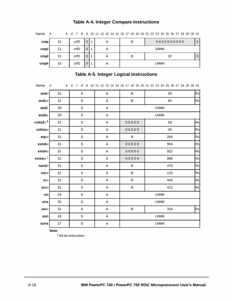
Table A-4. Integer Compare Instructions
Table A-5. Integer Logical Instructions
Name 0 5 6 7 8 9 10 11 12 13 14 15 16 17 18 19 20 21 22 23 24 25 26 27 28 29 30 31
cmp 31 crfD 0 L A B 0 0 0 0 0 0 0 0 0 0 0
cmpi 11 crfD 0 L A SIMM
cmpl 31 crfD 0 L A B 32 0
cmpli 10 crfD 0 L A UIMM
Name 0 5 6 7 8 9 10 11 12 13 14 15 16 17 18 19 20 21 22 23 24 25 26 27 28 29 30 31
andx 31 S A B 28 Rc
andc x 31 S A B 60 Rc
andi. 28 S A UIMM
andis. 29 S A UIMM
cntlzd x 1
1 64-bit instruction
31 S A 0 0 0 0 0 58 Rc
cntlzw x 31 S A 0 0 0 0 0 26 Rc
eqvx 31 S A B 284 Rc
extsb x 31 S A 0 0 0 0 0 954 Rc
extsh x 31 S A 0 0 0 0 0 922 Rc
extsw x 1 31 S A 0 0 0 0 0 986 Rc
nand x 31 S A B 476 Rc
nor x 31 S A B 124 Rc
orx 31 S A B 444 Rc
orc x 31 S A B 412 Rc
ori 24 S A UIMM
oris 25 S A UIMM
xor x 31 S A B 316 Rc
xori 26 S A UIMM
xoris 27 S A UIMM
Note :
A-18 IBM PowerPC 740 / PowerPC 750 RISC Microprocessor User’s Manual

Table A-6. Integer Rotate Instructions
Table A-7. Integer Shift Instructions
Name 0 5 6 7 8 9 10 11 12 13 14 15 16 17 18 19 20 21 22 23 24 25 26 27 28 29 30 31
rldcl x 1
1 64-bit instruction
30 S A B mb 8 Rc
rldcr x 1 30 S A B me 9 Rc
rldic x 1 30 S A sh mb 2 sh Rc
rldicl x 1 30 S A sh mb 0 sh Rc
rldicr x 1 30 S A sh me 1 sh Rc
rldimi x 1 30 S A sh mb 3 sh Rc
rlwimi x 22 S A SH MB ME Rc
rlwinm x 20 S A SH MB ME Rc
rlwnm x 21 S A SH MB ME Rc
Note :
Name 0 5 6 7 8 9 10 11 12 13 14 15 16 17 18 19 20 21 22 23 24 25 26 27 28 29 30 31
sld x 1
1 64-bit instruction
31 S A B 27 Rc
slw x 31 S A B 24 Rc
srad x 1 31 S A B 794 Rc
sradi x 1 31 S A sh 413 sh Rc
sraw x 31 S A B 792 Rc
srawi x 31 S A SH 824 Rc
srd x 1 31 S A B 539 Rc
srw x 31 S A B 536 Rc
Note:
Appendix A. PowerPC Instruction Set Listings A-19

Table A-8. Floating-Point Arithmetic Instructions
Table A-9. Floating-Point Multiply-Add Instructions
Name 0 5 6 7 8 9 10 11 12 13 14 15 16 17 18 19 20 21 22 23 24 25 26 27 28 29 30 31
fadd x 63 D A B 0 0 0 0 0 21 Rc
fadds x 59 D A B 0 0 0 0 0 21 Rc
fdiv x 63 D A B 0 0 0 0 0 18 Rc
fdivs x 59 D A B 0 0 0 0 0 18 Rc
fmul x 63 D A 0 0 0 0 0 C 25 Rc
fmuls x 59 D A 0 0 0 0 0 C 25 Rc
fres x 1
1 Optional instruction2 32-bit instruction not implemented by the PowerPC 750
59 D 0 0 0 0 0 B 0 0 0 0 0 24 Rc
frsqrte x 1 63 D 0 0 0 0 0 B 0 0 0 0 0 26 Rc
fsub x 63 D A B 0 0 0 0 0 20 Rc
fsubs x 59 D A B 0 0 0 0 0 20 Rc
fsel x 1 63 D A B C 23 Rc
fsqrt x 1,2 63 D 0 0 0 0 0 B 0 0 0 0 0 22 Rc
fsqrts x 1,2 59 D 0 0 0 0 0 B 0 0 0 0 0 22 Rc
Note :
Name 0 5 6 7 8 9 10 11 12 13 14 15 16 17 18 19 20 21 22 23 24 25 26 27 28 29 30 31
fmadd x 63 D A B C 29 Rc
fmadds x 59 D A B C 29 Rc
fmsub x 63 D A B C 28 Rc
fmsubs x 59 D A B C 28 Rc
fnmadd x 63 D A B C 31 Rc
fnmadds x 59 D A B C 31 Rc
fnmsub x 63 D A B C 30 Rc
fnmsubs x 59 D A B C 30 Rc
A-20 IBM PowerPC 740 / PowerPC 750 RISC Microprocessor User’s Manual

Table A-10. Floating-Point Rounding and Conversion Instructions
Table A-11. Floating-Point Compare Instructions
Table A-12. Floating-Point Status and Control Register Instructions
Name 0 5 6 7 8 9 10 11 12 13 14 15 16 17 18 19 20 21 22 23 24 25 26 27 28 29 30 31
fcfid x 1
1 64-bit instruction
63 D 0 0 0 0 0 B 846 Rc
fctid x 1 63 D 0 0 0 0 0 B 814 Rc
fctidz x 1 63 D 0 0 0 0 0 B 815 Rc
fctiw x 63 D 0 0 0 0 0 B 14 Rc
fctiwz x 63 D 0 0 0 0 0 B 15 Rc
frsp x 63 D 0 0 0 0 0 B 12 Rc
Note :
Name 0 5 6 7 8 9 10 11 12 13 14 15 16 17 18 19 20 21 22 23 24 25 26 27 28 29 30 31
fcmpo 63 crfD 0 0 A B 32 0
fcmpu 63 crfD 0 0 A B 0 0
Name 0 5 6 7 8 9 10 11 12 13 14 15 16 17 18 19 20 21 22 23 24 25 26 27 28 29 30 31
mcrfs 63 crfD 0 0 crfS 0 0 0 0 0 0 0 64 0
mffs x 63 D 0 0 0 0 0 0 0 0 0 0 583 Rc
mtfsb0 x 63 crbD 0 0 0 0 0 0 0 0 0 0 70 Rc
mtfsb1 x 63 crbD 0 0 0 0 0 0 0 0 0 0 38 Rc
mtfsf x 31 0 FM 0 B 711 Rc
mtfsfi x 63 crfD 0 0 0 0 0 0 0 IMM 0 134 Rc
Appendix A. PowerPC Instruction Set Listings A-21

Table A-13. Integer Load Instructions
Name 0 5 6 7 8 9 10 11 12 13 14 15 16 17 18 19 20 21 22 23 24 25 26 27 28 29 30 31
lbz 34 D A d
lbzu 35 D A d
lbzux 31 D A B 119 0
lbzx 31 D A B 87 0
ld 1
1 64-bit instruction
58 D A ds 0
ldu 1 58 D A ds 1
ldux 1 31 D A B 53 0
ldx 1 31 D A B 21 0
lha 42 D A d
lhau 43 D A d
lhaux 31 D A B 375 0
lhax 31 D A B 343 0
lhz 40 D A d
lhzu 41 D A d
lhzux 31 D A B 311 0
lhzx 31 D A B 279 0
lwa 1 58 D A ds 2
lwaux 1 31 D A B 373 0
lwax 1 31 D A B 341 0
lwz 32 D A d
lwzu 33 D A d
lwzux 31 D A B 55 0
lwzx 31 D A B 23 0
Note:
A-22 IBM PowerPC 740 / PowerPC 750 RISC Microprocessor User’s Manual

Table A-14. Integer Store Instructions
Table A-15. Integer Load and Store with Byte Reverse Instructions
Table A-16. Integer Load and Store Multiple Instructions
Name 0 5 6 7 8 9 10 11 12 13 14 15 16 17 18 19 20 21 22 23 24 25 26 27 28 29 30 31
stb 38 S A d
stbu 39 S A d
stbux 31 S A B 247 0
stbx 31 S A B 215 0
std 1
1 64-bit instruction
62 S A ds 0
stdu 1 62 S A ds 1
stdux 1 31 S A B 181 0
stdx 1 31 S A B 149 0
sth 44 S A d
sthu 45 S A d
sthux 31 S A B 439 0
sthx 31 S A B 407 0
stw 36 S A d
stwu 37 S A d
stwux 31 S A B 183 0
stwx 31 S A B 151 0
Note:
Name 0 5 6 7 8 9 10 11 12 13 14 15 16 17 18 19 20 21 22 23 24 25 26 27 28 29 30 31
lhbrx 31 D A B 790 0
lwbrx 31 D A B 534 0
sthbrx 31 S A B 918 0
stwbrx 31 S A B 662 0
Name 0 5 6 7 8 9 10 11 12 13 14 15 16 17 18 19 20 21 22 23 24 25 26 27 28 29 30 31
lmw 46 D A d
stmw 47 S A d
Note :
Appendix A. PowerPC Instruction Set Listings A-23
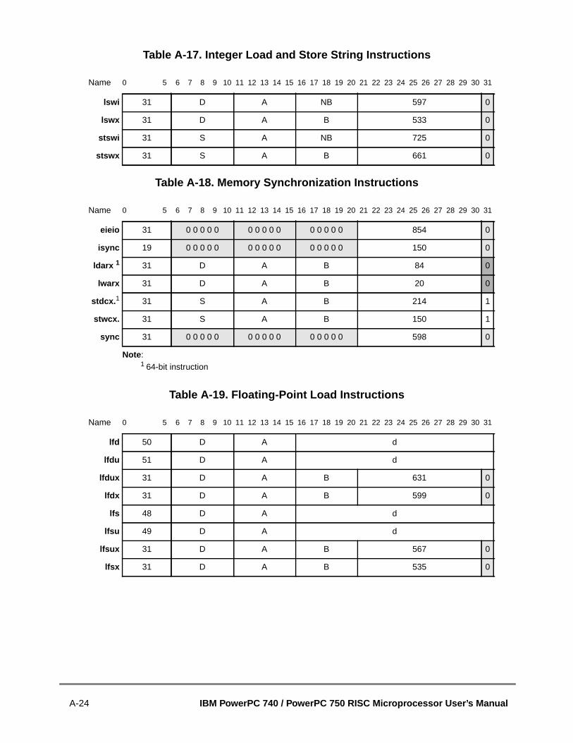
Table A-17. Integer Load and Store String Instructions
Table A-18. Memory Synchronization Instructions
Table A-19. Floating-Point Load Instructions
Name 0 5 6 7 8 9 10 11 12 13 14 15 16 17 18 19 20 21 22 23 24 25 26 27 28 29 30 31
lswi 31 D A NB 597 0
lswx 31 D A B 533 0
stswi 31 S A NB 725 0
stswx 31 S A B 661 0
Name 0 5 6 7 8 9 10 11 12 13 14 15 16 17 18 19 20 21 22 23 24 25 26 27 28 29 30 31
eieio 31 0 0 0 0 0 0 0 0 0 0 0 0 0 0 0 854 0
isync 19 0 0 0 0 0 0 0 0 0 0 0 0 0 0 0 150 0
ldarx 1
1 64-bit instruction
31 D A B 84 0
lwarx 31 D A B 20 0
stdcx. 1 31 S A B 214 1
stwcx. 31 S A B 150 1
sync 31 0 0 0 0 0 0 0 0 0 0 0 0 0 0 0 598 0
Note :
Name 0 5 6 7 8 9 10 11 12 13 14 15 16 17 18 19 20 21 22 23 24 25 26 27 28 29 30 31
lfd 50 D A d
lfdu 51 D A d
lfdux 31 D A B 631 0
lfdx 31 D A B 599 0
lfs 48 D A d
lfsu 49 D A d
lfsux 31 D A B 567 0
lfsx 31 D A B 535 0
A-24 IBM PowerPC 740 / PowerPC 750 RISC Microprocessor User’s Manual

Table A-20. Floating-Point Store Instructions
Table A-21. Floating-Point Move Instructions
Table A-22. Branch Instructions
Name 0 5 6 7 8 9 10 11 12 13 14 15 16 17 18 19 20 21 22 23 24 25 26 27 28 29 30 31
stfd 54 S A d
stfdu 55 S A d
stfdux 31 S A B 759 0
stfdx 31 S A B 727 0
stfiwx 1
1 Optional instruction
31 S A B 983 0
stfs 52 S A d
stfsu 53 S A d
stfsux 31 S A B 695 0
stfsx 31 S A B 663 0
Note :
Name 0 5 6 7 8 9 10 11 12 13 14 15 16 17 18 19 20 21 22 23 24 25 26 27 28 29 30 31
fabs x 63 D 0 0 0 0 0 B 264 Rc
fmr x 63 D 0 0 0 0 0 B 72 Rc
fnabs x 63 D 0 0 0 0 0 B 136 Rc
fneg x 63 D 0 0 0 0 0 B 40 Rc
Name 0 5 6 7 8 9 10 11 12 13 14 15 16 17 18 19 20 21 22 23 24 25 26 27 28 29 30 31
bx 18 LI AA LK
bcx 16 BO BI BD AA LK
bcctr x 19 BO BI 0 0 0 0 0 528 LK
bclr x 19 BO BI 0 0 0 0 0 16 LK
Appendix A. PowerPC Instruction Set Listings A-25

Table A-23. Condition Register Logical Instructions
Table A-24. System Linkage Instructions
Table A-25. Trap Instructions
Name 0 5 6 7 8 9 10 11 12 13 14 15 16 17 18 19 20 21 22 23 24 25 26 27 28 29 30 31
crand 19 crbD crbA crbB 257 0
crandc 19 crbD crbA crbB 129 0
creqv 19 crbD crbA crbB 289 0
crnand 19 crbD crbA crbB 225 0
crnor 19 crbD crbA crbB 33 0
cror 19 crbD crbA crbB 449 0
crorc 19 crbD crbA crbB 417 0
crxor 19 crbD crbA crbB 193 0
mcrf 19 crfD 0 0 crfS 0 0 0 0 0 0 0 0 0 0 0 0 0 0 0 0 0 0
Name 0 5 6 7 8 9 10 11 12 13 14 15 16 17 18 19 20 21 22 23 24 25 26 27 28 29 30 31
rfi 1,2
1 Supervisor-level instruction2 Optional 64-bit bridge instruction
19 0 0 0 0 0 0 0 0 0 0 0 0 0 0 0 50 0
rfid 1,3
3 64-bit instruction
19 0 0 0 0 0 0 0 0 0 0 0 0 0 0 0 18 0
sc 17 0 0 0 0 0 0 0 0 0 0 0 0 0 0 0 0 0 0 0 0 0 0 0 0 0 1 0
Notes :
Name 0 5 6 7 8 9 10 11 12 13 14 15 16 17 18 19 20 21 22 23 24 25 26 27 28 29 30 31
td 1
1 64-bit instruction
31 TO A B 68 0
tdi 1 03 TO A SIMM
tw 31 TO A B 4 0
twi 03 TO A SIMM
Note :
A-26 IBM PowerPC 740 / PowerPC 750 RISC Microprocessor User’s Manual

Table A-26. Processor Control Instructions
Table A-27. Cache Management Instructions
Name 0 5 6 7 8 9 10 11 12 13 14 15 16 17 18 19 20 21 22 23 24 25 26 27 28 29 30 31
mcrxr 31 crfS 0 0 0 0 0 0 0 0 0 0 0 0 512 0
mfcr 31 D 0 0 0 0 0 0 0 0 0 0 19 0
mfmsr 1
1 Supervisor-level instruction
31 D 0 0 0 0 0 0 0 0 0 0 83 0
mfspr 2
2 Supervisor- and user-level instruction
31 D spr 339 0
mftb 31 D tpr 371 0
mtcrf 31 S 0 CRM 0 144 0
mtmsr 1,3
3 Optional 64-bit bridge instruction
31 S 0 0 0 0 0 0 0 0 0 0 146 0
mtmsrd 1,4
4 64-bit instruction
31 S 0 0 0 0 0 0 0 0 0 0 178 0
mtspr 2 31 D spr 467 0
Notes :
Name 0 5 6 7 8 9 10 11 12 13 14 15 16 17 18 19 20 21 22 23 24 25 26 27 28 29 30 31
dcba 1,3
1 Optional instruction
31 0 0 0 0 0 A B 758 0
dcbf 31 0 0 0 0 0 A B 86 0
dcbi 2
2 Supervisor-level instruction3 32-bit instruction not implemented by the PowerPC 750
31 0 0 0 0 0 A B 470 0
dcbst 31 0 0 0 0 0 A B 54 0
dcbt 31 0 0 0 0 0 A B 278 0
dcbtst 31 0 0 0 0 0 A B 246 0
dcbz 31 0 0 0 0 0 A B 1014 0
icbi 31 0 0 0 0 0 A B 982 0
Notes :
Appendix A. PowerPC Instruction Set Listings A-27

Table A-28. Segment Register Manipulation Instructions.
Table A-29. Lookaside Buffer Management Instructions
Table A-30. External Control Instructions
Name 0 5 6 7 8 9 10 11 12 13 14 15 16 17 18 19 20 21 22 23 24 25 26 27 28 29 30 31
mfsr 1,2
1 Supervisor-level instruction2 Optional 64-bit bridge instruction
31 D 0 SR 0 0 0 0 0 595 0
mfsrin 1,2 31 D 0 0 0 0 0 B 659 0
mtsr 1,2 31 S 0 SR 0 0 0 0 0 210 0
mtsrd 1,2 31 S 0 SR 0 0 0 0 0 82 0
mtsrdin 1,2 31 S 0 0 0 0 0 B 114 0
mtsrin 1,2 31 S 0 0 0 0 0 B 242 0
Notes :
Name 0 5 6 7 8 9 10 11 12 13 14 15 16 17 18 19 20 21 22 23 24 25 26 27 28 29 30 31
slbia 1,2,3
1 Supervisor-level instruction2 Optional instruction3 64-bit instruction4 32-bit instruction not implemented by the PowerPC 750
31 0 0 0 0 0 0 0 0 0 0 0 0 0 0 0 498 0
slbie 1,2,3 31 0 0 0 0 0 0 0 0 0 0 B 434 0
tlbia1,2,44,5
4 Supervisor-level instruction5 Optional instruction
31 0 0 0 0 0 0 0 0 0 0 0 0 0 0 0 370 0
tlbie 1,2 4,
531 0 0 0 0 0 0 0 0 0 0 B 306 0
tlbsync 1,2
431 0 0 0 0 0 0 0 0 0 0 0 0 0 0 0 566 0
Notes :
Name 0 5 6 7 8 9 10 11 12 13 14 15 16 17 18 19 20 21 22 23 24 25 26 27 28 29 30 31
eciwx 31 D A B 310 0
ecowx 31 S A B 438 0
A-28 IBM PowerPC 740 / PowerPC 750 RISC Microprocessor User’s Manual

A.4 Instructions Sorted by FormTable A-31 through Table A-45 list the PowerPC instructions grouped by form.
Table A-31. I-Form
Table A-32. B-Form
Table A-33. SC-Form
Table A-34. D-Form
OPCD LI AA LK
Specific Instruction
Name 0 5 6 7 8 9 10 11 12 13 14 15 16 17 18 19 20 21 22 23 24 25 26 27 28 29 30 31
bx 18 LI AA LK
OPCD BO BI BD AA LK
Specific Instruction
Name 0 5 6 7 8 9 10 11 12 13 14 15 16 17 18 19 20 21 22 23 24 25 26 27 28 29 30 31
bcx 16 BO BI BD AA LK
OPCD 0 0 0 0 0 0 0 0 0 0 0 0 0 0 0 0 0 0 0 0 0 0 0 0 0 1 0
Specific Instruction
Name 0 5 6 7 8 9 10 11 12 13 14 15 16 17 18 19 20 21 22 23 24 25 26 27 28 29 30 31
sc 17 0 0 0 0 0 0 0 0 0 0 0 0 0 0 0 0 0 0 0 0 0 0 0 0 0 1 0
OPCD D A d
OPCD D A SIMM
OPCD S A d
OPCD S A UIMM
OPCD crfD 0 L A SIMM
OPCD crfD 0 L A UIMM
OPCD TO A SIMM
Reserved bits
Key:
Appendix A. PowerPC Instruction Set Listings A-29

Specific Instructions
Name 0 5 6 7 8 9 10 11 12 13 14 15 16 17 18 19 20 21 22 23 24 25 26 27 28 29 30 31
addi 14 D A SIMM
addic 12 D A SIMM
addic. 13 D A SIMM
addis 15 D A SIMM
andi. 28 S A UIMM
andis. 29 S A UIMM
cmpi 11 crfD 0 L A SIMM
cmpli 10 crfD 0 L A UIMM
lbz 34 D A d
lbzu 35 D A d
lfd 50 D A d
lfdu 51 D A d
lfs 48 D A d
lfsu 49 D A d
lha 42 D A d
lhau 43 D A d
lhz 40 D A d
lhzu 41 D A d
lmw 1 46 D A d
lwz 32 D A d
lwzu 33 D A d
mulli 7 D A SIMM
ori 24 S A UIMM
oris 25 S A UIMM
stb 38 S A d
stbu 39 S A d
stfd 54 S A d
stfdu 55 S A d
stfs 52 S A d
stfsu 53 S A d
sth 44 S A d
sthu 45 S A d
stmw 1 47 S A d
A-30 IBM PowerPC 740 / PowerPC 750 RISC Microprocessor User’s Manual

Table A-35. DS-Form
Table A-36. X-Form
stw 36 S A d
stwu 37 S A d
subfic 08 D A SIMM
tdi 2 02 TO A SIMM
twi 03 TO A SIMM
xori 26 S A UIMM
xoris 27 S A UIMM
Note :1 Load/store string/multiple instruction2 64-bit instruction
OPCD D A ds XO
OPCD S A ds XO
Specific Instructions
Name 0 5 6 7 8 9 10 11 12 13 14 15 16 17 18 19 20 21 22 23 24 25 26 27 28 29 30 31
ld 1
1 64-bit instruction
58 D A ds 0
ldu 1 58 D A ds 1
lwa 1 58 D A ds 2
std 1 62 S A ds 0
stdu 1 62 S A ds 1
Note :
OPCD D A B XO 0
OPCD D A NB XO 0
OPCD D 0 0 0 0 0 B XO 0
OPCD D 0 0 0 0 0 0 0 0 0 0 XO 0
OPCD D 0 SR 0 0 0 0 0 XO 0
OPCD S A B XO Rc
OPCD S A B XO 1
OPCD S A B XO 0
OPCD S A NB XO 0
OPCD S A 0 0 0 0 0 XO Rc
Appendix A. PowerPC Instruction Set Listings A-31

OPCD S 0 0 0 0 0 B XO 0
OPCD S 0 0 0 0 0 0 0 0 0 0 XO 0
OPCD S 0 SR 0 0 0 0 0 XO 0
OPCD S A SH XO Rc
OPCD crfD 0 L A B XO 0
OPCD crfD 0 0 A B XO 0
OPCD crfD 0 0 crfS 0 0 0 0 0 0 0 XO 0
OPCD crfD 0 0 0 0 0 0 0 0 0 0 0 0 XO 0
OPCD crfD 0 0 0 0 0 0 0 IMM 0 XO Rc
OPCD TO A B XO 0
OPCD D 0 0 0 0 0 B XO Rc
OPCD D 0 0 0 0 0 0 0 0 0 0 XO Rc
OPCD crbD 0 0 0 0 0 0 0 0 0 0 XO Rc
OPCD 0 0 0 0 0 A B XO 0
OPCD 0 0 0 0 0 0 0 0 0 0 B XO 0
OPCD 0 0 0 0 0 0 0 0 0 0 0 0 0 0 0 XO 0
Specific Instructions
Name 0 5 6 7 8 9 10 11 12 13 14 15 16 17 18 19 20 21 22 23 24 25 26 27 28 29 30 31
andx 31 S A B 28 Rc
andc x 31 S A B 60 Rc
cmp 31 crfD 0 L A B 0 0
cmpl 31 crfD 0 L A B 32 0
cntlzd x 1 31 S A 0 0 0 0 0 58 Rc
cntlzw x 31 S A 0 0 0 0 0 26 Rc
dcba 2,6 31 0 0 0 0 0 A B 758 0
dcbf 31 0 0 0 0 0 A B 86 0
dcbi 3 31 0 0 0 0 0 A B 470 0
dcbst 31 0 0 0 0 0 A B 54 0
dcbt 31 0 0 0 0 0 A B 278 0
dcbtst 31 0 0 0 0 0 A B 246 0
dcbz 31 0 0 0 0 0 A B 1014 0
eciwx 31 D A B 310 0
ecowx 31 S A B 438 0
eieio 31 0 0 0 0 0 0 0 0 0 0 0 0 0 0 0 854 0
A-32 IBM PowerPC 740 / PowerPC 750 RISC Microprocessor User’s Manual

eqvx 31 S A B 284 Rc
extsb x 31 S A 0 0 0 0 0 954 Rc
extsh x 31 S A 0 0 0 0 0 922 Rc
extsw x 1 31 S A 0 0 0 0 0 986 Rc
fabs x 63 D 0 0 0 0 0 B 264 Rc
fcfid x 1 63 D 0 0 0 0 0 B 846 Rc
fcmpo 63 crfD 0 0 A B 32 0
fcmpu 63 crfD 0 0 A B 0 0
fctid x 1 63 D 0 0 0 0 0 B 814 Rc
fctidz x 1 63 D 0 0 0 0 0 B 815 Rc
fctiw x 63 D 0 0 0 0 0 B 14 Rc
fctiwz x 63 D 0 0 0 0 0 B 15 Rc
fmr x 63 D 0 0 0 0 0 B 72 Rc
fnabs x 63 D 0 0 0 0 0 B 136 Rc
fneg x 63 D 0 0 0 0 0 B 40 Rc
frsp x 63 D 0 0 0 0 0 B 12 Rc
icbi 31 0 0 0 0 0 A B 982 0
lbzux 31 D A B 119 0
lbzx 31 D A B 87 0
ldarx 1 31 D A B 84 0
ldux 1 31 D A B 53 0
ldx 1 31 D A B 21 0
lfdux 31 D A B 631 0
lfdx 31 D A B 599 0
lfsux 31 D A B 567 0
lfsx 31 D A B 535 0
lhaux 31 D A B 375 0
lhax 31 D A B 343 0
lhbrx 31 D A B 790 0
lhzux 31 D A B 311 0
lhzx 31 D A B 279 0
lswi 4 31 D A NB 597 0
lswx 4 31 D A B 533 0
lwarx 31 D A B 20 0
lwaux 1 31 D A B 373 0
Appendix A. PowerPC Instruction Set Listings A-33

lwax 1 31 D A B 341 0
lwbrx 31 D A B 534 0
lwzux 31 D A B 55 0
lwzx 31 D A B 23 0
mcrfs 63 crfD 0 0 crfS 0 0 0 0 0 0 0 64 0
mcrxr 31 crfD 0 0 0 0 0 0 0 0 0 0 0 0 512 0
mfcr 31 D 0 0 0 0 0 0 0 0 0 0 19 0
mffs x 63 D 0 0 0 0 0 0 0 0 0 0 583 Rc
mfmsr 3 31 D 0 0 0 0 0 0 0 0 0 0 83 0
mfsr 3,5 31 D 0 SR 0 0 0 0 0 595 0
mfsrin 3,5 31 D 0 0 0 0 0 B 659 0
mtfsb0 x 63 crbD 0 0 0 0 0 0 0 0 0 0 70 Rc
mtfsb1 x 63 crfD 0 0 0 0 0 0 0 0 0 0 38 Rc
mtfsfi x 63 crbD 0 0 0 0 0 0 0 IMM 0 134 Rc
mtmsr 3,5 31 S 0 0 0 0 0 0 0 0 0 0 146 0
mtmsrd 1,3 31 S 0 0 0 0 0 0 0 0 0 0 178 0
mtsr 3,5 31 S 0 SR 0 0 0 0 0 210 0
mtsrd 3,5 31 S 0 SR 0 0 0 0 0 82 0
mtsrin 3,5 31 S 0 0 0 0 0 B 242 0
mtsrdin 3,5 31 S 0 0 0 0 0 B 114 0
nand x 31 S A B 476 Rc
nor x 31 S A B 124 Rc
orx 31 S A B 444 Rc
orc x 31 S A B 412 Rc
slbia 1,2,3 31 0 0 0 0 0 0 0 0 0 0 0 0 0 0 0 498 0
slbie 1,2,3 31 0 0 0 0 0 0 0 0 0 0 B 434 0
sld x 1 31 S A B 27 Rc
slw x 31 S A B 24 Rc
srad x 1 31 S A B 794 Rc
sraw x 31 S A B 792 Rc
srawi x 31 S A SH 824 Rc
srd x 1 31 S A B 539 Rc
srw x 31 S A B 536 Rc
stbux 31 S A B 247 0
stbx 31 S A B 215 0
A-34 IBM PowerPC 740 / PowerPC 750 RISC Microprocessor User’s Manual

Ap
pendix A. PowerPC Instruction Set Listings A-35stdcx. 1 31 S A B 214 1
stdux 1 31 S A B 181 0
stdx 1 31 S A B 149 0
stfdux 31 S A B 759 0
stfdx 31 S A B 727 0
stfiwx 2 31 S A B 983 0
stfsux 31 S A B 695 0
stfsx 31 S A B 663 0
sthbrx 31 S A B 918 0
sthux 31 S A B 439 0
sthx 31 S A B 407 0
stswi 4 31 S A NB 725 0
stswx 4 31 S A B 661 0
stwbrx 31 S A B 662 0
stwcx. 31 S A B 150 1
stwux 31 S A B 183 0
stwx 31 S A B 151 0
sync 31 0 0 0 0 0 0 0 0 0 0 0 0 0 0 0 598 0
td 1 31 TO A B 68 0
tlbia 2,3,6 31 0 0 0 0 0 0 0 0 0 0 0 0 0 0 0 370 0
tlbie 2,3 31 0 0 0 0 0 0 0 0 0 0 B 306 0
tlbsync 2,3 31 0 0 0 0 0 0 0 0 0 0 0 0 0 0 0 566 0
tw 31 TO A B 4 0
xor x 31 S A B 316 Rc
Notes :1 64-bit instruction2 Optional instruction3 Supervisor-level instruction4 Load/store string/multiple instruction5 Optional 64-bit bridge instruction6 32-bit instruction not implemented by the PowerPC 750

Table A-37. XL-Form
Table A-38. XFX-Form
OPCD BO BI 0 0 0 0 0 XO LK
OPCD crbD crbA crbB XO 0
OPCD crfD 0 0 crfS 0 0 0 0 0 0 0 XO 0
OPCD 0 0 0 0 0 0 0 0 0 0 0 0 0 0 0 XO 0
Specific Instructions
Name 0 5 6 7 8 9 10 11 12 13 14 15 16 17 18 19 20 21 22 23 24 25 26 27 28 29 30 31
bcctr x 19 BO BI 0 0 0 0 0 528 LK
bclr x 19 BO BI 0 0 0 0 0 16 LK
crand 19 crbD crbA crbB 257 0
crandc 19 crbD crbA crbB 129 0
creqv 19 crbD crbA crbB 289 0
crnand 19 crbD crbA crbB 225 0
crnor 19 crbD crbA crbB 33 0
cror 19 crbD crbA crbB 449 0
crorc 19 crbD crbA crbB 417 0
crxor 19 crbD crbA crbB 193 0
isync 19 0 0 0 0 0 0 0 0 0 0 0 0 0 0 0 150 0
mcrf 19 crfD 0 0 crfS 0 0 0 0 0 0 0 0 0
rfi 1,2
1 Supervisor-level instruction2 Optional 64-bit bridge instruction
19 0 0 0 0 0 0 0 0 0 0 0 0 0 0 0 50 0
rfid 1, 3
3 64-bit instruction
19 0 0 0 0 0 0 0 0 0 0 0 0 0 0 0 18 0
Notes :
OPCD D spr XO 0
OPCD D 0 CRM 0 XO 0
OPCD S spr XO 0
OPCD D tbr XO 0
Specific Instructions
Name 0 5 6 7 8 9 10 11 12 13 14 15 16 17 18 19 20 21 22 23 24 25 26 27 28 29 30 31
mfspr 1 31 D spr 339 0
A-36 IBM PowerPC 740 / PowerPC 750 RISC Microprocessor User’s Manual
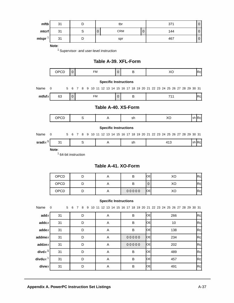
Table A-39. XFL-Form
Table A-40. XS-Form
Table A-41. XO-Form
mftb 31 D tbr 371 0
mtcrf 31 S 0 CRM 0 144 0
mtspr 1 31 D spr 467 0
Note :1 Supervisor- and user-level instruction
OPCD 0 FM 0 B XO Rc
Specific Instructions
Name 0 5 6 7 8 9 10 11 12 13 14 15 16 17 18 19 20 21 22 23 24 25 26 27 28 29 30 31
mtfsf x 63 0 FM 0 B 711 Rc
OPCD S A sh XO sh Rc
Specific Instructions
Name 0 5 6 7 8 9 10 11 12 13 14 15 16 17 18 19 20 21 22 23 24 25 26 27 28 29 30 31
sradi x 1
1 64-bit instruction
31 S A sh 413 sh Rc
Note :
OPCD D A B OE XO Rc
OPCD D A B 0 XO Rc
OPCD D A 0 0 0 0 0 OE XO Rc
Specific Instructions
Name 0 5 6 7 8 9 10 11 12 13 14 15 16 17 18 19 20 21 22 23 24 25 26 27 28 29 30 31
addx 31 D A B OE 266 Rc
addc x 31 D A B OE 10 Rc
addex 31 D A B OE 138 Rc
addme x 31 D A 0 0 0 0 0 OE 234 Rc
addzex 31 D A 0 0 0 0 0 OE 202 Rc
divd x 1 31 D A B OE 489 Rc
divdu x 1 31 D A B OE 457 Rc
divw x 31 D A B OE 491 Rc
Appendix A. PowerPC Instruction Set Listings A-37

Table A-42. A-Form
divwu x 31 D A B OE 459 Rc
mulhd x 1 31 D A B 0 73 Rc
mulhdu x 1 31 D A B 0 9 Rc
mulhw x 31 D A B 0 75 Rc
mulhwu x 31 D A B 0 11 Rc
mulld x 1 31 D A B OE 233 Rc
mullw x 31 D A B OE 235 Rc
negx 31 D A 0 0 0 0 0 OE 104 Rc
subf x 31 D A B OE 40 Rc
subfc x 31 D A B OE 8 Rc
subfe x 31 D A B OE 136 Rc
subfme x 31 D A 0 0 0 0 0 OE 232 Rc
subfze x 31 D A 0 0 0 0 0 OE 200 Rc
Note :1 64-bit instruction
OPCD D A B 0 0 0 0 0 XO Rc
OPCD D A B C XO Rc
OPCD D A 0 0 0 0 0 C XO Rc
OPCD D 0 0 0 0 0 B 0 0 0 0 0 XO Rc
Specific Instructions
Name 0 5 6 7 8 9 10 11 12 13 14 15 16 17 18 19 20 21 22 23 24 25 26 27 28 29 30 31
fadd x 63 D A B 0 0 0 0 0 21 Rc
fadds x 59 D A B 0 0 0 0 0 21 Rc
fdiv x 63 D A B 0 0 0 0 0 18 Rc
fdivs x 59 D A B 0 0 0 0 0 18 Rc
fmadd x 63 D A B C 29 Rc
fmadds x 59 D A B C 29 Rc
fmsub x 63 D A B C 28 Rc
fmsubs x 59 D A B C 28 Rc
fmul x 63 D A 0 0 0 0 0 C 25 Rc
fmuls x 59 D A 0 0 0 0 0 C 25 Rc
fnmadd x 63 D A B C 31 Rc
fnmadds x 59 D A B C 31 Rc
A-38 IBM PowerPC 740 / PowerPC 750 RISC Microprocessor User’s Manual

Table A-43. M-Form
Table A-44. MD-Form
fnmsub x 63 D A B C 30 Rc
fnmsubs x 59 D A B C 30 Rc
fres x 1 59 D 0 0 0 0 0 B 0 0 0 0 0 24 Rc
frsqrte x 1 63 D 0 0 0 0 0 B 0 0 0 0 0 26 Rc
fsel x 1 63 D A B C 23 Rc
fsqrt x 1,2 63 D 0 0 0 0 0 B 0 0 0 0 0 22 Rc
fsqrts x 1,2 59 D 0 0 0 0 0 B 0 0 0 0 0 22 Rc
fsub x 63 D A B 0 0 0 0 0 20 Rc
fsubs x 59 D A B 0 0 0 0 0 20 Rc
Note :1 Optional instruction2 32-bit instruction not implemented by the PowerPC 750
OPCD S A SH MB ME Rc
OPCD S A B MB ME Rc
Specific Instructions
Name 0 5 6 7 8 9 10 11 12 13 14 15 16 17 18 19 20 21 22 23 24 25 26 27 28 29 30 31
rlwimi x 20 S A SH MB ME Rc
rlwinm x 21 S A SH MB ME Rc
rlwnm x 23 S A B MB ME Rc
OPCD S A sh mb XO sh Rc
OPCD S A sh me XO sh Rc
Specific Instructions
Name 0 5 6 7 8 9 10 11 12 13 14 15 16 17 18 19 20 21 22 23 24 25 26 27 28 29 30 31
rldic x 1
1 64-bit instruction
30 S A sh mb 2 sh Rc
rldicl x 1 30 S A sh mb 0 sh Rc
rldicr x 1 30 S A sh me 1 sh Rc
rldimi x 1 30 S A sh mb 3 sh Rc
Note :
Appendix A. PowerPC Instruction Set Listings A-39

Table A-45. MDS-Form
OPCD S A B mb XO Rc
OPCD S A B me XO Rc
Specific Instructions
Name 0 5 6 7 8 9 10 11 12 13 14 15 16 17 18 19 20 21 22 23 24 25 26 27 28 29 30 31
rldcl x 1
1 64-bit instruction
30 S A B mb 8 Rc
rldcr x 1 30 S A B me 9 Rc
Note :
A-40 IBM PowerPC 740 / PowerPC 750 RISC Microprocessor User’s Manual

such
A.5 Instruction Set LegendTable A-46Table A-47 provides general information on the PowerPC instruction set (as the architectural level, privilege level, and form).
Table A-46. PowerPC Instruction Set Legend
UISA VEA OEA Supervisor Level Optional Form
addx XO
addc x XO
addex XO
addi D
addic D
addic. D
addis D
addmex XO
addzex XO
andx X
andc x X
andi. D
andis. D
bx I
bcx B
bcctr x XL
bclr x XL
cmp X
cmpi D
cmpl X
cmpli D
cntlzw x X
crand XL
crandc XL
creqv XL
crnand XL
crnor XL
cror XL
crorc XL
Appendix A. PowerPC Instruction Set Listings A-41

crxor XL
dcba X
dcbf X
dcbi X
dcbst X
dcbt X
dcbtst X
dcbz X
divw x XO
divwu x XO
eciwx X
ecowx X
eieio X
eqvx X
extsb x X
extsh x X
fabs x X
fadd x A
fadds x A
fcmpo X
fcmpu X
fctiw x X
fctiwz x X
fdiv x A
fdivs x A
fmadd x A
fmadds x A
fmr x X
fmsub x A
fmsubs x A
fmul x A
fmuls x A
Table A-46. PowerPC Instruction Set Legend (Continued)
UISA VEA OEA Supervisor Level Optional Form
A-42 IBM PowerPC 740 / PowerPC 750 RISC Microprocessor User’s Manual

fnabs x X
fneg x X
fnmadd x A
fnmadds x A
fnmsub x A
fnmsubs x A
fres x A
frsp x X
frsqrte x A
fsel x A
fsqrt x A
fsqrts x A
fsub x A
fsubs x A
icbi X
isync XL
lbz D
lbzu D
lbzux X
lbzx X
lfd D
lfdu D
lfdux X
lfdx X
lfs D
lfsu D
lfsux X
lfsx X
lha D
lhau D
lhaux X
lhax X
Table A-46. PowerPC Instruction Set Legend (Continued)
UISA VEA OEA Supervisor Level Optional Form
Appendix A. PowerPC Instruction Set Listings A-43

lhbrx X
lhz D
lhzu D
lhzux X
lhzx X
lmw 2 D
lswi 2 X
lswx 2 X
lwarx X
lwbrx X
lwz D
lwzu D
lwzux X
lwzx X
mcrf XL
mcrfs X
mcrxr X
mfcr X
mffs X
mfmsr X
mfspr 1 XFX
mfsr X
mfsrin X
mftb XFX
mtcrf XFX
mtfsb0 x X
mtfsb1 x X
mtfsf x XFL
mtfsfi x X
mtmsr X
mtspr 1 XFX
mtsr X
Table A-46. PowerPC Instruction Set Legend (Continued)
UISA VEA OEA Supervisor Level Optional Form
A-44 IBM PowerPC 740 / PowerPC 750 RISC Microprocessor User’s Manual
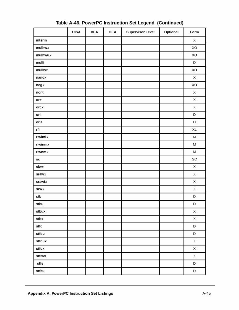
mtsrin X
mulhw x XO
mulhwu x XO
mulli D
mullw x XO
nand x X
negx XO
nor x X
orx X
orc x X
ori D
oris D
rfi XL
rlwimi x M
rlwinm x M
rlwnm x M
sc SC
slw x X
sraw x X
srawi x X
srw x X
stb D
stbu D
stbux X
stbx X
stfd D
stfdu D
stfdux X
stfdx X
stfiwx X
stfs D
stfsu D
Table A-46. PowerPC Instruction Set Legend (Continued)
UISA VEA OEA Supervisor Level Optional Form
Appendix A. PowerPC Instruction Set Listings A-45

stfsux X
stfsx X
sth D
sthbrx X
sthu D
sthux X
sthx X
stmw 2 D
stswi 2 X
stswx 2 X
stw D
stwbrx X
stwcx. X
stwu D
stwux X
stwx X
subf x XO
subfc x XO
subfe x XO
subfic D
subfme x XO
subfze x XO
sync X
tlbia x X
tlbie x X
tlbsync X
tw X
twi D
xor x X
Table A-46. PowerPC Instruction Set Legend (Continued)
UISA VEA OEA Supervisor Level Optional Form
A-46 IBM PowerPC 740 / PowerPC 750 RISC Microprocessor User’s Manual

1 Supervisor- and user-level instruction2 Load/store string or multiple instruction3 Optional instruction provided to support temporary 64-bit bridge4 Defined for the 32-bit architecture and by the temporary 64-bit bridge
xori D
xoris D
Notes:
Table A-47. PowerPC Instruction Set Legend
UISA VEA OEASupervisor
Level64-BitOnly
64-BitBridge
Optional Form
addx XO
addc x XO
addex XO
addi D
addic D
addic. D
addis D
addmex XO
addzex XO
andx X
andc x X
andi. D
andis. D
bx I
bcx B
bcctr x XL
bclr x XL
cmp X
cmpi D
cmpl X
cmpli D
cntlzd x X
Table A-46. PowerPC Instruction Set Legend (Continued)
UISA VEA OEA Supervisor Level Optional Form
Appendix A. PowerPC Instruction Set Listings A-47

cntlzw x X
crand XL
crandc XL
creqv XL
crnand XL
crnor XL
cror XL
crorc XL
crxor XL
dcba 3 X
dcbf X
dcbi X
dcbst X
dcbt X
dcbtst X
dcbz X
divd x XO
divdu x XO
divw x XO
divwu x XO
eciwx X
ecowx X
eieio X
eqvx X
extsb x X
extsh x X
extsw x X
fabs x X
fadd x A
fadds x A
fcfid x X
fcmpo X
Table A-47. PowerPC Instruction Set Legend (Continued)
UISA VEA OEASupervisor
Level64-BitOnly
64-BitBridge
Optional Form
A-48 IBM PowerPC 740 / PowerPC 750 RISC Microprocessor User’s Manual

fcmpu X
fctid x X
fctidz x X
fctiw x X
fctiwz x X
fdiv x A
fdivs x A
fmadd x A
fmadds x A
fmr x X
fmsub x A
fmsubs x A
fmul x A
fmuls x A
fnabs x X
fneg x X
fnmadd x A
fnmadds x A
fnmsub x A
fnmsubs x A
fres x A
frsp x X
frsqrte x A
fsel x A
fsqrt x 3 A
fsqrts x 3 A
fsub x A
fsubs x A
icbi X
isync XL
lbz D
lbzu D
Table A-47. PowerPC Instruction Set Legend (Continued)
UISA VEA OEASupervisor
Level64-BitOnly
64-BitBridge
Optional Form
Appendix A. PowerPC Instruction Set Listings A-49

lbzux X
lbzx X
ld DS
ldarx X
ldu DS
ldux X
ldx X
lfd D
lfdu D
lfdux X
lfdx X
lfs D
lfsu D
lfsux X
lfsx X
lha D
lhau D
lhaux X
lhax X
lhbrx X
lhz D
lhzu D
lhzux X
lhzx X
lmw 2 D
lswi 2 X
lswx 2 X
lwa DS
lwarx X
lwaux X
lwax X
lwbrx X
Table A-47. PowerPC Instruction Set Legend (Continued)
UISA VEA OEASupervisor
Level64-BitOnly
64-BitBridge
Optional Form
A-50 IBM PowerPC 740 / PowerPC 750 RISC Microprocessor User’s Manual

lwz D
lwzu D
lwzux X
lwzx X
mcrf XL
mcrfs X
mcrxr X
mfcr X
mffs X
mfmsr X
mfspr 1 XFX
mfsr 4 X
mfsrin 4 X
mftb XFX
mtcrf XFX
mtfsb0 x X
mtfsb1 x X
mtfsf x XFL
mtfsfi x X
mtmsr 4 X
mtmsrd X
mtspr 1 XFX
mtsr 4 X
mtsrd 4 X
mtsrdin 4 X
mtsrin 4 X
mulhd x XO
mulhdu x XO
mulhw x XO
mulhwu x XO
mulld x XO
mulli D
Table A-47. PowerPC Instruction Set Legend (Continued)
UISA VEA OEASupervisor
Level64-BitOnly
64-BitBridge
Optional Form
Appendix A. PowerPC Instruction Set Listings A-51

mullw x XO
nand x X
negx XO
nor x X
orx X
orc x X
ori D
oris D
rfi 4 XL
rfid XL
rldcl x MDS
rldcr x MDS
rldic x MD
rldicl x MD
rldicr x MD
rldimi x MD
rlwimi x M
rlwinm x M
rlwnm x M
sc SC
slbia X
slbie X
sld x X
slw x X
srad x X
sradi x XS
sraw x X
srawi x X
srd x X
srw x X
stb D
stbu D
Table A-47. PowerPC Instruction Set Legend (Continued)
UISA VEA OEASupervisor
Level64-BitOnly
64-BitBridge
Optional Form
A-52 IBM PowerPC 740 / PowerPC 750 RISC Microprocessor User’s Manual
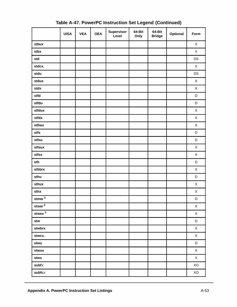
stbux X
stbx X
std DS
stdcx. X
stdu DS
stdux X
stdx X
stfd D
stfdu D
stfdux X
stfdx X
stfiwx X
stfs D
stfsu D
stfsux X
stfsx X
sth D
sthbrx X
sthu D
sthux X
sthx X
stmw 2 D
stswi 2 X
stswx 2 X
stw D
stwbrx X
stwcx. X
stwu D
stwux X
stwx X
subf x XO
subfc x XO
Table A-47. PowerPC Instruction Set Legend (Continued)
UISA VEA OEASupervisor
Level64-BitOnly
64-BitBridge
Optional Form
Appendix A. PowerPC Instruction Set Listings A-53

1 Supervisor- and user-level instruction2 Load/store string or multiple instruction3 32-bit instruction not implemented by the PowerPC 7504 Instruction is optional for 64-bit implementations only
subfe x XO
subfic D
subfme x XO
subfze x XO
sync X
td X
tdi D
tlbia x3 X
tlbie x X
tlbsync X
tw X
twi D
xor x X
xori D
xoris D
Notes:
Table A-47. PowerPC Instruction Set Legend (Continued)
UISA VEA OEASupervisor
Level64-BitOnly
64-BitBridge
Optional Form
A-54 IBM PowerPC 740 / PowerPC 750 RISC Microprocessor User’s Manual

notecutetionation.
erPC
Appendix BInstructions Not Implemented
B.1 Lists of InstructionsB0B0
This appendix provides a list of the 32-bit and 64-bit PowerPC instructions that areimplemented in the PowerPC 750 microprocessor. Note that any attempt to exinstructions that are not implemented on the 750 will generate an illegal instrucexception. Note that exceptions are referred to as interrupts in the architecture specific
Table B-1 provides the 32-bit PowerPC instructions that are optional to the Powarchitecture but not implemented by the 750.
Table B-2 provides a list of 64-bit instructions that are not implemented by the 750.
Table B-1. 32-Bit Instructions Not Implemented
Mnemonic Instruction
dcba Data Cache Block Allocate
fsqrt Floating Square Root (Double-Precision)
fsqrts Floating Square Root Single
tlbia TLB Invalidate All
Table B-2. 64-Bit Instructions Not Implemented
Mnemonic Instruction
cntlzd Count Leading Zeros Double Word
divd Divide Double Word
divdu Divide Double Word Unsigned
extsw Extend Sign Word
fcfid Floating Convert From Integer Double Word
fctid Floating Convert to Integer Double Word
fctidz Floating Convert to Integer Double Word with Round toward Zero
ld Load Double Word
ldarx Load Double Word and Reserve Indexed
Appendix B. Instructions Not Implemented B-1
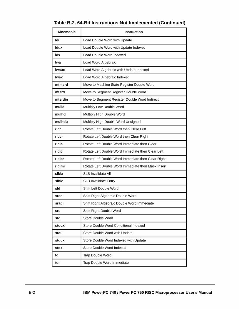
ldu Load Double Word with Update
ldux Load Double Word with Update Indexed
ldx Load Double Word Indexed
lwa Load Word Algebraic
lwaux Load Word Algebraic with Update Indexed
lwax Load Word Algebraic Indexed
mtmsrd Move to Machine State Register Double Word
mtsrd Move to Segment Register Double Word
mtsrdin Move to Segment Register Double Word Indirect
mulld Multiply Low Double Word
mulhd Multiply High Double Word
mulhdu Multiply High Double Word Unsigned
rldcl Rotate Left Double Word then Clear Left
rldcr Rotate Left Double Word then Clear Right
rldic Rotate Left Double Word Immediate then Clear
rldicl Rotate Left Double Word Immediate then Clear Left
rldicr Rotate Left Double Word Immediate then Clear Right
rldimi Rotate Left Double Word Immediate then Mask Insert
slbia SLB Invalidate All
slbie SLB Invalidate Entry
sld Shift Left Double Word
srad Shift Right Algebraic Double Word
sradi Shift Right Algebraic Double Word Immediate
srd Shift Right Double Word
std Store Double Word
stdcx. Store Double Word Conditional Indexed
stdu Store Double Word with Update
stdux Store Double Word Indexed with Update
stdx Store Double Word Indexed
td Trap Double Word
tdi Trap Double Word Immediate
Table B-2. 64-Bit Instructions Not Implemented (Continued)
Mnemonic Instruction
B-2 IBM PowerPC 740 / PowerPC 750 RISC Microprocessor User’s Manual

in this
EEE.
orr or
s a
toous
tiondress
Thethe
nteses.
f a
0
56are
Glossary of Terms and Abbreviations
G.1 Alphabetical ListThe glossary contains an alphabetical list of terms, phrases, and abbreviations usedbook. Some of the terms and definitions included in the glossary are reprinted fromIEEEStd 754-1985, IEEE Standard for Binary Floating-Point Arithmetic, copyright ©1985 bythe Institute of Electrical and Electronics Engineers, Inc. with the permission of the I
Architecture. A detailed specification of requirements for a processorcomputer system. It does not specify details of how the processocomputer system must be implemented; instead it providetemplate for a family of compatibleimplementations.
Asynchronous exception. Exceptionsthat are caused by events externalthe processor’s execution. In this document, the term ‘asynchronexception’ is used interchangeably with the wordinterrupt.
Atomic access. A bus access that attempts to be part of a read-write operato the same address uninterrupted by any other access to that ad(the term refers to the fact that the transactions are indivisible).PowerPC architecture implements atomic accesses throughlwarx /stwcx. instruction pair.
BAT (block address translation) mechanism. A software-controlled arraythat stores the available block address translations on-chip.
Biased exponent. An exponentwhose range of values is shifted by a consta(bias). Typically a bias is provided to allow a range of positive valuto express a range that includes both positive and negative valu
Big-endian. A byte-ordering method in memory where the address n oword corresponds to themost-significant byte. In an addressedmemory word, the bytes are ordered (left to right) 0, 1, 2, 3, withbeing the most-significant byte.See Little-endian.
Block. (Memory) An area of memory that ranges from 128 Kbyte to 2Mbyte whose size, translation, and protection attributescontrolled by theBAT mechanism(see Cache Block).
A
B
Glossary of Terms and Abbreviations Glossary-1

rely-ngame
r fors ofbe
beenons,re
chn a
bermis
s for
otcanasay
n). Iftheare
he
o a
d/or
Boundedly undefined. A characteristic of certain operation results that anot rigidly prescribed by the PowerPC architecture. Boundedundefined results for a given operation may vary amoimplementations and between execution attempts in the simplementation.
Although the architecture does not prescribe the exact behaviowhen results are allowed to be boundedly undefined, the resultexecuting instructions in contexts where results are allowed toboundedly undefined are constrained to ones that could haveachieved by executing an arbitrary sequence of defined instructiin valid form, starting in the state the machine was in befoattempting to execute the given instruction.
Branch folding. The replacement with target instructions of a braninstruction and any instructions along the not-taken path whebranch is either taken or predicted as taken.
Branch prediction—The process of guessing whether a branch willtaken. Such predictions can be correct or incorrect; the te‘predicted’ as it is used here does not imply that the predictioncorrect (successful). The PowerPC architecture defines a meanstatic branch prediction as part of the instruction encoding.
Branch resolution—The determination of whether a branch is taken or ntaken. A branch is said to be resolved when the processordetermine which instruction path to take. If the branch is resolvedpredicted, the instructions following the predicted branch that mhave been speculatively executed can complete (see completiothe branch is not resolved as predicted, instructions onmispredicted path, and any results of speculative execution,purged from the pipeline and fetching continues from tnonpredicted path.
Burst. A multiple-beat data transfer whose total size is typically equal tcache block.
Cache. High-speed memory containing recently accessed data aninstructions (subset of main memory).
C
Glossary-2 IBM PowerPC 740 / PowerPC 750 RISC Microprocessor User’s Manual

mg
s.ith
oforyfromalue
aifiedain
che
iss
medit.
edtheeedno
inan
xtionsion
Cache block. A small region of contiguous memory that is copied fromemory into acache. The size of a cache block may vary amonprocessors; the maximum block size is onepage. In PowerPCprocessors,cache coherencyis maintained on a cache-block basiNote that the term ‘cache block’ is often used interchangeably w‘cache line’.
Cache coherency. An attribute wherein an accurate and common viewmemory is provided to all devices that share the same memsystem. Caches are coherent if a processor performing a readits cache is supplied with data corresponding to the most recent vwritten to memory or to another processor’s cache.
Cache flush. An operation that removes from a cache any data fromspecified address range. This operation ensures that any moddata within the specified address range is written back to mmemory. This operation is generated typically by a Data CaBlock Flush (dcbf) instruction.
Caching-inhibited. A memory update policy in which thecacheis bypassedand the load or store is performed to or from main memory.
Cast-outs. Cache blocksthat must be written to memory when a cache mcauses a cache block to be replaced.
Changed bit. One of twopage history bitsfound in eachpage table entry(PTE). The processor sets the changed bit if any store is perforinto thepage. See alsoPage access history bits and Referenced b
Clear. To cause a bit or bit field to register a value of zero.See alsoSet.
Completion—Completion occurs when an instruction has finishexecuting, written back any results, and is removed fromcompletion queue. When an instruction completes, it is guarantthat this instruction and all previous instructions can causeexceptions.
Context synchronization. An operation that ensures that all instructionsexecution complete past the point where they can produceexception, that all instructions in execution complete in the contein which they began execution, and that all subsequent instructarefetchedand executed in the new context. Context synchronizatmay result from executing specific instructions (such asisyncor rfi )or when certain events occur (such as an exception).
Copy-back. An operation in which modified data in acache blockis copiedback to memory.
Glossary of Terms and Abbreviations Glossary-3

ntose
ankly
re,U
.
cial,
ishat(thatThetionthe
s
tiontothe
hewerhe
Chewedsm,n a
Denormalized number. A nonzero floating-point number whose exponehas a reserved value, usually the format's minimum, and whexplicit or implicit leading significand bit is zero.
Direct-mapped cache. A cache in which each main memory address cappear in only one location within the cache, operates more quicwhen the memory request is a cache hit.
Effective address (EA). The 32- or 64-bit address specified for a load, stoor an instruction fetch. This address is then submitted to the MMfor translation to either aphysical memoryaddress or an I/O address
Exception. A condition encountered by the processor that requires spesupervisor-level processing.
Exception handler. A software routine that executes when an exceptiontaken. Normally, the exception handler corrects the condition tcaused the exception, or performs some other meaningful taskmay include aborting the program that caused the exception).address for each exception handler is identified by an excepvector offset defined by the architecture and a prefix selected viaMSR.
Exclusive state.MEI state (E) in which only one caching device containdata that is also in system memory.
Execution synchronization. A mechanism by which all instructions inexecution are architecturally complete before beginning execu(appearing to begin execution) of the next instruction. Similarcontext synchronization but doesn't force the contents ofinstruction buffers to be deleted and refetched.
Exponent. In the binary representation of a floating-point number, texponent is the component that normally signifies the integer poto which the value two is raised in determining the value of trepresented number.See alsoBiased exponent.
Fall-through (branch fall-through) —A not-taken branch. On the PowerP750, fall-through branch instructions are removed from tinstruction stream at dispatch. That is, these instructions are alloto fall through the instruction queue via the dispatch mechaniwithout either being passed to an execution unit and or giveposition in the completion queue.
D
E
F
Glossary-4 IBM PowerPC 740 / PowerPC 750 RISC Microprocessor User’s Manual

nd
tandnsata
ing-
and
of
l-s andns.tore
n at be
for
csnary
anotbitbit-bitbit
Fetch. Retrieving instructions from either the cache or main memory aplacing them into the instruction queue.
Floating-point register (FPR). Any of the 32 registers in the floating-poinregister file. These registers provide the source operandsdestination results for floating-point instructions. Load instructiomove data from memory to FPRs and store instructions move dfrom FPRs to memory. The FPRs are 64 bits wide and store floatpoint values in double-precision format
Flush. An operation that causes a modified cache block to be invalidatedthe data to be written to memory.
Fraction. In the binary representation of a floating-point number, the fieldthesignificand that lies to the right of its implied binary point.
General-purpose register (GPR). Any of the 32 registers in the generapurpose register file. These registers provide the source operanddestination results for all integer data manipulation instructioInteger load instructions move data from memory to GPRs and sinstructions move data from GPRs to memory.
Guarded. The guarded attribute pertains to out-of-order execution. Whepage is designated as guarded, instructions and data cannoaccessed out-of-order.
Harvard architecture . An architectural model featuring separate cachesinstruction and data.
Hashing. An algorithm used in thepage table search process.
IEEE 754. A standard written by the Institute of Electrical and ElectroniEngineers that defines operations and representations of bifloating-point numbers.
Illegal instructions. A class of instructions that are not implemented forparticular PowerPC processor. These include instructionsdefined by the PowerPC architecture. In addition, for 32-implementations, instructions that are defined only for 64-implementations are considered to be illegal instructions. For 64implementations instructions that are defined only for 32-implementations are considered to be illegal instructions.
G
H
HI
Glossary of Terms and Abbreviations Glossary-5

Cntndas
be
nt
er
. Anis
ion
ute
ts
alid
sterr or
ata
er,
Implementation. A particular processor that conforms to the PowerParchitecture, but may differ from other architecture-compliaimplementations for example in design, feature set, aimplementation ofoptional features. The PowerPC architecture hmany different implementations.
Imprecise exception. A type ofsynchronous exceptionthat is allowed not toadhere to the precise exception model (seePrecise exception). ThePowerPC architecture allows only floating-point exceptions tohandled imprecisely.
Instruction queue. A holding place for instructions fetched from the curreinstruction stream.
Integer unit . A functional unit in the 750 responsible for executing integinstructions.
In-order. An aspect of an operation that adheres to a sequential modeloperation is said to be performed in-order if, at the time that itperformed, it is known to be required by the sequential executmodel.See Out-of-order.
Instruction latency. The total number of clock cycles necessary to execan instruction and make ready the results of that instruction.
Interrupt . An asynchronous exception. On PowerPC processors, interrupare a special case of exceptions.See also asynchronous exception.
Invalid state. State of a cache entry that does not currently contain a vcopy of a cache block from memory.
Key bits. A set of key bits referred to as Ks and Kp in each segment regiand each BAT register. The key bits determine whether supervisouser programs can access apage within thatsegment or block.
Kill . An operation that causes acache block to be invalidated.
L2 cache. SeeSecondary cache.
Least-significant bit (lsb). The bit of least value in an address, register, delement, or instruction encoding.
Least-significant byte (LSB). The byte of least value in an address, registdata element, or instruction encoding.
K
LL
Glossary-6 IBM PowerPC 740 / PowerPC 750 RISC Microprocessor User’s Manual
3
tem.the
rhich
lockthat
ntem
cthip
f,s.
ceernal
rs,
s,
inNs
ters
Little-endian . A byte-ordering method in memory where the addressn of aword corresponds to theleast-significant byte. In an addressedmemory word, the bytes are ordered (left to right) 3, 2, 1, 0, withbeing themost-significant byte. See Big-endian.
MESI (modified/exclusive/shared/invalid). Cache coherencyprotocol usedto manage caches on different devices that share a memory sysNote that the PowerPC architecture does not specifyimplementation of a MESI protocol to ensure cache coherency.
Memory access ordering. The specific order in which the processoperforms load and store memory accesses and the order in wthose accesses complete.
Memory-mapped accesses. Accesses whose addresses use the page or baddress translation mechanisms provided by the MMU andoccur externally with the bus protocol defined for memory.
Memory coherency. An aspect of caching in which it is ensured that aaccurate view of memory is provided to all devices that share sysmemory.
Memory consistency. Refers to agreement of levels of memory with respeto a single processor and system memory (for example, on-ccache, secondary cache, and system memory).
Memory management unit (MMU). The functional unit that is capable otranslating aneffective (logical) address to a physical addressproviding protection mechanisms, and defining caching method
Modified state. MEI state (M) in which one, and only one, caching devihas the valid data for that address. The data at this address in extmemory is not valid.See MESI.
Most-significant bit (msb). The highest-order bit in an address, registedata element, or instruction encoding.
Most-significant byte (MSB). The highest-order byte in an addresregisters, data element, or instruction encoding.
NaN. An abbreviation for not a number; a symbolic entity encodedfloating-point format. There are two types of NaNs—signaling Naand quiet NaNs.
No-op. No-operation. A single-cycle operation that does not affect regisor generate bus activity.
M
N
Glossary of Terms and Abbreviations Glossary-7

ediatetothe
isor-tionevelEA
at isbe
adforbe
ot
dthe
theForbe
of
setrite
Normalization. A process by which a floating-point value is manipulatsuch that it can be represented in the format for the approprprecision (single- or double-precision). For a floating-point valuebe representable in the single- or double-precision format,leading implied bit must be a 1.
OEA (operating environment architecture). The level of the architecturethat describes PowerPC memory management model, supervlevel registers, synchronization requirements, and the excepmodel. It also defines the time-base feature from a supervisor-lperspective. Implementations that conform to the PowerPC Oalso conform to the PowerPC UISA and VEA.
Optional. A feature, such as an instruction, a register, or an exception, thdefined by the PowerPC architecture but not required toimplemented.
Out-of-order. An aspect of an operation that allows it to be performed aheof one that may have preceded it in the sequential model,example, speculative operations. An operation is said toperformed out-of-order if, at the time that it is performed, it is nknown to be required by the sequential execution model.SeeIn-order.
Out-of-order execution. A technique that allows instructions to be issueand completed in an order that differs from their sequence ininstruction stream.
Overflow. An condition that occurs during arithmetic operations whenresult cannot be stored accurately in the destination register(s).example, if two 32-bit numbers are multiplied, the result may notrepresentable in 32 bits.
Packet. A term used in the 750 with respect to direct-store operations.
Page. A region in memory. The OEA defines a page as a 4-Kbyte areamemory, aligned on a 4-Kbyte boundary.
Page access history bits. Thechangedandreferencedbits in the PTE keeptrack of the access history within the page. The referenced bit isby the MMU whenever the page is accessed for a read or woperation. The changed bit is set when the page is stored into.SeeChanged bit and Referenced bit.
O
P
Glossary-8 IBM PowerPC 740 / PowerPC 750 RISC Microprocessor User’s Manual

sorin a
a
trysize
toesor
the
ionuresthe
ecanand
n
ATonly
ptionised tobe
Page fault. A page fault is a condition that occurs when the procesattempts to access a memory location that does not reside withpage not currently resident inphysical memory. On PowerPCprocessors, a page fault exception condition occurs whenmatching, validpage table entry(PTE[V] = 1) cannot be located.
Page table. A table in memory is comprised ofpage table entries, or PTEs.It is further organized into eight PTEs per PTEG (page table engroup). The number of PTEGs in the page table depends on theof the page table (as specified in the SDR1 register).
Page table entry (PTE). Data structures containing information usedtranslateeffective addressto physical address on a 4-Kbyte pagbasis. A PTE consists of 8 bytes of information in a 32-bit procesand 16 bytes of information in a 64-bit processor.
Physical memory. The actual memory that can be accessed throughsystem’s memory bus.
Pipelining. A technique that breaks operations, such as instructprocessing or bus transactions, into smaller distinct stages or ten(respectively) so that a subsequent operation can begin beforeprevious one has completed.
Precise exceptions. A category of exception for which the pipeline can bstopped so instructions that preceded the faulting instructioncomplete, and subsequent instructions can be flushedredispatched after exception handling has completed.SeeImpreciseexceptions.
Primary opcode. The most-significant 6 bits (bits 0–5) of the instructioencoding that identifies the type of instruction. See Secondaryopcode.
Protection boundary. A boundary betweenprotection domains.
Protection domain. A protection domain is a segment, a virtual page, a Barea, or a range of unmapped effective addresses. It is definedwhen the appropriate relocate bit in the MSR (IR or DR) is 1.
Quiesce. To come to rest. The processor is said to quiesce when an exceis taken or async instruction is executed. The instruction streamstopped at the decode stage and executing instructions are allowcomplete to create a controlled context for instructions that mayaffected by out-of-order, parallel execution. SeeContextsynchronization.
Q
Glossary of Terms and Abbreviations Glossary-9
ticto
alid
rce
rce.
s a
rce.
iseressled
t,the
R
of a
srget
Quiet NaN. A type of NaN that can propagate through most arithmeoperations without signaling exceptions. A quiet NaN is usedrepresent the results of certain invalid operations, such as invarithmetic operations on infinities or on NaNs, when invalid.SeeSignaling NaN.
rA . TherA instruction field is used to specify a GPR to be used as a souor destination.
rB . TherB instruction field is used to specify a GPR to be used as a sou
rD . The rD instruction field is used to specify a GPR to be used adestination.
rS. TherS instruction field is used to specify a GPR to be used as a sou
Real address mode. An MMU mode when no address translationperformed and theeffective addressspecified is the same as thphysical address. The processor’s MMU is operating in real addmode if its ability to perform address translation has been disabthrough the MSR registers IR and/or DR bits.
Record bit. Bit 31 (or the Rc bit) in the instruction encoding. When it is seupdates the condition register (CR) to reflect the result ofoperation.
Referenced bit. One of twopage history bitsfound in eachpage table entry(PTE). The processor sets thereferenced bitwhenever the page isaccessed for a read or write.See alsoPage access history bits.
Register indirect addressing. A form of addressing that specifies one GPthat contains the address for the load or store.
Register indirect with immediate index addressing. A form of addressingthat specifies an immediate value to be added to the contentsspecified GPR to form the target address for the load or store.
Register indirect with index addressing. A form of addressing that specifiethat the contents of two GPRs be added together to yield the taaddress for the load or store.
Reservation. The processor establishes a reservation on acache blockofmemory space when it executes anlwarx instruction to read amemory semaphore into a GPR.
R
Glossary-10 IBM PowerPC 740 / PowerPC 750 RISC Microprocessor User’s Manual
dory
ery behe.
of a
ener-to the
isaset,
m
ists
re
n thethe
d for
n
RISC (reduced instruction set computing). An architecturecharacterizedby fixed-length instructions with nonoverlapping functionality anby a separate set of load and store instructions that perform memaccesses.
Secondary cache. A cache memory that is typically larger and has a longaccess time than the primary cache. A secondary cache mashared by multiple devices. Also referred to as L2, or level-2, cac
Set(v). To write a nonzero value to a bit or bit field; the opposite ofclear. Theterm ‘set’ may also be used to generally describe the updatingbit or bit field.
Set (n). A subdivision of acache. Cacheable data can be stored in a givlocation in any one of the sets, typically corresponding to its loworder address bits. Because several memory locations can mapsame location, cached data is typically placed in the set whosecacheblockcorresponding to that address was used least recently.SeeSet-associative.
Set-associative. Aspect of cache organization in which the cache spacedivided into sections, calledsets. The cache controller associatesparticular main memory address with the contents of a particularor region, within the cache.
Signaling NaN. A type of NaN that generates an invalid operation prograexception when it is specified as arithmetic operands.SeeQuietNaN.
Significand. The component of a binary floating-point number that consof an explicit or implicit leading bit to the left of its implied binarypoint and a fraction field to the right.
Simplified mnemonics. Assembler mnemonics that represent a mocomplex form of a common operation.
Slave. The device addressed by a master device. The slave is identified iaddress tenure and is responsible for supplying or latchingrequested data for the master during the data tenure.
Snooping. Monitoring addresses driven by a bus master to detect the neecoherency actions.
Snoop push. Write-backs due to a snoop hit. The block will transition to ainvalid or exclusive state.
S
Glossary of Terms and Abbreviations Glossary-11

nse
om
,n a
s
Incanmory
fpes
tion.es.
sed
tionata
thendend
Split-transaction. A transaction with independent request and respotenures.
Split-transaction bus. A bus that allows address and data transactions frdifferent processors to occur independently.
Static branch prediction. Mechanism by which software (for examplecompilers) can hint to the machine hardware about the directiobranch is likely to take.
Superscalar machine. A machine that can issue multiple instructionconcurrently from a conventional linear instruction stream.
Supervisor mode. The privileged operation state of a processor.supervisor mode, software, typically the operating system,access all control registers and can access the supervisor mespace, among other privileged operations.
Synchronization.A process to ensure that operations occur strictlyin order.See Context synchronization and Execution synchronization.
Synchronous exception.An exceptionthat is generated by the execution oa particular instruction or instruction sequence. There are two tyof synchronous exceptions,precise andimprecise.
System memory.The physical memory available to a processor.
Tenure. A tenure consists of three phases: arbitration, transfer, terminaThere can be separate address bus tenures and data bus tenur
TLB (translation lookaside buffer) A cache that holds recently-usedpagetable entries.
Throughput . The measure of the number of instructions that are procesper clock cycle.
Transaction. A complete exchange between two bus devices. A transacis minimally comprised of an address tenure; one or more dtenures may be involved in the exchange.
Transfer termination . Signal that refers to both signals that acknowledgetransfer of individual beats (of both single-beat transfer aindividual beats of a burst transfer) and to signals that mark theof the tenure.
T
Glossary-12 IBM PowerPC 740 / PowerPC 750 RISC Microprocessor User’s Manual

thepes,
by
heister.ns
her
tiontrolged
.
pleodel,ility
rily
an
mentis
lested
ite
UISA (user instruction set architecture). The level of the architecture towhich user-level software should conform. The UISA definesbase user-level instruction set, user-level registers, data tyfloating-point memory conventions and exception model as seenuser programs, and the memory and programming models.
Underflow. A condition that occurs during arithmetic operations when tresult cannot be represented accurately in the destination regFor example, underflow can happen if two floating-point fractioare multiplied and the result requires a smallerexponentand/ormantissa than the single-precision format can provide. In otwords, the result is too small to be represented accurately.
User mode. The operating state of a processor used typically by applicasoftware. In user mode, software can access only certain conregisters and can access only user memory space. No privileoperations can be performed. Also referred to as problem state
VEA (virtual environment architecture) . The level of thearchitecturethatdescribes the memory model for an environment in which multidevices can access memory, defines aspects of the cache mdefines cache control instructions, and defines the time-base facfrom a user-level perspective.Implementationsthat conform to thePowerPC VEA also adhere to the UISA, but may not necessaadhere to the OEA.
Virtual address. An intermediate address used in the translation ofeffective address to a physical address.
Virtual memory . The address space created using the memory managefacilities of the processor. Program access to virtual memorypossible only when it coincides withphysical memory.
Word . A 32-bit data element.
Write-back . A cache memory update policy in which processor write cycare directly written only to the cache. External memory is updaonly indirectly, for example, when a modified cache block iscast outto make room for newer data.
Write-through . A cache memory update policy in which all processor wrcycles are written to both the cache and memory.
U
V
VW
Glossary of Terms and Abbreviations Glossary-13

Glossary-14 IBM PowerPC 740 / PowerPC 750 RISC Microprocessor User’s Manual
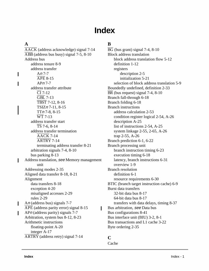
Index
AAACK (address acknowledge) signal 7-14ABB (address bus busy) signal 7-5, 8-10Address bus
address tenure 8-9address transfer
An 7-7APE 8-15APn 7-7
address transfer attributeCI 7-12GBL 7-13TBST 7-12, 8-16TSIZn 7-11, 8-15TTn 7-8, 8-15WT 7-13
address transfer startTS 7-6, 8-14
address transfer terminationAACK 7-14ARTRY 7-14terminating address transfer 8-21
arbitration signals 7-4, 8-10bus parking 8-13
Address translation,see Memory managementunit
Addressing modes 2-35Aligned data transfer 8-18, 8-21Alignment
data transfers 8-18exception 4-20misaligned accesses 2-29rules 2-29
An (address bus) signals 7-7APE (address parity error) signal 8-15APn (address parity) signals 7-7Arbitration, system bus 8-12, 8-23Arithmetic instructions
floating-point A-20integer A-17
ARTRY (address retry) signal 7-14
BBG (bus grant) signal 7-4, 8-10Block address translation
block address translation flow 5-12definition 1-12registers
description 2-5initialization 5-21
selection of block address translation 5-9Boundedly undefined, definition 2-33BR (bus request) signal 7-4, 8-10Branch fall-through 6-18Branch folding 6-18Branch instructions
address calculation 2-53condition register logical 2-54, A-26description A-25list of instructions 2-54, A-25system linkage 2-55, 2-65, A-26trap 2-55, A-26
Branch prediction 6-1, 6-22Branch processing unit
branch instruction timing 6-23execution timing 6-18latency, branch instructions 6-31overview 1-9
Branch resolutiondefinition 6-1resource requirements 6-30
BTIC (branch target instruction cache) 6-9Burst data transfers
32-bit data bus 8-1764-bit data bus 8-17transfers with data delays, timing 8-37
Bus arbitration,see Data busBus configurations 8-41Bus interface unit (BIU) 3-2, 8-1Bus transactions and L1 cache 3-22Byte ordering 2-35
CCache
Index Index - 1

3-
2,
0
bus interface unit 3-2, 8-1cache arbitration 6-11cache block, definition 3-3cache characteristics 3-1cache coherency
description 3-5overview 3-25reaction to bus operations 3-26
cache control 3-13cache control instructions
bus operations 3-24cache control 3-13dcbi 2-66dcbt 2-63
cache hit 6-11cache integration 3-2cache management instructions A-27cache miss 6-14cache operations
cache block push operations 9-4data cache transactions 3-22instruction cache block fill 3-21load/store operations, processor initiat-
ed 3-10operations 3-18overview 3-1, 8-3snoop response to bus transactions 3-26
cache unit overview 3-3cache-inhibited accesses (I bit) 3-6data cache configuration 3-3dcbf/dcbst execution 9-4icbi 9-4instruction cache configuration 3-4instruction cache throttling 10-10L1 cache and bus transactions 3-22L2 interface
cache configuration 9-2cache global invalidation 9-7cache initialization 9-6cache testing 9-8clock configuration 9-9dcbi 9-4eieio 9-4L2 cache considerations 6-15L2 cache interface signals 7-25operation 9-2
overview 9-1SRAM timing examples 9-9stwcx. execution 9-4sync 9-4
load/store operations, processor initiated10
PLRU replacement 3-19stwcx. execution 9-4
Changed (C) bit maintenance recording 5-15-23
Checkstopsignal 7-22, 8-42state 4-19
CI (cache inhibit) signal 7-12CKSTP_IN/CKSTP_OUT<Default Para
Font (checkstop input/output) sig-nals> 7-22
Classes of instructions 2-32Clean block operation 3-27CLK_OUT signal 7-29Clock signals
PLL_CFGn 7-30SYSCLK 7-29
Compare instructionsfloating-point A-21integer A-18
Completioncompletion unit resource requirements 6-3considerations 6-16definition 6-1
Context synchronization 2-36Conventions xxx, xxxiv, 6-1COP/scan interface 8-44Copy-back mode 6-27CR (condition register)
CR logical instructions 2-54, A-26CR, description 2-3
CTR register 2-4
DDABR (data address breakpoint register) 2-7DAR (data address register) 2-6Data bus
arbitration signals 7-15, 8-10bus arbitration 8-23data tenure 8-9
Index - 2 IBM PowerPC 740 / PowerPC 750 RISC Microprocessor User’s Manual

-
4-
data transfer 7-17, 8-25data transfer termination 7-19, 8-26
Data cacheblock push operation 3-22configuration 3-3DCFI, DCE, DLOCK bits 3-13organization 3-4
Data organization in memory 2-28Data transfers
alignment 8-18burst ordering 8-17eciwx and ecowx instructions, alignment 8-
21operand conventions 2-28signals 8-25
DBB (data bus busy) signal 7-16, 8-10, 8-24DBDIS (data bus disable) signal 7-19DBG (data bus grant) signal 7-15, 8-10DBWO (data bus write only) signal 7-16, 8-10,
8-25, 8-45dcbi 2-66dcbt 2-63DEC (decrementer register) 2-7Decrementer exception 4-21Defined instruction class 2-33DHn/DLn (data bus) signals 7-17Dispatch
considerations 6-16dispatch unit resource requirements 6-30
DPn (data bus parity) signals 7-18DRTRY (data retry) signal 7-20, 8-26, 8-29DSI exception 4-19DSISR register 2-6DTLB organization 5-25Dynamic branch prediction 6-9
EEAR (external access register) 2-7Effective address calculation
address translation 5-4branches 2-35loads and stores 2-35, 2-46, 2-51
eieio 2-62EMI protocol, enforcing memory coherency 8-
30
Enveloped high-priority cache block push operation 3-22
Error termination 8-30Event counting 11-11Event selection 11-12Exceptions
alignment exception 4-20decrementer exception 4-21definitions 4-12DSI exception 4-19enabling and disabling exceptions 4-10exception classes 4-2exception prefix (IP) bit 4-13exception priorities 4-4exception processing 4-7, 4-10external interrupt 4-20FP assist exception 4-22FP unavailable exception 4-21instruction-related exceptions 2-37ISI exception 4-19machine check exception 4-17performance monitor interrupt 4-22program exception 4-20register settings
MSR 4-8, 4-12SRR0/SRR1 4-7
reset exception 4-13returning from an exception handler 4-11summary table 4-3system call exception 4-21system management interrupt 4-25terminology 4-2thermal management interrupt exception
26Execution synchronization 2-36Execution unit timing examples 6-18Execution units 1-10External control instructions 2-64, 8-21, A-28
FFeatures, list 1-4Finish cycle, definition 6-2Floating-Point Execution Models—UISA 2-28Floating-point model
FE0/FE1 bits 4-10
Index Index - 3

r)
-
1
1
FP arithmetic instructions 2-42, A-20FP assist exceptions 4-22FP compare instructions 2-43, A-21FP load instructions A-24FP move instructions A-25FP multiply-add instructions 2-42, A-20FP operand 2-30FP rounding/conversion instructions 2-43,
A-21FP store instructions 2-52, A-25FP unavailable exception 4-21FPSCR instructions 2-44, A-21IEEE-754 compatibility 2-28NI bit in FPSCR 2-30
Floating-point unitexecution timing 6-24latency, FP instructions 6-34overview 1-10, 1-11
Flush block operation 3-27FPRn (floating-point registers) 2-3FPSCR (floating-point status and control regis-
ter)FPSCR instructions 2-44, A-21FPSCR register description 2-3NI bit 2-29
GGBL (global) signal 7-13GPRn (general-purpose registers) 2-3Guarded memory bit (G bit) 3-6
HHIDn (hardware implementation-dependent)
registersHID0
description 2-9doze bit 10-3DPM enable bit 10-2nap bit 10-4
HID1description 2-13PLL configuration 2-13, 7-30
HRESET (hard reset) signal 7-23, 8-43
IIABR (instruction address breakpoint registe
2-8ICTC (instruction cache throttling control) reg
ister 2-21, 10-11IEEE 1149.1-compliant interface 8-44Illegal instruction class 2-33Instruction cache
configuration 3-4instruction cache block fill operations 3-2organization 3-5
Instruction cache throttling 10-10Instruction timing
examplescache hit 6-12cache miss 6-15
execution unit 6-18instruction flow 6-8memory performance considerations 6-27overview 6-3terminology 6-1
Instructionsbranch address calculation 2-53branch instructions 6-9, 6-18, 6-20, A-25cache control instructions 9-4cache management instructions A-27classes 2-32condition register logical 2-54, A-26defined instructions 2-33external control instructions 2-64, A-28floating-point
arithmetic 2-42, A-20compare 2-43, A-21FP load instructions A-24FP move instructions A-25FP rounding and conversion 2-43, A-2FP status and control register 2-44FP store instructions A-25FPSCR instructions A-21multiply-add 2-42, A-20
illegal instructions 2-33instruction cache throttling 10-10instruction flow diagram 6-10instruction serialization 6-17instruction serialization types 6-17instruction set summary 2-31
Index - 4 IBM PowerPC 740 / PowerPC 750 RISC Microprocessor User’s Manual

instructions not implemented B-1integer
arithmetic 2-38, A-17compare 2-39, A-18load A-22load/store multiple A-23load/store string A-24load/store with byte reverse A-23logical 2-40, A-18rotate and shift 2-40, A-19store A-23
integer instructions 6-33isync 4-12latency summary 6-31load and store
address generationfloating-point 2-51integer 2-46
byte reverse instructions 2-49, A-23floating-point load A-24floating-point move 2-44, A-25floating-point store 2-51handling misalignment 2-45integer load 2-46, A-22integer multiple 2-49integer store 2-47, A-23memory synchronization 2-59, 2-61, A-
24multiple instructions A-23string instructions 2-50, A-24
lookaside buffer management instructionsA-28
memory control instructions 2-62, 2-66memory synchronization instructions 2-59,
2-61, A-24PowerPC instructions, list A-1, A-9, A-17processor control instructions 2-55, 2-60,
2-65, A-27reserved instructions 2-34rfi 4-11segment register manipulation instructions
A-28SLB management instructions A-28stwcx. 4-12support for lwarx/stwcx. 8-43
sync 4-12system linkage instructions 2-55, A-26TLB management instructions A-28tlbie 2-67tlbsync 2-67trap instructions 2-55, A-26
INT (interrupt) signal 7-21, 8-42Integer arithmetic instructions 2-38, A-17Integer compare instructions 2-39, A-18Integer load instructions 2-46, A-22Integer logical instructions 2-40, A-18Integer rotate/shift instructions 2-40, A-19Integer store gathering 6-26Integer store instructions 2-47, A-23Integer unit execution timing 6-24Interrupt, external 4-20ISI exception 4-19isync 2-62, 4-12ITLB organization 5-25
KKill block operation 3-27
LL1/L2 interface operation,see CacheL2ADDRn (L2 address) signals 7-25L2CE (L2 chip enable) signals 7-26L2CLK_OUTA (L2 clock out A) signal 7-27L2CLK_OUTB (L2 clock out B) signal 7-27L2CR (L2 cache control register) 2-24, 9-5L2DATAn (L2 data) signals 7-25L2DPn (L2 data parity) signals 7-26L2SYNC_IN (L2 sync in) signal 7-28L2SYNC_OUT (L2 sync out) signal 7-27L2WE (L2 write enable) signal 7-27L2ZZ (L2 low-power mode enable) signal 7-28Latency
load/store instructions 6-36Latency, definition 6-2Load/store
address generation 2-46byte reverse instructions 2-49, A-23execution timing 6-25floating-point load instructions 2-51, A-24
Index Index - 5

-
-
-
n-
h
floating-point move instructions 2-44, A-25
floating-point store instructions 2-52, A-25handling misalignment 2-45integer load instructions 2-46, A-22integer store instructions 2-47, A-23latency, load/store instructions 6-36load/store multiple instructions 2-49, A-23memory synchronization instructions A-24string instructions 2-50, A-24
Logical address translation 5-1Logical instructions, integer A-18Lookaside buffer management instructions A-
28LR (link register) 2-3lwarx/stwcx. support 8-43
MMachine check exception 4-17MCP (machine check interrupt) signal 7-21MEI protocol
hardware considerations 3-9read operations 3-23state transitions 3-31
Memory accesses 8-6Memory coherency bit (M bit)
cache interactions 3-6timing considerations 6-27
Memory control instructionsdescription 2-62, 2-66segment register manipulation A-28SLB management A-28
Memory management unitaddress translation flow 5-12address translation mechanisms 5-9, 5-12block address translation 5-9, 5-12, 5-21block diagrams
32-bit implementations 5-6DMMU 5-8IMMU 5-7
exceptions summary 5-16features summary 5-3implementation-specific features 5-2instructions and registers 5-18memory protection 5-11overview 1-12, 5-2
page address translation 5-9, 5-12, 5-28page history status 5-12, 5-21–5-25real addressing mode 5-12, 5-20segment model 5-21
Memory synchronization instructions 2-59, 261, A-24
Misaligned data transfer 8-21Misalignment
misaligned accesses 2-29misaligned data transfer 8-19
MMCRn (monitor mode control registers) 214, 4-23, 11-3
MSR (machine state register)bit settings 4-8FE0/FE1 bits 4-10IP bit 4-13PM bit 2-4RI bit 4-11settings due to exception 4-12
Multiple-precision shifts 2-41Multiply-add instructions A-20
NNo-DRTRY mode 8-41
OOEA
exception mechanism 4-1memory management specifications 5-1registers 2-4
Operand conventions 2-28Operand placement and performance 6-25Operating environment architecture (OEA) 1
21Operating environment architecture (OEA)
xxviOperations
bus operations caused by cache control istructions 3-24
cache operations 3-1data cache block push 3-22enveloped high-priority cache block pus
3-22instruction cache block fill 3-21read operation 3-23
Index - 6 IBM PowerPC 740 / PowerPC 750 RISC Microprocessor User’s Manual

)
)
-
5,
-
response to snooped bus transactions 3-27single-beat write operations 8-34
Optional instructions A-41, A-47Overview 1-1
PPage address translation
definition 1-12page address translation flow 5-28page size 5-21selection of page address translation 5-9, 5-
16TLB organization 5-26
Page history statuscases of dcbt and dcbtst misses 5-22R and C bit recording 5-12, 5-21–5-25
Page table updates 5-34Performance monitor
event counting 11-11event selecting 11-12performance monitor interrupt 4-22, 11-2performance monitor SPRs 11-3purposes 11-1registers 11-3warnings 11-12
Phase-locked loop 10-3Physical address generation 5-1Pipeline
instruction timing, definition 6-2pipeline stages 6-7pipelined execution unit 6-4superscalar/pipeline diagram 6-5
PMC1 and PMC2 registers 1-26PMCn (performance monitor counter) registers
2-16, 4-23, 11-6Power and ground signals 7-30Power management
doze mode 10-2doze, nap, sleep, DPM bits 2-13dynamic power management 10-1full-power mode 10-2nap mode 10-3programmable power modes 10-2sleep mode 10-4software considerations 10-5
PowerPC architectureinstruction list A-1, A-9, A-17operating environment architecture (OEA
1-21operating environment architecture (OEA
xxviuser instruction set architecture (UISA) 1
21user instruction set architecture (UISA)
xxvvirtual environment architecture (VEA) 1-
21virtual environment architecture (VEA)
xxviPriorities, exception 4-4Process switching 4-12Processor control instructions 2-55, 2-60, 2-6
A-27Program exception 4-20Program order, definition 6-2Programmable power states
doze mode 10-2full-power mode with DPM enabled/dis-
abled 10-2nap mode 10-3sleep mode 10-4
Protection of memory areasno-execute protection 5-14options available 5-11protection violations 5-16
PVR (processor version register) 2-5
QQACK (quiescent acknowledge) signal 7-24QREQ (quiescent request) signal 7-23, 8-43Qualified bus grant 8-10Qualified data bus grant 8-24
RRead operation 3-27Read-atomic operation 3-27Read-with-intent-to-modify operation 3-27Real address (RA),see Physical address gen
eration
Index Index - 7

2-
Real addressing mode (translation disabled)data accesses 5-12, 5-20instruction accesses 5-12, 5-20support for real addressing mode 5-2
Referenced (R) bit maintenance recording 5-12, 5-22, 5-31
Registersimplementation-specific
ICTC 2-21, 10-11L2CR 2-24, 9-5MMCR0 2-14, 4-23, 11-3MMCR1 2-16, 4-23, 11-5SIA 2-20, 4-23THRMn 2-21, 10-7UMMCR0 2-15UMMCR1 2-16UPMCn 2-20USIA 2-20
performance monitor registers 2-14programming model 2-2SPR encodings 2-58supervisor-level
BAT registers 2-5DABR 2-7DAR 2-6DEC 2-7DSISR 2-6EAR 2-7HID0 2-9, 10-2HID1 2-13IABR 2-8ICTC 2-21, 10-11L2CR 2-24, 9-5MMCR0 2-14, 4-23, 11-3MMCR1 2-16, 4-23, 11-5MSR 2-4PMC1 and PMC2 1-26PMCn 2-16, 4-23PVR 2-5SDR1 2-5SIA 2-20, 4-23, 11-10SPRGn 2-6SPRs for performance monitor 11-1SRn 2-5SRR0/SRR1 2-6THRMn 2-21, 10-7
time base (TB) 2-6user-level
CR 2-3CTR 2-4FPRn 2-3FPSCR 2-3GPRn 2-3LR 2-3time base (TB) 2-4, 2-6UMMCR0 2-15UMMCR1 2-16UPMCn 2-20USIA 2-20, 11-11XER 2-3
Rename buffer, definition 6-2Rename register operation 6-17Reservation station, definition 6-2Reserved instruction class 2-34Reset
HRESET signal 7-23, 8-43reset exception 4-13SRESET signal 7-23, 8-43
Retirement, definition 6-2rfi 4-11Rotate/shift instructions 2-40, A-19RSRV (reserve) signal 7-24, 8-43
SSDR1 register 2-5Segment registers
SR description 2-5SR manipulation instructions 2-67, A-28
Segmented memory model,see Memory man-agement unit
Serializing instructions 6-17Shift/rotate instructions 2-40, A-19SIA (sampled instruction address) register
20, 4-23, 11-10Signals
AACK 7-14ABB 7-5, 8-10address arbitration 7-4, 8-10address transfer 8-14address transfer attribute 8-15An 7-7APn 7-7
Index - 8 IBM PowerPC 740 / PowerPC 750 RISC Microprocessor User’s Manual

-
,
ARTRY 7-14, 8-26BG 7-4, 8-10BR 7-4, 8-10checkstop 8-42CI 7-12CKSTP_IN/CKSTP_OUT 7-22CLK_OUT 7-29configuration 7-3COP/scan interface 8-44data arbitration 8-10, 8-23data transfer termination 8-26DBB 7-16, 8-10, 8-24DBDIS 7-19DBG 7-15, 8-10DBWO 7-16, 8-10, 8-25, 8-45DHn/DLn 7-17DPn 7-18DRTRY 7-20, 8-26, 8-29GBL 7-13HRESET 7-23INT 7-21, 8-42L2 cache interface signals 7-25L2ADDRn 7-25L2CE 7-26L2CLK_OUTA 7-27L2CLK_OUTB 7-27L2DATAn 7-25L2DP 7-26L2SYNC_IN 7-28L2SYNC_OUT 7-27L2WE 7-27L2ZZ 7-28MCP 7-21PLL_CFGn 7-30power and ground signals 7-30QACK 7-24QREQ 7-23, 8-43reset 8-43RSRV 7-24, 8-43SMI 4-25, 7-21SRESET 7-23, 8-43system quiesce control 8-43TA 7-19TBEN 7-24TBST 7-12, 8-16, 8-25
TEA 7-20, 8-26, 8-30TLBISYNC 7-25transfer encoding 7-9TS 7-6TSIZn 7-11, 8-15TTn 7-8, 8-15WT 7-13
Single-beat transferreads with data delays, timing 8-35reads, timing 8-33termination 8-26writes, timing 8-34
SLB management instructions A-28SMI (system management interrupt) signal 4
25, 7-21Snooping 3-25Split-bus transaction 8-11SPRGn registers 2-6SRESET (soft reset) signal 7-23, 8-43SRR0/SRR1 (status save/restore registers)
description 2-6exception processing 4-7
Stage, definition 6-2Stall, definition 6-3Static branch prediction 6-9, 6-22stwcx. 4-12Superscalar, definition 6-3sync 4-12SYNC operation 3-27Synchronization
context/execution synchronization 2-36execution of rfi 4-11memory synchronization instructions 2-59
2-61, A-24SYSCLK (system clock) signal 7-29System call exception 4-21System linkage instructions 2-55, 2-65
list of instructions A-26System management interrupt 4-25, 10-1System quiesce control signals (QACK/
QREQ) 8-43System register unit
execution timing 6-27latency, CR logical instructions 6-32latency, system register instructions 6-31
Index Index - 9

6,
r
r
)
s-
TTA (transfer acknowledge) signal 7-19Table search flow (primary and secondary) 5-
31TBEN (time base enable) signal 7-24TBL/TBU (time base lower and upper) regis-
ters 2-4, 2-6TBST (transfer burst) signal 7-12, 8-16, 8-25TEA (transfer error acknowledge) signal 7-20,
8-30Termination 8-21, 8-26Thermal assist unit (TAU) 10-6Thermal management interrupt exception 4-26THRMn (thermal management) registers 2-21,
10-7Throughput, definition 6-3Timing considerations 6-7Timing diagrams, interface
address transfer signals 8-14burst transfers with data delays 8-37L2 cache SRAM timing 9-9single-beat reads 8-33single-beat reads with data delays 8-35single-beat writes 8-34single-beat writes with data delays 8-36use ofTEA 8-38usingDBWO 8-45
Timing, instructionBPU execution timing 6-18branch timing example 6-23cache hit 6-12cache miss 6-15execution unit 6-18FPU execution timing 6-24instruction dispatch 6-16instruction flow 6-8instruction scheduling guidelines 6-29IU execution timing 6-24latency summary 6-31load/store unit execution timing 6-25overview 6-3SRU execution timing 6-27stage, definition 6-2
TLBdescription 5-25invalidate (tlbie instruction) 5-27, 5-34
LRU replacement 5-27organization for ITLB and DTLB 5-25TLB miss and table search operation 5-2
5-30TLB invalidate
description 5-27TLB management instructions 2-67, A-28
TLB miss, effect 6-28tlbie 2-67TLBISYNC (TLBI sync) signal 7-25tlbsync 2-67Transactions, data cache 3-22Transfer 8-14, 8-25Trap instructions 2-55TS (transfer start) signal 7-6, 8-14TSIZn (transfer size) signals 7-11, 8-15TTn (transfer type) signals 7-8, 8-15
UUMMCR0 (user monitor mode control registe
0) 2-15, 11-5UMMCR1 (user monitor mode control registe
1) 2-16, 11-6UPMCn (user performance monitor counter
registers 2-20, 11-10Use ofTEA, timing 8-38User instruction set architecture (UISA)
description 1-21registers 2-3
User instruction set architecture (UISA)description xxv
USIA (user sampled instruction address) regiter 2-20, 11-11
UsingDBWO, timing 8-45
VVirtual environment architecture (VEA) 1-21Virtual environment architecture (VEA) xxvi
WWIMG bits 8-30Write-back, definition 6-3Write-through mode (W bit)
cache interactions 3-6Write-with-Atomic operation 3-27
Index - 10 IBM PowerPC 740 / PowerPC 750 RISC Microprocessor User’s Manual

Write-with-Flush operation 3-27Write-with-Kill operation 3-27WT (write-through) signal 7-13
XXER register 2-3
Index Index - 11

Index - 12 IBM PowerPC 740 / PowerPC 750 RISC Microprocessor User’s Manual
1
2
3
4
5
6
8
7
A
B
IND
GLO
9
10
11
PowerPC 740/PowerPC 750 Overview
Processor Programming Model
L1 Instruction and Data Cache Operation
Exceptions
Memory Management
Instruction Timing
Signal Descriptions
Bus Interface Operation
L2 Cache Interface Operation
Power and Thermal Management
Performance Monitor
PowerPC Instruction Set Listings
Instructions Not Implemented
Glossary of Terms and Abbreviations
Index