Embed Size (px)
Citation preview
Precession Electron Diffraction
2
MT.3
Precession Electron Diffraction in the Transmission Electron Microscope:
electron crystallography and orientational mapping
Joaquim Portillo
Unitat Microscòpia Electrònica de Transmissió aplicada als Materials, CCiTUB, Universitat de Barcelona. Lluís Solé i Sabarís, 1-3. 08028 Barcelona. Spain.
email: [email protected]
Abstract. Precession electron diffraction (PED) is a hollow cone non-stationary illumination technique for electron diffraction pattern collection under quasi-kinematical conditions (as in X-ray Diffraction), which enables “ab-initio” solving of crystalline structures of nanocrystals. The PED technique is recently used in TEM instruments of voltages 100 to 300 kV to turn them into true electron diffractometers, thus enabling electron crystallography. The PED technique, when combined with fast electron diffraction acquisition and pattern matching software techniques, may also be used for the high magnification ultra-fast mapping of variable crystal orientations and phases, similarly to what is achieved with the Electron Backscatter Diffraction (EBSD) technique in Scanning Electron
Microscopes (SEM) at lower magnifications and longer acquisition times.
Handbook of instrumental techniques from CCiTUB

Precession Electron Diffraction
1
MT.3
1.1.1.1. IntroductionIntroductionIntroductionIntroduction
Precession electron diffraction (PED) is an inverted hollow cone illumination technique for electron diffraction pattern collection under quasi-kinematical conditions (as in X-ray Diffraction), which allows solving “ab-initio” crystal structures of nanocrystals. Diffraction patterns are collected while the TEM electron beam is precessing on an inverted cone surface; in this way, only a few reflections are simultaneously excited and, therefore, dynamical effects are strongly reduced.
In comparison with normal selected area electron diffraction, PED has the following advantages:
• Oriented electron diffraction (ED) patterns may be obtained even if the crystal is not perfectly aligned to a particular zone axis. Thus, reliable ED patterns may be collected very quickly without the need to accurately align the observed crystal along a particular zone axis, which is very useful when dealing with beam sensitive materials (zeolites, pharmaceuticals, proteins, etc.)
• Geometry of PED patterns, when including first-order Laue zone excitation, show all symmetry elements necessary to determine the space and point group of the nanocrystal under investigation, without the need of applying further special techniques, such as Convergent Beam Electron Diffraction.
• PED intensities are quasi-kinematical, likewise to X-rays , up to a thickness of 100 nm and may be used to solve the structure of nanocrystals
PED has recently gained large recognition in TEM and X-Ray community and several new nanocrystalline structures have been solved with this technique [1,2]. On the other hand, a new field of precession diffraction has recently been developed, the orientational/phase mapping through rapid precessed electron diffraction data collection, which may be regarded as the equivalent in the TEM to the Scanning Electron Microscopy (SEM) based EBSD technique (Electron Backscatter Diffraction)[3].
2.2.2.2. Precession Electron Diffraction and Electron CrystallographyPrecession Electron Diffraction and Electron CrystallographyPrecession Electron Diffraction and Electron CrystallographyPrecession Electron Diffraction and Electron Crystallography
The principle of precessed illumination consists in scanning the electron beam over the surface of an inverted cone with its vertex at the specific location in the sample from which a structure determination is desired. The scanning is achieved by feeding AC signal from an external generator to the beam tilt and beam deflection coils, which are depicted as four groups of three red dots over the specimen plane in figure 1. The scanning frequency is variable and may be adjusted from 1 to 100 Hz. The AC signal is also fed in phase opposition to the image deflection coils -depicted as two groups of three red dots bellow the specimen plane in figure 1- in order to form a pseudo-stationary electron diffraction pattern, the so-called precession pattern. This pattern contains diffracted amplitudes with intensities which may largely differ from those obtained in conventional non-precessed, stationary electron diffraction pattern as the inset in figure 1 shows for a complex oxide structure investigated by C.Own et al in 2004[4].
The reason why the technique may be successfully applied -in a number of cases- to structural elucidation lies in the fact that at each specific point in time, only a limited number of crystal lattice planes satisfy the exact or near-exact Bragg diffracting condition. This fact implies that the possibility of multiple scattering or “cross talk” between diffracted amplitudes at a frozen moment of the scanned illumination is largely reduced in comparison to conventional static zone axis illumination of the sample. The partial diffraction pattern thus obtained is then completed by adding up in time over the number of turns described by the electron beam (this is frequency dependent) over the usual diffraction pattern acquisition time. For instance, for a total recording time of 4 seconds, working at 100Hz, the electron beam would have turned 400 times over the surface of the inverted illumination cone giving rise to 400 partial diffraction patterns, the total sum of which would be shown as in the lower right-hand side of figure 1. It is important to note that each reflection in the pattern, when looked in real time through the TEM binocular, shows a titillating intensity, just as spinning stars do in astronomical observation.
Figure 1: Electron ray-path in presample, together with de
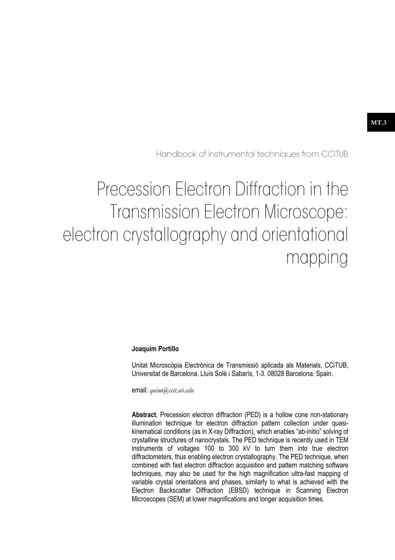
Applying this technique, a number of structures have been solved, with the same methodology used for single crystal X-ray diffraction patterns, that is, diffraction pattern indexing, intensity extraction, re-scaling of projected symmetry related intensities and phase assignation based on direct methods using programs such as SIR2008 or similar. The final output iatomic structures (number of atoms and their positions in the unit cell) with different residual values, which are taken as a reliability factor to validate the most plausible one. The residual is defined as the sum over all reflectionamplitudes and calculated diffracted amplitudes for the proposed atomic structure, see image 2 for an overview of the described process in the particular case of the mayenite mineral.
It is interesting to note in the mayenite case that a huge difference exists between the unprecessed and precessed electron diffraction patterns, as seen in figure 3. Therefore, the above described procedure would have rendered a totally wrong atomic model when applconventional electron diffraction pattern.
Precession Electron Diffraction
2
path in precessed ( or inverted hollow cone scanned) illumination of the sample, together with de-scan to produce pseudo-stationary diffracted amplitudes.
Applying this technique, a number of structures have been solved, with the same methodology ray diffraction patterns, that is, diffraction pattern indexing, intensity
scaling of projected symmetry related intensities and phase assignation based on direct methods using programs such as SIR2008 or similar. The final output is a list of proposed atomic structures (number of atoms and their positions in the unit cell) with different residual values, which are taken as a reliability factor to validate the most plausible one. The residual is defined as the sum over all reflections of the relative differences between experimental diffracted amplitudes and calculated diffracted amplitudes for the proposed atomic structure, see image 2 for an overview of the described process in the particular case of the mayenite mineral.
resting to note in the mayenite case that a huge difference exists between the unprecessed and precessed electron diffraction patterns, as seen in figure 3. Therefore, the above described procedure would have rendered a totally wrong atomic model when applconventional electron diffraction pattern.
Precession Electron Diffraction
MT.3
cessed ( or inverted hollow cone scanned) illumination of the stationary diffracted amplitudes.
Applying this technique, a number of structures have been solved, with the same methodology ray diffraction patterns, that is, diffraction pattern indexing, intensity
scaling of projected symmetry related intensities and phase assignation based on s a list of proposed
atomic structures (number of atoms and their positions in the unit cell) with different residual values, which are taken as a reliability factor to validate the most plausible one. The residual is
s of the relative differences between experimental diffracted amplitudes and calculated diffracted amplitudes for the proposed atomic structure, see image 2 for an overview of the described process in the particular case of the mayenite mineral.
resting to note in the mayenite case that a huge difference exists between the unprecessed and precessed electron diffraction patterns, as seen in figure 3. Therefore, the above described procedure would have rendered a totally wrong atomic model when applied to the

Precession Electron Diffraction
MT.3
Figure 2: PED pattern for cubic localization and list of indexed intensities. The file is used as input for SIR2008 program whichgenerates proposed atomic model, provided a rough estimate of present atomic species is given.
A digital precession instrument has been developed (called DigiSTARamong several TEM instruments, since it allows stocking in computer memory different TEMdependent alignment values for driving the beam and image coils simultaneously at different frequencies and precession angles. It is possible wcontinuously from minimum to maximum with no need to revalues, as it is the case with the analogue versions
Effectively, the most severe deformation and broadening due to several TEM aberrations, namely, spherical and threeastigmatism [4]. Thus, the beam spot size diameter is broadened by a factor of at least 3 times wthe precession angle increases to 60% of the maximum available on each particular TEM instrument, and at angles of > 2º the spot shape is no longer circular, but highly deformed. The software driving the digital version of the precession instrument enabeam shape and dimension (Fig. 4) even at high precession angles and, therefore, precessed electron diffraction patterns formed on nanocrystals may now be effectively studied under high precession angles.
3
cubic mayenite <001> , a=11.96A with corresponding spot intensity localization and list of indexed intensities. The file is used as input for SIR2008 program whichgenerates proposed atomic model, provided a rough estimate of present atomic species is given.
In this case, Ca6 Al7 O16.
A digital precession instrument has been developed (called DigiSTAR) that can be exchanged among several TEM instruments, since it allows stocking in computer memory different TEMdependent alignment values for driving the beam and image coils simultaneously at different frequencies and precession angles. It is possible with this instrument to increase precession angle continuously from minimum to maximum with no need to re-align pivot points or readjust descan values, as it is the case with the analogue versions of precession instrumentation.
Effectively, the most severe limitation imposed on the precession technique is the focused beam deformation and broadening due to several TEM aberrations, namely, spherical and three
Thus, the beam spot size diameter is broadened by a factor of at least 3 times wthe precession angle increases to 60% of the maximum available on each particular TEM instrument, and at angles of > 2º the spot shape is no longer circular, but highly deformed. The software driving the digital version of the precession instrument enables accurate correction of beam shape and dimension (Fig. 4) even at high precession angles and, therefore, precessed electron diffraction patterns formed on nanocrystals may now be effectively studied under high
with corresponding spot intensity localization and list of indexed intensities. The file is used as input for SIR2008 program which generates proposed atomic model, provided a rough estimate of present atomic species is given.
) that can be exchanged among several TEM instruments, since it allows stocking in computer memory different TEM-dependent alignment values for driving the beam and image coils simultaneously at different
ith this instrument to increase precession angle align pivot points or readjust descan
of precession instrumentation.
limitation imposed on the precession technique is the focused beam deformation and broadening due to several TEM aberrations, namely, spherical and three-fold
Thus, the beam spot size diameter is broadened by a factor of at least 3 times when the precession angle increases to 60% of the maximum available on each particular TEM instrument, and at angles of > 2º the spot shape is no longer circular, but highly deformed. The
bles accurate correction of beam shape and dimension (Fig. 4) even at high precession angles and, therefore, precessed electron diffraction patterns formed on nanocrystals may now be effectively studied under high

Figure 3: ED pattern for mayenite along Zone Axis <001>: conventional static illumination left); PED 2.4º (top right); comparison with simulated pure kinematical pattern in green
Figure 4. Digital precession unit “DigiSTAR”, shown with manual electronics (left); Deformed beam spot size at precession angle of 2º on a TEM Jeol 2000FX at 8K times magnification, diameter size 1212 nm before software correction
on-line software correction (x8000 mag
Precession Electron Diffraction
4
ttern for mayenite along Zone Axis <001>: conventional static illumination comparison with simulated pure kinematical pattern in green
Digital precession unit “DigiSTAR”, shown with manual interface and control Deformed beam spot size at precession angle of 2º on a TEM Jeol 2000FX at 8K
times magnification, diameter size 1212 nm before software correction (center); same image after line software correction (x8000 magnification, beam diameter 226nm); note a 6
the beam size (right)
Precession Electron Diffraction
MT.3
ttern for mayenite along Zone Axis <001>: conventional static illumination (top comparison with simulated pure kinematical pattern in green (bottom)
face and control
Deformed beam spot size at precession angle of 2º on a TEM Jeol 2000FX at 8K same image after
a 6-fold reduction of

Precession Electron Diffraction
5
MT.3
3.3.3.3. Precession Electron Diffraction and Orientational MappingPrecession Electron Diffraction and Orientational MappingPrecession Electron Diffraction and Orientational MappingPrecession Electron Diffraction and Orientational Mapping
Structural information from crystalline materials is present in their electron diffraction patterns, which consist of Kikuchi lines and/or individual diffraction spots. In the Precession Electron Diffraction assisted Orientational and Phase Mapping technique, collected patterns consist exclusively in spots, since Kikuchi lines are smeared out by the high frequency of the precession illumination.
Electron Backscatter Diffraction in the Scanning Electron Microscope has gained popularity over the last decade as it provides an effective tool for the characterization of bulk crystalline materials, provided lateral resolution demanded on the sample is not smaller than 500 nm [5].If a field emission gun is used in the Scanning Electron Microscope, lateral resolution may be improved down to some 50 nm, and a number of applications have been reported mainly on metals and alloys [6]. The EBSD-SEM technique is based on precise measurements of backscattered Kikuchi line diffraction patterns. However, these lines only appear after incident electron backscattering and double interaction (first inelastic scatter, then elastic diffraction) on surfaces of samples polished to mirror condition, which is a severe limitation on deformed crystalline materials. Moreover, acquisition times, although continuously improved, are still on the hour scale.
It is now possible to apply an analogue of the SEM-EBSD analysis in the TEM, by ultra-fast collection of precessed electron diffraction patterns obtained on a user-selectable area of the TEM with a point spread resolution well within the nanometer range (typically 10 nm) and without the need of additional surface sample preparation [7].
ED spot patterns are collected sequentially with an ultra-fast optical CCD camera while an area on the sample is simultaneously being scanned by the TEM focused electron beam, which is at the same time being precessed around the direction of incidence at each point. Beam scanning and precessing is controlled by a dedicated external device, which also allows control of beam pivot points and descan pivot points, called “Digistar” and manufactured by the NanoMEGAS company [8]. This device is connected to the beam and image deflector coil control boards present in the TEM. Thus, a TEM retrofitted with this precession device need not necessarily include a scanning option itself. An external ultrafast optical CCD camera, with only 8 bit dynamical range and 250 x 250 pixel image size, mounted in front of the TEM screen is used for the diffraction pattern image collection. This camera records the rapidly changing patterns appearing on the fluorescent screen of the TEM and is the key to a high collection speed since it may work as fast as 180frames/sec, although fluorescent screen reminiscence slightly slows down this performance. During the scanning and precessing of the primary electron beam, thousands of ED spot patterns are recorded and stored in memory of a dedicated computer. In order to proceed with nanocrystal orientation and/or phase identification, each one of the experimental ED spot patterns is compared to one or several sets of thousands of computer generated ED spot patterns, the so-called templates. The software technique for the comparison is based on optimal template matching using cross-correlation (Fig.4) [9].
For a typical map of 500 x 300 pixels, it may typically take only 15 minutes to scan (while precessing) over the sample area and record the associated 150.000 PED patterns. Comparison with simulated templates can be done off-line and takes about 5 minutes for highly symmetric cubic materials and 2 to 24 times longer for unit cells with lower symmetry, because more templates must be generated and compared with experimental ED spot patterns for the same angular resolution (typically 0.5 to 1º). The scanning step chosen for the rastering is about half the size of the primary electron beam size, that is 12 nm for a 25 nm spot size on a TEM with LaB6 electron gun, and the resulting lateral resolution of the obtained map will be of the order of the latter value. Template generation is done on the basis of unit cell dimensions and geometry as well as inherent atomic positions, for each of the known phases present in the examined sample. Using these data, a complete spatial set of ED spot patterns is generated under purely kinematical conditions. The comparison of these templates with experimental ED spot patterns is run, searching a maximum match for spot positions and their relative intensities, and the parameter quantifying the match is called the correlation index.

a
d
Figure 4: Schematics of PED assisted Orientational defined sample area combined with precession,
in computer memory, (c) superposition of individual ED template (red dot pattern) matches the experimental PED pattern (grey dot pattern), and (d) orientation directional map with
grey intensity plot of matching index for the
The software developed specifically for the technique allows production of crystal orientation maps, virtual bright field maps, correlation index maps and reliability index maps. The latter are related to the statistical significance of the orientational assignation chmap.
Essentially, the virtual bright fieldcentral spot in the PED pattern. Such maps are often more helpful for comparisoorientation map of the scanned area than real brightare usually suffering from diffraction contrast and curvature contrast (which fades significantly under precessed illumination). Correlatidetails such as crystals having different orientations. The reliability index, which is analogous to the SEM-EBSD confidence index, is defined in such a way that it has a minimum when more than one solution is proposed. Such reliability maps clearly reveal grain 5).
a Fig. 5 a) Orientation map revealing nanotwins in
TEM, 300KV, spot size 12 nm, step 5nmsample; (c) Reliability map showing clearly grain boundaries.
Although orientation and phase mapping coupled with template matching works satisfactorily for a number of materials without using precession of the primary electron beam, some
Precession Electron Diffraction
6
b c
assisted Orientational Mapping: (a) beam scanninge area combined with precession, (b) experimental spot PED pattern
(c) superposition of individual ED template (red dot pattern) experimental PED pattern (grey dot pattern), and (d) orientation directional map with
grey intensity plot of matching index for the experimental spot PED pattern.
The software developed specifically for the technique allows production of crystal orientation maps, virtual bright field maps, correlation index maps and reliability index maps. The latter are
nificance of the orientational assignation chosen for each point of the
ially, the virtual bright field map is obtained by plotting the intensity fluctuations of the central spot in the PED pattern. Such maps are often more helpful for comparisoorientation map of the scanned area than real bright-field TEM images of the same area, since these are usually suffering from diffraction contrast and curvature contrast (which fades significantly under precessed illumination). Correlation index maps are mainly used to emphasize structural details such as crystals having different orientations. The reliability index, which is analogous to
EBSD confidence index, is defined in such a way that it has a minimum when more than tion is proposed. Such reliability maps clearly reveal grain boundaries and textures (Fig.
b rientation map revealing nanotwins in a Cu thin foil sample (Jeol 3010 LaB6
TEM, 300KV, spot size 12 nm, step 5nm); b) Pseudo-bright field area of the same (c) Reliability map showing clearly grain boundaries.
Although orientation and phase mapping coupled with template matching works satisfactorily for a number of materials without using precession of the primary electron beam, some
Precession Electron Diffraction
MT.3
c
: (a) beam scanning over a user-(b) experimental spot PED pattern serial recording
(c) superposition of individual ED template (red dot pattern) which best experimental PED pattern (grey dot pattern), and (d) orientation directional map with
experimental spot PED pattern.
The software developed specifically for the technique allows production of crystal orientation maps, virtual bright field maps, correlation index maps and reliability index maps. The latter are
osen for each point of the
map is obtained by plotting the intensity fluctuations of the central spot in the PED pattern. Such maps are often more helpful for comparison with the final
field TEM images of the same area, since these are usually suffering from diffraction contrast and curvature contrast (which fades significantly
on index maps are mainly used to emphasize structural details such as crystals having different orientations. The reliability index, which is analogous to
EBSD confidence index, is defined in such a way that it has a minimum when more than boundaries and textures (Fig.
c Cu thin foil sample (Jeol 3010 LaB6
area of the same
Although orientation and phase mapping coupled with template matching works satisfactorily for a number of materials without using precession of the primary electron beam, some limitations
Precession Electron Diffraction
MT.3
are present in the form of ambiguous orientation/phase maps due to the poor quality of experimentally acquired ED spot patterns. This is the case for thick crystals where ED patterns show a combination of a strong diffuse inelastic scattering reduced number of faint diffraction spots. For such thick crystals and in general, precessed ED patterns exhibit a higher number of ED spots with specific intensity distribution and do not show Kikuchi lines. Consequently, the template matching software routine will produce higher values of the correlation index when using PED patterns and orientation maps will exhibit less ambiguity[10].
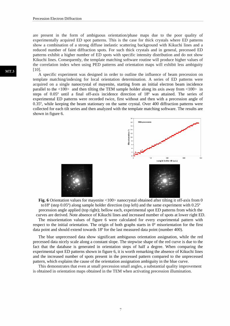
A specific experiment was designed in order to outline the influence of beam precetemplate matching/indexing for local orientation determination. A series of ED patterns were acquired on a single nanocrystal of mayenite, starting from an initial electron beam incidence parallel to the <100> and then tilting the TEM sample holdsteps of 0.05º until a final offexperimental ED patterns were recorded twice, first without and then with a precession angle of 0.35º, while keeping the beamcollected for each tilt series and then analyzed with the template matching software. Theshown in figure 6.
Fig. 6 Orientation values for mayeniteto18º (step 0.05º) along sample holder direction (top left) and
precession angle applied (top right); bellow each, curves are derived. Note absence of Kikuchi lineThe misorientation values of figure 6 were calculated for every experimental pattern with
respect to the initial orientation. The origin of both graphs starts in 0º misorientatidata point and should extend towards 18º for the last measured data point (numbe
The blue unprecessed data show significant ambiguous orientation assignation, while the red precessed data nicely scale along a constant slope. The stepwise shape of the red curve is due to the fact that the database is generated in orientation steps of half a degree. When comparing the experimental spot ED patterns shown in figure 6, it is worth remarkinand the increased number of spots present in the precessed pattern compared to the unprecessed pattern, which explains the cause of the orientation assignati
This demonstrates that even at smallis obtained in orientation maps obtained in the TEM when activating precession illumination.
7
are present in the form of ambiguous orientation/phase maps due to the poor quality of experimentally acquired ED spot patterns. This is the case for thick crystals where ED patterns show a combination of a strong diffuse inelastic scattering background with Kikuchi lines and a reduced number of faint diffraction spots. For such thick crystals and in general, precessed ED patterns exhibit a higher number of ED spots with specific intensity distribution and do not show
y, the template matching software routine will produce higher values of the correlation index when using PED patterns and orientation maps will exhibit less ambiguity
A specific experiment was designed in order to outline the influence of beam precetemplate matching/indexing for local orientation determination. A series of ED patterns were
nanocrystal of mayenite, starting from an initial electron beam incidence parallel to the <100> and then tilting the TEM sample holder along its axis away from <100> in steps of 0.05º until a final off-axis incidence direction of 18º was attained. The series of experimental ED patterns were recorded twice, first without and then with a precession angle of 0.35º, while keeping the beam stationary on the same crystal. Over 400 diffraction patterns were collected for each tilt series and then analyzed with the template matching software. The
ntation values for mayenite <100> nanocrystal obtained after tilting it off
) along sample holder direction (top left) and the same experiment with 0.25º applied (top right); bellow each, experimental spot ED pattern
ote absence of Kikuchi lines and increased number of spots at lower right ED.The misorientation values of figure 6 were calculated for every experimental pattern with
respect to the initial orientation. The origin of both graphs starts in 0º misorientatidata point and should extend towards 18º for the last measured data point (numbe
The blue unprecessed data show significant ambiguous orientation assignation, while the red data nicely scale along a constant slope. The stepwise shape of the red curve is due to the
fact that the database is generated in orientation steps of half a degree. When comparing the experimental spot ED patterns shown in figure 6, it is worth remarking the absence of Kikuchi lines and the increased number of spots present in the precessed pattern compared to the unprecessed pattern, which explains the cause of the orientation assignation ambiguity in the blue curve.
This demonstrates that even at small precession small angles, a substantial quality improvement is obtained in orientation maps obtained in the TEM when activating precession illumination.
are present in the form of ambiguous orientation/phase maps due to the poor quality of experimentally acquired ED spot patterns. This is the case for thick crystals where ED patterns
background with Kikuchi lines and a reduced number of faint diffraction spots. For such thick crystals and in general, precessed ED patterns exhibit a higher number of ED spots with specific intensity distribution and do not show
y, the template matching software routine will produce higher values of the correlation index when using PED patterns and orientation maps will exhibit less ambiguity
A specific experiment was designed in order to outline the influence of beam precession on template matching/indexing for local orientation determination. A series of ED patterns were
nanocrystal of mayenite, starting from an initial electron beam incidence er along its axis away from <100> in
axis incidence direction of 18º was attained. The series of experimental ED patterns were recorded twice, first without and then with a precession angle of
stationary on the same crystal. Over 400 diffraction patterns were collected for each tilt series and then analyzed with the template matching software. The results are
ained after tilting it off-axis from 0
the same experiment with 0.25º experimental spot ED patterns from which the
s and increased number of spots at lower right ED. The misorientation values of figure 6 were calculated for every experimental pattern with
respect to the initial orientation. The origin of both graphs starts in 0º misorientation for the first data point and should extend towards 18º for the last measured data point (number 400).
The blue unprecessed data show significant ambiguous orientation assignation, while the red data nicely scale along a constant slope. The stepwise shape of the red curve is due to the
fact that the database is generated in orientation steps of half a degree. When comparing the g the absence of Kikuchi lines
and the increased number of spots present in the precessed pattern compared to the unprecessed on ambiguity in the blue curve.
precession small angles, a substantial quality improvement is obtained in orientation maps obtained in the TEM when activating precession illumination.

Precession Electron Diffraction
8
MT.3
A B
C
Fig. 7 (a) Orientation mapping of mayenite crystals without precession; (b) Virtual bright field; (c) Orientation map obtained with precession angle of 0.35º
This clear improvement of orientation determination can also be shown in the maps of Fig. 7 where an area that contains randomly oriented mayenite crystals was scanned twice (with and without precession). The orientation map in Fig. 7a shows color fluctuations indicating frequent misassigned patterns because of their low quality when compared with simulated templates. The map in Fig. 7c was obtained under the same conditions as in Fig.7a but using precession at 0.35º angle during beam scanning. As it can be observed, orientation map quality increases with precession, since each color domain corresponds to a single crystal grain with a definite orientation and should not show color fluctuations, as it is the case.
AcknowledgAcknowledgAcknowledgAcknowledgmentsmentsmentsments
Samples for Figure 5 were supplied by Prof. Nuria Llorca of the University of Barcelona. The author is also indebted to Dr. Francesca Peiró of the University of Barcelona for fruitful discussions, encouragement and willing collaboration on Precession related topics.
ReferencesReferencesReferencesReferences
[1] T.E.Weirich, J.Portillo, G.Cox, H.Hibst, S.Nicolopoulos, “Ab initio determination of framework structure of CsNbWO from 100KV precession data”, Ultramicroscopy 106 (2007), 164-175 [2] A.Avilov, K.Kuligin, S.Nicolopoulos, M.Nickolsky, K.Boulahya, J.Portillo, G.Lepeshov, B.Sobolev, J.P.Collette, N.Martin, A.C.Robins, P.Fischione, “Precession technique and electron diffractometry as new tools for crystal structure and chemical bonding”, Ultramicroscopy 107 (2007), 431-444 [3] E.F.Rauch, M.Veron, J.Portillo, D.Bultreys, Y.Maniette, S.Nicolopoulos, “Automatic crystal orientation and phase mapping in TEM by precession diffraction”, Microsc. Anal. 93 (2008), 5-8 [4] C. Own, PhD dissertation, Northwestern University, Chicago, December 2004, http://www.numis.northwestern.edu/Research/Current/precession [5] V.Randle, O.Engler, “Introduction to texture Analysis: Macrotexture, Microtexture and Orientation Mapping”, CRC Press, 2000 [6] D.P.Field, S.I.Wright, D.J.Dingley, Proc. 11th International Conference on Textures of Materials (ICOTOM11), Ed. Z. Liang et al, International Academic Publishers, China, 1994 [7] E.F.Rauch, M.Veron, “Coupled microstructural observations of local texture measurements with an automated crystallographic orientation mapping tool attached to a TEM”, J.Mater.Sci. Eng. Tech. 36 (2005), 552-556 [8] http://www.nanomegas.com, NanoMEGAS-CNRS Patent pending technique [9] E.F. Rauch, L. Dupuy, “Rapid spot diffraction pattern identification through template matching”, Arch. Metall. Mater 50 (2005), 87-99. [10] J.Portillo, E.F.Rauch, S.Nicolopoulos, M.Gemmi, D.Bultreys, “Precession Electron Diffraction assisted Orientation Mapping in the Transmission Electron Microscope”, Mat. Sci. Forum 644 (2010), 1-7

Precession Electron Diffraction
9
MT.3