Embed Size (px)
Citation preview
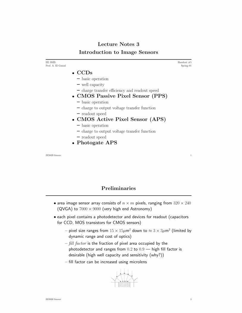
Lecture Notes 3
Introduction to Image Sensors
EE 392B Handout #5
Prof. A. El Gamal Spring 01
• CCDs– basic operation
– well capacity
– charge transfer efficiency and readout speed
• CMOS Passive Pixel Sensor (PPS)– basic operation
– charge to output voltage transfer function
– readout speed
• CMOS Active Pixel Sensor (APS)– basic operation
– charge to output voltage transfer function
– readout speed
• Photogate APS
EE392B Sensors 1
Preliminaries
• area image sensor array consists of n × m pixels, ranging from 320 × 240
(QVGA) to 7000 × 9000 (very high end Astronomy)
• each pixel contains a photodetector and devices for readout (capacitors
for CCD, MOS transistors for CMOS sensors)
– pixel size ranges from 15 × 15µm2 down to ≈ 3 × 3µm2 (limited by
dynamic range and cost of optics)
– fill factor is the fraction of pixel area occupied by the
photodetector and ranges from 0.2 to 0.9 — high fill factor is
desirable (high well capacity and sensitivity (why?))
– fill factor can be increased using microlens
EE392B Sensors 2
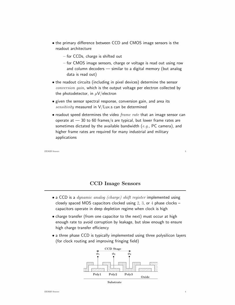
• the primary difference between CCD and CMOS image sensors is the
readout architecture
– for CCDs, charge is shifted out
– for CMOS image sensors, charge or voltage is read out using row
and column decoders — similar to a digital memory (but analog
data is read out)
• the readout circuits (including in pixel devices) determine the sensor
conversion gain, which is the output voltage per electron collected by
the photodetector, in µV/electron
• given the sensor spectral response, conversion gain, and area its
sensitivity measured in V/Lux.s can be determined
• readout speed determines the video frame rate that an image sensor can
operate at — 30 to 60 frames/s are typical, but lower frame rates are
sometimes dictated by the available bandwidth (e.g., PC camera), and
higher frame rates are required for many industrial and military
applications
EE392B Sensors 3
CCD Image Sensors
• a CCD is a dynamic analog (charge) shift register implemented using
closely spaced MOS capacitors clocked using 2, 3, or 4 phase clocks –
capacitors operate in deep depletion regime when clock is high
• charge transfer (from one capacitor to the next) must occur at high
enough rate to avoid corruption by leakage, but slow enough to ensure
high charge transfer efficiency
• a three phase CCD is typically implemented using three polysilicon layers
(for clock routing and improving fringing field)
Poly1 Poly2 Poly3
φ1 φ2 φ3
CCD Stage
Oxide
Substrate
EE392B Sensors 4
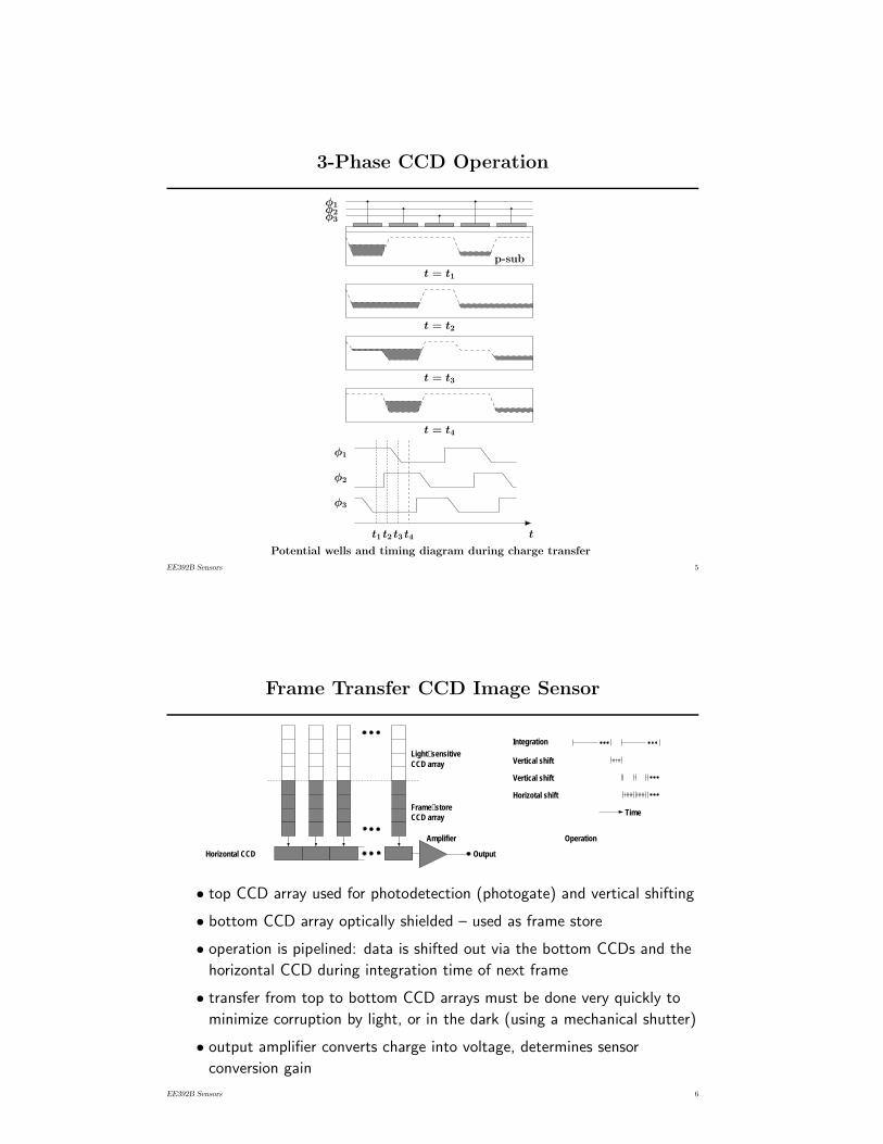
3-Phase CCD Operation
φ1
φ1
φ2
φ2
φ3
φ3
t = t1
t = t2
t = t3
t = t4
t1 t2 t3 t4 t
p-sub
Potential wells and timing diagram during charge transfer
EE392B Sensors 5
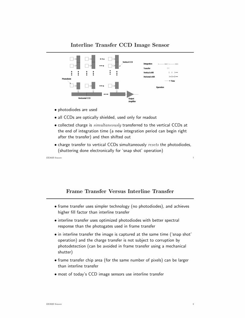
Frame Transfer CCD Image Sensor
Frame−storeCCD array
CCD array Vertical shift
Vertical shift
Integration
Horizotal shift
Time
Operation
Output
Amplifier
Light−sensitive
Horizontal CCD
• top CCD array used for photodetection (photogate) and vertical shifting
• bottom CCD array optically shielded – used as frame store
• operation is pipelined: data is shifted out via the bottom CCDs and the
horizontal CCD during integration time of next frame
• transfer from top to bottom CCD arrays must be done very quickly to
minimize corruption by light, or in the dark (using a mechanical shutter)
• output amplifier converts charge into voltage, determines sensor
conversion gain
EE392B Sensors 6
Interline Transfer CCD Image Sensor
Vertical shift
Integration
Horizotal shift
Time
Operation
Transfer
OutputAmplifier
Horizontal CCD
Vertical CCD
Photodiode
• photodiodes are used
• all CCDs are optically shielded, used only for readout
• collected charge is simultaneously transferred to the vertical CCDs at
the end of integration time (a new integration period can begin right
after the transfer) and then shifted out
• charge transfer to vertical CCDs simultaneously resets the photodiodes,
(shuttering done electronically for ‘snap shot’ operation)
EE392B Sensors 7
Frame Transfer Versus Interline Transfer
• frame transfer uses simpler technology (no photodiodes), and achieves
higher fill factor than interline transfer
• interline transfer uses optimized photodiodes with better spectral
response than the photogates used in frame transfer
• in interline transfer the image is captured at the same time (‘snap shot’
operation) and the charge transfer is not subject to corruption by
photodetection (can be avoided in frame transfer using a mechanical
shutter)
• frame transfer chip area (for the same number of pixels) can be larger
than interline transfer
• most of today’s CCD image sensors use interline transfer
EE392B Sensors 8
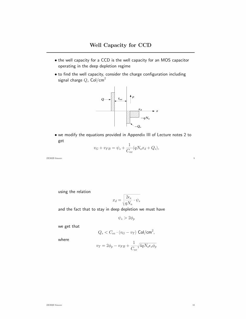
Well Capacity for CCD
• the well capacity for a CCD is the well capacity for an MOS capacitor
operating in the deep depletion regime
• to find the well capacity, consider the charge configuration including
signal charge Qs Col/cm2
ρ
xxd
tox
−qNa
Q
−Qs
• we modify the equations provided in Appendix III of Lecture notes 2 to
get
vG + vFB = ψs +1
Cox(qNaxd + Qs),
EE392B Sensors 9
using the relation
xd =
√√√√√√√2εs
qNa· ψs
and the fact that to stay in deep depletion we must have
ψs > 2φp
we get that
Qs < Cox · (vG − vT ) Col/cm2,
where
vT = 2φp − vFB +1
Cox
√4qNaεsφp
EE392B Sensors 10
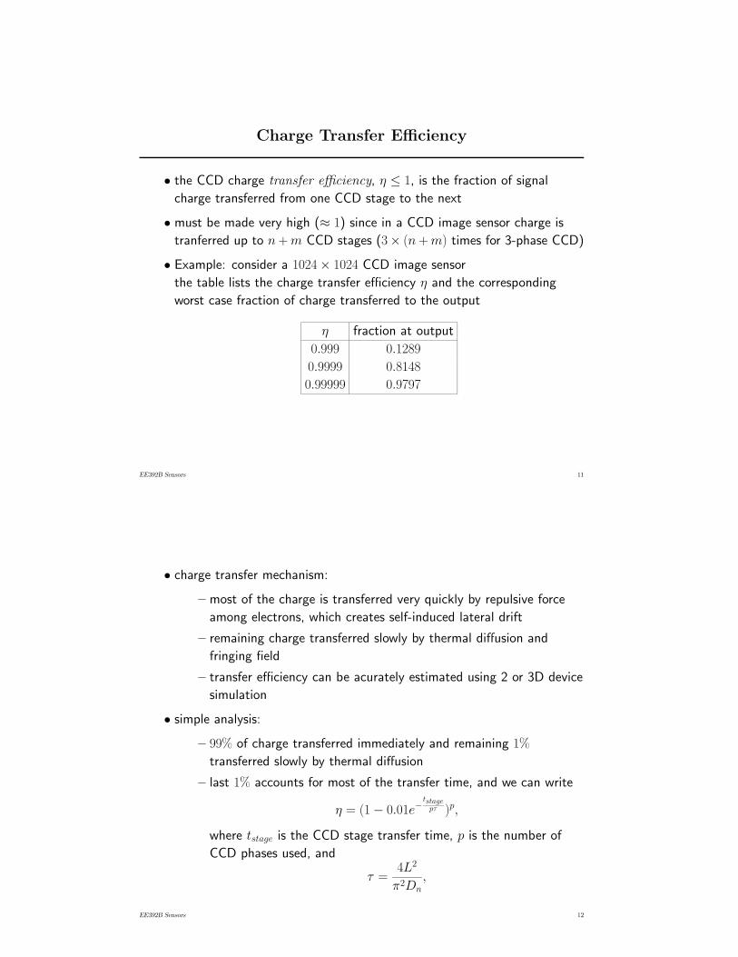
Charge Transfer Efficiency
• the CCD charge transfer efficiency, η ≤ 1, is the fraction of signal
charge transferred from one CCD stage to the next
• must be made very high (≈ 1) since in a CCD image sensor charge is
tranferred up to n + m CCD stages (3× (n + m) times for 3-phase CCD)
• Example: consider a 1024 × 1024 CCD image sensor
the table lists the charge transfer efficiency η and the corresponding
worst case fraction of charge transferred to the output
η fraction at output
0.999 0.1289
0.9999 0.8148
0.99999 0.9797
EE392B Sensors 11
• charge transfer mechanism:
– most of the charge is transferred very quickly by repulsive force
among electrons, which creates self-induced lateral drift
– remaining charge transferred slowly by thermal diffusion and
fringing field
– transfer efficiency can be acurately estimated using 2 or 3D device
simulation
• simple analysis:
– 99% of charge transferred immediately and remaining 1%
transferred slowly by thermal diffusion
– last 1% accounts for most of the transfer time, and we can write
η = (1 − 0.01e−tstage
pτ )p,
where tstage is the CCD stage transfer time, p is the number of
CCD phases used, and
τ =4L2
π2Dn,
EE392B Sensors 12
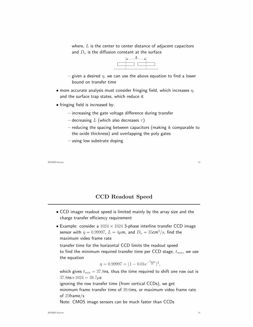
where, L is the center to center distance of adjacent capacitors
and Dn is the diffusion constant at the surfaceL
– given a desired η, we can use the above equation to find a lower
bound on transfer time
• more accurate analysis must consider fringing field, which increases η,
and the surface trap states, which reduce it
• fringing field is increased by:
– increasing the gate voltage difference during transfer
– decreasing L (which also decreases τ)
– reducing the spacing between capacitors (making it comparable to
the oxide thickness) and overlapping the poly gates
– using low substrate doping
EE392B Sensors 13
CCD Readout Speed
• CCD imager readout speed is limited mainly by the array size and the
charge transfer efficiency requirement
• Example: consider a 1024 × 1024 3-phase interline transfer CCD image
sensor with η = 0.99997, L = 4µm, and Dn = 35cm2/s, find the
maximum video frame rate
transfer time for the horizontal CCD limits the readout speed
to find the minimum required transfer time per CCD stage, tmin, we use
the equation
η = 0.99997 = (1 − 0.01e−tmin3τ )3,
which gives tmin = 37.8ns, thus the time required to shift one row out is
37.8ns×1024 = 38.7µs
ignoring the row transfer time (from vertical CCDs), we get
minimum frame transfer time of 39.6ms, or maximum video frame rate
of 25frame/s
Note: CMOS image sensors can be much faster than CCDs
EE392B Sensors 14
Advantages and Disadvantages of CCDs
• Advantages: high quality
– optimized photodetectors — high QE, low dark current
– very low noise — no noise introduced during shifting
– very low fixed pattern noise (nonuniformity) — no FPN
introduced by shifting
• Disadvantages:
– cannot integrate other analog or digital circuits, e.g., for clock
generation, control, or A/D conversion
– highly nonprogrammable, e.g., difficult to implement window of
interest
– high power — entire array switching all the time (high C, high V ,
and high f result in high CV 2f)
– limited frame rate (for large sensors) due to required increase in
transfer speed (while maintaining acceptable transfer efficiency)
EE392B Sensors 15
CMOS Passive and Active Pixel Sensors
treansistors
Output
Bit
Word
Row
Dec
oder
PhotodetectorPixel:
& Readout
Column Amplifiers/Caps
Column Mux
• readout done by transferring one row at a time to the column storage
capacitors, then reading out the row one (or more) pixel at a time using
the column decoder and multiplexer
• row integration times are staggerred by the row/column readout time,
‘snap shot’ operation can be achieved using a mechanical shutter
EE392B Sensors 16
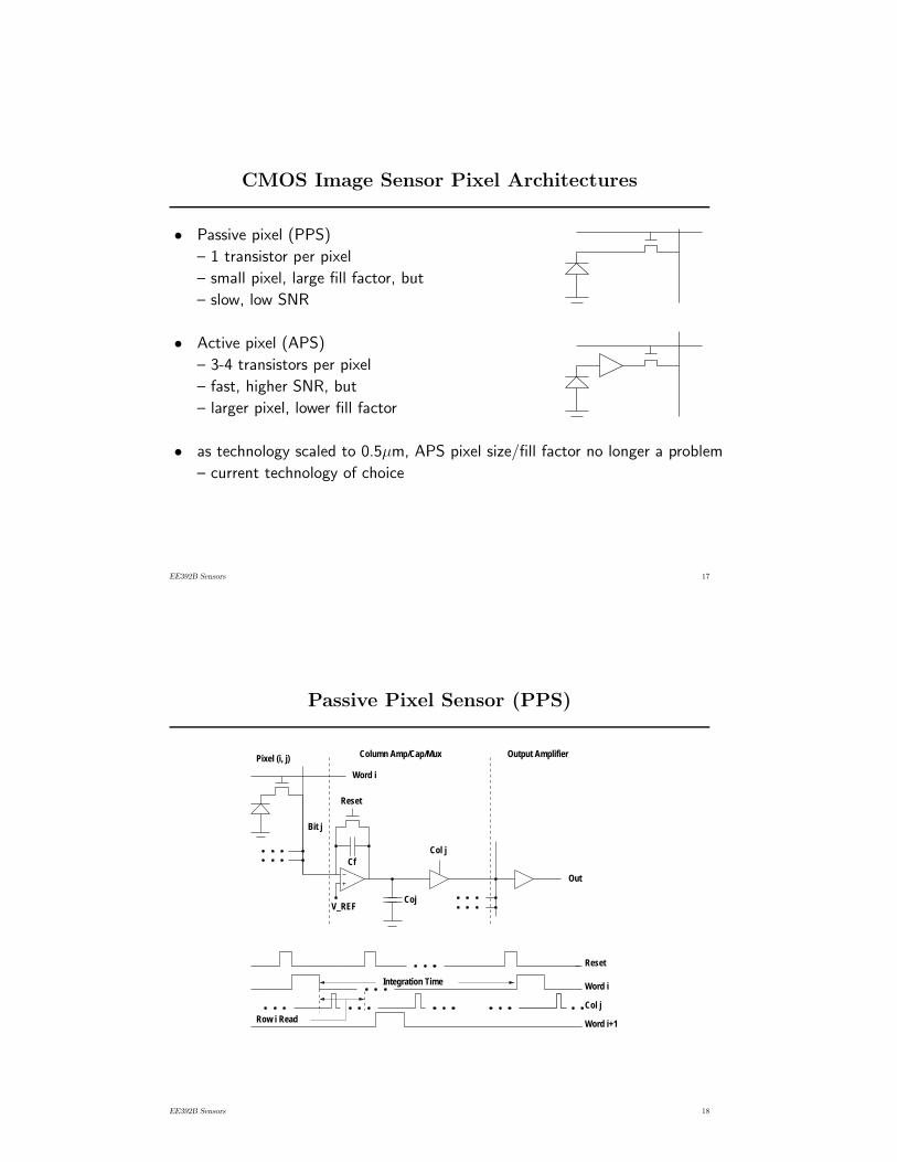
CMOS Image Sensor Pixel Architectures
• Passive pixel (PPS)
– 1 transistor per pixel
– small pixel, large fill factor, but
– slow, low SNR
• Active pixel (APS)
– 3-4 transistors per pixel
– fast, higher SNR, but
– larger pixel, lower fill factor
• as technology scaled to 0.5µm, APS pixel size/fill factor no longer a problem
– current technology of choice
EE392B Sensors 17
Passive Pixel Sensor (PPS)
Cf
Coj
Word iIntegration Time
Col j
Word i+1Row i Read
Pixel (i, j)
Out
Output Amplifier
Col j
Word i
Bit j
V_REF
Column Amp/Cap/Mux
Reset
Reset
EE392B Sensors 18
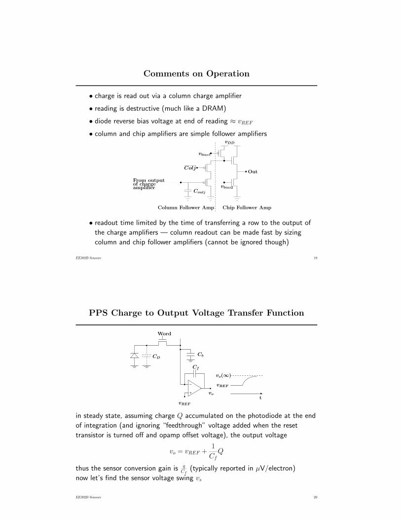
Comments on Operation
• charge is read out via a column charge amplifier
• reading is destructive (much like a DRAM)
• diode reverse bias voltage at end of reading ≈ vREF
• column and chip amplifiers are simple follower amplifiersvDD
vbias1
ColjOut
vbias2Coutj
Chip Follower AmpColumn Follower Amp
From outputof chargeamplifier
• readout time limited by the time of transferring a row to the output of
the charge amplifiers — column readout can be made fast by sizing
column and chip follower amplifiers (cannot be ignored though)
EE392B Sensors 19
PPS Charge to Output Voltage Transfer Function
Word
CDCb
Cf
vREF
vREF
vo
vo(∞)
t
in steady state, assuming charge Q accumulated on the photodiode at the end
of integration (and ignoring “feedthrough” voltage added when the reset
transistor is turned off and opamp offset voltage), the output voltage
vo = vREF +1
CfQ
thus the sensor conversion gain is qCf
(typically reported in µV/electron)
now let’s find the sensor voltage swing vs
EE392B Sensors 20
the minimum output voltage occurs when Q = 0, ignoring dark current we get
vomin = vREF
the maximum output voltage occurs when the voltage on the diode reaches
ground, which gives
vomax = vREF +CD
CfvREF ,
provided that vomax does not exceed the opamp maximum output voltage vSat
(in this case vomax = vSat)
thus the sensor voltage swing
vs = min{CD
CfvREF , vSat − vREF}
Note: since the column amplifier, which can be made quite linear, is used to
convert the collected charge to voltage, the output voltage is linear in
illumination (F0), this is similar to CCDs (but different from APS as we shall
see)
Special case for examples: we assume Cf = CD, which gives
vs = min{vREF , vSat − vREF}
EE392B Sensors 21
PPS Readout Speed
• row readout is done in two stages; first the row is transferred to the
column capacitors, then the column decoder/multiplexer is used to
serially read out the pixel values
• row transfer time can be the dominant readout time
• row transfer time is the time from Word going high to the time vo is
within ε of its final value (vo(∞))
• for k bits of resolution choose
ε ≤ vs
2 × 2kV,
where vs is the output voltage swing, e.g., for k = 8 bits,
ε ≤ vs
512
• worst transfer time occurs when vo(∞) is maximum, i.e., equal to vomax
• Example: consider a PPS with n = 256 rows, CD = Cf = 20fF, and
Cb = n × 2.6fF= 0.6656pF, find the maximum row transfer time
assuming k = 8 bits of resolution
EE392B Sensors 22

to simplify the analysis we assume:
– single-pole open-loop model for the opamp used in the charge
amplifierVo(s)
V+(s) − V−(s)= A(s) =
A
1 + ( sωo
)
with dc gain A = 6 × 10⁴ and 3dB bandwidth ωo = 100rad/s
– access transistor has negligible ON resistance
to find the row transfer time, we assume that the charge sharing
between CD and Cb occurs instantaneously (the access transistor treated
as a short circuit) and use the equivalent circuit
vo(t)
Cb + CD
Cf
vREF
t = 0
EE392B Sensors 23
to find the transfer time we substitute the single-pole opamp model to
get
Vi(s)
Cb + CD Cf
Vo(s)
−A(s) · V−(s)+
−
the transfer function
Vo(s)
Vi(s)≈ −Cb + CD
Cf· 1
1 + s
(AωoCf
Cb+CD+Cf)
thus the time constant
τ =Cb + CD + Cf
AωoCf= 5.88µs,
and
worst case row transfer time = τ ln(256 × 2) = 36.5µs
EE392B Sensors 24

• note that
– row transfer time increases almost linearly with Cb (and the
number of rows)
– readout time can be reduced by increasing the gain-bandwidth
product of the opamp (Aωo), which would increase power
consumption
EE392B Sensors 25
Active Pixel Sensor (APS)
Bit j
Word i
Reset i
Pixel (i,j)
Col j
Output Amplifier Column Amp/Cap/Mux
Integration TimeReset i
Word i
Col j
Word i+1
Reset i+1
Row i Read
Vbias Coj
Out
EE392B Sensors 26
Comments on Operation
• direct integration is used, voltage is read out of the pixel
• output of the photodiode is “buffered” using pixel level follower amplifier
— reading is not destructive and can be much faster than PPS
• each row has separate reset (used after reading)
• the photodiode reset voltage vD = vDD − vTR, where vTR is the reset
transistor threshold voltage (including body effect)
• by setting the voltage on the reset gate vReset ≥ vTR (instead of ground)
during integration, blooming can be controlled (reset transistor doubles
as anti-blooming device)
• except for eliminating the charge amplifier, the column amplifier and
decoder are identical to PPS
EE392B Sensors 27
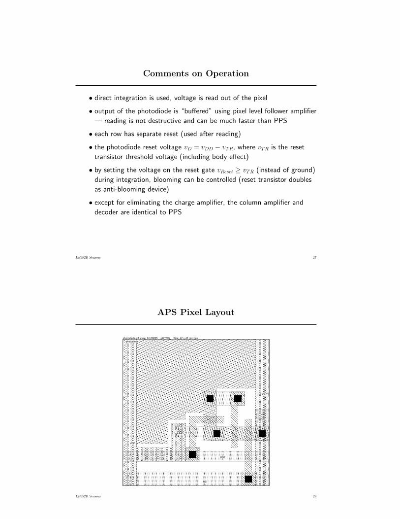
APS Pixel Layout
photodiode.cif scale: 0.188095 (4778X) Size: 42 x 42 microns
���������������������������������������������������������������������������������������������������������������������������������������������������
����������������������������������������������������������������
������������������������������������������������������������
������������������������������������������������������������������������������������
��������������������������������������������������������������������������������
���������������������������������
������
��������������������
���
������������
������������������������
���
������
����������������������������
���
���������������������������������������
���������
������������
������������������
������������
���������������������������
������������������������������������������������������������������������������������������
���������������������������������������������
����������������������������
������������������������������������������������������������������������������������������
������������������������
������������������������
������������������������������������������������������������������������������������������������������������������������
photodiode
OUT
VDD
RST
RS
EE392B Sensors 28
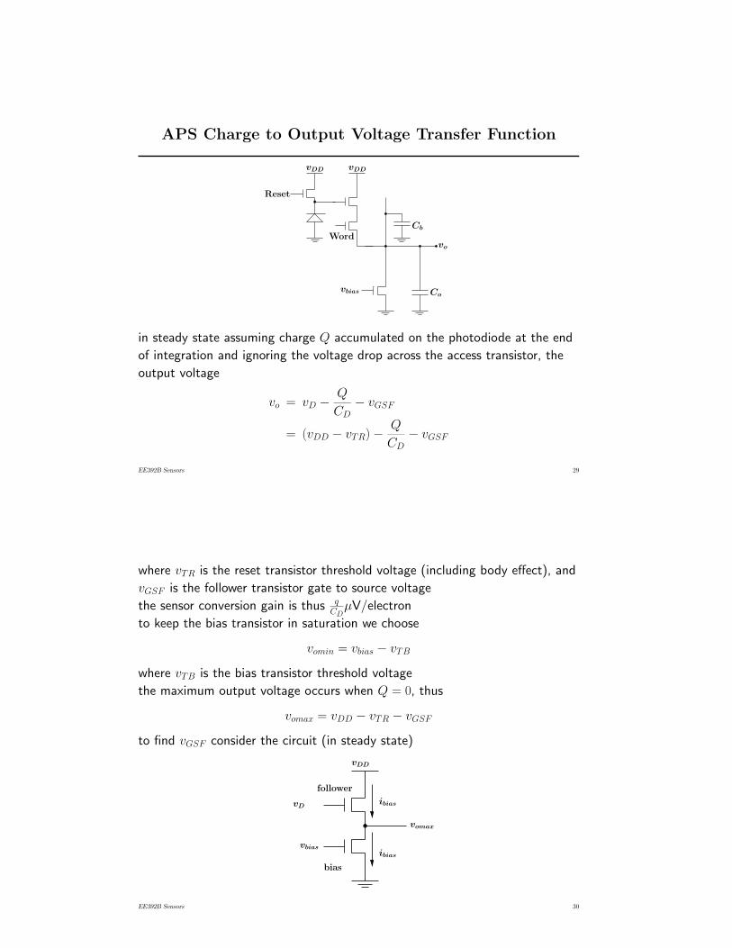
APS Charge to Output Voltage Transfer Function
WordCb
Covbias
Reset
vDDvDD
vo
in steady state assuming charge Q accumulated on the photodiode at the end
of integration and ignoring the voltage drop across the access transistor, the
output voltage
vo = vD − Q
CD− vGSF
= (vDD − vTR) − Q
CD− vGSF
EE392B Sensors 29
where vTR is the reset transistor threshold voltage (including body effect), and
vGSF is the follower transistor gate to source voltage
the sensor conversion gain is thus qCD
µV/electron
to keep the bias transistor in saturation we choose
vomin = vbias − vTB
where vTB is the bias transistor threshold voltage
the maximum output voltage occurs when Q = 0, thus
vomax = vDD − vTR − vGSF
to find vGSF consider the circuit (in steady state)
vDD
vD
vbias
ibias
ibias
vomax
follower
bias
EE392B Sensors 30

where ibias is the column amplifier bias current
assuming the static first order MOS transistor model, we get
ibias =kn
2· WF
LF(vGSF − vTF )2
where WF and LF are the follower transistor width and length, and vTF is its
threshold voltage
thus we get that
vGSF = vTF +
√√√√√√√2LF
knWFibias
thus the voltage swing is given by
vs = vDD − vTR − vGSF − vbias + vTB
Remarks:
• the available well capacity Qmax = vD × CD cannot be fully utilized,
since vomin is achieved before the diode voltage drops to ground
• since the collected charge is converted to voltage using the diode
capacitance CD, the output voltage can be somewhat nonlinear in
illumination (F0)
EE392B Sensors 31
APS Readout Speed
• readout time for a row is the sum of the time to transfer the row to the
column capacitors and the time to read out the pixel values via the
column multiplexer (column readout time)
• unlike for PPS, APS column readout time (and not row transfer time) is
the real performance limiter
• Example: consider an APS implemented in the 0.5µ CMOS technology
described in Handout 2 with n = 256 rows, vTF = 0.9V, vTR = 1.1V,
vTB = 0.8V, and the parameters shown in the figure
EE392B Sensors 32

WordCb = n × 3fF
Co = 3pF1V16/32
4/2
4/24/2
Reset
3.3V3.3V
vo
find the row transfer time assuming k = 8 bits of resolution
first let’s compute the output voltage swing vs
the minimum output voltage
vomin = vbias − vTB = 0.2V
the bias current using kn = 188µA/V2
ibias = 1.88µA
thus the maximum output voltage
vomax = vDD − vTR − vGSF = 3.3 − 1.1 − 1.0 = 1.2V,
EE392B Sensors 33
and
vs = 1.0V
to find the worst case row transfer time, we use the equivalent circuit
3.3V
3.3V
2.2V
0V
1.88µA
vo
C′o = (3 + 0.768)pF
follower
from KCL
1.88 × 10⁻⁶ + C ′o ·
dvo
dt= 188 × 10−6 × (1.3 − vo)
2
now we solve the differential equation to find the row transfer time trow
∫ trow0 dt = trow = C ′
o
∫ 1.1980.2
dvo × 106
188(1.3 − vo)2 − 1.88
EE392B Sensors 34
=106 × C ′
o
188
∫ 1.1980.2
dvo
(1.3 − vo)2 − 10−2
=106 × C ′
o
188 × 0.2
∫ 1.1980.2 (
1
1.2 − vo− 1
1.4 − vo)dvo
=3.768 × 10⁻⁶
188 × 0.2× 4.43
= 444ns
where the lower limit of the integral is vomin and the upper limit is
(vomax − vs512)
• note that
– the row transfer time increases linearly in Cb (same as PPS)
– it is considerably faster than PPS (our estimate is, however,
somewhat optimistic as you can see from the HSPICE simulations)
– PPS can be made as fast using a fast charge amplifier, but power
consumption would be much higher than APS
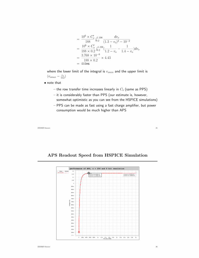
EE392B Sensors 35
APS Readout Speed from HSPICE Simulation
SymbolWaveD0:A0:v(bit)
Vol
tage
s (li
n)
150m
200m
250m
300m
350m
400m
450m
500m
550m
600m
650m
700m
750m
800m
850m
900m
950m
1
1.05
1.1
1.15
1.2
Time (lin) (TIME)0 200n 400n 600n 800n 1u 1.2u 1.4u 1.6u 1.8u 2u 2.2u 2.4u 2.6u 2.8u 3u
Current Y=1.1605e+00Current X=3.0000e-06
Current Y=1.1586e+00Current X=5.2835e-07
performance of APS, n = 256 and 8 bit resolution
EE392B Sensors 36
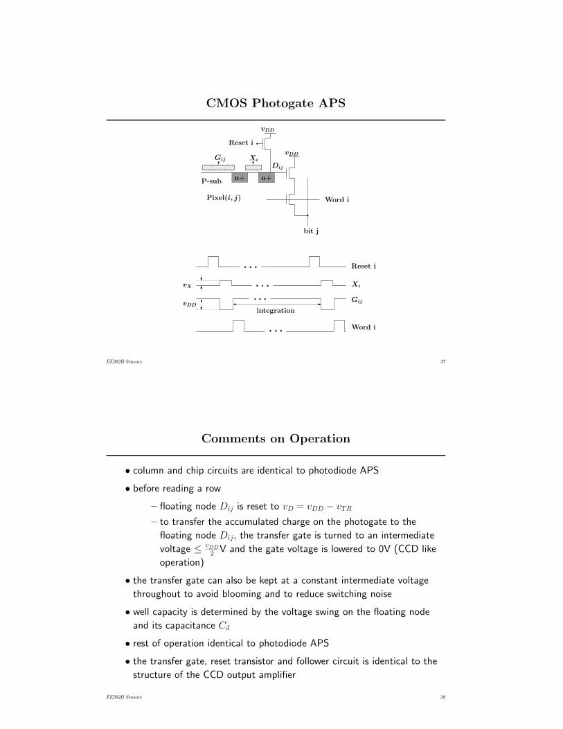
CMOS Photogate APS
vDD
vDD
vDD
vX
Reset i
Reset i
Xi
Xi
Pixel(i, j)
P-sub
Dij
n+n+
Word i
Word i
bit j
Gij
Gij
integration
EE392B Sensors 37
Comments on Operation
• column and chip circuits are identical to photodiode APS
• before reading a row
– floating node Dij is reset to vD = vDD − vTR
– to transfer the accumulated charge on the photogate to the
floating node Dij, the transfer gate is turned to an intermediate
voltage ≤ vDD2 V and the gate voltage is lowered to 0V (CCD like
operation)
• the transfer gate can also be kept at a constant intermediate voltage
throughout to avoid blooming and to reduce switching noise
• well capacity is determined by the voltage swing on the floating node
and its capacitance Cd
• rest of operation identical to photodiode APS
• the transfer gate, reset transistor and follower circuit is identical to the
structure of the CCD output amplifier
EE392B Sensors 38
Potential Well Diagram for Photogate APS
G X
vDD
Reset
During integration
During reset
During charge transfer
During readout
EE392B Sensors 39
Photogate APS Pixel Layout
photogate.cif scale: 0.168085 (4269X) Size: 47 x 47 microns
������������������������������������������������������������
������������������������������������������
���������������������
���������������������������������
������������������������������������������������������������������������
������������
������������������������������
�������������������������������������������������������������������������������������������������������������������������������������������������������������������������������������������
������������������������������������������������������������������������������������������������������������������������������
��������������
����������������
������������
��������
������������������������������������������������
��������
������������
��������
��������������������������
������
��������������
���
����������������������������������������������
��������������
����������������
��������
����
��������
����
����������������������������
������������
������������
������������
��
��
������������������������������������������������������������������������������������������������������������������������������������������������������������������������������������������������������������������������������������������������������������������������������������������������������
������������
���������������������
������������������
������������������������������
���������������
���������������������������
������������������������������
������������������������������������������������������������������������������������������
������������������������������������������������������������������������������������������
photogate
RS
Ttx
out
reset
Vdd
Tpg
EE392B Sensors 40
Advantages and Disadvantages of Photogate
• advantages
– conversion gain qCd
is independent of detector, can achieve higher
conversion gain than photodiode APS (lower QE, however)
– Cd very useful when performing correlated double sampling (CDS)
(as we will see later) and may be used to perform frame
differencing (read-reset-read new frame)
• disadvantages
– more devices (larger pixel or lower fill factor than photodiode)
– poor blue response
EE392B Sensors 41


![[Tutorial] CMOS Image Sensors.pdf](https://img.pdfslide.net/doc/110x75/55cf9c66550346d033a9b510/tutorial-cmos-image-sensorspdf.jpg)