Embed Size (px)
Citation preview

Part Number
Data Sheet - Chapter
www.austriamicrosystems.com/AS5410
Revision 1.5 1 - 28
Preliminary Data Sheet
1 General Description The chip can measure magnetic fields components in
all three dimensions and converts the magnetic field
information into absolute, position information. The
AS5410 supports absolute linear position
measurement applications.
Only a simple 2-pole magnet is required as the
magnetic field source.
Using two 3D-Hall cells allows both absolute as well
as differential 3D magnetic field measurement.
The differential measurement makes the AS5410
ideal for use in rough industrial position sensing
applications that include not only dust, dirt or
moisture but also unwanted magnetic fields.
All the signal conditioning, including compensation of
temperature effects, magnet-to-chip gap changes as
well as linearization of the output is included in the
IC.
The absolute position information of the magnet is
directly accessible over a SPI interface and PWM
output. A cycle redundancy check (CRC) allows
verification of the received data.
The AS5410 is available in a 14-pin TSSOP package
and is qualified for an ambient temperature range
from -40°C to +105°C.
It operates at a supply voltage of 3.3V +/-10%.
2 Key Features � up to 14-bit full scale resolution
� SPI and PWM output
� Wide magnetic input range
� 33 linearization points to achieve high precision
� Absolute linear position sensing up to 50 mm
stroke
� Suppression of magnetic stray fields
� Low power operation
3 Applications
� Plunger positioning
� Pedal positioning
� Pneumatic and hydraulic cylinder positioning
� Automation with linear positioning stages through
cascading of several AS5410’s
AS5410 3D-Hall Encoder absolute linear
Figure 1 AS5410 linear position sensing of the magnet

AS5410
Data Sheet
www.austriamicrosystems.com/AS5410
Revision 1.5 2 - 28
4 Block Diagram
3D Hall cells: The AS5410 contains two 3D Hall cells, spaced 2.5mm apart.
MUX: The Multiplexer selects two magnetic fields as the inputs for the CORDIC. The
selected inputs can either be absolute sensor signals or differential sensor signals
ADC: The Sigma-Delta ADC samples the Hall sensors signals selected by the MUX. The
sampling of the sensors is done sequentially
Signal conditioning: This block includes offset and temperature compensation as well as amplitude
matching
X/Z values: registers containing the input sensor signals of the cordic inputs
Cordic: Coordinate to Rotation Digital Computer: this block converts rectangular coordinates
(sine and cosine signals from the Hall sensors) into polar coordinates (angle/distance
and magnitude)
Linearization: A 33-point linearization of the CORDIC output data is available to accommodate a
variety of different magnet sizes and applications.
Temperature: An on-chip temperature sensor is available. It can be read over the SPI interface. This
sensor is also used for signal conditioning
PWM interface: The linearized measurement data is available over a single pin in the form of a pulse
width modulated (PWM) signal.
SPI interface: A bi-directional SPI interface allows communication with the chip, including reading
measurement data, E²PROM contents or writing configuration data
E²PROM: The on-chip E²PROM contains the configuration data of the chip.
State machine: The state machine controls the automatic sequencing of measurements. Once it is
configured for a certain measurement, the state machine executes all necessary steps
to perform a complete measurement cycle.
Configuration: The configuration is pre-defined in the AS5410.
��������������������������������
����������������
�� ���
������������������������������������������������������������
����� �� �� �� �����
�
���
�����
!
������������������������������������������������
����
�
!
��"��"��"��"�#
�
����
����
����
�"$
"�%&
'�(�����)�*���)���(
�+!�,��-�'
")�*��
.������/���)�
�)���(-����)�
0�12����-��
'�����1��3���4�,)���(�����������
5��
��������� 5�
���
Figure 2: Blockdiagram AS5410

AS5410
Data Sheet
www.austriamicrosystems.com/AS5410
Revision 1.5 3 - 28
5 Pinout
5.1 Pin Assignments
�
�
�
�
�
� �
�
�
�
���
���
����
���
������
�������
�����
���
���
���
���
����
����
���
AS
541
0
Y
X
X indicates the axis of lateral position measurement; z axis is perpendicular to the package surface
Figure 3: AS5410 pin configuration, TSSOP-14package (top view)
5.2 Sensor Placement
Two pixel cells each with an X-/Y-/Z-Sensor are arranged in a line on the X Axis parallel to the chip edge, 2.5mm distant from each other.
Pixel positions relative to chip centre are:
Pixel 0: -1250 mm
Pixel 1: 1250 mm
�
�
Figure 4: Pixel cell arrangement
X
Y
AS5410
Data Sheet
www.austriamicrosystems.com/AS5410
Revision 1.5 4 - 28
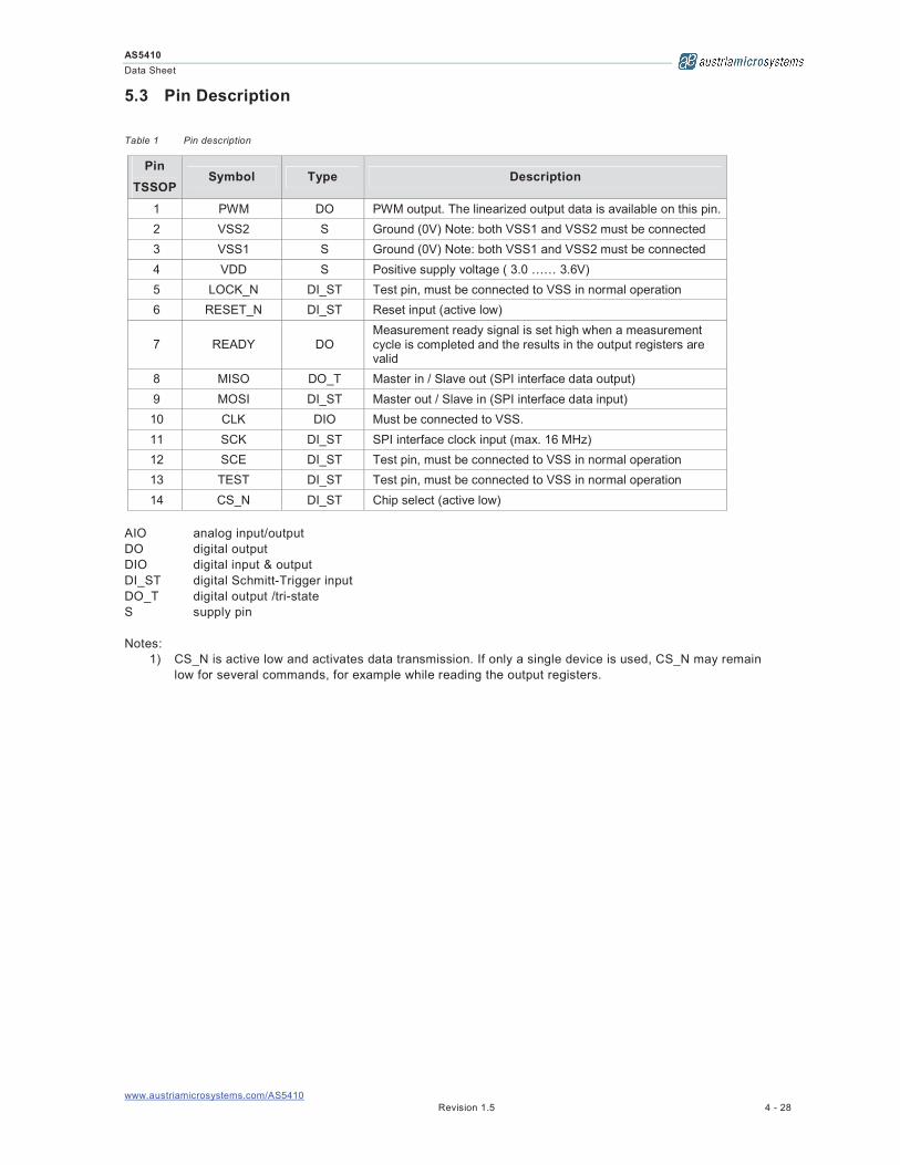
5.3 Pin Description
Table 1 Pin description
Pin
TSSOPSymbol Type Description
1 PWM DO PWM output. The linearized output data is available on this pin.
2 VSS2 S Ground (0V) Note: both VSS1 and VSS2 must be connected
3 VSS1 S Ground (0V) Note: both VSS1 and VSS2 must be connected
4 VDD S Positive supply voltage ( 3.0 …… 3.6V)
5 LOCK_N DI_ST Test pin, must be connected to VSS in normal operation
6 RESET_N DI_ST Reset input (active low)
7 READY DO Measurement ready signal is set high when a measurement cycle is completed and the results in the output registers are valid
8 MISO DO_T Master in / Slave out (SPI interface data output)
9 MOSI DI_ST Master out / Slave in (SPI interface data input)
10 CLK DIO Must be connected to VSS.
11 SCK DI_ST SPI interface clock input (max. 16 MHz)
12 SCE DI_ST Test pin, must be connected to VSS in normal operation
13 TEST DI_ST Test pin, must be connected to VSS in normal operation
14 CS_N DI_ST Chip select (active low)
AIO analog input/output
DO digital output
DIO digital input & output
DI_ST digital Schmitt-Trigger input
DO_T digital output /tri-state
S supply pin
Notes:
1) CS_N is active low and activates data transmission. If only a single device is used, CS_N may remain
low for several commands, for example while reading the output registers.

AS5410
Data Sheet
www.austriamicrosystems.com/AS5410
Revision 1.5 5 - 28
5.4 Power modes
The AS5410 can be configured for two power modes:
• Continuous mode
• Single shot mode
5.4.1 Continuous mode
In this mode, the AS5410 is always active. The chip continuously updates the output registers. The completion
of a new measurement is signalled with pin READY.
5.4.2 Single shot mode
The AS5410 features an automatic power down mode. After completion of a measurement, the chip
automatically suspends to standby. The SPI interface remains active. The control of this mode is possible over
register 000Eh (see chapter 8). A high on the Ready output indicates that a measurement is completed. The
AS5410 suspends to stand-by state after the Ready output has been set.

AS5410
Data Sheet
www.austriamicrosystems.com/AS5410
Revision 1.5 6 - 28
Electrical Characteristics
5.5 Absolute Maximum Ratings
Stresses beyond those listed under “Absolute Maximum Ratings“ may cause permanent damage to the device.
These are stress ratings only. Functional operation of the device at these or any other conditions beyond those
indicated under “Operating Conditions” is not implied. Exposure to absolute maximum rating conditions for
extended periods may affect device reliability.
Table 2 Absolute maximum ratings
Parameter Min Max Unit Comments
DC supply voltage at pin VDD 5 V
Input pin voltage -0.3 VDD +0.3 V
Input current (latchup immunity) -100 100 mA Norm: JEDEC 78
Electrostatic discharge ± 2 kV Norm: MIL 883 E method 3015
Storage temperature -55 150 °C Min – 67°F ; Max +25 7°F
Body temperature 260 °C IPC/JEDEC J-Std-020C
Lead finish 100% Sn “matte tin”
Humidity non-condensing 5 85 %
Moisture Sensitive Level (MSL) 3 Represents a maximum floor time of 168h
EEPROM read/write cycles 100 cycles
5.6 Operating Conditions
Table 3 Electrical characteristics
Operating conditions: operating temperature = -40 to +105°C, VDD = 3.0-3.6V unless otherwise no ted.
Parameter Symbol Min Typ Max Unit Note
Positive Supply voltage VDD 3.0 3.3 3.6 V
Supply current Isupp 15 mA Active operation, continuous mode
Operating ambient temperature
T -40 +105 °C -40°F…+185°F
Internal oscillator frequency fosc 8 MHz
wake up time twu 2 ms from cold start
twlp 200 µs from standby; see 5.4.2
Note: 1)
the conversion time is based on a single phase measurement of one X, Y- or Z sensor. .
5.7 Performance specifications
The AS5410 can be used in linear applications. Shown in 5.7.1 is an example of an absolute linear displacement
sensor for a stroke of 40mm, using Hall elements X0 + X1 (differential) and Z0 + Z1 (differential). The reference
magnet used for this application is described in 5.7.2.

AS5410
Data Sheet
www.austriamicrosystems.com/AS5410
Revision 1.5 7 - 28
side view: X-axis, TSSOP-14:
top view, TSSOP14:
�����
-XX 20mm 20mm
S
side view: Y-axis, TSSOP-14:
N
S N
Pin 1 indicator
Figure 5: Reference setup for absolute linear displacement measurement
5.7.1 System performance specifications
Operating conditions: magnet placement as specified in Figure , operating temperature = -40 to 105°C, VDD = 3.0-3.6V
unless otherwise noted.
Table 4 System Parameters
Parameter Symb
ol
Min Typ Max Unit Note
Lateral stroke dx -20 20 mm using the magnet specified in Figure
Signal amplitude, Bx -60 60 mT
Signal amplitude, By -60 60 mT
Signal amplitude, Bz -50 50 mT
Resolution res 14 Bit @ 40mm stroke
Sampling rate configuration 01)
Ts 1 ms normal mode
Sampling rate configuration 11)
Ts 2 ms slow mode
Accuracy 2)
accvo
0.25 % @ v=0 m/s, 40mm stroke, tamb = 25°C 0.1 mm
-0.5 0.5 % @ v=0 m/s, 40mm stroke, tj = -40 to +105°C -0.2 0.2 mm
accv1
-2.5 2.5 % @ v = 1 m/s, 40mm stroke tamb = 25°C -1 1 mm
accvma
x
-6.5 6.5 % @ v = vmax = 3 m/s, 40mm stroke tamb = 25°C -2.5 2.5 mm
Note: 1)
configurable in register 000Bh2)
The accuracy data is based on an averaged reading (excluding noise) of the displacement value compared to
an absolute reference. Note that with a moving magnet the accuracy is reduced due to the sequential sampling
of the Hall sensors and the conversion time of the ADC. The accuracy values shown in this table are valid for
room temperature.

AS5410
Data Sheet
www.austriamicrosystems.com/AS5410
Revision 1.5 8 - 28
5.7.2 Noise performance specifications
Operating conditions: ambient temperature = 25°C, VDD = 3.0-3.6V
Table 5 Input referred noise
Parameter Symbol Min Typ Max Unit Note
Input referred noise 1)
noiseIN 38 77 µT 3 sigma
Note: 1) AS5410 configuration and setup:
• absolute measurement of Bx and By
• magnetic fields: Bx = 2.5mT, By = 2.5mT (45° CORDI C angle)
• measurement update rate: 1kHz (factory default setting)
5.8 DC Characteristics for Digital Inputs and Outputs
5.8.1 CMOS Schmitt-Trigger Inputs: LOCK_N, RESET_N, CLK, MOSI, SCK, CS_N, Test, SCE
Operating conditions: operating temperature = -40 to +105°C, VDD = 3.0-3.6V unless otherwise no ted.
Parameter Symbol Min Max Unit Note
High level input voltage VIH 1.77 1.87
V VDD = 3.0V
2.07 2.23 VDD = 3.6V
Low level input voltage VIL 1.12 1.27
V VDD = 3.0V
1.42 1.52 VDD = 3.6V
Input current Iin 10 mA for Vin >VDD 1)
Note: 1)
Input pin voltages higher than VDD (e.g. 5V TTL levels) must be limited by a series resistor to ensure
that the maximum input current (Iin) is not exceeded.

AS5410
Data Sheet
www.austriamicrosystems.com/AS5410
Revision 1.5 9 - 28
5.8.2 CMOS Outputs: READY, MISO, PWM
Operating conditions: operating temperature = -40 to +105°C, VDD = 3.0-3.6V unless otherwise no ted.
Parameter Symbol Min Max Unit Note
Output high level VOH 2.5 VDD V
Output current, source IOH 8 mA
Output low level VOL 0 0.4 V
Output current, sink IOL 8 mA
5.8.3 Power On reset
Operating conditions: operating temperature = -40 to +105°C
Parameter Symbol Min Typ Max Unit Note
Reset threshold; VDD level rising Von 1.24 2.26 2.82 V
Reset threshold; VDD level falling Voff 1.13 2.67 V
5.9 On-chip temperature measurement
The AS5410 provides a linear on-chip temperature sensor which is use for automatic compensation of sensitivity
and offset drifts for the Hall-In-One sensors.
The measured chip temperature is available in a register (0110h) and can be used for monitoring purposes
Operating conditions: operating temperature = -40 to +105°C
Parameter Symbol Min Typ Max Unit Note
Temperature signal at 25° D temp 0 LSB
Resolution Restemp 185 200 210 LSB/K
6 Serial Interface (SPI) The SPI interface provides data transfer between AS5410 and the external microcontroller.
The Interface is conform to the SPI standard.
Note that SPI bus is a de facto standard, rather than one agreed by any international committee.
The minimum number of connections between microcontroller and AS5410 is three:
1) MOSI: Master Out – Slave In; data transfer from microcontroller to AS5410 (Write)
2) MISO: Master In – Slave Out; data transfer from AS5410 to microcontroller (Read)
3) SCK: Serial clock; Data is written and read with the rising edge of SCK
Optionally, two further connections may be used:
1) CS_N: Chip select; this connection is mandatory when multiple AS5410 devices are connected in
parallel. In electrically “noisy” environment it is recommended to use the CS_N connection in order to
maintain safe data transfer.
For a single unit, this connection is optional as the data transmission is synchronized automatically by
the number of SCK cycles. In this case it is recommended to verify the synchronization by CRC (see
Error! Reference source not found.), Data readback (Figure ) or repeated reading and cross-checking
of subsequent measurements.
2) Ready: this output indicates when data is ready, it is cleared by reading data from address 0100h or
0122h

AS5410
Data Sheet
www.austriamicrosystems.com/AS5410
Revision 1.5 10 - 28
Figure 6: Hardware connection between AS5410 and microcontroller
Figure 7: SPI timing diagram
The data bits sent to the chip via MOSI and the data bits received from the chip via MISO are defined as follows
(see also Figure ):
A15….A00 = 16-bit register address
W15….W00 = 16-bit write data (in write mode)
X15….X00, Y15 = 16-bit read data or previous command (depending on mode)
R15…R0 = 16-bit read data in read mode or previous data in write mode
Parameter Symbol Min Typ Max Unit Note
SCK frequency fsck 0 16 MHz
SCK pulse width HI tSCKhi 15 ns
SCK pulse width LO tSCKlo 15 ns
SCK setup time before data read tA2DRs 15 ns
CS_N enable setup time before SCK tCSEs 10 ns
CS_N enable hold time after SCK tCSEh 10 ns
CS_N disable setup time before SCK tCSDs 10 ns
CS_N disable hold time after SCK tCSDh 10 ns
MOSI setup time before SCK tMOSIs 10 ns
MOSI hold time after SCK tMOSIh 10 ns
MISO delay after SCK tMISOd 10 ns
MISO enable delay after CS_N tMISOEd 10 ns
MISO high Z delay after CS_N tMISOZd 10 ns
Output edge rise time tOr 3 ns
Output edge fall time tOf 3 ns
µC AS5410
MOSI
MISO
SCK
SS/
MISO
MOSI
SCK
CS_N
ReadyReady
optional wiring
mandatory
wiring

AS5410
Data Sheet
www.austriamicrosystems.com/AS5410
Revision 1.5 11 - 28
7 Data transfer between AS5410 and Microcontroller Data is transferred to the AS5410 via the MOSI pin (Master Out – Slave In) with the rising edge of SCK.
Data is read from the AS5410 from the MISO pin (Master In – Slave Out) with the rising edge of SCK.
The data format consists of data streams with 32 bit in length. The first 16 bits define a 16-bit address and the
subsequent 16 bits contain read or write data.
The MSB of the address word A<15> defines the direction of data transfer:
A<15> = 0 READ; data transfer from AS5410 to microcontroller; read measurement data
A<15> = 1 WRITE; data transfer from microcontroller to AS5410; write configuration data
Figure 8: Data transfer between AS5410 and microcontroller
7.1 Read mode
For reading a register, the 16-bit Read address (with A<15>=0) is sent to the MOSI pin. After 16 SCK cycles,
data of the specified address is read from the MISO pin (see Figure ). At the same time, the new address may
be clocked into the MOSI pin.
7.1.1 Continuous measurement
It is possible to continuously read data from the AS5410 even if a new measurement is not yet finished. In this
case, the last measurement data will be read. As soon as a new measurement is completed, it will be available
at the SPI interface.
7.2 Write mode & readback
For additional safety and detection of communication errors, the actual contents of a register may be read at the
same time as new data is written to this register.
In case of a Write command, the 16-bit Write address (with A<15>=1) is sent to the MOSI pin. After 16 SCK
cycles, data following the address bits is written to the specified address via MOSI in (see Figure ) At the same
time, the present data of that register may be read from the MISO pin. Following the 16-bit of data (Data 1 in
Figure ), a new address may be written to the AS5410. While the new address is written, the address from the
previous command is available at the MISO output.
7.3 Checksum
To avoid reading errors, the IC calculates a Checksum at every read cycle from the register content. The
Checksum value is built by an XOR operation of the previous Checksum value and the read register content.
The CRC is calculated every time a register is read.
By choosing how often the Checksum is read and rechecked by the master it is possible to adjust the
communication speed and safety level.
The Checksum value is stored in register 0108h (see chapter 8).

AS5410
Data Sheet
www.austriamicrosystems.com/AS5410
Revision 1.5 12 - 28
8 Register contents The following registers can be addressed by the user via the SPI interface. Each register is 16-bit wide.
Registers not listed in the table below must not be modified from their factory programmed setting.
Note: “r” are reserved bits, they must not be modified (unless otherwise noted)
8.1 Register 000Bh:
This register controls the sequencer
Register Access Bit Function Default Note
000Bh:
Sequencer
control
R/W
D15 (MSB) r 0
D14 r 0
D13 r 0
D12 r 0
D11 MgRangExt 0
“Magnet Range Extension”
Enable the algorithm for an extended position range.
1 = Magnet Range Extension enabled
0 = Magnet Range Extension disabled
D10 CoordSel 0
�Coordinate System Selection”
1 = The sign of the Lin Ang (Register 0122h) gets
changed if MagDir (Register 000Bh) = 1
0 = Lin Ang (Register 0122h) gets not changed
D9 r 0
D8 r 0
D7 Table
Select 0 0
These bits allow the selection of 4 different operating modes, stored in 4 individual sequencer tables
D6 Table
Select 1 0
D5 MagDir 0
This Bit allows to switch the magnet direction
MagDir = 0: North pole must point in +x direction (pin 7
to pin1) Default/powerup mode.
MagDir = 1: North pole must point in -x direction (pin1 to pin7). Preferred orientation to permit use of CoordSel bit.
D4 DiffMd 0 Differential mode: 0 = absolute measurement of Hall cells, 1 = differential measurement of Hall cells
D3 r 0
D2 r 0
D1 RdyHZ 0
READY Tri-State:
0: The READY pin is always active. It must NOT be connected in parallel
1: The READY output may be connected in parallel. It is normally in high Z and only active (high) if the IC is addressed and selected. (Note: a 10k pull down resistor is mandatory at the common READY signal line if RdyHz = 1 !)
D0 (LSB) r 0

AS5410
Data Sheet
www.austriamicrosystems.com/AS5410
Revision 1.5 13 - 28
Table 0 Table 1 Table 2 Table 3
Differential Mode
1 kHz Sample Rate
Differential Mode
0.5 kHz Sample Rate
Absolut Pixel1
1 kHz Sample Rate
Absolut Pixel1
0.5 kHz Sample Rate
Cordic
Input
values
Pixelcell0, Bz0 = 0x112h
- Pixelcell1, Bz1 = 0x111h
Pixelcell0, Bx0 = 0x114h
- Pixelcell1, Bx1 = 0x113h
Pixelcell0, Bz0 = 0x112h
- Pixelcell1, Bz1 = 0x111h
Pixelcell0, Bx0 = 0x114h
- Pixelcell1, Bx1 = 0x113h
Pixelcell1, Bz1 = 0x111h
Pixelcell1, Bx1 = 0x113h
Pixelcell1, Bz1 = 0x111h
Pixelcell1, Bx1 = 0x113h
Register
B
Settings
Table Select 1…Table Select
0 = 00 (mandatory)
DiffMd = 1 (mandatory)
MgRangExt = 0 or 1
depending on application
Table Select 1…Table Select
0 = 01 (mandatory)
DiffMd = 1 (mandatory)
MgRangExt = 0 or 1
depending on application
Table Select 1…Table
Select 0 = 10 (mandatory)
DiffMd = 0 (mandatory)
MgRangExt = 0
(mandatory)
Table Select 1…Table
Select 0 = 11 (mandatory)
DiffMd = 0 (mandatory)
MgRangExt = 0
(mandatory)
8.2 Register 000Dh:
Register Access Bit Function Default Note
000Dh: R/W
D15 (MSB) PWMLimitHi 5 1
PWM Limit High
Limits the PWM duty cycle to a maximum value
D14 PWMLimitHi 4 1
D13 PWMLimitHi 3 0
D12 PWMLimitHi 2 0
D11 PWMLimitHi 1 1
D10 PWMLimitHi 0 1
D9 PWMLimitLo 5 0
PWM Limit Low
Limits the PWM duty cycle to a minimum value
D8 PWMLimitLo 4 0
D7 PWMLimitLo 3 1
D6 PWMLimitLo 2 1
D5 PWMLimitLo 1 0
D4 PWMLimitLo 0 1
D3 PWMEn 0 PWM Enable, Enables the PWM output
D2 PWM PreScale 2 0
PWM PreScale, Sets PWM frequency and resolution D1 PWM PreScale 1 1
D0 (LSB) PWM PreScale 0 1
8.3 Register 000Eh:
This register holds the sequencer control bits
Register Access Bit Function Default Note
000Eh:
Sequencer
control
R/W
D15 (MSB) – D2
r 0
D1 Seq 1 Sequencer Enable
D0 (LSB) SL 0 Single Loop

AS5410
Data Sheet
www.austriamicrosystems.com/AS5410
Revision 1.5 14 - 28
8.4 Register 000Fh:
This register holds the threshold and hysteresis of the Cordic magnitude value (see register 0120h), at which the
“Magnet Lost” flag in register 0107h is set/cleared.
Register Access Bit Function Default Note
000Fh: R/W
D15 (MSB) r 0
reserved
D14 r 0
D13 r 0
D12 r 0
D11 r 0
H2 Hyst� 0
Hysteresis for “magnet lost” H1 Hyst 0
H0 Hyst 1
V7 MgnLostLmt� 0
Magnet lost threshold value compared to register 0121h
V6 MgnLostLmt 0
V5 MgnLostLmt 0
V4 MgnLostLmt 0
V3 MgnLostLmt 0
V2 MgnLostLmt 0
V1 MgnLostLmt 1
V0 (LSB) MgnLostLmt 1
V7…V0: The minimum allowed Magnitude of Cordic can be selected. The binary number, represented by
V7...V0 must be multiplied with 64 to calculate the minnumum allowed Magnitude of Cordic.
Example:
Select V0 and V1.
binary decimal
V7 V6 V5 V4 V3 V2 V1 V0
0 0 0 0 0 0 1 1 3
�
The coresdponding dual number to 00000011 is 3 this number multiplied with 64 ist the minimum allowed
Magnitude of Crodic.
64 * 3 = 192 = Threshold limit
If the magnitude of cordic turns under 192 the MagLost bit in register 0107h will turn form 0 to 1.
H2…H0: The Hysteresis arround the minimum allowed Magnitude of Cordic can be selected.
The HysteresisHystd is calclulated by the Formular
Hyst…Hysteresis value in Register 000Fh
Hystd …decimal Hysteresis value arround the minimum allowed Magnitude of Cordic
MgnLostLmt …the Threshold limit as calculated in the example above.
HystMgnLostLmtHystd
2
1⋅=
Example:
Select H0
binary decimal
H2 H1 H0
0 0 1 1
�

AS5410
Data Sheet
www.austriamicrosystems.com/AS5410
Revision 1.5 15 - 28
962
1192
2
11
=⋅=⋅=Hyst
MgnLostLmtHystd
Now the MagLost bit in register 0107h will turn form 0 to 1 at a Magnitude of Cordic value lower than 192. After
the MagLost bit is 0 it turns back to 1 at a value higher than 288, because 192 + 96 = 288.
8.5 Register 0030h:
E²PROM address
Register Access Bit Function Note
0030h:
E²PROM address
R/W
D15 (MSB) A15
To read/write E²PROM contents, the selected E²PROM address must be specified in this register.
The corresponding data is available in register 0031h.
For write operations, status bit ED in register 0107h which indicates the completion of a write operation must be verified before starting a new write cycle.
Writing 16 bits of data requires ~20ms
D14 A14
D13 A13
D12 A12
D11 A11
D10 A10
D9 A9
D8 A8
D7 A7
D6 A6
D5 A5
D4 A4
D3 A3
D2 A2
D1 A1
D0 (LSB) A0
8.6 Register 0031h:
E²PROM data
Register Access Bit Function Note
0031h:
E²PROM data
R/W
D15 (MSB) D15
This register holds the E²PROM contents of the address selected in register 0030h
D14 D14
D13 D13
D12 D12
D11 D11
D10 D10
D9 D9
D8 D8
D7 D7
D6 D6
D5 D5
D4 D4
D3 D3
D2 D2
D1 D1
D0 (LSB) D0

AS5410
Data Sheet
www.austriamicrosystems.com/AS5410
Revision 1.5 16 - 28
8.7 Register 0107h:
Status register; this register holds various status flags
Register Access Bit Function Note
0107h:
Status R
D15 (MSB) RDY
Indicates completion of a new measurement; same function as the “Ready” output pin. 0 = calculation is in progress or chip not ready 1 = measurement completed, new measurement data is stored in register 0110h-0114h and 0120h-0122h
D14 MagLost 1 = Magnetic field values are too low for position measurement; the threshold level can be selected at Register 000Fh Bit D7…D0
D13 CorrOvfl Ambiguous angle correction overflow
D12 NormOvfl Normalizing scale overflow
D11 SensOvfl Overflow during sensitivity correction over temperature
D10 RngWarn ADC overflow
D9 HistWarn Histogram failure during ADC operation
D8 CalcError Or wired combination of RngWarn, HistWarn, NormOvfl, SensOvfl
D7 D7 -reserved-
D6 D6 -reserved-
D5 D5 -reserved-
D4 D4 -reserved-
D3 D3 -reserved-
D2 D2 -reserved-
D1 MagDir Detected or chosen orientation of Magnet
D0 (LSB) ED E²PROM write cycle: 0 = E²PROM write cycle in progress 1= E²PROM write cycle completed
8.8 Register 0108h:
Cycle Redundancy Check (CRC):
Register Access Bit Function Note
0108h:
CRC R
D15 (MSB) CRC15
Checksum Reading Check
D14 CRC14
D13 CRC13
D12 CRC12
D11 CRC11
D10 CRC10
D9 CRC9
D8 CRC8
D7 CRC7
D6 CRC6
D5 CRC5
D4 CRC4
D3 CRC3
D2 CRC2
D1 CRC1
D0 (LSB) CRC0

AS5410
Data Sheet
www.austriamicrosystems.com/AS5410
Revision 1.5 17 - 28
8.9 Register 0110h:
On-chip temperature sensor:
Register Access Bit Function Note
0110h:
Tempera-ture
R
D15 (MSB) T15
on-chip temperature sensor
Temperature[°C] = (Register110h / 200) + 25
D14 14
D13 T13
D12 T12
D11 T11
D10 T10
D9 T9
D8 T8
D7 T7
D6 T6
D5 T5
D4 T4
D3 T3
D2 T2
D1 T1
D0 (LSB) T0

AS5410
Data Sheet
www.austriamicrosystems.com/AS5410
Revision 1.5 18 - 28
8.10 Register 0111h:
Magnetic field of Pixel cell 1; Z field sensor cell
Register Access Bit Function Note
0111h:
Magnetic field value
R
D15 (MSB)
Bz1� Magnetic field Bz of Pixel-cell 1
D14
D13
D12
D11
D10
D9
D8
D7
D6
D5
D4
D3
D2
D1
D0 (LSB)
8.11 Register 0112h:
Magnetic field of Pixel cell 0; Z field sensor cell
Register Access Bit Function Note
0112h:
Magnetic field value
R
D15 (MSB)
Bz0 Magnetic field Bz of Pixel-cell 0
D14
D13
D12
D11
D10
D9
D8
D7
D6
D5
D4
D3
D2
D1
D0 (LSB)

AS5410
Data Sheet
www.austriamicrosystems.com/AS5410
Revision 1.5 19 - 28
8.12 Register 0113h:
Magnetic field of Pixel cell 1; X field sensor cell
Register Access Bit Function Note
0113h:
Magnetic field value
R
D15 (MSB)
Bx1 Magnetic field Bx of Pixel-cell 1
D14
D13
D12
D11
D10
D9
D8
D7
D6
D5
D4
D3
D2
D1
D0 (LSB)
8.13 Register 0114h:
Magnetic field of Pixel cell 0; X field sensor cell
Register Access Bit Function Note
0114h:
Magnetic field value
R
D15 (MSB)
Bx0 Magnetic field Bx of Pixel-cell 0
D14
D13
D12
D11
D10
D9
D8
D7
D6
D5
D4
D3
D2
D1
D0 (LSB)

AS5410
Data Sheet
www.austriamicrosystems.com/AS5410
Revision 1.5 20 - 28
8.14 Register 0120h:
Cordic magnitude value; this is representing the strength of the magnetic field, as calculated by the Cordic.
These values may for example be used to check the magnet for out-of-range conditions, or to issue a
“weak magnetic field” warning when the value gets below a certain threshold
8.15 Register 0121h:
Cordic angle value; this is representing the (non-linearized) angle or direction of the magnetic field, as calculated
by the Cordic.
Register Access Bit Function Note
0121h:
Angle R
D15 (MSB)
Ang
Ang [°]…angle value of cordic [°]
h0121 � angle value of cordic [LSB]
MgRangExt = 0:
Ang [°] h012165536
360∗=
MgRangExt = 1:
Ang [°] h012165536
576∗=
D14
D13
D12
D11
D10
D9
D8
D7
D6
D5
D4
D3
D2
D1
D0 (LSB)
Register Access Bit Function Note
0120h:
Magnitude R
D15 (MSB)
Mag
Magnitude value of cordic
Calculation in absolute mode (DiffMd = 0)
220113011182338.00120 hhh +∗=
Calculation in differential mode (DiffMd = 1)
22 )01130114()01110112(82338.00120 hhhhh −+−∗=
D14
D13
D12
D11
D10
D9
D8
D7
D6
D5
D4
D3
D2
D1
D0 (LSB)

AS5410
Data Sheet
www.austriamicrosystems.com/AS5410
Revision 1.5 21 - 28
8.16 Register 0122h:
This register holds the final, calculated and linearized position information
Register Access Bit Function Note
0122h:
Position R
D15 (MSB)
LinAng
This register holds the linearized 16-bit position information.
LinAng [°]…linearized 16-bit position information [ °]
h0121 � linearized 16-bit position information [LSB]
MgRangExt = 0:
LinAng [°] h012265536
360∗=
MgRangExt = 1:
LinAng [°] h012265536
576∗=
D14
D13
D12
D11
D10
D9
D8
D7
D6
D5
D4
D3
D2
D1
D0 (LSB)
8.17 EEPROM Linearization Table 005Fh to 007Fh
The data output of the Cordic can be linerarized using the 33 points stored in the EEPORM
Register Content Note
005Fh Angle linearization table, value 16
Applied to Cordic Output
0060h Angle linearization table, value 0
0061h Angle linearization table, value 1
… …
006Fh Angle linearization table, value 15
0070h Angle linearization table, value -16
0071h Angle linearization table, value -15
… …
007Eh Angle linearization table, value -2
007Fh Angle linearization table, value -1

AS5410
Data Sheet
www.austriamicrosystems.com/AS5410
Revision 1.5 22 - 28
9 Magnet features
9.1 Magnet Range Extension
If the magnet is far away from the sensor, the field vectors in the sensor position can generate false angle information.
By exploiting the magnetic field behaviour it is still possible to calculate correct position information. As absolute field
values are used during this calculation external disturbance fields must not exceed a maximum of approximately ten
times the terrestrial magnetic field. The position range extending calculation method can be disabled if large
disturbance fields occur during operation.
MgRangExt = 0: angles between -180° and +180° can b e measured
MgRangExt = 1: angles between -288° and +288° can b e measured
Register Access Bit Function Note
000Bh:
Sequencer
control
R/W
D11 MgRangExt “Magnet Range Extension”
Enable the algorithm for an extended position range.
D10 CoordSel
“Coordinate System Selection”
1 = The sign of the LinAng (Register 0122h) gets
changed if MagDir (Register 000Bh) = 1
0 = LinAng (Register 0122h) gets not changed
Notes:
2) Pins LOCK_N and SCE are test pins for factory testing. They must be connected to VSS in normal
operation to prevent accidental enabling of a test mode
3) Output READY is set high when a measurement cycle is completed and the results in the output
registers are valid. It is cleared by reading data from address 0100h or 0122h
4) CLK allows monitoring of the internal clock or applying an external clock.
5) Output MISO is only activated when CS_N is low. It is in high impedance state otherwise, this allows
parallel operation of multiple ICs.
6) CS_N is active low and activates data transmission. If only a single device is used, CS_N may remain
low for several commands, for example while reading the output registers.

AS5410
Data Sheet
www.austriamicrosystems.com/AS5410
Revision 1.5 23 - 28
10 PWM data transmission
In addition to the SPI interface, the AS5410 offers a PWM output that provides data transmission of the linearized output data over a single wire. The base frequency of the PWM is the system clock frequency, so one PWM digit always corresponds to approx. 125ns. The PWM resolution is set by 3 bits (PWMPreScale) which shift the 16 bit wide angle value by 0 to 7 digits.The duty cycle of the PWM signal lies between 0….100%. In case of an error, the duty cycle is 0%.
If Register 0122h value increases the duty cycle decreases. If Register 0122h value decreases the duty cycle
increases.
Register Access Bit Function Note
000Dh:
PWM settings
R/W
D15-10 PWMLimitHi
<5:0>
PWM Limit High
Limits the PWM duty cycle to a maximum value
D9-4 PWMLimitLo
<5:0>
PWM Limit Low
Limits the PWM duty cycle to a minimum value
D3 PWMEn PWM Enable, Enables the PWM output
D2-0 PWMPreScale
<2:0>
PWM PreScale, Sets PWM frequency and resolution
µC AS5410PWM PWM
VDD VDD
GND VSS
VDD= 3.0 - 3.6V
Figure 9: Single pin data transmission connection diagram
PWM
Duty Cycle
[%]
Register 122h
(Linear Angle)
[LSB]
0 32767
50 0
100 -32768
��
Between 0%...100% the duty cycle is linear to the Linear Angle.
PWM Enable: Must be set high to enable the PWM mode.
PWMPreScale0…PWMPreScale3: The PWM resolution is set by those 3 Bits.
PWMPreScale0…
PWMPreScale3
Resolutio
n (bit)
PWM (kHz)
000 16 0.122
001 15 0.244
010 14 0.488
011 13 0.977
100 12 1.953
101 11 3.906
110 10 7.813
111 9 15.63

AS5410
Data Sheet
www.austriamicrosystems.com/AS5410
Revision 1.5 24 - 28
PWMLimitHi5…PWMLimitHi0: Limits the PWM duty cycle.
duty cycle PWMLimitHi0…PWMLimitHi5
minimum 50% 000000
minimum 0% 111111 �
�
Between 0%...50% the duty cycle limit is linear to the binary values selected by PWMLimitHi5…PWMLimitHi0.
The limits are clamping limits (by selecting limits the resolution decreases).
PWMLimitLo5…PWMLimitLo0: Limits the PWM duty cycle. �
duty cycle PWMLimitLo0…PWMLimitLo5
maximum 50% 111111
maximum 100% 000000 �
Between 50%...100% the duty cycle limit is linear to the binary values selected by
PWMLimitLo5…PWMLimitLo0. The limits are clamping limits (by selecting limits the resolution decreases).
�
Example Table:
clamping range 0% – 100% PWM
duty cycle
10% – 90% PWM
duty cycle
50% – 50% PWM
duty cycle
PWMLimitHi5 1 1 0
PWMLimitHi4 1 1 0
PWMLimitHi3 1 0 0
PWMLimitHi2 1 0 0
PWMLimitHi1 1 1 0
PWMLimitHi0 1 0 0
PWMLimitLo5 0 0 1
PWMLimitLo4 0 0 1
PWMLimitLo3 0 1 1
PWMLimitLo2 0 1 1
PWMLimitLo1 0 0 1
PWMLimitLo0 0 1 1

AS5410
Data Sheet
www.austriamicrosystems.com/AS5410
Revision 1.5 25 - 28
Package Drawings and Markings
10.1 Pixel cell placement

AS5410
Data Sheet
www.austriamicrosystems.com/AS5410
Revision 1.5 26 - 28
10.2 14-Lead Thin Shrink Small Outline Package TSSOP-14
�
��
�
�
��
��
�
�
����
�� ���
Figure 11: TSSOP-14 Package Dimensions and Marking
Dimensions
���������� ���
��� ��� ���� ��� ��� ����
�� � � �� � � ���
�� �� � �� �� �� ��
��� �� � �� �� ��� ��
!� �� � �� �� � ��
�� � �� �� � � ��� ��� ��
�� � �� � �� � �� ���� ���� ���
�� � �� � �� � ��� ��� ��� ���
"� ��� ����
Table 6: Package Dimensions
Marking: YYWWIZZ
YY: Last Digit of Manufacturing Year
WW: Manufacturing Week
I: Plant Identifier
ZZ: Traceability Code
Thermal Resistance Rth(j-a):
89 K/W in still air, soldered on PCB
IC's marked with a white dot or the
letters "ES" denote Engineering
Samples

AS5410
Data Sheet
www.austriamicrosystems.com/AS5410
Revision 1.5 27 - 28
Ordering Information
The devices are available as standard products, shown in Table 7.
Model Description Delivery
Form Package
AS5410TSU
AS5410TST
Three-Dimensional Hall Encoder Tubes
Tape & Reel
TSSOP 14
TSSOP 14
Table 7: Ordering Information
10.3 Revision History
RevisionDescription
Change
date
1.0 Released preliminary version May.30.2011
1.1 Additional information added Jun.05.2011
1.2 Additional information added Jan.12.2012
1.5 Chapter 10: example table corrected Apr.06.2012
Table 8: revision history

AS5410
Data Sheet
www.austriamicrosystems.com/AS5410
Revision 1.5 28 - 28
11 Copyrights Copyright © 2011, austriamicrosystems AG, Schloss Premstaetten, 8141 Unterpremstaetten, Austria – Europe.
Trademarks Registered ®. All rights reserved. The material herein may not be reproduced, adapted, merged,
translated, stored, or used without the prior written consent of the copyright owner.
All products and companies mentioned are trademarks or registered trademarks of their respective companies.
12 Disclaimer Devices sold by austriamicrosystems AG are covered by the warranty and patent indemnification provisions
appearing in its Term of Sale. austriamicrosystems AG makes no warranty, express, statutory, implied, or by
description regarding the information set forth herein or regarding the freedom of the described devices from
patent infringement. austriamicrosystems AG reserves the right to change specifications and prices at any time
and without notice. Therefore, prior to designing this product into a system, it is necessary to check with
austriamicrosystems AG for current information. This product is intended for use in normal commercial
applications. Applications requiring extended temperature range, unusual environmental requirements, or high
reliability applications, such as military, medical life-support or lifesustaining equipment are specifically not
recommended without additional processing by austriamicrosystems AG for each application.
The information furnished here by austriamicrosystems AG is believed to be correct and accurate. However,
austriamicrosystems AG shall not be liable to recipient or any third party for any damages, including but not
limited to personal injury, property damage, loss of profits, loss of use, interruption of business or indirect,
special, incidental or consequential damages, of any kind, in connection with or arising out of the furnishing,
performance or use of the technical data herein. No obligation or liability to recipient or any third party shall arise
or flow out of austriamicrosystems AG rendering of technical or other services.
Contact Information
Headquarters
austriamicrosystems AG
A-8141 Schloss Premstaetten, Austria
Tel: +43 (0) 3136 500 0
Fax: +43 (0) 3136 525 01
For Sales Offices, Distributors and Representatives, please visit:
http://www.austriamicrosystems.com/contact