Embed Size (px)
Citation preview
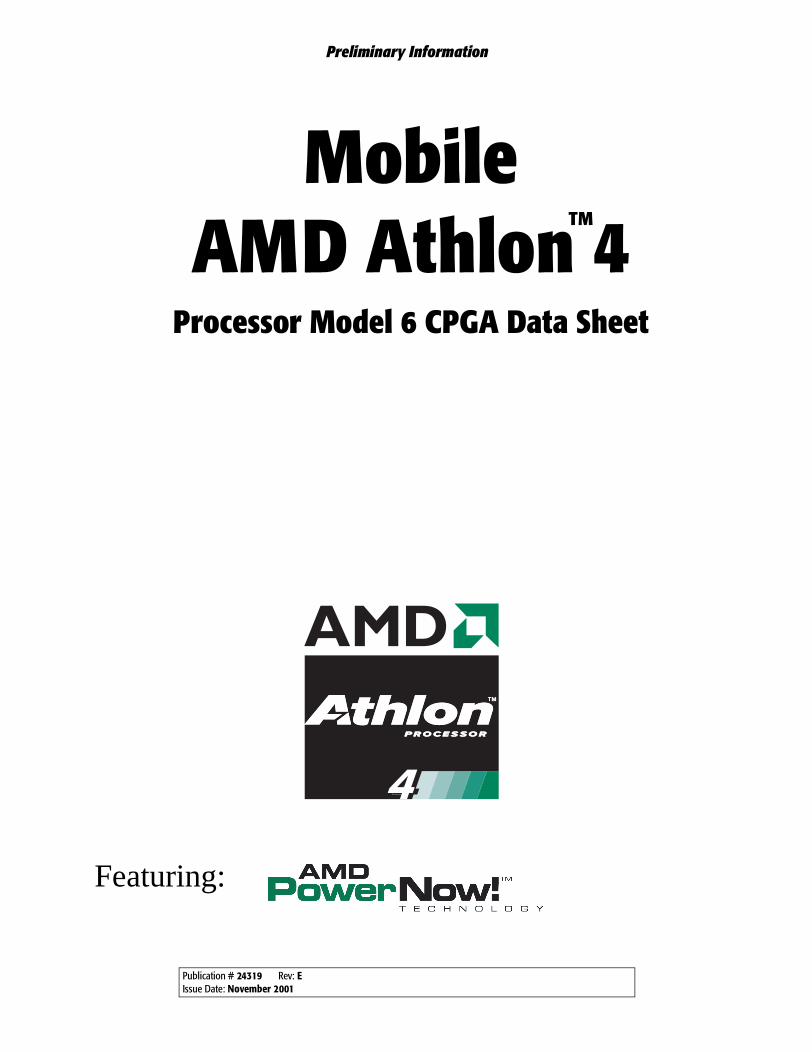
Preliminary Information
Mobile AMD Athlon 4
Processor Model 6 CPGA Data Sheet
Publication # 24319 Rev: EIssue Date: November 2001
TM
Featuring:

Preliminary Information
Trademarks
AMD, the AMD Arrow logo, AMD Athlon, AMD Duron, and combinations thereof, AMD PowerNow!, and 3DNow!are trademarks of Advanced Micro Devices, Inc.
HyperTransport is a trademark of the HyperTransport Technology Consortium.
MMX is a trademark of Intel Corporation.
Other product names used in this publication are for identification purposes only and may be trademarks oftheir respective companies.
© 2000, 2001 Advanced Micro Devices, Inc. All rights reserved.The contents of this document are provided in connection with AdvancedMicro Devices, Inc. (“AMD”) products. AMD makes no representations orwarranties with respect to the accuracy or completeness of the contents ofthis publication and reserves the right to make changes to specifications andproduct descriptions at any time without notice. No license, whether express,implied, arising by estoppel or otherwise, to any intellectual property rightsis granted by this publication. Except as set forth in AMD’s Standard Termsand Conditions of Sale, AMD assumes no liability whatsoever, and disclaimsany express or implied warranty, relating to its products including, but notlimited to, the implied warranty of merchantability, fitness for a particularpurpose, or infringement of any intellectual property right.
AMD’s products are not designed, intended, authorized or warranted for useas components in systems intended for surgical implant into the body, or inother applications intended to support or sustain life, or in any other applica-tion in which the failure of AMD’s product could create a situation where per-sonal injury, death, or severe property or environmental damage may occur.AMD reserves the right to discontinue or make changes to its products at anytime without notice.

24319E—November 2001 Mobile AMD Athlon™ 4 Processor Model 6 CPGA Data Sheet
Preliminary Information
Contents
List of Figures . . . . . . . . . . . . . . . . . . . . . . . . . . . . . . . . . . . . . . . . . . . . vii
List of Tables . . . . . . . . . . . . . . . . . . . . . . . . . . . . . . . . . . . . . . . . . . . . . . ix
Revision History . . . . . . . . . . . . . . . . . . . . . . . . . . . . . . . . . . . . . . . . . . .xi
1 Overview . . . . . . . . . . . . . . . . . . . . . . . . . . . . . . . . . . . . . . . . . . . . 1
1.1 Processor Microarchitecture Summary . . . . . . . . . . . . . . . . . . 2
2 Interface Signals . . . . . . . . . . . . . . . . . . . . . . . . . . . . . . . . . . . . . 5
2.1 Overview . . . . . . . . . . . . . . . . . . . . . . . . . . . . . . . . . . . . . . . . . . . 52.2 Signaling Technology . . . . . . . . . . . . . . . . . . . . . . . . . . . . . . . . . 52.3 Push-Pull (PP) Drivers . . . . . . . . . . . . . . . . . . . . . . . . . . . . . . . . 62.4 AMD Athlon™ System Bus Signals . . . . . . . . . . . . . . . . . . . . . . 6
3 Logic Symbol Diagram . . . . . . . . . . . . . . . . . . . . . . . . . . . . . . . . 7
4 Power Management . . . . . . . . . . . . . . . . . . . . . . . . . . . . . . . . . . 9
4.1 Power Management States . . . . . . . . . . . . . . . . . . . . . . . . . . . . 9Working State . . . . . . . . . . . . . . . . . . . . . . . . . . . . . . . . . . . . . . 10Halt State . . . . . . . . . . . . . . . . . . . . . . . . . . . . . . . . . . . . . . . . . . 10Stop Grant States. . . . . . . . . . . . . . . . . . . . . . . . . . . . . . . . . . . . 11Probe State. . . . . . . . . . . . . . . . . . . . . . . . . . . . . . . . . . . . . . . . . 13FID_Change State . . . . . . . . . . . . . . . . . . . . . . . . . . . . . . . . . . . 13Processor Performance States and the FID_Change Protocol. . . . . . . . . . . . . . . . . . . . . . . . . . . . . . . . . . . . . . . . . . . . 13
4.2 Connect and Disconnect Protocol . . . . . . . . . . . . . . . . . . . . . . 18Connect Protocol . . . . . . . . . . . . . . . . . . . . . . . . . . . . . . . . . . . . 18Connect State Diagram. . . . . . . . . . . . . . . . . . . . . . . . . . . . . . . 22
4.3 Clock Control . . . . . . . . . . . . . . . . . . . . . . . . . . . . . . . . . . . . . . 244.4 SYSCLK Multipliers . . . . . . . . . . . . . . . . . . . . . . . . . . . . . . . . . 244.5 Special Cycles . . . . . . . . . . . . . . . . . . . . . . . . . . . . . . . . . . . . . . 27
5 CPUID Support . . . . . . . . . . . . . . . . . . . . . . . . . . . . . . . . . . . . . 29
6 Thermal Design . . . . . . . . . . . . . . . . . . . . . . . . . . . . . . . . . . . . . 31
7 Electrical Data . . . . . . . . . . . . . . . . . . . . . . . . . . . . . . . . . . . . . . 33
7.1 Conventions . . . . . . . . . . . . . . . . . . . . . . . . . . . . . . . . . . . . . . . 337.2 Interface Signal Groupings . . . . . . . . . . . . . . . . . . . . . . . . . . . 337.3 Soft Voltage Identification (SOFTVID[4:0]) . . . . . . . . . . . . . 357.4 Frequency Identification (FID[3:0]) . . . . . . . . . . . . . . . . . . . . 357.5 VCCA AC and DC Characteristics . . . . . . . . . . . . . . . . . . . . . 367.6 Decoupling . . . . . . . . . . . . . . . . . . . . . . . . . . . . . . . . . . . . . . . . 367.7 Valid Voltage and Frequency Combinations . . . . . . . . . . . . . 377.8 VCC_CORE AC and DC Characteristics . . . . . . . . . . . . . . . . 38
Table of Contents iii

Mobile AMD Athlon™ 4 Processor Model 6 CPGA Data Sheet 24319E—November 2001
Preliminary Information
7.9 Absolute Ratings . . . . . . . . . . . . . . . . . . . . . . . . . . . . . . . . . . . 407.10 VCC_CORE Voltage and Current . . . . . . . . . . . . . . . . . . . . . . 417.11 SYSCLK and SYSCLK# AC and DC Characteristics . . . . . . 427.12 AMD Athlon System Bus AC and DC Characteristics . . . . . 447.13 General AC and DC Characteristics . . . . . . . . . . . . . . . . . . . . 467.14 Open Drain Test Circuit . . . . . . . . . . . . . . . . . . . . . . . . . . . . . 487.15 Thermal Diode Characteristics . . . . . . . . . . . . . . . . . . . . . . . . 497.16 Reserved Pins DC Characteristics . . . . . . . . . . . . . . . . . . . . . 527.17 FID_Change Induced PLL Lock Time . . . . . . . . . . . . . . . . . . 52
8 Signal and Power-Up Requirements . . . . . . . . . . . . . . . . . . . . 53
8.1 Power-Up Requirements . . . . . . . . . . . . . . . . . . . . . . . . . . . . . 53Signal Sequence and Timing Description . . . . . . . . . . . . . . . . 53Clock Multiplier Selection (FID[3:0]) . . . . . . . . . . . . . . . . . . . 56
8.2 Processor Warm Reset Requirements . . . . . . . . . . . . . . . . . . 56Mobile AMD Athlon 4 Processor Model 6 and NorthbridgeReset Pins. . . . . . . . . . . . . . . . . . . . . . . . . . . . . . . . . . . . . . . . . . 56
9 Mechanical Data . . . . . . . . . . . . . . . . . . . . . . . . . . . . . . . . . . . . 57
9.1 Introduction . . . . . . . . . . . . . . . . . . . . . . . . . . . . . . . . . . . . . . . 579.2 Die Loading . . . . . . . . . . . . . . . . . . . . . . . . . . . . . . . . . . . . . . . . 579.3 Package Dimensions . . . . . . . . . . . . . . . . . . . . . . . . . . . . . . . . 58
10 Pin Descriptions . . . . . . . . . . . . . . . . . . . . . . . . . . . . . . . . . . . . 61
10.1 Pin Diagram and Pin Name Abbreviations . . . . . . . . . . . . . . 6110.2 Pin List . . . . . . . . . . . . . . . . . . . . . . . . . . . . . . . . . . . . . . . . . . . 7010.3 Detailed Pin Descriptions . . . . . . . . . . . . . . . . . . . . . . . . . . . . 78
A20M# Pin . . . . . . . . . . . . . . . . . . . . . . . . . . . . . . . . . . . . . . . . . 78AMD Pin . . . . . . . . . . . . . . . . . . . . . . . . . . . . . . . . . . . . . . . . . . . 78AMD Athlon System Bus Pins . . . . . . . . . . . . . . . . . . . . . . . . . 78Analog Pin . . . . . . . . . . . . . . . . . . . . . . . . . . . . . . . . . . . . . . . . . 78CLKFWDRST Pin . . . . . . . . . . . . . . . . . . . . . . . . . . . . . . . . . . . 78CLKIN and RSTCLK (SYSCLK) Pins . . . . . . . . . . . . . . . . . . . 78CONNECT Pin . . . . . . . . . . . . . . . . . . . . . . . . . . . . . . . . . . . . . . 78COREFB and COREFB# Pins. . . . . . . . . . . . . . . . . . . . . . . . . . 78CPU_PRESENCE# Pin . . . . . . . . . . . . . . . . . . . . . . . . . . . . . . . 79DBRDY and DBREQ# Pins . . . . . . . . . . . . . . . . . . . . . . . . . . . . 79FERR Pin . . . . . . . . . . . . . . . . . . . . . . . . . . . . . . . . . . . . . . . . . . 79FID[3:0] Pins . . . . . . . . . . . . . . . . . . . . . . . . . . . . . . . . . . . . . . . 79FLUSH# Pin . . . . . . . . . . . . . . . . . . . . . . . . . . . . . . . . . . . . . . . . 79IGNNE# Pin . . . . . . . . . . . . . . . . . . . . . . . . . . . . . . . . . . . . . . . . 79INIT# Pin . . . . . . . . . . . . . . . . . . . . . . . . . . . . . . . . . . . . . . . . . . 79INTR Pin. . . . . . . . . . . . . . . . . . . . . . . . . . . . . . . . . . . . . . . . . . . 80JTAG Pins . . . . . . . . . . . . . . . . . . . . . . . . . . . . . . . . . . . . . . . . . . 80K7CLKOUT and K7CLKOUT# Pins. . . . . . . . . . . . . . . . . . . . . 80Key Pins . . . . . . . . . . . . . . . . . . . . . . . . . . . . . . . . . . . . . . . . . . . 80NC Pins . . . . . . . . . . . . . . . . . . . . . . . . . . . . . . . . . . . . . . . . . . . . 80NMI Pin . . . . . . . . . . . . . . . . . . . . . . . . . . . . . . . . . . . . . . . . . . . 80
iv Table of Contents

24319E—November 2001 Mobile AMD Athlon™ 4 Processor Model 6 CPGA Data Sheet
Preliminary Information
PGA Orientation Pins . . . . . . . . . . . . . . . . . . . . . . . . . . . . . . . . 80PLL Bypass and Test Pins . . . . . . . . . . . . . . . . . . . . . . . . . . . . . 80PWROK Pin . . . . . . . . . . . . . . . . . . . . . . . . . . . . . . . . . . . . . . . . 81RSVD Pins . . . . . . . . . . . . . . . . . . . . . . . . . . . . . . . . . . . . . . . . . 81SADDIN[1:0]# and SADDOUT[1:0]# Pins . . . . . . . . . . . . . . . . 81Scan Pins . . . . . . . . . . . . . . . . . . . . . . . . . . . . . . . . . . . . . . . . . . 81SMI# Pin . . . . . . . . . . . . . . . . . . . . . . . . . . . . . . . . . . . . . . . . . . . 81SOFTVID[4:0] and VID[4:0] Pins. . . . . . . . . . . . . . . . . . . . . . . 81STPCLK# Pin . . . . . . . . . . . . . . . . . . . . . . . . . . . . . . . . . . . . . . . 83SYSCLK and SYSCLK#. . . . . . . . . . . . . . . . . . . . . . . . . . . . . . . 83THDA and THDC Pins . . . . . . . . . . . . . . . . . . . . . . . . . . . . . . . 83VCCA Pin . . . . . . . . . . . . . . . . . . . . . . . . . . . . . . . . . . . . . . . . . . 83VREF_SYS Pin. . . . . . . . . . . . . . . . . . . . . . . . . . . . . . . . . . . . . . 83ZN and ZP Pins . . . . . . . . . . . . . . . . . . . . . . . . . . . . . . . . . . . . . 83
11 Ordering Information . . . . . . . . . . . . . . . . . . . . . . . . . . . . . . . . 85
11.1 Standard Mobile AMD Athlon 4 Processor Model 6 Products . . . . . . . . . . . . . . . . . . . . . . . . . . . . . . . . . . . . . . . . . . . 85
Appendix A Conventions, Abbreviations, and References . . . . . . . . . . . . . . . . . . . . 87
Signals and Bits . . . . . . . . . . . . . . . . . . . . . . . . . . . . . . . . . . . . . . . . . . . 87
Data Terminology . . . . . . . . . . . . . . . . . . . . . . . . . . . . . . . . . . . . . . . . . 88
Abbreviations and Acronyms. . . . . . . . . . . . . . . . . . . . . . . . . . . . . . . . 89
Related Publications. . . . . . . . . . . . . . . . . . . . . . . . . . . . . . . . . . . . . . . 92AMD Publications . . . . . . . . . . . . . . . . . . . . . . . . . . . . . . . . . . . 92Websites . . . . . . . . . . . . . . . . . . . . . . . . . . . . . . . . . . . . . . . . . . . 92
Table of Contents v

Mobile AMD Athlon™ 4 Processor Model 6 CPGA Data Sheet 24319E—November 2001
Preliminary Information
vi Table of Contents

24319E—November 2001 Mobile AMD Athlon™ 4 Processor Model 6 CPGA Data Sheet
Preliminary Information
List of Figures
Figure 1. Typical Mobile AMD Athlon™ 4 Processor Model 6 SystemBlock Diagram . . . . . . . . . . . . . . . . . . . . . . . . . . . . . . . . . . . . . . . . 3
Figure 2. Logic Symbol Diagram. . . . . . . . . . . . . . . . . . . . . . . . . . . . . . . . . . 7
Figure 3. Mobile AMD Athlon 4 Processor Model 6 Power ManagementStates . . . . . . . . . . . . . . . . . . . . . . . . . . . . . . . . . . . . . . . . . . . . . . . 10
Figure 4. SOFTVID Transition During the AMD Athlon System Bus Disconnect for FID_Change . . . . . . . . . . . . . . . . . . . . . . . . . . . . 17
Figure 5. AMD Athlon System Bus Disconnect Sequence in the Stop Grant State . . . . . . . . . . . . . . . . . . . . . . . . . . . . . . . . . . . . . . . . . . 20
Figure 6. Exiting the Stop Grant State and Bus Connect Sequence . . . . 21
Figure 7. Northbridge Connect State Diagram . . . . . . . . . . . . . . . . . . . . . 22
Figure 8. Processor Connect State Diagram . . . . . . . . . . . . . . . . . . . . . . . 23
Figure 9. VCC_CORE Voltage Waveform . . . . . . . . . . . . . . . . . . . . . . . . . 39
Figure 10. SYSCLK and SYSCLK# Differential Clock Signals . . . . . . . . . 42
Figure 11. SYSCLK Waveform . . . . . . . . . . . . . . . . . . . . . . . . . . . . . . . . . . . 43
Figure 12. General ATE Open Drain Test Circuit. . . . . . . . . . . . . . . . . . . . 48
Figure 13. Signal Relationship Requirements During Power-Up Sequence . . . . . . . . . . . . . . . . . . . . . . . . . . . . . . . . . . . . . . . . . . . . 53
Figure 14. Mobile AMD Athlon 4 Processor Model 6 CPGA Package. . . . 59
Figure 15. Mobile AMD Athlon 4 Processor Model 6 Pin Diagram—Topside View . . . . . . . . . . . . . . . . . . . . . . . . . . . . . . . . . . . . . . . . 62
Figure 16. Mobile AMD Athlon 4 Processor Model 6 Pin Diagram—Bottomside View . . . . . . . . . . . . . . . . . . . . . . . . . . . . . . . . . . . . . 63
Figure 17. OPN Example for the Mobile AMD Athlon 4 Processor Model 6 . . . . . . . . . . . . . . . . . . . . . . . . . . . . . . . . . . . . . . . . . . . . . 85
List of Figures vii

Mobile AMD Athlon™ 4 Processor Model 6 CPGA Data Sheet 24319E—November 2001
Preliminary Information
viii List of Figures
24319E—November 2001 Mobile AMD Athlon™ 4 Processor Model 6 CPGA Data Sheet
Preliminary Information
List of Tables
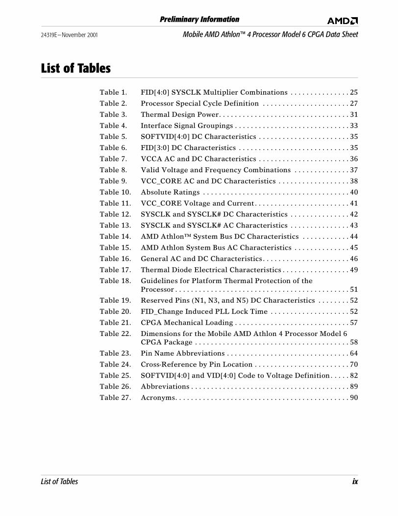
Table 1. FID[4:0] SYSCLK Multiplier Combinations . . . . . . . . . . . . . . . 25
Table 2. Processor Special Cycle Definition . . . . . . . . . . . . . . . . . . . . . . 27
Table 3. Thermal Design Power. . . . . . . . . . . . . . . . . . . . . . . . . . . . . . . . . 31
Table 4. Interface Signal Groupings . . . . . . . . . . . . . . . . . . . . . . . . . . . . . 33
Table 5. SOFTVID[4:0] DC Characteristics . . . . . . . . . . . . . . . . . . . . . . . 35
Table 6. FID[3:0] DC Characteristics . . . . . . . . . . . . . . . . . . . . . . . . . . . . 35
Table 7. VCCA AC and DC Characteristics . . . . . . . . . . . . . . . . . . . . . . . 36
Table 8. Valid Voltage and Frequency Combinations . . . . . . . . . . . . . . 37
Table 9. VCC_CORE AC and DC Characteristics . . . . . . . . . . . . . . . . . . 38
Table 10. Absolute Ratings . . . . . . . . . . . . . . . . . . . . . . . . . . . . . . . . . . . . . 40
Table 11. VCC_CORE Voltage and Current. . . . . . . . . . . . . . . . . . . . . . . . 41
Table 12. SYSCLK and SYSCLK# DC Characteristics . . . . . . . . . . . . . . . 42
Table 13. SYSCLK and SYSCLK# AC Characteristics . . . . . . . . . . . . . . . 43
Table 14. AMD Athlon™ System Bus DC Characteristics . . . . . . . . . . . . 44
Table 15. AMD Athlon System Bus AC Characteristics . . . . . . . . . . . . . . 45
Table 16. General AC and DC Characteristics . . . . . . . . . . . . . . . . . . . . . . 46
Table 17. Thermal Diode Electrical Characteristics . . . . . . . . . . . . . . . . . 49
Table 18. Guidelines for Platform Thermal Protection of the Processor . . . . . . . . . . . . . . . . . . . . . . . . . . . . . . . . . . . . . . . . . . . . 51
Table 19. Reserved Pins (N1, N3, and N5) DC Characteristics . . . . . . . . 52
Table 20. FID_Change Induced PLL Lock Time . . . . . . . . . . . . . . . . . . . . 52
Table 21. CPGA Mechanical Loading . . . . . . . . . . . . . . . . . . . . . . . . . . . . . 57
Table 22. Dimensions for the Mobile AMD Athlon 4 Processor Model 6CPGA Package . . . . . . . . . . . . . . . . . . . . . . . . . . . . . . . . . . . . . . . 58
Table 23. Pin Name Abbreviations . . . . . . . . . . . . . . . . . . . . . . . . . . . . . . . 64
Table 24. Cross-Reference by Pin Location . . . . . . . . . . . . . . . . . . . . . . . . 70
Table 25. SOFTVID[4:0] and VID[4:0] Code to Voltage Definition . . . . . 82
Table 26. Abbreviations . . . . . . . . . . . . . . . . . . . . . . . . . . . . . . . . . . . . . . . . 89
Table 27. Acronyms. . . . . . . . . . . . . . . . . . . . . . . . . . . . . . . . . . . . . . . . . . . . 90
List of Tables ix

Mobile AMD Athlon™ 4 Processor Model 6 CPGA Data Sheet 24319E—November 2001
Preliminary Information
x List of Tables

24319E—November 2001 Mobile AMD Athlon™ 4 Processor Model 6 CPGA Data Sheet
Preliminary Information
Revision History
Date Rev Description
November 2001 E Revised “Thermal Protection Characterization” on page 50.
November 2001 D
Added the 1200 MHz speed grade with a new –50 mV transient (both AC and DC)requirement and a 1.35 V maximum DC voltage. This change effects:
• Table 9, “VCC_CORE AC and DC Characteristics,” on page 38• Table 11, “VCC_CORE Voltage and Current,” on page 41
• Figure 17, “OPN Example for the Mobile AMD Athlon™ 4 Processor Model 6” onpage 85
Revised Table 16, “General AC and DC Characteristics,” on page 46 to add FID validitytiming requirement.
Added “Open Drain Test Circuit” on page 48 and Figure 12, “General ATE Open Drain TestCircuit” on page 48.
Added “Thermal Protection Characterization” on page 50 and Table 18, “Guidelines forPlatform Thermal Protection of the Processor,” on page 51.
Revised notes 7 and 8 of “Power-Up Timing Requirements” on page 54.
Revised Table 22, “Dimensions for the Mobile AMD Athlon™ 4 Processor Model 6 CPGAPackage,” on page 58.
October 2001 C Revised Table 9, “VCC_CORE AC and DC Characteristics,” on page 38, and Figure 9,
“VCC_CORE Voltage Waveform” on page 39.
August 2001 B
Updated Chapter 1, “Overview” on page 1.
Updated Figure 13, “Signal Relationship Requirements During Power-Up Sequence” onpage 53 and supporting text in “Power-Up Timing Requirements” on page 54.
Corrected Table 22, “Dimensions for the Mobile AMD Athlon™ 4 Processor Model 6CPGA Package,” on page 58 and Figure 14 on page 59.
July 2001 A Initial Public Release
Revision History xi

Mobile AMD Athlon™ 4 Processor Model 6 CPGA Data Sheet 24319E—November 2001
Preliminary Information
xii Revision History

24319E—November 2001 Mobile AMD Athlon™ 4 Processor Model 6 CPGA Data Sheet
Preliminary Information
1 Overview
The Mobile AMD Athlon™ 4 Processor Model 6 powers the next generation of high-performance notebook computing platforms,
delivering an unprecedented mobile computing experience.
The mobile AMD Athlon™ 4 processor model 6 providesextremely high-performance processing power for cutting-edgesoftware applications, including digital content creation, digitalphoto editing, digital video, image compression, video encodingfor streaming over the internet, soft DVD, commercial 3Dmodeling, workstation-class Computer-Aided Design (CAD),commercial desktop publishing, and speech recognition. It alsooffers the scalability and “peace-of-mind” reliability that ITmanagers and business users require for enterprise computing.
This processor incorporates AMD PowerNow!™ technology, anadvanced power management solution that providesperformance-on-demand while extending battery life.
This processor features a seventh-generation microarchitecturewith an integrated L2 cache that supports the growingprocessor and system bandwidth requirements of emergingsoftware, graphics, I/O, and memory technologies. Thehigh-speed execution core of the processor includes multiplex86 instruction decoders, a dual-ported 128-Kbyte splitlevel-one (L1) cache, a 256-Kbyte L2 integrated cache, threeindependent integer pipelines, three address calculationpipelines, and a fully pipelined, out-of-order, floating-pointengine.
The processor microarchitecture incorporates 3DNow!™professional technology, a h igh -per formance c achearchitecture, and the 200-MHz, 1.6 Gigabyte per secondAMD Athlon system bus. The AMD Athlon system buscombines the latest technological advances, such aspoint-to-point topology, source-synchronous packet-basedtransfers, and low-voltage signaling. This combination providesan extremely powerful, scalable bus available for any AMDprocessor-based x86 processor. The AMD Athlon system buscombines the latest technological advances, such aspoint-to-point topology, source-synchronous packet-basedtransfers, and low-voltage signaling, to provide a powerful,scalable bus architecture
Chapter 1 Overview 1

Mobile AMD Athlon™ 4 Processor Model 6 CPGA Data Sheet 24319E—November 2001
Preliminary Information
This processor is binary-compatible with existing x86 softwareand backwards compatible with applications optimized forenhanced 3DNow!, MMX™, and SSE instructions. Using a dataformat and Single-Instruction Multiple-Data (SIMD) operationsbased on the MMX instruction model, the processor canproduce as many as four, 32-bit, single-precision floating-pointresults per clock cycle, resulting in peak performance of 4.8Gflops at 1200 MHz (fully scalable). The 3DNow! professionaltechnology implemented in the processor includes new integermultimedia instructions and software-directed data movementinstructions for optimizing such applications as digital contentcreation and streaming video for the internet, as well as newinstruct ions for Dig i ta l S ignal Process ing(DSP)/communications applications.
1.1 Processor Microarchitecture Summary
The following features summarize the mobile AMD Athlon 4processor model 6 microarchitecture:
High performance and power saving modes specifically fornotebook designs with AMD PowerNow! technology
The industry's first nine-issue, superpipelined, superscalarx86 processor microarchitecture designed for high clockfrequencies
Multiple x86 instruction decoders
Fully pipelined floating-point execution unit that executesall x87 (floating-point), MMX, SSE, and 3DNow! professionaltechnology instructions
Three out-of-order, superscalar, pipelined integer units
Three out-of-order, superscalar, pipelined addresscalculation units
A 72-entry instruction control unit
Advanced dynamic branch prediction
3DNow! professional technology with new instructions toenable improved integer math calculations for speech orvideo encoding and improved data movement for internetplug-ins and other streaming applications
A 200-MHz AMD Athlon system bus (scalable beyond 400MHz) enabling leading-edge system bandwidth for datamovement-intensive applications
High-performance cache architecture featuring anintegrated 128-Kbyte L1 cache and a 256-Kbyte L2 cache
2 Overview Chapter 1

24319E—November 2001 Mobile AMD Athlon™ 4 Processor Model 6 CPGA Data Sheet
Preliminary Information
The mobile AMD Athlon 4 processor model 6 deliversoutstanding system performance in a cost-effective, low-profilePGA package. Figure 1 shows a typical mobile AMD Athlon 4processor model 6 system block diagram.
Figure 1. Typical Mobile AMD Athlon™ 4 Processor Model 6 System Block Diagram
SDRAM or DDR
Memory Bus
AGP
PCI Bus
LAN PC Card
ISA or LPC
USB
Dual EIDE
Docking Controller
Modem / Audio
Programmable Voltage Regulator
Thermal Monitor
Battery Super I/O
Embedded Controller
Mobile
AMD Athlon™ 4 Processor Model 6
System Controller (Northbridge)
Peripheral Bus Controller
(Southbridge)
AM D Athlon systembus
AGP Bus
Chapter 1 Overview 3

Mobile AMD Athlon™ 4 Processor Model 6 CPGA Data Sheet 24319E—November 2001
Preliminary Information
4 Overview Chapter 1

24319E—November 2001 Mobile AMD Athlon™ 4 Processor Model 6 CPGA Data Sheet
Preliminary Information
2 Interface Signals
2.1 Overview
The AMD Athlon™ system bus architecture is designed todeliver excellent data movement bandwidth for next-generation x86 platforms as well as the high-performancerequired by enterprise-class application software. The systembus architecture consists of three high-speed channels (aunidirectional processor request channel, a unidirectionalprobe channel, and a 72-bit bidirectional data channel),source-synchronous clocking, and a packet-based protocol. Inaddition, the system bus supports several control, clock, andlegacy signals. The interface signals use an impedancecontrolled push-pull, low-voltage, swing-signaling technologycontained within the Socket A socket.
For more information, see “AMD Athlon™ System Bus Signals”on page 6, Chapter 10, “Pin Descriptions” on page 61, and theAMD Athlon™ and AMD Duron™ Processor System BusSpecification, order# 21902.
2.2 Signaling Technology
The AMD Athlon system bus uses a low-voltage, swing-signalingtechnology, that has been enhanced to provide larger noisemargins, reduced ringing, and variable voltage levels. Thesignals are push-pull and impedance compensated. The signalinputs use differential receivers that require a referencevoltage (VREF). The reference signal is used by the receivers todetermine if a signal is asserted or deasserted by the source.Termination resistors are not needed because the driver isimpedance-matched to the motherboard and a high impedancereflection is used at the receiver to bring the signal past theinput threshold.
For more information about pins and signals, see Chapter 10,“Pin Descriptions” on page 61.
Chapter 2 Interface Signals 5

Mobile AMD Athlon™ 4 Processor Model 6 CPGA Data Sheet 24319E—November 2001
Preliminary Information
2.3 Push-Pull (PP) Drivers
The mobile AMD Athlon 4 processor model 6 supportsPush-Pull (PP) drivers. The system logic configures theprocessor with the configuration parameter called SysPushPull(1=PP). The impedance of the PP drivers is set to match theimpedance of the motherboard by two external resistorsconnected to the ZN and ZP pins.
See “ZN and ZP Pins” on page 83 for more information.
2.4 AMD Athlon™ System Bus Signals
The AMD Athlon system bus is a clock-forwarded, point-to-point interface with the following three point-to-point channels:
A 13-bit unidirectional output address/command channel
A 13-bit unidirectional input address/command channel
A 72-bit bidirectional data channel
For more information, see Chapter 7, “Electrical Data” on page33 and the AMD Athlon™ and AMD Duron™ Processor SystemBus Specification, order# 21902.
6 Interface Signals Chapter 2

24319E—November 2001 Mobile AMD Athlon™ 4 Processor Model 6 CPGA Data Sheet
Preliminary Information
3 Logic Symbol Diagram
Figure 2 is the mobile AMD Athlon™ 4 processor model 6 logicsymbol diagram, showing the logical grouping of the input andoutput signals.
Figure 2. Logic Symbol Diagram
SDATA[63:0]#
SDATAINCLK[3:0]#
SDATAOUTCLK[3:0]#
Data
SADDIN[14:2]#SADDINCLK#
Probe/SysCMD
SADDOUT[14:2]#SADDOUTCLK#
VID[4:0]
FID[3:0]
A20M#
CLKFWDRSTCONNECT
COREFB COREFB#
FERR IGNNE# INIT# INTR NMI
PROCRDY
PWROK
RESET#
SFILLVALID#
SMI#
STPCLK#
SYSCLK#SYSCLK
Clock
VoltageControl
FrequencyControl
LegacyRequest
Mobile AMD Athlon™ 4
Processor Model 6
SDATAINVALID#
SDATAOUTVALID#
Power
and InitializationManagement Thermal
DiodeTHERMDA
THERMDC
FLUSH#
SOFTVID[4:0]
Chapter 3 Logic Symbol Diagram 7

Mobile AMD Athlon™ 4 Processor Model 6 CPGA Data Sheet 24319E—November 2001
Preliminary Information
8 Logic Symbol Diagram Chapter 3

24319E—November 2001 Mobile AMD Athlon™ 4 Processor Model 6 CPGA Data Sheet
Preliminary Information
4 Power Management
This chapter describes the power management features of themobile AMD Athlon™ 4 processor model 6. The powermanagement features of the processor are compliant with theACPI 1 .0b and ACPI 2 .0 speci f icat ions and supportAMD PowerNow!™ technology.
4.1 Power Management States
The mobile AMD Athlon™ 4 processor model 6 has a variety ofoperating states that are designed to support different powermanagement goals. In addition to the standard operating state,the processor supports low-power Halt and Stop Grant statesand the FID_Change state. These states are used by AdvancedConfiguration and Power Interface (ACPI) enabled operatingsystems, for processor power management. AMD PowerNow!software is used to control processor performance states withoperating systems that do not support ACPI 2.0-definedprocessor performance state control.
Figure 3 on page 10 shows the power management states of theprocessor. The f igure includes the ACPI “Cx” namingconvention for these states.
Chapter 4 Power Management 9

Mobile AMD Athlon™ 4 Processor Model 6 CPGA Data Sheet 24319E—November 2001
Preliminary Information
Figure 3. Mobile AMD Athlon™ 4 Processor Model 6 Power Management States
The following sections provide an overview of the powermanageme nt states . Fo r more de tai l s , refer to theAMD Athlon™ and AMD Duron™ Processor System BusSpecification, order# 21902.
Note: In all power management states that the processor ispowered, the system must not stop the system clock(SYSCLK/SYSCLK#) to the processor.
Working State The Working state is the state in which the processor isexecuting instructions.
Halt State When the processor executes the HLT instruction, the processorenters the Halt state and issues a Halt special cycle to theAMD Athlon system bus. The processor only enters the lowpower state dictated by the CLK_Ctl MSR if the system
C1Halt
C0Working4
Execute HLT
SMI#, INTR, NMI, INIT#, RESET#
Incoming Probe
Probe Serviced
STPCLK# asserted
STPCLK# asserted 2
STPCLK# deasserted 3
C2Stop Grant
Cache Snoopable
Incoming Probe
Probe ServicedProbeState1
STPCLK#deasserted
(Read PLVL2 registeror throttling)
C3/S1Stop Grant
Cache Not Snoopable Sleep
STPCLK# asserted
STPCLK# deasserted
FID_Change
Write to FidVidCtl MSR
SIP Stream and System Bus Connect
Note: The AMD AthlonTM System Bus is connected during the following states:1) The Probe state 2) During transitions between the Halt state and the C2 Stop Grant state3) During transitions between the C2 Stop Grant state and the Halt state4) C0 Working state
Software transitionsHardware transitions
Legend
10 Power Management Chapter 4

24319E—November 2001 Mobile AMD Athlon™ 4 Processor Model 6 CPGA Data Sheet
Preliminary Information
controller (Northbridge) disconnects the AMD Athlon systembus in response to the Halt special cycle.
If STPCLK# is asserted, the processor will exit the Halt stateand enter the Stop Grant state. The processor will initiate asystem bus connect, if it is disconnected, then issue a StopGrant special cycle. When STPCLK# is deasserted, theprocessor will exit the Stop Grant state and re-enter the Haltstate. The processor will issue a Halt special cycle whenre-entering the Halt state.
The Halt state is exited when the processor detects theassertion of INIT#, INTR, NMI, RESET#, or SMI#. When theHalt state is exited the processor will initiate an AMD Athlonsystem bus connect if it is disconnected.
Stop Grant States The processor enters the Stop Grant state upon recognition ofassertion of STPCLK# input. After entering the Stop Grantstate, the processor issues a Stop Grant special bus cycle on theAMD Athlon system bus. The processor is not in a low-powerstate at this time, because the AMD Athlon system bus is stillconnected. After the Northbridge disconnects the AMD Athlonsystem bus in response to the Stop Grant special bus cycle, theprocessor enters a low-power state dictated by the CLK_CtlMSR. If the Northbridge needs to probe the processor duringthe Stop Grant state while the system bus is disconnected, itmust first connect the system bus. Connecting the system busplaces the processor into the higher power probe state. Afterthe Northbridge has completed all probes of the processor, theNorthbridge must disconnect the AMD Athlon system busagain so that the processor can return to the low-power state.During the Stop Grant states, the processor latches INIT#,INTR, NMI, and SMI#, if they are asserted.
The Stop Grant state is exited upon the deassertion ofSTPCLK# or the assertion of RESET#. When STPCLK# isdeasserted, the processor will initiate a connect of theAMD Athlon system bus if it is disconnected. After theprocessor enters the Working state, any pending interrupts arerecognized and serviced and the processor resumes executionat the instruction boundary where STPCLK# was initiallyrecognized. If RESET# is sampled asserted during the StopGrant state, the processor exits the Stop Grant state and thereset process begins.
Chapter 4 Power Management 11

Mobile AMD Athlon™ 4 Processor Model 6 CPGA Data Sheet 24319E—November 2001
Preliminary Information
There are two mechanisms for asserting STPCLK#—hardwareand software.
The Southbridge can force STPCLK# assertion for throttling toprotect the processor from exceeding its maximum casetemperature. This is accomplished by asserting the THERM#input to the Southbridge. Throttling asserts STPCLK# for apercentage of a predefined throttling period: STPCLK# isrepetitively asserted and deasserted until THERM# isdeasserted.
Software can force the processor into the Stop Grant state byaccessing ACPI-defined registers typically located in theSouthbridge.
The operating system places the processor into the C2 StopGrant state by reading the P_LVL2 register in the Southbridge.
If an ACPI Thermal Zone is defined for the processor, theoperating system can initiate throttling with STPCLK# usingthe ACPI defined P_CNT register in the Southbridge. TheNorthbridge connects the AMD Athlon system bus, and theprocessor enters the Probe state to service cache snoops duringStop Grant for C2 or throttling.
In C2, probes are allowed, as shown in Figure 3 on page 10.
The operating system places the processor into the C3 StopGrant state by reading the P_LVL3 register in the Southbridge.In C3, the operating system and Northbridge hardware enforcea policy that prevents the processor from being probed. TheSouthbridge will deassert STPCLK# and bring the processorout of the C3 Stop Grant state if a bus master request, interrupt,or any other enabled resume event occurs.
The Stop Grant state is also entered for the S1, Powered OnSuspend, system sleep state based on a write to the SLP_TYPand SLP_EN fields in the ACPI-defined Power Management 1control register in the Southbridge. During the S1 sleep state,system software ensures no bus master or probe activity occurs.The Southbridge deasserts STPCLK# and brings the processorout of the S1 Stop Grant state when any enabled resume eventoccurs.
12 Power Management Chapter 4

24319E—November 2001 Mobile AMD Athlon™ 4 Processor Model 6 CPGA Data Sheet
Preliminary Information
Probe State The Probe state is entered when the Northbridge connects theAMD Athlon system bus to probe the processor (for example, tosnoop the processor caches) when the processor is in the Halt orStop Grant state. When in the Probe state, the processorresponds to a probe cycle in the same manner as when it is inthe Working state. When the probe has been serviced, theprocessor returns to the same state as when it entered theProbe state (Halt or Stop Grant state). When probe activity iscompleted the processor only returns to a low-power state afterthe Northbridge disconnects the AMD Athlon system bus again.
FID_Change State The FID_Change State is part of the AMD Athlon system busFID_Change Protocol. During the FID_Change state theFrequency Identification (FID[4:0]) code that determines thecore frequency of the processor and Voltage Identification(VID[4:0]) driven on the SOFTVID[4:0] pins are transitioned tochange the core frequency and core voltage of the processor.
Note: The FID[3:0] pins of the processor do not transition as partof the FID_Change protocol.
Processor Performance States and the FID_Change Protocol
The FID_Change protocol is used by AMD PowerNow! softwareto transition the processor from one performance state toanother. The FID_Change protocol is also used for ACPI2.0-compliant processor performance state control.
Processor performance states are combinations of processorcore voltage and core frequency. Processor performance statesare used in mobile systems to optimize the power consumptionof the processor (and therefore battery powered run-time)based upon processor utilization.
Table 8, “Valid Voltage and Frequency Combinations,” onpage 37 specifies the valid voltage and frequency combinationssupported by the processor based upon the maximum corefrequency and the maximum nominal core voltage supported bythe processor.
The core frequency is determined by a 5-bit Frequency ID (FID)code. The core voltage is determined by a 5-bit Voltage ID (VID)code.
Before PWROK is asserted to the processor, the VID[4:0]outputs of the processor dictate the core voltage level of theprocessor.
Chapter 4 Power Management 13

Mobile AMD Athlon™ 4 Processor Model 6 CPGA Data Sheet 24319E—November 2001
Preliminary Information
After PWROK is asserted, the core voltage of the processoris dictated by the SOFTVID[4:0] outputs. The SOFTVID[4:0]outputs of the processor are not driven to a deterministicvalue until after PWROK is asserted to the processor. Themotherboard therefore must provide a ‘VID Multiplexer’ todrive the VID[4:0] outputs to the DC/DC converter for thecore voltage of the processor before PWROK is asserted anddrive the SOFTVID[4:0] outputs to the DC to DC converterafter PWROK is asserted.
The FID[3:0] signals are valid after PWROK is asserted. Thechipset must not sample the FID[3:0] signals until theybecome valid.
After RESET# is deasserted, the FID[3:0] outputs are notused to transmit FID information for subsequent softwarecontrolled changes in the operating frequency of theprocessor.
Processor performance state transitions are required tooccur as two separate transitions. The order of thesetransitions depends on whether the transition is to a higheror lower performance state. When transitioning from a lowerperformance state to a higher performance state the orderof the transitions is:
1. The FID_Change protocol is used to transition to thehigher voltage, while keeping the frequency fixed atthe current setting.
2. The FID_Change protocol is then used to transition tothe higher frequency, while keeping the voltage fixedat the higher setting.
When transitioning from a high performance state to alower performance state the order of the transitions is:
1. The FID_Change protocol is used to transition to thelower frequency, while keeping the voltage fixed at itscurrent setting.
2. The FID_Change protocol is then used to transition tothe lower voltage, while keeping the frequency fixed atthe lower setting.
The processor provides two MSRs to support theFID_Change protocol: the FidVidCtl MSR and theFidVidStatus MSR. For a definition of these MSRs and theiruse, refer to the Mobile AMD Athlon™ and MobileAMD Duron™ Processor BIOS Developer Application Note,order# 24141.
14 Power Management Chapter 4

24319E—November 2001 Mobile AMD Athlon™ 4 Processor Model 6 CPGA Data Sheet
Preliminary Information
FID_Change Protocol Description By Example:
Note: In any FID_Change transition only the core voltage or corefrequency of the processor is transitioned. Two FID_Changetransitions are required to transition the voltage andfrequency to a valid performance state. When the voltage isbeing transitioned, the frequency is held constant bytransitioning to the same FID[3:0] as the current FIDreported in the FidVidStatus MSR.
System software determines that a change in processorperformance state is required.
System software executes a WRMSR instruction to write tothe FidVidCtl MSR to dictate:
• The new VID[4:0] code that will be driven to the DC/DCconverter from the SOFTVID[4:0] outputs of theprocessor that selects the new core voltage level.
• The new FID[4:0] code that will be used by the processorto dictate its new operating frequency.
• A Stop Grant Timout Count (SGTC)[19:0] value thatdetermines how many SYSCLK/SYSCLK# 100-MHz clockperiods the processor will remain in the FID_Changestate. This time accounts for the time that it takes for thePLL of the processor to lock to the new core frequencyand the time that it takes for the core voltage of theprocessor to ramp to the new value.
• The FIDCHGRATIO bit must be set to 1.
• The VIDC bit must be set to a 1 if the voltage is going tobe changed.
• The FIDC bit must be set to a 1 if the frequency is goingto be changed.
Writing the SGTC field to a non-zero value initiates theFID_Change protocol.
On the instruction boundary that the SGTC field of theFidVidCtl MSR is written to a non-zero value, the processorstops code execution and issues a FID_Change special cycleon the AMD Athlon system bus.
The FID_Change special cycle has a data encoding of0007_0002h that is passed on SDATA[31:0].
SDATA[36:32] contain the new FID[4:0] code during theFID_Change special cycle. The Northbridge is required to
Chapter 4 Power Management 15

Mobile AMD Athlon™ 4 Processor Model 6 CPGA Data Sheet 24319E—November 2001
Preliminary Information
capture this FID[4:0] code when the FID_Change specialcycle is run.
In response to receiving the FID_Change special cycle, theNorthbridge is required to disconnect. The Northbridge willcomplete any in-progress bus cycles and then disable itsarbiter before disconnecting the AMD Athlon system bus sothat it will not initiate a AMD Athlon system bus connectbased on bus master or other activity. The Northbridge mustdisconnect the AMD Athlon system bus or the system willhang because the processor is not executing any operatingsystem or application code and is waiting for theAMD Athlon system bus to disconnect so that it cancontinue with the FID_Change protocol. The Northbridgeinitiates an AMD Athlon system bus disconnect in the usualmanner: it deasserts CONNECT.
The processor allows the disconnect to complete bydeasserting PROCRDY. The Northbridge completes thedisconnect by asserting CLKFWDRST.
Once the AMD Athlon system bus has been disconnected inresponse to a FID_Change special cycle, the Northbridge isnot allowed to initiate a re-connect, the processor isresponsible for the eventual re-connect.
After the AMD Athlon system bus is disconnected, theprocessor enters a low-power state where the clock grid isramped down by a value specified in the CLK_Ctl MSR.
After entering the low-power state, the processor will:
• begin counting down the value that was programmed intothe SGTC field
• drive the new VID[4:0] value on SOFTVID[4:0], causingits core voltage to transition
• drive the new FID[4:0] value to its PLL, causing the PLLto lock to the new core frequency.
When the SGTC count reaches zero, the processor will rampits entire clock grid to full frequency (the PLL is alreadylocked to) and signal that it is ready for the Northbridge totransmit the new SIP (Serial Initialization Protocol) streamassociated with the new processor core operating frequency.The processor signals this by pulsing PROCRDY high andthen low.
The Northbridge responds to this high pulse on PROCRDYby pulsing CLKFWDRST low and then transferring a SIPstream as it does after PROCRDY is deasserted after the
16 Power Management Chapter 4

24319E—November 2001 Mobile AMD Athlon™ 4 Processor Model 6 CPGA Data Sheet
Preliminary Information
SOFTV
deassertion of RESET#. The difference is that the SIPstream that the Northbridge transmits to the processor nowcorresponds to the FID[4:0] that was transmitted onSDATA[36:32] during the FID_Change special cycle.
After the SIP stream is transmitted, the processor initiatesthe AMD Athlon system bus connect sequence by assertingPROCRDY. The Northbridge responds by deassertingCLKFWDRST. The forward clocks are started and theprocessor issues a Connect special cycle.
The AMD Athlon system bus connection causes theprocessor to resume execution of operating system andapplication code at the instruction that follows the WRMSRto the FidVidCtl MSR that started the FID_Change protocoland processor performance state transition.
Figure 4 illustrates the processor SOFTVID transitionduring the AMD Athlon system bus disconnect in responseto a FID_Change special cycle.
Figure 4. SOFTVID Transition During the AMD Athlon™ System Bus Disconnect for FID_Change
1.4 V
CPUCOREVCC1.2 V
ID[4:0] from theprocessor
VID combination that selects 1.2 V
< 100 µµµµs
ProcRdy
Connect
ClkFwdRst
VID combination that selects 1.4 V
The processor core frequency changes and new SOFTVID[4:0] values are driven after the system bus interface disconnect occurs and the processor has entered a low power state. The duration of the disconnect is dictated by software programming the FidVidControl MSR in the processor.
Chapter 4 Power Management 17
Mobile AMD Athlon™ 4 Processor Model 6 CPGA Data Sheet 24319E—November 2001
Preliminary Information
4.2 Connect and Disconnect Protocol
Significant power savings of the processor only occur if theprocessor is disconnected from the system bus by theNorthbridge while in the Halt or Stop Grant state. TheNorthbridge can optionally initiate a bus disconnect upon thereceipt of a Halt or Stop Grant special cycle. The option ofdisconnecting is controlled by an enable bit in the Northbridge.If the Northbridge requires the processor to service a probeafter the system bus has been disconnected, it must firstinitiate a system bus connect.
Connect Protocol In addition to the legacy STPCLK# signal and the Halt and StopGrant special cycles, the AMD Athlon system bus connectprotocol includes the CONNECT, PROCRDY, and CLKFWDRSTsignals and a Connect special cycle.
AMD Athlon system bus disconnects are initiated by theNorthbridge in response to the receipt of a Halt, Stop Grant, orFID_Change special cycle. Reconnect is initiated by theprocessor in response to an interrupt for Halt, STPCLK#deassertion, or completion of a FID_Change transition.Reconnect is initiated by the Northbridge to probe theprocessor.The Northbridge contains BIOS programmableregisters to enable the system bus disconnect in response toHalt and Stop Grant special cycles. When the Northbridgereceives the Halt or Stop Grant special cycle from the processorand, if there are no outstanding probes or data movements, theNorthbridge deasserts CONNECT a minimum of eight SYSCLKperiods after the last command sent to the processor. Theprocessor detects the deassertion of CONNECT on a rising edgeof SYSCLK and deasserts PROCRDY to the Northbridge. Inreturn, the Northbridge asserts CLKFWDRST in anticipation ofreestablishing a connection at some later point.
Note: The Northbridge must disconnect the processor from theAMD Athlon system bus before issuing the Stop Grantspecial cycle to the PCI bus or passing the Stop Grant specialcycle to the Southbridge for systems that connect to theSouthbridge with HyperTransport™ technology.
This note applies to current chipset implementation—alternate chipset implementations that do not require thisare possible.
18 Power Management Chapter 4
24319E—November 2001 Mobile AMD Athlon™ 4 Processor Model 6 CPGA Data Sheet
Preliminary Information
Note: In response to Halt special cycles, the Northbridge passes theHalt special cycle to the PCI bus or Southbridgeimmediately.
The processor can receive an interrupt after it sends a Haltspecial cycle, or STPCLK# deassertion after it sends a StopGrant special cycle to the Northbridge but before thedisconnect actually occurs. In this case, the processor sends theConnect special cycle to the Northbridge, rather thancontinuing with the disconnect sequence. In response to theConnect special cycle, the Northbridge cancels the disconnectrequest.
The system is required to assert the CONNECT signal beforereturning the C-bit for the connect special cycle (assumingCONNECT has been deasserted).
For more information, see the AMD Athlon™ and AMD Duron™Processor System Bus Specification, order# 21902 for thedefinition of the C-bit and the Connect special cycle.
Chapter 4 Power Management 19

Mobile AMD Athlon™ 4 Processor Model 6 CPGA Data Sheet 24319E—November 2001
Preliminary Information
Figure 5 shows STPCLK# assertion resulting in the processor inthe Stop Grant state and the AMD Athlon system busdisconnected.
Figure 5. AMD Athlon™ System Bus Disconnect Sequence in the Stop Grant State
An example of the AMD Athlon system bus disconnectsequence is as follows:
1. The peripheral controller (Southbridge) asserts STPCLK#to place the processor in the Stop Grant state.
2. When the processor recognizes STPCLK# asserted, it entersthe Stop Grant state and then issues a Stop Grant specialcycle.
3. When the special cycle is received by the Northbridge, itdeasserts CONNECT, assuming no probes are pending,initiating a bus disconnect to the processor.
4. The processor responds to the Northbridge by deassertingPROCRDY.
5. The Northbridge asserts CLKFWDRST to complete the busdisconnect sequence.
6. After the processor is disconnected from the bus, theprocessor enters a low-power state. The Northbridge passesthe Stop Grant special cycle along to the Southbridge.
Stop Grant
Stop Grant
STPCLK#
CONNECT
PROCRDY
CLKFWDRST
PCI Bus
AMD Athlon™ System Bus
20 Power Management Chapter 4

24319E—November 2001 Mobile AMD Athlon™ 4 Processor Model 6 CPGA Data Sheet
Preliminary Information
Figure 6 shows the signal sequence of events that takes theprocessor out of the Stop Grant state, connects the processor tothe AMD Athlon system bus, and puts the processor into theWorking state.
Figure 6. Exiting the Stop Grant State and Bus Connect Sequence
The following sequence of events removes the processor fromthe Stop Grant state and connects it to the system bus:
1. The Southbridge deasserts STPCLK#, informing theprocessor of a wake event.
2. When the processor recognizes STPCLK# deassertion, itexits the low-power state and asserts PROCRDY, notifyingthe Northbridge to connect to the bus.
3. The Northbridge asserts CONNECT.
4. The Northbridge deasserts CLKFWDRST, synchronizing theforwarded clocks between the processor and theNorthbridge.
5. The processor issues a Connect special cycle on the systembus and resumes operating system and application codeexecution.
STPCLK#
PROCRDY
CONNECT
CLKFWDRST
Chapter 4 Power Management 21

Mobile AMD Athlon™ 4 Processor Model 6 CPGA Data Sheet 24319E—November 2001
Preliminary Information
Connect State Diagram
Figure 7 and Figure 8 on page 23 describe the Northbridge andprocessor connect state diagrams, respectively.
Figure 7. Northbridge Connect State Diagram
Condition
1 A disconnect is requested and probes are still pending.
2 A disconnect is requested and no probes are pending.
3 A Connect special cycle from the processor.
4 No probes are pending.
5 PROCRDY is deasserted.
6 A probe needs service.
7 PROCRDY is asserted.
8
Three SYSCLK periods after CLKFWDRST is deasserted.
Although reconnected to the system interface, the Northbridge must not issue any non-NOP SysDC commands for a minimum of four SYSCLK periods after deasserting CLKFWDRST.
Action
ADeassert CONNECT eight SYSCLK periodsafter last SysDC sent.
B Assert CLKFWDRST.
C Assert CONNECT.
D Deassert CLKFWDRST.
DisconnectPending
ConnectDisconnectRequested
ReconnectPending
ProbePending 2
Disconnect
ProbePending 1
1
3
2/A
4/A
5/B
3/C
7/D,C
8
6/C 7/D
8
22 Power Management Chapter 4

24319E—November 2001 Mobile AMD Athlon™ 4 Processor Model 6 CPGA Data Sheet
Preliminary Information
Figure 8. Processor Connect State Diagram
Condition
1CONNECT is deasserted by the Northbridge (for a previously sent Halt or Stop Grant special cycle).
2Processor receives a wake-up event and must cancel the disconnect request.
3 Deassert PROCRDY and slow down internal clocks.
4Processor wake-up event or CONNECT asserted by Northbridge.
5 CLKFWDRST is deasserted by the Northbridge.
6Forward clocks start three SYSCLK periods after CLKFWDRST is deasserted.
Action
A CLKFWDRST is asserted by the Northbridge.
B Issue a Connect special cycle.*
CReturn internal clocks to full speed and assertPROCRDY.
* The Connect special cycle is only issued after a processor wake-up event (interrupt or STPCLK# deassertion) occurs. If the AMD Athlon™ processor system bus is connected so the Northbridge can probe the processor, a Connect special cycle is not issued at that time (it is only issued after a subsequent processor wake-up event).
Connect
DisconnectPending
Disconnect
Connect
Pending 1Connect
Pending 2
1
3/A
4/C
5
6/B
2/B
Chapter 4 Power Management 23

Mobile AMD Athlon™ 4 Processor Model 6 CPGA Data Sheet 24319E—November 2001
Preliminary Information
4.3 Clock Control
The processor implements a Clock Control (CLK_Ctl) MSR(address C001_001Bh) that determines the internal clockdivisor when the AMD Athlon system bus is disconnected.
Refer to the AMD Athlon™ and AMD Duron™ Processors BIOS,Software, and Debug Developers Guide, order# 21656, for moredetails on the CLK_Ctl register.
Refer to the Mobile AMD Athlon™ and Mobile AMD Duron™Processor BIOS Developer Application Note, order# 24141, formore details on the CLK_Ctl register.
4.4 SYSCLK Multipliers
The processor provides two mechanisms for communicatingprocessor core operating frequency information to theNorthbridge. These are the processor FID[3:0] outputs and theFID_Change special cycle. The FID[3:0] outputs specify thecore frequency of the processor as a multiple of the 100-MHzinput clock (SYSCLK/SYSCLK#) of the processor.
The FID[3:0] signals are valid after PWROK is asserted. Thechipset must not sample the FID[3:0] signals until they becomevalid.The FID[3:0] outputs of the processor provide processoroperating frequency information that the Northbridge useswhen creating the SIP stream that the Northbridge sends to theprocessor after RESET# is deasserted. The FID[3:0] outputsalways select a 5x SYSCLK multiplier:
FID[3:0] = 0 1 0 0
Software will use the FID_Change protocol to transition theprocessor to the desired performance state.
The FID[3:0] outputs are not used as part of the FID_Changeprotocol and do not change from their RESET# value duringsoftware-controlled processor core frequency transitions.
The FID_Change special cycle is used to communicateprocessor operating frequency information to the Northbridgeduring software-controlled processor core voltage andfrequency (performance state) transitions. The FidVidCtl MSR
24 Power Management Chapter 4

24319E—November 2001 Mobile AMD Athlon™ 4 Processor Model 6 CPGA Data Sheet
Preliminary Information
al lows sof tware to specify a 5 -b it FID value duringsoftware-controlled processor performance state transitions.The additional bit allows transitions to lower SYSCLKmultipliers of 3x to 4x as well as all other SYSCLK multiplierssupported by the processor.
For a description of the FID_Change protocol refer to theearlier section in this chapter.
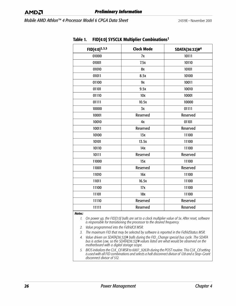
Table 1 lists the FID[4:0] SYSCLK multiplier codes for theprocessor used by software to dictate the core frequency of theprocessor and the 5-bit value driven on SDATA[36:32]# by theprocessor during the FID_Change special bus cycle.
Note: Only clock multipliers associated with operating frequenciesspecified in the “Electrical Data” chapter are valid for thisprocessor.
Note: Software distinguishes the speed grade of the processor byreading the MFID field of the FidVidStatus MSR.
Table 1. FID[4:0] SYSCLK Multiplier Combinations1
FID[4:0]2,3,5 Clock Mode SDATA[36:32]#4
00000 11x 11111
00001 11.5x 11110
00010 12x 11101
00011 12.5x 11100
00100 5x 11011
00101 5.5x 11010
00110 6x 11001
00111 6.5x 11000Notes:
1. On power up, the FID[3:0] balls are set to a clock multiplier value of 5x. After reset, software is responsible for transitioning the processor to the desired frequency.
2. Value programmed into the FidVidCtl MSR. 3. The maximum FID that may be selected by software is reported in the FidVidStatus MSR.4. Value driven on SDATA[36:32]# balls during the FID_Change special bus cycle. The SDATA
bus is active Low, so the SDATA[36:32]# values listed are what would be observed on the motherboard with a digital storage scope.
5. BIOS initializes the CLK_Ctl MSR to 6007_9263h during the POST routine. This CLK_Ctl setting is used with all FID combinations and selects a halt disconnect divisor of 128 and a Stop–Grant disconnect divisor of 512.
Chapter 4 Power Management 25
Mobile AMD Athlon™ 4 Processor Model 6 CPGA Data Sheet 24319E—November 2001
Preliminary Information
01000 7x 10111
01001 7.5x 10110
01010 8x 10101
01011 8.5x 10100
01100 9x 10011
01101 9.5x 10010
01110 10x 10001
01111 10.5x 10000
10000 3x 01111
10001 Reserved Reserved
10010 4x 01101
10011 Reserved Reserved
10100 13x 11100
10101 13.5x 11100
10110 14x 11100
10111 Reserved Reserved
11000 15x 11100
11001 Reserved Reserved
11010 16x 11100
11011 16.5x 11100
11100 17x 11100
11101 18x 11100
11110 Reserved Reserved
11111 Reserved Reserved
Table 1. FID[4:0] SYSCLK Multiplier Combinations1
FID[4:0]2,3,5 Clock Mode SDATA[36:32]#4
Notes:1. On power up, the FID[3:0] balls are set to a clock multiplier value of 5x. After reset, software
is responsible for transitioning the processor to the desired frequency. 2. Value programmed into the FidVidCtl MSR. 3. The maximum FID that may be selected by software is reported in the FidVidStatus MSR.4. Value driven on SDATA[36:32]# balls during the FID_Change special bus cycle. The SDATA
bus is active Low, so the SDATA[36:32]# values listed are what would be observed on the motherboard with a digital storage scope.
5. BIOS initializes the CLK_Ctl MSR to 6007_9263h during the POST routine. This CLK_Ctl setting is used with all FID combinations and selects a halt disconnect divisor of 128 and a Stop–Grant disconnect divisor of 512.
26 Power Management Chapter 4
24319E—November 2001 Mobile AMD Athlon™ 4 Processor Model 6 CPGA Data Sheet
Preliminary Information
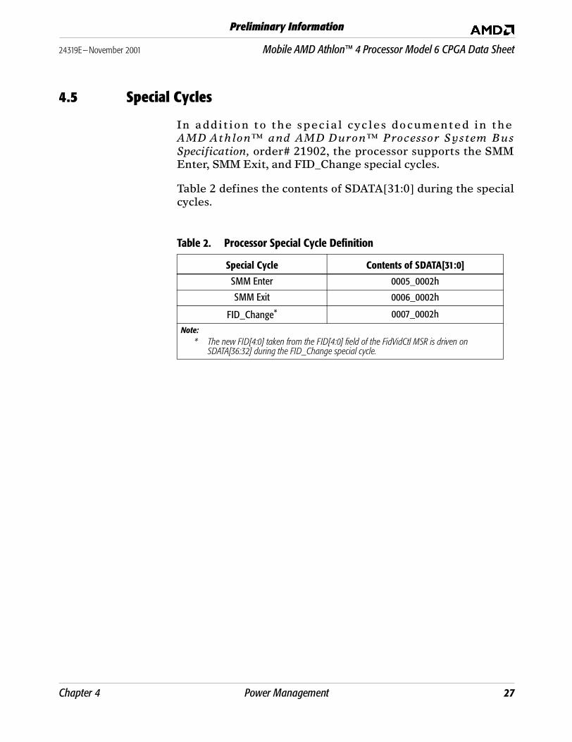
4.5 Special Cycles
In addition to the special cycles documented in theAMD Athlon™ and AMD Duron™ Processor System BusSpecification, order# 21902, the processor supports the SMMEnter, SMM Exit, and FID_Change special cycles.
Table 2 defines the contents of SDATA[31:0] during the specialcycles.
Table 2. Processor Special Cycle Definition
Special Cycle Contents of SDATA[31:0]
SMM Enter 0005_0002h
SMM Exit 0006_0002h
FID_Change* 0007_0002h
Note:* The new FID[4:0] taken from the FID[4:0] field of the FidVidCtl MSR is driven on
SDATA[36:32] during the FID_Change special cycle.
Chapter 4 Power Management 27

Mobile AMD Athlon™ 4 Processor Model 6 CPGA Data Sheet 24319E—November 2001
Preliminary Information
28 Power Management Chapter 4

24319E—November 2001 Mobile AMD Athlon™ 4 Processor Model 6 CPGA Data Sheet
Preliminary Information
5 CPUID Support
The mobile AMD Athlon™ 4 processor model 6 version andfeature set recognition can be performed through the use of theCPUID instruction, that provides complete information aboutthe processor—vendor, type, name, etc., and its capabilities.Software can make use of this information to accurately tunethe system for maximum performance and benefit to users.
For information on the use of the CPUID instruction see:
AMD Athlon™ Processor Recognition Application NoteAddendum, order# 21922
For information on additions to the CPUID instructionfunctionality specific to the mobile AMD Athlon™ 4 processormodel 6 see:
Mobile AMD Athlon™ and Mobile AMD Duron™ ProcessorBIOS Developer Application Note, order# 24141
For information about the CPUID features supported by themobile AMD Athlon 4 processor model 6, refer to the followingdocuments:
AMD Processor Recognition Application Note, order# 20734
AMD Athlon™ Processor Recognition Application NoteAddendum, order# 21922
AMD Athlon™ Processors BIOS Developers Application Note,order# 21656
Chapter 5 CPUID Support 29

Mobile AMD Athlon™ 4 Processor Model 6 CPGA Data Sheet 24319E—November 2001
Preliminary Information
30 CPUID Support Chapter 5

24319E—November 2001 Mobile AMD Athlon™ 4 Processor Model 6 CPGA Data Sheet
Preliminary Information
6 Thermal Design
The Mobile AMD Athlon™ 4 Processor Model 6 provides adiode that can be used in conjunction with an externaltemperature sensor to determine the die temperature of theprocessor.
The diode anode (THERMDA) and cathode (THERMDC) areavailable as pins on the processor.
Refer to “Thermal Diode Characteristics” on page 49 and“THDA and THDC Pins” on page 83 for more details.
For information about the usage of this diode and thermaldesign, including layout and airflow considerations, see theMobile System Thermal Design Guidelines, order# 24383.
Table 3 shows the thermal design power.
Table 3. Thermal Design Power
Frequency(MHz) Nominal Voltage
Thermal DesignPower1,2
850 1.40 V 22 W
900 1.40 V 24 W
950 1.40 V 24 W
1000 1.40 V 25 W
1100 1.40 V 25 W
1200 1.35 V 25 W
Notes:1. Thermal design power represents the maximum sustained power dissipated while executing
publicly-available software or instruction sequences under normal system operation at nominal VCC_CORE. Thermal solutions must monitor the temperature of the processor to prevent the processor from exceeding its maximum die temperature.
2. Specified through characterization for a die temperature of 95°C.
Chapter 6 Thermal Design 31

Mobile AMD Athlon™ 4 Processor Model 6 CPGA Data Sheet 24319E—November 2001
Preliminary Information
32 Thermal Design Chapter 6

24319E—November 2001 Mobile AMD Athlon™ 4 Processor Model 6 CPGA Data Sheet
Preliminary Information
7 Electrical Data
7.1 Conventions
The conventions used in this chapter are as follows:
Current specified as being sourced by the processor isnegative.
Current specified as being sunk by the processor is positive.
7.2 Interface Signal Groupings
The electrical data in this chapter is presented separately foreach signal group.
Table 4 defines each group and the signals contained in eachgroup.
Table 4. Interface Signal Groupings
Signal Group Signals Notes
Power VID[4:0], SOFTVID[4:0], VCCA, VCC_CORE, COREFB, COREFB#
See “Absolute Ratings” on page 40, “Soft Voltage Identification (SOFTVID[4:0])” on page 35, “VCCA AC and DC Characteristics” on page 36, “VCC_CORE AC and DC Characteristics” on page 38, “COREFB and COREFB# Pins” on page 78, “SOFTVID[4:0] and VID[4:0] Pins” on page 81, and “VCCA Pin” on page 83.
Frequency FID[3:0]See “Frequency Identification (FID[3:0])” on page 35 and “FID[3:0] Pins” on page 79.
System ClocksSYSCLK, SYSCLK# (Tied to CLKIN/CLKIN# and RSTCLK/RSTCLK#), PLLBYPASSCLK, PLLBYPASSCLK#,
See “SYSCLK and SYSCLK# AC and DC Characteristics” on page 42, “SYSCLK and SYSCLK#” on page 83, and “PLL Bypass and Test Pins” on page 80.
Chapter 7 Electrical Data 33
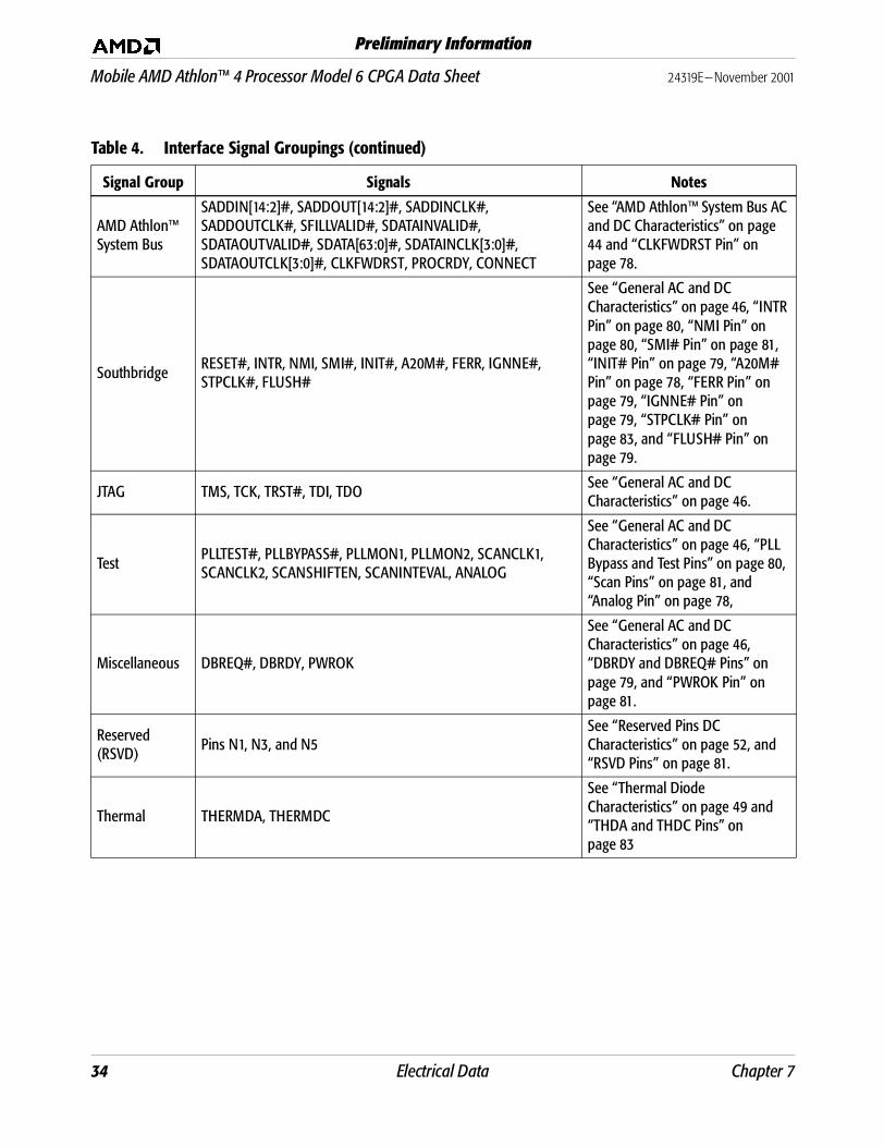
Mobile AMD Athlon™ 4 Processor Model 6 CPGA Data Sheet 24319E—November 2001
Preliminary Information
AMD Athlon™ System Bus
SADDIN[14:2]#, SADDOUT[14:2]#, SADDINCLK#, SADDOUTCLK#, SFILLVALID#, SDATAINVALID#, SDATAOUTVALID#, SDATA[63:0]#, SDATAINCLK[3:0]#, SDATAOUTCLK[3:0]#, CLKFWDRST, PROCRDY, CONNECT
See “AMD Athlon™ System Bus AC and DC Characteristics” on page 44 and “CLKFWDRST Pin” on page 78.
SouthbridgeRESET#, INTR, NMI, SMI#, INIT#, A20M#, FERR, IGNNE#, STPCLK#, FLUSH#
See “General AC and DC Characteristics” on page 46, “INTR Pin” on page 80, “NMI Pin” on page 80, “SMI# Pin” on page 81, “INIT# Pin” on page 79, “A20M# Pin” on page 78, “FERR Pin” on page 79, “IGNNE# Pin” on page 79, “STPCLK# Pin” on page 83, and “FLUSH# Pin” on page 79.
JTAG TMS, TCK, TRST#, TDI, TDOSee “General AC and DC Characteristics” on page 46.
TestPLLTEST#, PLLBYPASS#, PLLMON1, PLLMON2, SCANCLK1, SCANCLK2, SCANSHIFTEN, SCANINTEVAL, ANALOG
See “General AC and DC Characteristics” on page 46, “PLL Bypass and Test Pins” on page 80, “Scan Pins” on page 81, and “Analog Pin” on page 78,
Miscellaneous DBREQ#, DBRDY, PWROK
See “General AC and DC Characteristics” on page 46, “DBRDY and DBREQ# Pins” on page 79, and “PWROK Pin” on page 81.
Reserved (RSVD)
Pins N1, N3, and N5See “Reserved Pins DC Characteristics” on page 52, and “RSVD Pins” on page 81.
Thermal THERMDA, THERMDC
See “Thermal Diode Characteristics” on page 49 and “THDA and THDC Pins” on page 83
Table 4. Interface Signal Groupings (continued)
Signal Group Signals Notes
34 Electrical Data Chapter 7

24319E—November 2001 Mobile AMD Athlon™ 4 Processor Model 6 CPGA Data Sheet
Preliminary Information
7.3 Soft Voltage Identification (SOFTVID[4:0])
Table 5 shows the SOFTVID[4:0] DC Characteristics. For moreinformation, see “SOFTVID[4:0] and VID[4:0] Pins” onpage 81.
7.4 Frequency Identification (FID[3:0])
Table 6 shows the FID[3:0] DC characteristics. For moreinformation, see “FID[3:0] Pins” on page 79.
Table 5. SOFTVID[4:0] DC Characteristics
Parameter Description Min Max
IOL Output Current Low 16 mA
SOFTVID_VOH SOFTVID[4:0] Output High Voltage – 2.625V *
Note:* The SOFTVID pins must not be pulled above this voltage by an external pullup resistor.
Table 6. FID[3:0] DC Characteristics
Parameter Description Min Max
IOL Output Current Low 16 mA
VOH Output High Voltage – 2.625 V *
Note:* The FID pins must not be pulled above this voltage by an external pullup resistor.
Chapter 7 Electrical Data 35

Mobile AMD Athlon™ 4 Processor Model 6 CPGA Data Sheet 24319E—November 2001
Preliminary Information
7.5 VCCA AC and DC Characteristics
Table 7 shows the AC and DC characteristics for VCCA. Formore information, see “VCCA Pin” on page 83.
7.6 Decoupling
See the AMD Athlon™ Processor-Based Motherboard DesignGuide, order# 24363, or contact your local AMD office forinformation about the decoupling required on the motherboardfor use with the mobile AMD Athlon™ 4 processor model 6.
Table 7. VCCA AC and DC Characteristics
Symbol Parameter Min Nominal Max Units Notes
VVCCA VCCA Pin Voltage 2.25 2.5 2.75 V 1
IVCCA VCCA Pin Current 0 50 mA/GHz 2
Notes:1. Minimum and Maximum voltages are absolute. No transients below minimum nor above maximum voltages are permitted.2. Measured at 2.5 V.
36 Electrical Data Chapter 7

24319E—November 2001 Mobile AMD Athlon™ 4 Processor Model 6 CPGA Data Sheet
Preliminary Information
7.7 Valid Voltage and Frequency Combinations
Table 8 specifies the valid voltage and frequency combinationsthat this processor is characterized to operate. The MaximumFrequency column corresponds to the rated frequency of theprocessor. The Maximum FID (MFID) field in the FidVidStatusMSR is used by software to determine the maximum frequencyof the processor. Each row in the table shows the maximumfrequency allowable at the voltage specified in each column.
“Power Management States” on page 9 describes howAMD PowerNow!™ software uses th is information toimplement processor performance states.
Table 8. Valid Voltage and Frequency Combinations
Maximum FrequencyVCC_CORE_NOM Voltage
1.400 V 1.350 V 1.300 V 1.250 V 1.200 V
850 MHz 850 MHz 700 MHz 600 MHz 500 MHz ≤ 500 MHz
900 MHz 900 MHz 700 MHz 600 MHz 500 MHz ≤ 500 MHz
950 MHz 950 MHz 800 MHz 700 MHz 600 MHz ≤ 500 MHz
1000 MHz 1000 MHz 800 MHz 700 MHz 600 MHz ≤ 500 MHz
1100 MHz 1100 MHz 900 MHz 800 MHz 700 MHz ≤ 600 MHz
1200 MHz N/A 1200 MHz 1000 MHz 900 MHz ≤ 800 MHzNotes:
1. All voltages listed are nominal. See Figure 9 on page 39 for AC and DC transient voltage tolerances.2. The “≤“ symbol indicates that the BIOS vendor can use any performance state equal to or less than the specified frequency at that
given voltage. For example, “≤ 800 MHz” means that the BIOS may use 800 MHz, 700 MHz, 600 MHz, 500 MHz, 400 MHz, or 300 MHz provided that the chipset and system support the chosen processor operating frequencies.
3. The maximum processor die temperature is 95º C for all voltage and frequency combinations.
Chapter 7 Electrical Data 37

Mobile AMD Athlon™ 4 Processor Model 6 CPGA Data Sheet 24319E—November 2001
Preliminary Information
7.8 VCC_CORE AC and DC Characteristics
Table 9 shows the AC and DC characteristics for VCC_CORE.For more information, see Table 24, “Cross-Reference by PinLocation,” on page 70 and Figure 9 on page 39.
Table 9. VCC_CORE AC and DC Characteristics
Symbol Parameter Limit in Working State2 Units
VCC_CORE_DC_MAX Maximum static voltage above VCC_CORE_NOM1 100 mV
VCC_CORE_DC_MIN Maximum static voltage below VCC_CORE_NOM1 –50 mV
VCC_CORE_AC_MAX Maximum excursion above VCC_CORE_NOM1 150 mV
VCC_CORE_AC_MINMaximum excursion below VCC_CORE_NOM
1, 3 for processors with a maximum frequency of 1200 MHz
–50 mV
VCC_CORE_AC_MINMaximum excursion below VCC_CORE_NOM
1, 3 for all other processors
–100 mV
tMAX_AC Maximum excursion time for AC transients 10 µs
tMIN_AC Negative excursion time for AC transients 5 µs
Notes:1. VCC_CORE nominal values are shown in Table 8, “Valid Voltage and Frequency Combinations,” on page 37. 2. All voltage measurements are taken differentially at the COREFB/COREFB# pins.3. Absolute minimum allowable VCC_CORE voltage, including all transients, is 1.10 V.
38 Electrical Data Chapter 7
24319E—November 2001 Mobile AMD Athlon™ 4 Processor Model 6 CPGA Data Sheet
Preliminary Information
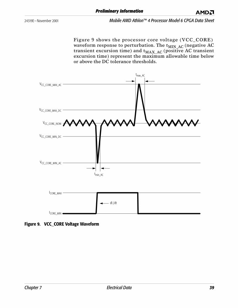
Figure 9 shows the processor core voltage (VCC_CORE)waveform response to perturbation. The tMIN_AC (negative ACtransient excursion time) and tMAX_AC (positive AC transientexcursion time) represent the maximum allowable time belowor above the DC tolerance thresholds.
Figure 9. VCC_CORE Voltage Waveform
tmin_AC
VCC_CORE_MAX_AC
tmax_AC
VCC_CORE_MAX_DC
VCC_CORE_NOM
VCC_CORE_MIN_DC
VCC_CORE_MIN_AC
ICORE_MIN
ICORE_MAX
dI /dt
Chapter 7 Electrical Data 39

Mobile AMD Athlon™ 4 Processor Model 6 CPGA Data Sheet 24319E—November 2001
Preliminary Information
7.9 Absolute Ratings
Do not subject the processor to conditions that exceed theabsolute ratings listed in Table 10, as such conditions mayadversely affect long-term reliability or result in functionaldamage.
Table 10. Absolute Ratings
Parameter Description Min Max
VCC_CORE Mobile AMD Athlon™ 4 Processor Model 6 core supply –0.5 V VCC_CORE Max + 0.5 V
VCCA Mobile AMD Athlon 4 Processor Model 6 PLL supply –0.5 V VCCA Max + 0.5 V
VPIN Voltage on any signal pin –0.5 V VCC_CORE Max + 0.5 V
TSTORAGE Storage temperature of processor –40ºC 100ºC
40 Electrical Data Chapter 7

24319E—November 2001 Mobile AMD Athlon™ 4 Processor Model 6 CPGA Data Sheet
Preliminary Information
7.10 VCC_CORE Voltage and Current
Table 11 shows the voltage and current of the processor duringnormal and reduced power states.
Table 11. VCC_CORE Voltage and Current
Frequency(MHz) Voltage
Maximum ICC (Power Supply Current)
Die Temperature Notes
850
1.40 V
15.71 A
95°C
900 17.14 A
950 17.14 A
1000 17.90 A
1100 17.90 A
1200 1.35 V 18.50 A
Halt/Stop Grant C2
1.20 V
2.00 A 1, 2, 3
Stop Grant C2 1.07 A50°C
1, 2, 3, 4
Stop Grant C3/S1 0.80 A 1, 2, 3, 4Notes:
1. See also Figure 3, “Mobile AMD Athlon™ 4 Processor Model 6 Power Management States” on page 10.2. The maximum Stop Grant currents are absolute worst case currents for parts that may yield from the worst case corner
of the process, and are not representative of the typical Stop Grant current that is currently about one–third of the maximum specified current.
3. These currents occur when the AMD Athlon system bus is disconnected and a low power ratio of 1/512 is applied to the core clock grid of the processor. A low power ratio of 1/512 is dictated by a value of 6007_9263h programmed into the Clock Control (CLK_Ctl) MSR,.
4. The Stop Grant current consumption is characterized and not tested.
Chapter 7 Electrical Data 41

Mobile AMD Athlon™ 4 Processor Model 6 CPGA Data Sheet 24319E—November 2001
Preliminary Information
7.11 SYSCLK and SYSCLK# AC and DC Characteristics
Table 12 shows the DC characteristics of the SYSCLK andSYSCLK# differential clocks. The SYSCLK signal representsCLKIN and RSTCLK tied together while the SYSCLK# signalrepresents CLKIN# and RSTCLK# tied together.
Figure 10 shows the DC characteristics of the SYSCLK andSYSCLK# signals.
Figure 10. SYSCLK and SYSCLK# Differential Clock Signals
Table 12. SYSCLK and SYSCLK# DC Characteristics
Symbol Description Min Max Units
VThreshold-DC Crossing before transition is detected (DC) 400 mV
VThreshold-AC Crossing before transition is detected (AC) 450 mV
ILEAK_P Leakage current through P-channel pullup to VCC_CORE –250 µA
ILEAK_N Leakage current through N-channel pulldown to VSS (Ground) 250 µA
VCROSS Differential signal crossoverVCC_CORE/2
±100mV
CPIN Capacitance * 4 12 pF
Note:* The following processor inputs have twice the listed capacitance because they connect to two input pads—SYSCLK and SYSCLK#.
SYSCLK connects to CLKIN/RSTCLK. SYSCLK# connects to CLKIN#/RSTCLK#.
VCROSS VThreshold-DC = 400 mV VThreshold-AC = 450 mV
42 Electrical Data Chapter 7

24319E—November 2001 Mobile AMD Athlon™ 4 Processor Model 6 CPGA Data Sheet
Preliminary Information
Table 13 shows the mobile AMD Athlon 4 processor model 6SYSCLK/SYSCLK# differential clock AC characteristics.
Figure 11 shows a sample waveform.
Figure 11. SYSCLK Waveform
Table 13. SYSCLK and SYSCLK# AC Characteristics
Symbol Description Min Max Units Notes
Clock Frequency 50 100 MHz
Duty Cycle 30% 70% –
t1 Period 10 ns 1, 2
t2 High Time 1.8 ns
t3 Low Time 1.8 ns
t4 Fall Time 2 ns
t5 Rise Time 2 ns
Period Stability ± 300 psNotes:
1. Circuitry driving the SYSCLK and SYSCLK# inputs must exhibit a suitably low closed-loop jitter bandwidth to allow the PLL to track the jitter. The –20 dB attenuation point, as measured into a 10-pF or 20-pF load, must be less than 500 kHz.
2. Circuitry driving the SYSCLK and SYSCLK# inputs may purposely alter the SYSCLK and SYSCLK# period (spread spectrum clock generators). In no cases can the period violate the minimum specification above. SYSCLK and SYSCLK# inputs may vary from 100% of the specified period to 99% of the specified period at a maximum rate of 100 kHz.
t5
VCROSS
t2
t3
t4
t1
VThreshold-AC
Chapter 7 Electrical Data 43

Mobile AMD Athlon™ 4 Processor Model 6 CPGA Data Sheet 24319E—November 2001
Preliminary Information
7.12 AMD Athlon™ System Bus AC and DC CharacteristicsTable 14 shows the DC characteristics of the AMD Athlonsystem bus.
Table 14. AMD Athlon™ System Bus DC Characteristics
Symbol Parameter Condition Min Max Units Notes
VREF DC Input Reference Voltage(0.5 x VCC_CORE)
–50(0.5 x VCC_CORE)
+50mV 1
IVREF_LEAK_P VREF Tristate Leakage Pullup VIN=VREFNominal –100 µA
IVREF_LEAK_NVREF Tristate Leakage Pulldown
VIN=VREFNominal +100 µA
VIH Input High Voltage VREF + 200 VCC_CORE + 500 mV
VIL Input Low Voltage –500 VREF – 200 mV
VOH Output High Voltage IOUT = –200 µA 0.85*VCC_CORE VCC_CORE+500 mV 2
VOL Output Low Voltage IOUT = 1 mA –500 400 mV 2
ILEAK_P Tristate Leakage PullupVIN= VSS (Ground)
–250 µA
ILEAK_N Tristate Leakage PulldownVIN= VCC_CORE Nominal
+250 µA
CIN Input Pin Capacitance 4 12 pF
Notes:1. VREF
– VREF is nominally set by a (1%) resistor divider from VCC_CORE.– The suggested divider resistor values are 100 ohms over 100 ohms to produce a divisor of 0.50.– Example: VCC_CORE = 1.4 V, VREF = 750 mV (1.4 x 0.50). – Peak-to-Peak AC noise on VREF (AC) should not exceed 2% of VREF (DC).
2. Specified at T = 95°C and VCC_CORE.
44 Electrical Data Chapter 7

24319E—November 2001 Mobile AMD Athlon™ 4 Processor Model 6 CPGA Data Sheet
Preliminary Information
The AC characteristics of the AMD Athlon system bus areshown in Table 15. The parameters are grouped based on thesource or destination of the signals involved.
Table 15. AMD Athlon™ System Bus AC Characteristics
Group Symbol Parameter Min Max Units Notes
All SignalsTRISE Output Rise Slew Rate 1 3 V/ns 1
TFALL Output Fall Slew Rate 1 3 V/ns 1
Forward Clocks
TSKEW-SAMEEDGEOutput skew with respect to the same clock edge
– 385 ps 2
TSKEW-DIFFEDGEOutput skew with respect to a different clock edge
– 770 ps 2
TSU Input Data Setup Time 300 ps 3
THD Input Data Hold Time 300 ps 3
CIN Capacitance on input Clocks 4 12 pF
COUT Capacitance on output Clocks 4 12 pF
Sync
TVAL RSTCLK to Output Valid 250 2000 ps 4, 5
TSU Setup to RSTCLK 500 ps 4, 6
THD Hold from RSTCLK 1000 ps 4, 6
Notes:1. Rise and fall time ranges are guidelines over which the I/O has been characterized.2. TSKEW-SAMEEDGE is the maximum skew within a clock forwarded group between any two signals or between any signal and its
forward clock, as measured at the package, with respect to the same clock edge.TSKEW-DIFFEDGE is the maximum skew within a clock forwarded group between any two signals or between any signal and its forward clock, as measured at the package, with respect to different clock edges.
3. Input SU and HD times are with respect to the appropriate Clock Forward Group input clock.4. The synchronous signals include PROCRDY, CONNECT, and CLKFWDRST.5. TVAL is RSTCLK rising edge to output valid for PROCRDY. Test Load is 25 pF.6. TSU is setup of CONNECT/CLKFWDRST to rising edge of RSTCLK. THD is hold of CONNECT/CLKFWDRST from rising edge of
RSTCLK.
Chapter 7 Electrical Data 45

Mobile AMD Athlon™ 4 Processor Model 6 CPGA Data Sheet 24319E—November 2001
Preliminary Information
7.13 General AC and DC Characteristics
Table 16 shows the mobile AMD Athlon 4 processor model 6 ACand DC characteristics of the Southbridge, JTAG, test, andmiscellaneous pins.
Table 16. General AC and DC Characteristics
Symbol Parameter Description Condition Min Max Units Notes
VIH Input High Voltage(VCC_CORE/2) +
200mVVCC_CORE Max V 1, 2
VIL Input Low Voltage –300 350 mV 1, 2
VOH Output High Voltage VCC_CORE – 400VCC_CORE +
300mV
VOL Output Low Voltage –300 400 mV
ILEAK_P Tristate Leakage Pullup VIN= VSS (Ground) –250 µA
ILEAK_N Tristate Leakage PulldownVIN= VCC_CORE
Nominal250 µA
IOH Output High Current –16 mA 3
IOL Output Low Current 16 mA 3
TSU Sync Input Setup Time 2.0 ns 4, 5
THD Sync Input Hold Time 0.0 ps 4, 5
TDELAYOutput Delay with respect to RSTCLK
0.0 6.1 ns 5
Notes:1. Characterized across DC supply voltage range.2. Values specified at nominal VCC_CORE. Scale parameters between VCC_CORE Min and VCC_CORE Max.3. IOL and IOH are measured at VOL maximum and VOH minimum, respectively.4. Synchronous inputs/outputs are specified with respect to RSTCLK and RSTCK# at the pins.5. These are aggregate numbers. 6. Edge rates indicate the range over which inputs were characterized.7. In asynchronous operation, the signal must persist for this time to enable capture.8. This value assumes RSTCLK frequency is 10 ns ==> TBIT = 2*fRST.9. The approximate value for standard case in normal mode operation.10. This value is dependent on RSTCLK frequency, divisors, Low Power mode, and core frequency.11. Reassertions of the signal within this time are not guaranteed to be seen by the core.12. This value assumes that the skew between RSTCLK and K7CLKOUT is much less than one phase.13. This value assumes RSTCLK and K7CLKOUT are running at the same frequency, though the processor is capable of other
configurations.14. Time to valid is for any open drain pins. See requirements 7 and 8 in Chapter 8, “Power–Up Timing Requirements,“ for more
information.
46 Electrical Data Chapter 7

24319E—November 2001 Mobile AMD Athlon™ 4 Processor Model 6 CPGA Data Sheet
Preliminary Information
TBIT Input Time to Acquire 20.0 ns 7, 8
TRPT Input Time to Reacquire 40.0 ns 9–13
TRISE Signal Rise Time 1.0 3.0 V/ns 6
TFALL Signal Fall Time 1.0 3.0 V/ns 6
CPIN Pin Capacitance 4 12 pF
TVALID Time to data valid 100 ns 14
Table 16. General AC and DC Characteristics (continued)
Symbol Parameter Description Condition Min Max Units Notes
Notes:1. Characterized across DC supply voltage range.2. Values specified at nominal VCC_CORE. Scale parameters between VCC_CORE Min and VCC_CORE Max.3. IOL and IOH are measured at VOL maximum and VOH minimum, respectively.4. Synchronous inputs/outputs are specified with respect to RSTCLK and RSTCK# at the pins.5. These are aggregate numbers. 6. Edge rates indicate the range over which inputs were characterized.7. In asynchronous operation, the signal must persist for this time to enable capture.8. This value assumes RSTCLK frequency is 10 ns ==> TBIT = 2*fRST.9. The approximate value for standard case in normal mode operation.10. This value is dependent on RSTCLK frequency, divisors, Low Power mode, and core frequency.11. Reassertions of the signal within this time are not guaranteed to be seen by the core.12. This value assumes that the skew between RSTCLK and K7CLKOUT is much less than one phase.13. This value assumes RSTCLK and K7CLKOUT are running at the same frequency, though the processor is capable of other
configurations.14. Time to valid is for any open drain pins. See requirements 7 and 8 in Chapter 8, “Power–Up Timing Requirements,“ for more
information.
Chapter 7 Electrical Data 47

Mobile AMD Athlon™ 4 Processor Model 6 CPGA Data Sheet 24319E—November 2001
Preliminary Information
7.14 Open Drain Test Circuit
Figure 12 is a test circuit that may be used on Automated TestEquipment (ATE) to test for validity on open drain pins.
Refer to Table 16, “General AC and DC Characteristics,” onpage 46 for timing requirements.
Figure 12. General ATE Open Drain Test Circuit
Open Drain Pin
VTermination1
50 Ω ±3%
IOL = Output Current2
Notes:1. VTermination = 1.2 V for VID and FID pins
2. IOL = –16 mA for VID and FID pins
48 Electrical Data Chapter 7

24319E—November 2001 Mobile AMD Athlon™ 4 Processor Model 6 CPGA Data Sheet
Preliminary Information
7.15 Thermal Diode Characteristics
Thermal Diode Electrical Characteristics. Table 17 shows the mobileAMD Athlon 4 processor model 6 electrical characteristics ofthe on-die thermal diode.
Table 17. Thermal Diode Electrical Characteristics
Symbol Parameter Description Min Nom Max Units Notes
Ifw Forward bias current 5 300 µA 1
n Diode ideality factor 1.002 1.008 1.016 2, 3, 4, 5Notes:
1. The sourcing current should always be used in forward bias only.2. Characterized at 95°C with a forward bias current pair of 10 µA and 100 µA.3. Not 100% tested. Specified by design and limited characterization.4. The diode ideality factor, n, is a correction factor to the ideal diode equation.
For the following equations, use the following variables and constants:n Diode ideality factork Boltzmann constantq Electron charge constantT Diode temperature (Kelvin)VBE Voltage from base to emitterIC Collector currentIS Saturation currentN Ratio of collector currents
The equation for VBE is:
By sourcing two currents and using the above equation, a difference in base emitter voltage can be found that leads to the following equation for temperature:
5. If a different sourcing current pair is used other than 10 µA and 100 µA, the following equation should be used to correct the temperature. Subtract this offset from the temperature measured by the temperature sensor.
For the following equations, use the following variables and constants:Ihigh High sourcing currentIlow Low sourcing current
Toffset (in °C) can be found using the following equation:
VBEnkT
q---------
IC
IS-----
ln⋅=
T∆VBE
n N( )lnkq---⋅ ⋅
-----------------------------=
Toffset 6.0 104⋅( )
Ihigh Ilow–( )Ihigh
Ilow-----------
ln
--------------------------------⋅ 2.34–=
Chapter 7 Electrical Data 49

Preliminary Information
Mobile AMD Athlon™ 4 Processor Model 6 CPGA Data Sheet 24319E—November 2001
Thermal Protection Characterization. The following section describesparameters relating to thermal protection. The implementationof thermal control circuitry to control processor temperature isleft to the manufacturer to determine how to implement.
Thermal limits in motherboard design are necessary to protectthe processor from thermal damage. TSHUTDOWN is thetemperature for thermal protection circuitry to initiateshutdown of the processor. TSD_DELAY is the maximum timeallowed from the detection of the over-temperature condition toprocessor shutdown to prevent thermal damage to theprocessor.
Systems that do not implement thermal protection circuitry orthat do not react within the time specified by TSD_DELAY cancause thermal damage to the processor during the unlikelyevents of fan failure or powering up the processor without aheat-sink. The processor relies on thermal circuitry on themotherboard to turn off the regulated core voltage to theprocessor in response to a thermal shutdown event.
Thermal protection circuitry reference designs and thermalsolution guidelines are found in the following documents:
AMD Athlon™ Processor-Based Motherboard Design Guide,order# 24363
Thermal Diode Monitoring Circuits, order# 25658
AMD Thermal, Mechanical, and Chassis Cooling Design Guide,order# 23794
http://www1.amd.com/products/athlon/thermals
Mobile specific thermal documentation:
Measuring Processor and system Power in a Mobile System,order# 24353
Mobile System Thermal Design Guide, order# 24383
Measuring Temperature on AMD Athlon™ and AMD Duron™Pin Grid Array Processors with and without an On-Die ThermalDiode, order#24228
50 Electrical Data Chapter 7

24319E—November 2001 Mobile AMD Athlon™ 4 Processor Model 6 CPGA Data Sheet
Preliminary Information
Table 18 shows the TSHUTDOWN and TSD_DELAY specificationsfor circuitry in motherboard design necessary for thermalprotection of the processor.
Table 18. Guidelines for Platform Thermal Protection of the Processor
Symbol Parameter Description Max Units Notes
TSHUTDOWN Thermal diode shutdown temperature for processor protection 125 °C 1, 2, 3
TSD_DELAYMaximum allowed time from TSHUTDOWN detection to processor shutdown
500 ms 1, 3
Notes:1. The thermal diode is not 100% tested, it is specified by design and limited characterization.2. The thermal diode is capable of responding to thermal events of 40°C/s or faster.3. The mobile AMD Athlon™ 4 processor model 6 provides a thermal diode for measuring die temperature of the processor. The
processor relies on thermal circuitry on the motherboard to turn off the regulated core voltage to the processor in response to a thermal shutdown event. Refer to Thermal Diode Monitoring Circuits, order# 25658, for thermal protection circuitry designs.
Chapter 7 Electrical Data 51

Mobile AMD Athlon™ 4 Processor Model 6 CPGA Data Sheet 24319E—November 2001
Preliminary Information
7.16 Reserved Pins DC Characteristics
Table 19 shows the DC characteristics of the Reserved (RSVD)pins.
7.17 FID_Change Induced PLL Lock Time
Table 20 shows the time required for the PLL of the processor tolock at the new frequency specified in a FID_Change transition.
Software must program the SGTC field of the FidVidCtl MSR toproduce a FID_Change duration equal to or greater than theFID_Change induced PLL lock time.
For more information about the FID_Change protocol, see“Power Management States” on page 9.
Table 19. Reserved Pins (N1, N3, and N5) DC Characteristics
Symbol Parameter Description Min Max Units Note
ILEAK_P Tristate Leakage Pullup –250 µA *
ILEAK_N Tristate Leakage Pulldown 250 µA *
Note:* Measured at 2.5V
Table 20. FID_Change Induced PLL Lock Time
Parameter Description Max Units
FID_Change Induced PLL Lock Time 50 µs
52 Electrical Data Chapter 7

24319E—November 2001 Mobile AMD Athlon™ 4 Processor Model 6 CPGA Data Sheet
Preliminary Information
8 Signal and Power-Up Requirements
This chapter describes the mobile AMD Athlon™ 4 processormodel 6 power-up requirements during system power-up andwarm resets.
8.1 Power-Up Requirements
Signal Sequence and Timing Description
Figure 13 shows the relationship between key signals in thesystem during a power-up sequence. This figure details therequirements of the processor.
Figure 13. Signal Relationship Requirements During Power-Up Sequence
3.3 V Supply
VCCA (2.5 V)(for PLL)
RESET#
VCC_CORE(Processor Core)
NB_RESET#
PWROK
System Clock
2
1
3
4
5
6
FID[3:0]
7 8
Warm reset condition
Notes:
1. Figure 13 represents several signals generically by using names not necessarily consistent withany pin lists or schematics.
2. Requirements 1–8 in Figure 13 are described in “Power-Up Timing Requirements” on page 54.
Chapter 8 Signal and Power-Up Requirements 53

Mobile AMD Athlon™ 4 Processor Model 6 CPGA Data Sheet 24319E—November 2001
Preliminary Information
Power-Up Timing Requirements. The signal timing requirements areas follows:
1. RESET# must be asserted before PWROK is asserted.The mobile AMD Athlon™ 4 processor model 6 does not setthe correct clock multiplier if PWROK is asserted prior to aRESET# assertion. It is recommended that RESET# beasserted at least 10 nanoseconds prior to the assertion ofPWROK.In practice, Southbridges will assert RESET# millisecondsbefore PWROK is deasserted.
2. All motherboard voltage planes must be withinspecification before PWROK is asserted.
PWROK is an output of the voltage regulation circuit on themotherboard. PWROK indicates that VCC_CORE and allother voltage planes in the system are within specification.
The motherboard is required to delay PWROK assertion fora minimum of 3 milliseconds from the 3.3 V supply beingwithin specification. This ensures that the system clock(SYSCLK/SYSCLK#) is operating within specification whenPWROK is asserted.
The processor core voltage, VCC_CORE, must be withinspecification before PWROK is asserted as dictated by theVID[4:0] pins strapped on the processor package. BeforePWROK assertion, the processor is clocked by a ringoscillator. Before PWROK is asserted, the SOFTVID[4:0]outputs of the processor are not driven to a deterministicvalue. The processor drives the SOFTVID[4:0] outputs tothe same value as dictated by the VID[4:0] pins within 20nanoseconds of PWROK assertion.
The processor PLL is powered by VCCA. The processor PLLdoes not lock if VCCA is not high enough for the processorlogic to switch for some period before PWROK is asserted.VCCA must be within specification at least 5 microsecondsbefore PWROK is asserted.
In practice VCCA, VCC_CORE, and all other voltage planesmust be within specification for several milliseconds beforePWROK is asserted.
After PWROK is asserted, the processor PLL locks to itsoperational frequency.
3. The system clock (SYSCLK/SYSCLK#) must be runningbefore PWROK is asserted.
54 Signal and Power-Up Requirements Chapter 8

24319E—November 2001 Mobile AMD Athlon™ 4 Processor Model 6 CPGA Data Sheet
Preliminary Information
When PWROK is asserted, the processor switches fromdriving the internal processor clock grid from the ringoscillator to driving from the PLL. The reference systemclock must be valid at this time. The system clocks aredesigned to be running after 3.3 V has been withinspecification for 3 milliseconds.
4. PWROK assertion to deassertion of RESET#
The duration of RESET# assertion during cold boots isintended to satisfy the time it takes for the PLL to lock witha less than 1 ns phase error. The processor PLL begins torun after PWROK is asserted and the internal clock grid isswitched from the ring oscillator to the PLL. The PLL locktime may take from hundreds of nanoseconds to tens ofmicroseconds. It is recommended that the minimum timebetween PWROK assertion to the deassertion of RESET# beat least 1.0 milliseconds. Southbridges enforce a delay of1.5 to 2.0 milliseconds between PWRGD (Southbridgeversion of PWROK) assertion and NB_RESET# deassertion.
5. PWROK must be monotonic and meet the timingrequirements as defined in “General AC and DCCharacteristics” on page 46. The processor should notswitch between the ring oscillator and the PLL after theinitial assertion of PWROK.
6. NB_RESET# must be asserted (causing CONNECT to alsoassert) before RESET# is deasserted. In practice allSouthbridges enforce this requirement.
If NB_RESET# does not assert until after RESET# hasdeasserted, the processor misinterprets the CONNECTassertion (due to NB_RESET# being asserted) as thebeginning of the SIP transfer. There must be sufficientoverlap in the resets to ensure that CONNECT is sampledasserted by the processor before RESET# is deasserted.
7. The FID[3:0] signals are valid within 100 ns after PWROK isasserted. The chipset must not sample the FID[3:0] signalsuntil they become valid. Refer to the AMD Athlon™Processor Motherboard Design Guide, order# 24363, for thespecific implementation and additional circuitry required.
8. The FID[3:0] signals become valid within 100 ns afterRESET# is asserted. Refer to the AMD Athlon™ ProcessorMotherboard Design Guide, order# 24363, for the specificimplementation and additional circuitry required.
See “Serial Initialization Packet (SIP) Protocol” on page 56 formore information.
Chapter 8 Signal and Power-Up Requirements 55

Mobile AMD Athlon™ 4 Processor Model 6 CPGA Data Sheet 24319E—November 2001
Preliminary Information
Clock Multiplier Selection (FID[3:0])
The chipset samples the FID[3:0] signals in a chipset-specificmanner from the processor and uses this information todetermine the correct Serial Initialization Packet (SIP). Thechipset then sends the SIP information to the processor forconfiguration of the AMD Athlon system bus for the clockmultiplier that determines the processor frequency indicatedby the FID[3:0] code. The SIP is sent to the processor using theSIP protocol. This protocol uses the PROCRDY, CONNECT, andCLKFWDRST signals, that are synchronous to SYSCLK.
For more information, see “FID[3:0] Pins” on page 79.
Serial Initialization Packet (SIP) Protocol. Refer to AMD Athlon™ andAMD Duron™ Processor System Bus Specification, order# 21902for details of the SIP protocol.
8.2 Processor Warm Reset Requirements
Mobile AMD Athlon™ 4 Processor Model 6 and Northbridge Reset Pins
RESET# cannot be asserted to the processor without also beingasserted to the Northbridge. RESET# to the Northbridge is thesame as PCI RESET#. The minimum assertion for PCI RESET#is one millisecond. Southbridges enforce a minimum assertionof RESET# for the processor, Northbridge, and PCI of 1.5 to 2.0milliseconds.
56 Signal and Power-Up Requirements Chapter 8

24319E—November 2001 Mobile AMD Athlon™ 4 Processor Model 6 CPGA Data Sheet
Preliminary Information
9 Mechanical Data
9.1 Introduction
The Mobile AMD Athlon™ 4 Processor Model 6 connects to themotherboard through a PGA socket named Socket A. For moreinformation, see the AMD Athlon™ Processor Based MotherboardDesign Guide, order# 24363.
9.2 Die Loading
The processor die on the CPGA package is exposed at the top ofthe package. This is done to facilitate heat transfer from the dieto the heat sink. It is critical that the mechanical loading of theheat sink does not exceed the limits shown in Table 21. Anyheat sink design should avoid loads on corners and edges of die.The CPGA package has compliant pads that serve to bringsurfaces in planar contact.
Table 21. CPGA Mechanical Loading1
Location Dynamic (MAX) Static (MAX) Units Note
Die Surface 100 30 lbf 2
Die Edge 10 10 lbf 3Notes:
1. Tool–assisted zero insertion force sockets should be designed such that no load is placed on the ceramic substrate of the package.
2. Load specified for coplanar contact to die surface.3. Load defined for a surface at no more than a two degree angle of inclination to die surface.
Chapter 9 Mechanical Data 57

Mobile AMD Athlon™ 4 Processor Model 6 CPGA Data Sheet 24319E—November 2001
Preliminary Information
9.3 Package Dimensions
Figure 14 on page 59 shows a diagram and notes for the mobileAMD Athlon 4 processor model 6 CPGA package. Table 22provides the dimensions in millimeters assigned to the lettersand symbols shown in the Figure 14 diagram.
Table 22. Dimensions for the Mobile AMD Athlon™ 4 Processor Model 6 CPGA Package
Letter or Symbol
Minimum Dimension1
Maximum Dimension1
Letter or Symbol
Minimum Dimension1
Maximum Dimension1
D/E 49.27 49.78 E9 1.66 1.96
D1/E1 45.72 BSC G/H – 4.50
D2 11.698 REF A 2.24 REF
D3 3.30 3.60 A1 1.27 1.53
D4 11.84 12.39 A2 0.80 0.88
D5 11.84 12.39 A3 0.116 –
D6 6.11 6.66 A4 – 1.90
D7 10.85 11.40 φP – 6.60
D8 3.05 3.35 φb 0.43 0.50
E2 11.01 REF φb1 1.40 REF
E3 2.35 2.65 S 1.435 2.375
E4 7.25 7.80 L 3.05 3.31
E5 7.25 7.80 M 37
E6 9.86 10.41 N 453
E7 9.86 10.41 e 1.27 BSC
E8 15.89 16.14 e1 2.54 BSCNote:
1. Dimensions are given in millimeters.
58 Mechanical Data Chapter 9

24319E—November 2001 Mobile AMD Athlon™ 4 Processor Model 6 CPGA Data Sheet
Preliminary Information
Figure 14. Mobile AMD Athlon™ 4 Processor Model 6 CPGA Package
Chapter 9 Mechanical Data 59

Mobile AMD Athlon™ 4 Processor Model 6 CPGA Data Sheet 24319E—November 2001
Preliminary Information
60 Mechanical Data Chapter 9

24319E—November 2001 Mobile AMD Athlon™ 4 Processor Model 6 CPGA Data Sheet
Preliminary Information
10 Pin Descriptions
10.1 Pin Diagram and Pin Name Abbreviations
Figure 15 on page 62 shows the Ceramic Pin Grid Array (CPGA)for the Mobile AMD Athlon™ 4 Processor Model 6. Becausesome of the pin names are too long to fit in the grid, they areabbreviated. Table 23 on page 64 lists all the pins inalphabetical order by pin name, along with the abbreviationwhere necessary.
Chapter 10 Pin Descriptions 61

Mobile AMD Athlon™ 4 Processor Model 6 CPGA Data Sheet 24319E—November 2001
Preliminary Information
12
34
56
78
910
1112
1314
1516
1718
192
021
22
23
24
25
26
27
28
29
30
313
23
33
435
36
37
ASA
O#12
SAO#
5SA
O#3
SD#5
5SD
#61
SD#5
3SD
#63
SD#6
2NC
SD#5
7SD
#39
SD#3
5SD
#34
SD#4
4NC
SDOC
#2SD
#40
SD#3
0A
BVS
SVC
CVS
SVC
CVS
SVC
CVS
SVC
CVS
SVC
CVS
SVC
CVS
SVC
CVS
SVC
CVS
SVC
CB
CSA
O#7
SAO#
9SA
O#8
SAO#
2SD
#54
SDOC
#3NC
SD#5
1SD
#60
SD#5
9SD
#56
SD#3
7SD
#47
SD#3
8SD
#45
SD#4
3SD
#42
SD#4
1SD
OC#1C
DVC
CVC
CVS
SVC
CVS
SVC
CVS
SVC
CVS
SVC
CVS
SVC
CVS
SVC
CVS
SVC
CVS
SVS
SD
ESA
O#11
SAOC
#SA
O#4
SAO#
6SD
#52
SD#5
0SD
#49
SDIC#
3SD
#48
SD#5
8SD
#36
SD#4
6NC
SDIC#
2SD
#33
SD#3
2NC
K#3
SD#3
1SD
#22E
FVS
SVS
SVS
SSV
ID[0
]VS
SVC
CVS
SVC
CVS
SVC
CVS
SVC
CVS
SVC
CNC
VCC
VCC
VCC
F
GSA
O#10
SAO#
14SA
O#13
KEY
KEY
NCNC
G15
KEY
NCNC
KEY
KEY
NCNC
NCSD
#20
SD#2
3SD
#21G
HVC
CVC
CSV
ID[2
]SV
ID[3
]SV
ID[4
]VC
CVS
SVC
CVS
SVC
CVS
SVC
CVS
SNC
NCNC
VSS
VSS
H
JSA
O#0
SAO#
1NC
VID[4
]NC
SD#1
9SD
IC#1
SD#2
9J
KVS
SVS
SVS
SSV
ID[1
]NC
VCC
VCC
VCC
K
LVID
[0]
VID[1
]VID
[2]
VID[3
]NC
SD#2
6NC
SD#2
8L
MVC
CVC
CVC
CVC
CVS
SVS
SVS
SVS
SM
NRS
VDRS
VDRS
VDKE
YNC
SD#2
5SD
#27
SD#1
8N
PVS
SVS
SVS
SVS
SVC
CVC
CVC
CVC
CP
QTC
KTM
SSC
NSN
KEY
NCSD
#24
SD#1
7SD
#16Q
RVC
CVC
CVC
CVC
CVS
SVS
SVS
SVS
SR
SSC
NCK1
SCNI
NVSC
NCK2
THDA
NCSD
#7SD
#15
SD#6S
TVS
SVS
SVS
SVS
SVC
CVC
CVC
CVC
CT
UTD
ITR
ST#
TDO
THDC
NCSD
#5SD
#4NCU
VVC
CVC
CVC
CVC
CVS
SVS
SVS
SVS
SV
WFID
[0]
FID[1
]VR
EF_S
NCNC
SDIC#
0SD
#2SD
#1W
XVS
SVS
SVS
SVS
SVC
CVC
CVC
CVC
CX
YFID
[2]
FID[3
]NC
KEY
NCNC
SD#3
SD#1
2Y
ZVC
CVC
CVC
CVC
CVS
SVS
SVS
SVS
SZ
AADB
RDY
DBRE
Q#NC
KEY
NCSD
#8SD
#0SD
#13AA
ABVS
SVS
SVS
SVS
SVC
CVC
CVC
CVC
CAB
ACST
PC#
PLTS
T#ZN
NCNC
SD#1
0SD
#14
SD#1
1AC
ADVC
CVC
CVC
CNC
NCVS
SVS
SVS
SAD
AEA2
0M#
PWRO
KZP
NCNC
SAI#
5SD
OC#0
SD#9AE
AFVS
SVS
SNC
NCNC
VSS
VCC
VSS
VCC
VSS
VCC
VSS
VCC
NCNC
NCVC
CVC
CAF
AGFE
RRRE
SET#
NCKE
Y K
EYCO
REFB
CORE
FB#
KEY
KEY
NCNC
NCNC
KEY
KEY
NCSA
I#2
SAI#
11SA
I#7AG
AHVC
CVC
CAM
DNC
VCC
VSS
VCC
VSS
VCC
VSS
VCC
VSS
VCC
VSS
NCVS
SVS
SVS
SAH
AJIG
NNE#
INIT#
VCC
NCNC
NCAN
LOG
NCNC
NCCL
KFR
VCCA
PLBY
P#NC
SAI#
0SF
ILLV#
SAIC#
SAI#
6SA
I#3AJ
AKVS
SVS
SCP
R#NC
VCC
VSS
VCC
VSS
VCC
VSS
VCC
VSS
VCC
VSS
VCC
VSS
VCC
VCC
AK
ALIN
TRFL
USH#
VCC
NCNC
NCPL
MN2
PLBY
C#CL
KIN#
RCLK
#K7
COCN
NCT
NCNC
SAI#
1SD
OV#
SAI#
8SA
I#4
SAI#
10AL
AMVC
CVS
SVS
SNC
VCC
VSS
VCC
VSS
VCC
VSS
VCC
VSS
VCC
VSS
VCC
VSS
VCC
VSS
AM
ANNM
ISM
I#NC
NCNC
PLMN
1PL
BYC
CLKI
NRC
LKK7
CO#
PRCR
DYNC
NCSA
I#12
SAI#
14SD
INV#
SAI#
13SA
I#9AN
12
34
56
78
910
1112
1314
1516
1718
192
021
22
23
24
25
26
272
8
29
30
313
233
34
35
36
37
Mob
ile A
MD
Ath
lon™
4 Pr
oces
sor
Mod
el 6
To
psid
e Vi
ew
Figu
re 1
5.
Mob
ile A
MD
Athl
on™
4 Pr
oces
sor M
odel
6 P
in D
iagr
am—
Tops
ide
View
62 Pin Descriptions Chapter
10
Chapter 10 Pin Descriptions
24319E—November 2001 Mobile AMD Athlon™ 4 Processor Model 6 CPGA Data Sheet
Preliminary Information
AB
CD
EF
GH
JK
LM
NP
QR
ST
UV
WX
YZ
AA
AB
AC
AD
AE
AF
AG
AH
AJ
AK
AL
AM
AN
1SA
O#7
SAO#
11SA
O#10
SAO#
0VID
[0]
RSVD
TCK
SCNC
K1TD
IFID
[0]
FID[2
]DB
RDY
STPC
#A2
0M#
FERR
IGNN
E#IN
TR1
2VS
SVC
CVS
SVC
CVS
SVC
CVS
SVC
CVS
SVC
CVS
SVC
CVS
SVC
CVS
SVC
CVS
SVC
C2
3SA
O#12
SAO#
9SA
OC#
SAO#
14SA
O#1
VID[1
]RS
VDTM
SSC
NINV
TRST
#FID
[1]
FID[3
]DB
REQ#
PLTS
T#PW
ROK
RESE
T#IN
IT#FL
USH#
NMI3
4VC
CVC
CVS
SVC
CVS
SVC
CVS
SVC
CVS
SVC
CVS
SVC
CVS
SVC
CVS
SVC
CVS
SVS
S4
5SA
O#5
SAO#
8SA
O#4
SAO#
13NC
VID[2
]RS
VDSC
NSN
SCNC
K2TD
OVR
EF_S
NCNC
ZNZP
NCVC
CVC
CSM
I#5
6VS
SVS
SVS
SSV
ID[2
]VS
SVC
CVS
SVC
CVS
SVC
CVS
SVC
CVS
SVC
CNC
AMD
CPR#
VSS
6
7SA
O#3
SAO#
2SA
O#6
KEY
VID[4
]VID
[3]
KEY
KEY
THDA
THDC
NCKE
YKE
Y NC
NCKE
YNC
NCNC7
8VC
CVC
CSV
ID[0
]SV
ID[3
]SV
ID[1
]VC
CVS
SVC
CVS
SVC
CVS
SVC
CVS
SNC
NCNC
NCNC
8
9SD
#55
SD#5
4SD
#52
KEY
KEY
NCNC
NC9
10VS
SVS
SVS
SSV
ID[4
]NC
VCC
VCC
VCC
10
11SD
#61
SDOC
#3SD
#50
NCCO
REFB
NCNC
NC11
12VC
CVC
CVC
CVC
CVS
SVS
SVS
SVS
S12
13SD
#53
NCSD
#49
NCCO
REFB
#AN
LOG
PLMN
2PL
MN113
14VS
SVS
SVS
SVS
SVC
CVC
CVC
CVC
C14
15SD
#63
SD#5
1SD
IC#3
KEY
KEY
NCPL
BYC#
PLBY
C15
16VC
CVC
CVC
CVC
CVS
SVS
SVS
SVS
S16
17SD
#62
SD#6
0SD
#48
KEY
KEY
NCCL
KIN#
CLKI
N17
18VS
SVS
SVS
SVS
SVC
CVC
CVC
CVC
C18
19NC
SD#5
9SD
#58
NCNC
NCRC
LK#
RCLK19
20VC
CVC
CVC
CVC
CVS
SVS
SVS
SVS
S20
21SD
#57
SD#5
6SD
#36
NCNC
CLKF
RK7
COK7
CO#21
22VS
SVS
SVS
SVS
SVC
CVC
CVC
CVC
C22
23SD
#39
SD#3
7SD
#46
KEY
NCVC
CACN
NCT
PRCR
DY23
24VC
CVC
CVC
CVC
CVS
SVS
SVS
SVS
S24
25SD
#35
SD#4
7NC
KEY
NCPL
BYP#
NCNC25
26VS
SVS
SVS
SVS
SVC
CVC
CVC
CVC
C26
27SD
#34
SD#3
8SD
IC#2
NC K
EYNC
NCNC27
28VC
CVC
CVC
CNC
NCVS
SVS
SVS
S28
29SD
#44
SD#4
5SD
#33
NCKE
YSA
I#0
SAI#
1SA
I#1229
30VS
SVS
SNC
NCNC
VSS
VCC
VSS
VCC
VSS
VCC
VSS
VCC
NCNC
NCVC
CVC
C30
31NC
SD#4
3SD
#32
NCNC
NCNC
NCNC
NCNC
NCNC
NCNC
NCSF
ILLV#
SDOV
#SA
I#1431
32VC
CVC
CVC
CNC
VCC
VSS
VCC
VSS
VCC
VSS
VCC
VSS
VCC
VSS
NCVS
SVS
SVS
S32
33SD
OC#2
SD#4
2NC
SD#2
0SD
#19
SD#2
6SD
#25
SD#2
4SD
#7SD
#5SD
IC#0
NCSD
#8SD
#10
SAI#
5SA
I#2
SAIC#
SAI#
8SD
INV#33
34VS
SVS
SVC
CVS
SVC
CVS
SVC
CVS
SVC
CVS
SVC
CVS
SVC
CVS
SVC
CVS
SVC
CVC
C34
35SD
#40
SD#4
1SD
#31
SD#2
3SD
IC#1
NCSD
#27
SD#1
7SD
#15
SD#4
SD#2
SD#3
SD#0
SD#1
4SD
OC#0
SAI#
11SA
I#6
SAI#
4SA
I#1335
36VC
CVS
SVC
CVS
SVC
CVS
SVC
CVS
SVC
CVS
SVC
CVS
SVC
CVS
SVC
CVS
SVC
CVS
S36
37SD
#30
SDOC
#1SD
#22
SD#2
1SD
#29
SD#2
8SD
#18
SD#1
6SD
#6NC
SD#1
SD#1
2SD
#13
SD#1
1SD
#9SA
I#7
SAI#
3SA
I#10
SAI#
937
AB
CD
EF
GH
JK
LM
NP
QR
ST
UV
WX
YZ
AA
AB
AC
AD
AE
AF
AG
AH
AJ
AK
AL
AM
AN
Mob
ile A
MD
Ath
lon™
4 Pr
oces
sor
Mod
el 6
Bo
ttom
side
Vie
w
Figu
re 1
6.
Mob
ile A
MD
Athl
on™
4 Pr
oces
sor M
odel
6 P
in D
iagr
am—
Botto
msi
de V
iew
63

Mobile AMD Athlon™ 4 Processor Model 6 CPGA Data Sheet 24319E—November 2001
Preliminary Information
Table 23. Pin Name Abbreviations
Abbreviation Full Name PinA20M# AE1AMD AH6
ANLOG ANALOG AJ13CLKFR CLKFWDRST AJ21
CLKIN AN17CLKIN# AL17
CNNCT CONNECT AL23COREFB AG11COREFB# AG13
CPR# CPU_PRESENCE# AK6DBRDY AA1DBREQ# AA3FERR AG1FID[0] W1FID[1] W3FID[2] Y1FID[3] Y3FLUSH# AL3IGNNE# AJ1INIT# AJ3INTR AL1
K7CO K7CLKOUT AL21K7CO# K7CLKOUT# AN21
KEY G7KEY G9KEY G15KEY G17KEY G23KEY G25KEY N7KEY Q7KEY Y7KEY AA7KEY AG7KEY AG9KEY AG15KEY AG17KEY AG27KEY AG29
Ta
64 Pin De
NC A19NC A31NC C13NC E25NC E33NC F30NC G11NC G13NC G19NC G21NC G27NC G29NC G31NC H28NC H30NC H32NC J5NC J31NC K30NC L31NC L35NC N31NC Q31NC S31NC U31NC U37NC W7NC W31NC Y5NC Y31NC Y33NC AA5NC AA31NC AC7NC AC31NC AD8NC AD30NC AE7NC AE31
ble 23. Pin Name Abbreviations (continued)
Abbreviation Full Name Pin
scriptions Chapter 10

24319E—November 2001 Mobile AMD Athlon™ 4 Processor Model 6 CPGA Data Sheet
Preliminary Information
NC AF6NC AF8NC AF10NC AF28NC AF30NC AF32NC AG5NC AG19NC AG21NC AG23NC AG25NC AG31NC AH8NC AH30NC AJ7NC AJ9NC AJ11NC AJ15NC AJ17NC AJ19NC AJ27NC AK8NC AL7NC AL9NC AL11NC AL25NC AL27NC AM8NC AN7NC AN9NC AN11NC AN25NC AN27NMI AN3
PLBYP# PLLBYPASS# AJ25PLBYC PLLBYPASSCLK AN15PLBYC# PLLBYPASSCLK# AL15PLMN1 PLLMON1 AN13PLMN2 PLLMON2 AL13
Table 23. Pin Name Abbreviations (continued)
Abbreviation Full Name PinPLPR
RSRSRS
RCRCSASASASASASASASASASASASASASASASASASASASASASASASASASASASASASA
Ta
Chapter 10 Pin De
TST# PLLTEST# AC3CRDY PROCREADY AN23
PWROK AE3VD RSVD N1VD RSVD N3VD RSVD N5
RESET# AG3LK RSTCLK AN19LK# RSTCLK# AL19I#0 SADDIN[0]# AJ29I#1 SADDIN[1]# AL29I#2 SADDIN[2]# AG33I#3 SADDIN[3]# AJ37I#4 SADDIN[4]# AL35I#5 SADDIN[5]# AE33I#6 SADDIN[6]# AJ35I#7 SADDIN[7]# AG37I#8 SADDIN[8]# AL33I#9 SADDIN[9]# AN37I#10 SADDIN[10]# AL37I#11 SADDIN[11]# AG35I#12 SADDIN[12]# AN29I#13 SADDIN[13]# AN35I#14 SADDIN[14]# AN31IC# SADDINCLK# AJ33O#0 SADDOUT[0]# J1O#1 SADDOUT[1]# J3O#2 SADDOUT[2]# C7O#3 SADDOUT[3]# A7O#4 SADDOUT[4]# E5O#5 SADDOUT[5]# A5O#6 SADDOUT[6]# E7O#7 SADDOUT[7]# C1O#8 SADDOUT[8]# C5O#9 SADDOUT[9]# C3O#10 SADDOUT[10]# G1O#11 SADDOUT[11]# E1O#12 SADDOUT[12]# A3O#13 SADDOUT[13]# G5
ble 23. Pin Name Abbreviations (continued)
Abbreviation Full Name Pin
scriptions 65

Mobile AMD Athlon™ 4 Processor Model 6 CPGA Data Sheet 24319E—November 2001
Preliminary Information
SAO#14 SADDOUT[14]# G3SAOC# SADDOUTCLK# E3SCNCK1 SCANCLK1 S1SCNCK2 SCANCLK2 S5SCNINV SCANINTEVAL S3SCNSN SCANSHIFTEN Q5SD#0 SDATA[0]# AA35SD#1 SDATA[1]# W37SD#2 SDATA[2]# W35SD#3 SDATA[3]# Y35SD#4 SDATA[4]# U35SD#5 SDATA[5]# U33SD#6 SDATA[6]# S37SD#7 SDATA[7]# S33SD#8 SDATA[8]# AA33SD#9 SDATA[9]# AE37SD#10 SDATA[10]# AC33SD#11 SDATA[11]# AC37SD#12 SDATA[12]# Y37SD#13 SDATA[13]# AA37SD#14 SDATA[14]# AC35SD#15 SDATA[15]# S35SD#16 SDATA[16]# Q37SD#17 SDATA[17]# Q35SD#18 SDATA[18]# N37SD#19 SDATA[19]# J33SD#20 SDATA[20]# G33SD#21 SDATA[21]# G37SD#22 SDATA[22]# E37SD#23 SDATA[23]# G35SD#24 SDATA[24]# Q33SD#25 SDATA[25]# N33SD#26 SDATA[26]# L33SD#27 SDATA[27]# N35SD#28 SDATA[28]# L37SD#29 SDATA[29]# J37SD#30 SDATA[30]# A37SD#31 SDATA[31]# E35SD#32 SDATA[32]# E31
Table 23. Pin Name Abbreviations (continued)
Abbreviation Full Name PinSDSDSDSDSDSDSDSDSDSDSDSDSDSDSDSDSDSDSDSDSDSDSDSDSDSDSDSDSDSDSDSDSDSDSDSDSDSDSD
Ta
66 Pin De
#33 SDATA[33]# E29#34 SDATA[34]# A27#35 SDATA[35]# A25#36 SDATA[36]# E21#37 SDATA[37]# C23#38 SDATA[38]# C27#39 SDATA[39]# A23#40 SDATA[40]# A35#41 SDATA[41]# C35#42 SDATA[42]# C33#43 SDATA[43]# C31#44 SDATA[44]# A29#45 SDATA[45]# C29#46 SDATA[46]# E23#47 SDATA[47]# C25#48 SDATA[48]# E17#49 SDATA[49]# E13#50 SDATA[50]# E11#51 SDATA[51]# C15#52 SDATA[52]# E9#53 SDATA[53]# A13#54 SDATA[54]# C9#55 SDATA[55]# A9#56 SDATA[56]# C21#57 SDATA[57]# A21#58 SDATA[58]# E19#59 SDATA[59]# C19#60 SDATA[60]# C17#61 SDATA[61]# A11#62 SDATA[62]# A17#63 SDATA[63]# A15IC#0 SDATAINCLK[0]# W33IC#1 SDATAINCLK[1]# J35IC#2 SDATAINCLK[2]# E27IC#3 SDATAINCLK[3]# E15INV# SDATAINVALID# AN33OC#0 SDATAOUTCLK[0]# AE35OC#1 SDATAOUTCLK[1]# C37OC#2 SDATAOUTCLK[2]# A33
ble 23. Pin Name Abbreviations (continued)
Abbreviation Full Name Pin
scriptions Chapter 10

24319E—November 2001 Mobile AMD Athlon™ 4 Processor Model 6 CPGA Data Sheet
Preliminary Information
SDOC#3 SDATAOUTCLK[3]# C11SDOV# SDATAOUTVALID# AL31SFILLV# SFILLVALID# AJ31
SMI# AN5SVID[0] SOFTVID[0] F8SVID[1] SOFTVID[1] K8SVID[2] SOFTVID[2] H6SVID[3] SOFTVID[3] H8SVID[4] SOFTVID[4] H10STPC# STPCLK# AC1
TCK Q1TDI U1TDO U5
THDA THERMDA S7THDC THERMDC U7
TMS Q3TRST# U3
VCC VCC_CORE B4VCC VCC_CORE B8VCC VCC_CORE B12VCC VCC_CORE B16VCC VCC_CORE B20VCC VCC_CORE B24VCC VCC_CORE B28VCC VCC_CORE B32VCC VCC_CORE B36VCC VCC_CORE D2VCC VCC_CORE D4VCC VCC_CORE D8VCC VCC_CORE D12VCC VCC_CORE D16VCC VCC_CORE D20VCC VCC_CORE D24VCC VCC_CORE D28VCC VCC_CORE D32VCC VCC_CORE F12VCC VCC_CORE F16VCC VCC_CORE F20VCC VCC_CORE F24
Table 23. Pin Name Abbreviations (continued)
Abbreviation Full Name PinVCVCVCVCVCVCVCVCVCVCVCVCVCVCVCVCVCVCVCVCVCVCVCVCVCVCVCVCVCVCVCVCVCVCVCVCVCVCVC
Ta
Chapter 10 Pin De
C VCC_CORE F28C VCC_CORE F32C VCC_CORE F34C VCC_CORE F36C VCC_CORE H2C VCC_CORE H4C VCC_CORE H12C VCC_CORE H16C VCC_CORE H20C VCC_CORE H24C VCC_CORE K32C VCC_CORE K34C VCC_CORE K36C VCC_CORE M2C VCC_CORE M4C VCC_CORE M6C VCC_CORE M8C VCC_CORE P30C VCC_CORE P32C VCC_CORE P34C VCC_CORE P36C VCC_CORE R2C VCC_CORE R4C VCC_CORE R6C VCC_CORE R8C VCC_CORE T30C VCC_CORE T32C VCC_CORE T34C VCC_CORE T36C VCC_CORE V2C VCC_CORE V4C VCC_CORE V6C VCC_CORE V8C VCC_CORE X30C VCC_CORE X32C VCC_CORE X34C VCC_CORE X36C VCC_CORE Z2C VCC_CORE Z4
ble 23. Pin Name Abbreviations (continued)
Abbreviation Full Name Pin
scriptions 67

Mobile AMD Athlon™ 4 Processor Model 6 CPGA Data Sheet 24319E—November 2001
Preliminary Information
VCC VCC_CORE Z6VCC VCC_CORE Z8VCC VCC_CORE AB30VCC VCC_CORE AB32VCC VCC_CORE AB34VCC VCC_CORE AB36VCC VCC_CORE AD2VCC VCC_CORE AD4VCC VCC_CORE AD6VCC VCC_CORE AF14VCC VCC_CORE AF18VCC VCC_CORE AF22VCC VCC_CORE AF26VCC VCC_CORE AF34VCC VCC_CORE AF36VCC VCC_CORE AH2VCC VCC_CORE AH4VCC VCC_CORE AH10VCC VCC_CORE AH14VCC VCC_CORE AH18VCC VCC_CORE AH22VCC VCC_CORE AH26VCC VCC_CORE AJ5VCC VCC_CORE AK10VCC VCC_CORE AK14VCC VCC_CORE AK18VCC VCC_CORE AK22VCC VCC_CORE AK26VCC VCC_CORE AK30VCC VCC_CORE AK34VCC VCC_CORE AK36VCC VCC_CORE AL5VCC VCC_CORE AM2VCC VCC_CORE AM10VCC VCC_CORE AM14VCC VCC_CORE AM18VCC VCC_CORE AM22VCC VCC_CORE AM26VCC VCC_CORE AM30
Table 23. Pin Name Abbreviations (continued)
Abbreviation Full Name PinVC
VR
Ta
68 Pin De
C VCC_CORE AM34VCCA AJ23VID[0] L1VID[1] L3VID[2] L5VID[3] L7VID[4] J7
EF_S VREF_SYS W5VSS B2VSS B6VSS B10VSS B14VSS B18VSS B22VSS B26VSS B30VSS B34VSS D6VSS D10VSS D14VSS D18VSS D22VSS D26VSS D30VSS D34VSS D36VSS F2VSS F4VSS F6VSS F10VSS F14VSS F18VSS F22VSS F26VSS H14VSS H18VSS H22VSS H26VSS H34
ble 23. Pin Name Abbreviations (continued)
Abbreviation Full Name Pin
scriptions Chapter 10

24319E—November 2001 Mobile AMD Athlon™ 4 Processor Model 6 CPGA Data Sheet
Preliminary Information
VSS H36VSS K2VSS K4VSS K6VSS M30VSS M32VSS M34VSS M36VSS P2VSS P4VSS P6VSS P8VSS R30VSS R32VSS R34VSS R36VSS T2VSS T4VSS T6VSS T8VSS V30VSS V32VSS V34VSS V36VSS X2VSS X4VSS X6VSS X8VSS Z30VSS Z32VSS Z34VSS Z36VSS AB2VSS AB8VSS AB4VSS AB6
Table 23. Pin Name Abbreviations (continued)
Abbreviation Full Name Pin
Ta
Chapter 10 Pin De
VSS AD32VSS AD34VSS AD36VSS AF12VSS AF16VSS AF2VSS AF20VSS AF24VSS AH16VSS AH34VSS AF4VSS AH12VSS AH20VSS AH24VSS AH28VSS AH32VSS AH36VSS AK2VSS AK4VSS AK12VSS AK16VSS AK20VSS AK24VSS AK28VSS AK32VSS AM4VSS AM6VSS AM12VSS AM16VSS AM20VSS AM24VSS AM28VSS AM32VSS AM36ZN AC5ZP AE5
ble 23. Pin Name Abbreviations (continued)
Abbreviation Full Name Pin
scriptions 69

24319E—November 2001 Mobile AMD Athlon™ 4 Processor Model 6 CPGA Data Sheet
Preliminary Information
10.2 Pin List
Table 24 cross-references Socket A pin location to signal name.
The “L” (Level) column shows the electrical specification forthis pin. “P” indicates a push-pull mode driven by a singlesource. “O” indicates open-drain mode that allows devices toshare the pin.
Note: Socket A AMD Athlon 4 Processors support push-pulldrivers. For more information, see “Push-Pull (PP) Drivers”on page 6.
The “P” (Port) column indicates if this signal is an input (I),output (O), or bidirectional (B) signal. The “R” (Reference)column indicates if this signal should be referenced to VSS (G)or VCC_CORE (P) planes for the purpose of signal routing withrespect to the current return paths. The “–” is used to indicatethat this description is not applicable for this pin.
Table 24. Cross-Reference by Pin Location
Pin Name Description L P R
A1 No Pin page 80 - - -
A3 SADDOUT[12]# P O G
A5 SADDOUT[5]# P O G
A7 SADDOUT[3]# P O G
A9 SDATA[55]# P B P
A11 SDATA[61]# P B P
A13 SDATA[53]# P B G
A15 SDATA[63]# P B G
A17 SDATA[62]# P B G
A19 NC Pin page 80 - - -
A21 SDATA[57]# P B G
A23 SDATA[39]# P B G
A25 SDATA[35]# P B P
A27 SDATA[34]# P B P
A29 SDATA[44]# P B G
A31 NC Pin page 80 - - -
A33 SDATAOUTCLK[2]# P O P
Chapter 10 Pin Descri
A35 SDATA[40]# P B G
A37 SDATA[30]# P B P
B2 VSS - - -
B4 VCC_CORE - - -
B6 VSS - - -
B8 VCC_CORE - - -
B10 VSS - - -
B12 VCC_CORE - - -
B14 VSS - - -
B16 VCC_CORE - - -
B18 VSS - - -
B20 VCC_CORE - - -
B22 VSS - - -
B24 VCC_CORE - - -
B26 VSS - - -
B28 VCC_CORE - - -
B30 VSS - - -
Table 24. Cross-Reference by Pin Location
Pin Name Description L P R
ptions 70

24319E—November 2001 Mobile AMD Athlon™ 4 Processor Model 6 CPGA Data Sheet
Preliminary Information
B32 VCC_CORE - - -
B34 VSS - - -
B36 VCC_CORE - - -
C1 SADDOUT[7]# P O G
C3 SADDOUT[9]# P O G
C5 SADDOUT[8]# P O G
C7 SADDOUT[2]# P O G
C9 SDATA[54]# P B P
C11 SDATAOUTCLK[3]# P O G
C13 NC Pin page 80 - - -
C15 SDATA[51]# P B P
C17 SDATA[60]# P B G
C19 SDATA[59]# P B G
C21 SDATA[56]# P B G
C23 SDATA[37]# P B P
C25 SDATA[47]# P B G
C27 SDATA[38]# P B G
C29 SDATA[45]# P B G
C31 SDATA[43]# P B G
C33 SDATA[42]# P B G
C35 SDATA[41]# P B G
C37 SDATAOUTCLK[1]# P O G
D2 VCC_CORE - - -
D4 VCC_CORE - - -
D6 VSS - - -
D8 VCC_CORE - - -
D10 VSS - - -
D12 VCC_CORE - - -
D14 VSS - - -
D16 VCC_CORE - - -
D18 VSS - - -
D20 VCC_CORE - - -
D22 VSS - - -
D24 VCC_CORE - - -
Table 24. Cross-Reference by Pin Location
Pin Name Description L P R
D
D
D
D
D
D
E1
E3
E5
E7
E9
E1
E1
E1
E1
E1
E2
E2
E2
E2
E2
E3
E3
E3
E3
F2
F4
F6
F8
F1
F1
F1
F1
F1
Ta(continued)
Chapter 10 Pin De
26 VSS - - -
28 VCC_CORE - - -
30 VSS - - -
32 VCC_CORE - - -
34 VSS - - -
36 VSS - - -
SADDOUT[11]# P O P
SADDOUTCLK# P O G
SADDOUT[4]# P O P
SADDOUT[6]# P O G
SDATA[52]# P B P
1 SDATA[50]# P B P
3 SDATA[49]# P B G
5 SDATAINCLK[3]# P I G
7 SDATA[48]# P B P
9 SDATA[58]# P B G
1 SDATA[36]# P B P
3 SDATA[46]# P B P
5 NC Pin page 80 - - -
7 SDATAINCLK[2]# P I G
9 SDATA[33]# P B P
1 SDATA[32]# P B P
3 NC Pin page 80 - - -
5 SDATA[31]# P B P
7 SDATA[22]# P B G
VSS - - -
VSS - - -
VSS - - -
SOFTVID[0] page 81 O O -
0 VSS - - -
2 VCC_CORE - - -
4 VSS - - -
6 VCC_CORE - - -
8 VSS - - -
ble 24. Cross-Reference by Pin Location
Pin Name Description L P R
scriptions 71

Mobile AMD Athlon™ 4 Processor Model 6 CPGA Data Sheet 24319E—November 2001
Preliminary Information
F20 VCC_CORE - - -
F22 VSS - - -
F24 VCC_CORE - - -
F26 VSS - - -
F28 VCC_CORE - - -
F30 NC Pin page 80 - - -
F32 VCC_CORE - - -
F34 VCC_CORE - - -
F36 VCC_CORE - - -
G1 SADDOUT[10]# P O P
G3 SADDOUT[14]# P O G
G5 SADDOUT[13]# P O G
G7 Key Pin page 80 - - -
G9 Key Pin page 80 - - -
G11 NC Pin page 80 - - -
G13 NC Pin page 80 - - -
G15 Key Pin page 80 - - -
G17 Key Pin page 80 - - -
G19 NC Pin page 80 - - -
G21 NC Pin page 80 - - -
G23 Key Pin page 80 - - -
G25 Key Pin page 80 - - -
G27 NC Pin page 80 - - -
G29 NC Pin page 80 - - -
G31 NC Pin page 80 - - -
G33 SDATA[20]# P B G
G35 SDATA[23]# P B G
G37 SDATA[21]# P B G
H2 VCC_CORE - - -
H4 VCC_CORE - - -
H6 SOFTVID[2] page 81 O O -
H8 SOFTVID[3] page 81 O O -
H10 SOFTVID[4] page 81 O O -
H12 VCC_CORE - - -
Table 24. Cross-Reference by Pin Location
Pin Name Description L P R
H
H
H
H
H
H
H
H
H
H
H
H
J1
J3
J5
J7
J3
J3
J3
J3
K
K
K
K
K
K
K
K
L1
L3
L5
L7
L3
L3
Ta(continued)
72 Pin De
14 VSS - - -
16 VCC_CORE - - -
18 VSS - - -
20 VCC_CORE - - -
22 VSS - - -
24 VCC_CORE - - -
26 VSS - - -
28 NC Pin page 80 - - -
30 NC Pin page 80 - - -
32 NC Pin page 80 - - -
34 VSS - - -
36 VSS - - -
SADDOUT[0]# page 81 P O -
SADDOUT[1]# page 81 P O -
NC Pin page 80 - - -
VID[4] page 81 O O -
1 NC Pin page 80 - - -
3 SDATA[19]# P B G
5 SDATAINCLK[1]# P I P
7 SDATA[29]# P B P
2 VSS - - -
4 VSS - - -
6 VSS - - -
8 SOFTVID[1] page 81 O O -
30 NC Pin page 80 - - -
32 VCC_CORE - - -
34 VCC_CORE - - -
36 VCC_CORE - - -
VID[0] page 81 O O -
VID[1] page 81 O O -
VID[2] page 81 O O -
VID[3] page 81 O O -
1 NC Pin page 80 - - -
3 SDATA[26]# P B P
ble 24. Cross-Reference by Pin Location
Pin Name Description L P R
scriptions Chapter 10

24319E—November 2001 Mobile AMD Athlon™ 4 Processor Model 6 CPGA Data Sheet
Preliminary Information
L35 NC Pin page 80 - - -
L37 SDATA[28]# P B P
M2 VCC_CORE - - -
M4 VCC_CORE - - -
M6 VCC_CORE - - -
M8 VCC_CORE - - -
M30 VSS - - -
M32 VSS - - -
M34 VSS - - -
M36 VSS - - -
N1 RSVD page 81 - - -
N3 RSVD page 81 - - -
N5 RSVD page 81 - - -
N7 Key Pin page 80 - - -
N31 NC Pin page 80 - - -
N33 SDATA[25]# P B P
N35 SDATA[27]# P B P
N37 SDATA[18]# P B G
P2 VSS - - -
P4 VSS - - -
P6 VSS - - -
P8 VSS - - -
P30 VCC_CORE - - -
P32 VCC_CORE - - -
P34 VCC_CORE - - -
P36 VCC_CORE - - -
Q1 TCK page 80 P I -
Q3 TMS page 80 P I -
Q5 SCANSHIFTEN page 81 P I -
Q7 Key Pin page 80 - - -
Q31 NC Pin page 80 - - -
Q33 SDATA[24]# P B P
Q35 SDATA[17]# P B G
Q37 SDATA[16]# P B G
Table 24. Cross-Reference by Pin Location
Pin Name Description L P R
R2
R4
R6
R8
R3
R3
R3
R3
S1
S3
S5
S7
S3
S3
S3
S3
T2
T4
T6
T8
T3
T3
T3
T3
U
U
U
U
U
U
U
U
V2
V4
Ta(continued)
Chapter 10 Pin De
VCC_CORE - - -
VCC_CORE - - -
VCC_CORE - - -
VCC_CORE - - -
0 VSS - - -
2 VSS - - -
4 VSS - - -
6 VSS - - -
SCANCLK1 page 81 P I -
SCANINTEVAL page 81 P I -
SCANCLK2 page 81 P I -
THERMDA page 83 - - -
1 NC Pin page 80 - - -
3 SDATA[7]# P B G
5 SDATA[15]# P B P
7 SDATA[6]# P B G
VSS - - -
VSS - - -
VSS - - -
VSS - - -
0 VCC_CORE - - -
2 VCC_CORE - - -
4 VCC_CORE - - -
6 VCC_CORE - - -
1 TDI page 80 P I -
3 TRST# page 80 P I -
5 TDO page 80 P O -
7 THERMDC page 83 - - -
31 NC Pin page 80 - - -
33 SDATA[5]# P B G
35 SDATA[4]# P B G
37 NC Pin page 80 - - -
VCC_CORE - - -
VCC_CORE - - -
ble 24. Cross-Reference by Pin Location
Pin Name Description L P R
scriptions 73

Mobile AMD Athlon™ 4 Processor Model 6 CPGA Data Sheet 24319E—November 2001
Preliminary Information
V6 VCC_CORE - - -
V8 VCC_CORE - - -
V30 VSS - - -
V32 VSS - - -
V34 VSS - - -
V36 VSS - - -
W1 FID[0] page 79 O O -
W3 FID[1] page 79 O O -
W5 VREF_SYS page 83 P - -
W7 NC Pin page 80 - - -
W31 NC Pin page 80 - - -
W33 SDATAINCLK[0]# P I G
W35 SDATA[2]# P B G
W37 SDATA[1]# P B P
X2 VSS - - -
X4 VSS - - -
X6 VSS - - -
X8 VSS - - -
X30 VCC_CORE - - -
X32 VCC_CORE - - -
X34 VCC_CORE - - -
X36 VCC_CORE - - -
Y1 FID[2] page 79 O O -
Y3 FID[3] page 79 O O -
Y5 NC Pin page 80 - - -
Y7 Key Pin page 80 - - -
Y31 NC Pin page 80 - - -
Y33 NC Pin page 80 - - -
Y35 SDATA[3]# P B G
Y37 SDATA[12]# P B P
Z2 VCC_CORE - - -
Z4 VCC_CORE - - -
Z6 VCC_CORE - - -
Z8 VCC_CORE - - -
Table 24. Cross-Reference by Pin Location
Pin Name Description L P R
Z3
Z3
Z3
Z3
A
A
A
A
A
A
A
A
A
A
A
A
A
A
A
A
A
A
A
A
A
A
A
A
A
A
A
A
A
A
Ta(continued)
74 Pin De
0 VSS - - -
2 VSS - - -
4 VSS - - -
6 VSS - - -
A1 DBRDY page 79 P O -
A3 DBREQ# page 79 P I -
A5 NC Pin page 80 - - -
A7 Key Pin page 80 - - -
A31 NC Pin page 80 - - -
A33 SDATA[8]# P B P
A35 SDATA[0]# P B G
A37 SDATA[13]# P B G
B2 VSS - - -
B4 VSS - - -
B6 VSS - - -
B8 VSS - - -
B30 VCC_CORE - - -
B32 VCC_CORE - - -
B34 VCC_CORE - - -
B36 VCC_CORE - - -
C1 STPCLK# page 81 P I -
C3 PLLTEST# page 80 P I -
C5 ZN page 83 P - -
C7 NC Pin page 80 - - -
C31 NC Pin page 80 - - -
C33 SDATA[10]# P B P
C35 SDATA[14]# P B G
C37 SDATA[11]# P B G
D2 VCC_CORE - - -
D4 VCC_CORE - - -
D6 VCC_CORE - - -
D8 NC Pin page 80 - - -
D30 NC Pin page 80 - - -
D32 VSS - - -
ble 24. Cross-Reference by Pin Location
Pin Name Description L P R
scriptions Chapter 10

24319E—November 2001 Mobile AMD Athlon™ 4 Processor Model 6 CPGA Data Sheet
Preliminary Information
AD34 VSS - - -
AD36 VSS - - -
AE1 A20M# P I -
AE3 PWROK P I -
AE5 ZP page 83 P - -
AE7 NC Pin page 80 - - -
AE31 NC Pin page 80 - - -
AE33 SADDIN[5]# P I G
AE35 SDATAOUTCLK[0]# P O P
AE37 SDATA[9]# P B G
AF2 VSS - - -
AF4 VSS - - -
AF6 NC Pin page 80 - - -
AF8 NC Pin page 80 - - -
AF10 NC Pin page 80 - - -
AF12 VSS - - -
AF14 VCC_CORE - - -
AF16 VSS - - -
AF18 VCC_CORE - - -
AF20 VSS - - -
AF22 VCC_CORE - - -
AF24 VSS - - -
AF26 VCC_CORE - - -
AF28 NC Pin page 80 - - -
AF30 NC Pin page 80 - - -
AF32 NC Pin page 80 - - -
AF34 VCC_CORE - - -
AF36 VCC_CORE - - -
AG1 FERR page 79 P O -
AG3 RESET# - I -
AG5 NC Pin page 80 - - -
AG7 Key Pin page 80 - - -
AG9 Key Pin page 80 - - -
AG11 COREFB page 78 - - -
Table 24. Cross-Reference by Pin Location
Pin Name Description L P R
A
A
A
A
A
A
A
A
A
A
A
A
A
A
A
A
A
A
A
A
A
A
A
A
A
A
A
A
A
A
A
A
A
A
Ta(continued)
Chapter 10 Pin De
G13 COREFB# page 78 - - -
G15 Key Pin page 80 - - -
G17 Key Pin page 80 - - -
G19 NC Pin page 80 - - -
G21 NC Pin page 80 - - -
G23 NC Pin page 80 - - -
G25 NC Pin page 80 - - -
G27 Key Pin page 80 - - -
G29 Key Pin page 80 - - -
G31 NC Pin page 80 - - -
G33 SADDIN[2]# P I G
G35 SADDIN[11]# P I G
G37 SADDIN[7]# P I P
H2 VCC_CORE - - -
H4 VCC_CORE - - -
H6 AMD Pin page 78 - - -
H8 NC Pin page 80 - - -
H10 VCC_CORE - - -
H12 VSS - - -
H14 VCC_CORE - - -
H16 VSS - - -
H18 VCC_CORE - - -
H20 VSS - - -
H22 VCC_CORE - - -
H24 VSS - - -
H26 VCC_CORE - - -
H28 VSS - - -
H30 NC Pin page 80 - - -
H32 VSS - - -
H34 VSS - - -
H36 VSS - - -
J1 IGNNE# page 79 P I -
J3 INIT# page 79 P I -
J5 VCC_CORE - - -
ble 24. Cross-Reference by Pin Location
Pin Name Description L P R
scriptions 75

Mobile AMD Athlon™ 4 Processor Model 6 CPGA Data Sheet 24319E—November 2001
Preliminary Information
AJ7 NC Pin page 80 - - -
AJ9 NC Pin page 80 - - -
AJ11 NC Pin page 80 - - -
AJ13 Analog page 78 - - -
AJ15 NC Pin page 80 - - -
AJ17 NC Pin page 80 - - -
AJ19 NC Pin page 80 - - -
AJ21 CLKFWDRST page 78 P I P
AJ23 VCCA page 83 - - -
AJ25 PLLBYPASS# page 80 P I -
AJ27 NC Pin page 80 - - -
AJ29 SADDIN[0]# page 81 P I -
AJ31 SFILLVALID# P I G
AJ33 SADDINCLK# P I G
AJ35 SADDIN[6]# P I P
AJ37 SADDIN[3]# P I G
AK2 VSS - - -
AK4 VSS - - -
AK6 CPU_PRESENCE# page 79 - - -
AK8 NC Pin page 80 - - -
AK10 VCC_CORE - - -
AK12 VSS - - -
AK14 VCC_CORE - - -
AK16 VSS - - -
AK18 VCC_CORE - - -
AK20 VSS - - -
AK22 VCC_CORE - - -
AK24 VSS - - -
AK26 VCC_CORE - - -
AK28 VSS - - -
AK30 VCC_CORE - - -
AK32 VSS - - -
AK34 VCC_CORE - - -
AK36 VCC_CORE - - -
Table 24. Cross-Reference by Pin Location
Pin Name Description L P R
A
A
A
A
A
A
A
A
A
A
A
A
A
A
A
A
A
A
A
A
A
A
A
A
A
A
A
A
A
A
A
A
A
A
Ta(continued)
76 Pin De
L1 INTR page 80 P I -
L3 FLUSH# page 79 P I -
L5 VCC_CORE - - -
L7 NC Pin page 80 - - -
L9 NC Pin page 80 - - -
L11 NC Pin page 80 - - -
L13 PLLMON2 page 80 O O -
L15 PLLBYPASSCLK# page 80 P I -
L17 CLKIN# page 78 P I P
L19 RSTCLK# page 78 P I P
L21 K7CLKOUT page 80 P O -
L23 CONNECT page 78 P I P
L25 NC Pin page 80 - - -
L27 NC Pin page 80 - - -
L29 SADDIN[1]# page 81 P I -
L31 SDATAOUTVALID# P O P
L33 SADDIN[8]# P I P
L35 SADDIN[4]# P I G
L37 SADDIN[10]# P I G
M2 VCC_CORE - - -
M4 VSS - - -
M6 VSS - - -
M8 NC Pin page 80 - - -
M10 VCC_CORE - - -
M12 VSS - - -
M14 VCC_CORE - - -
M16 VSS - - -
M18 VCC_CORE - - -
M20 VSS - - -
M22 VCC_CORE - - -
M24 VSS - - -
M26 VCC_CORE - - -
M28 VSS - - -
M30 VCC_CORE - - -
ble 24. Cross-Reference by Pin Location
Pin Name Description L P R
scriptions Chapter 10

24319E—November 2001 Mobile AMD Athlon™ 4 Processor Model 6 CPGA Data Sheet
Preliminary Information
AM32 VSS - - -
AM34 VCC_CORE - - -
AM36 VSS - - -
AN1 No Pin page 80 - - -
AN3 NMI P I -
AN5 SMI# P I -
AN7 NC Pin page 80 - - -
AN9 NC Pin page 80 - - -
AN11 NC Pin page 80 - - -
AN13 PLLMON1 page 80 O B -
AN15 PLLBYPASSCLK page 80 P I -
AN17 CLKIN page 78 P I P
AN19 RSTCLK page 78 P I P
AN21 K7CLKOUT# page 80 P O -
AN23 PROCRDY P O P
AN25 NC Pin page 80 - - -
AN27 NC Pin page 80 - - -
AN29 SADDIN[12]# P I G
AN31 SADDIN[14]# P I G
AN33 SDATAINVALID# P I P
AN35 SADDIN[13]# P I G
AN37 SADDIN[9]# P I G
Table 24. Cross-Reference by Pin Location
Pin Name Description L P R
(continued)
Chapter 10 Pin De
scriptions 77
Mobile AMD Athlon™ 4 Processor Model 6 CPGA Data Sheet 24319E—November 2001
Preliminary Information
10.3 Detailed Pin Descriptions
The information in this section pertains to Table 24 on page 70and Table 25 on page 82.
A20M# Pin A20M# is an input from the system used to simulate addresswrap-around in the 20-bit 8086.
AMD Pin AMD Socket A processors do not implement a pin at locationAH6. All Socket A designs must have a top plate or cover thatblocks this pin location. When the cover plate blocks thislocation, a non-AMD part (e.g., PGA370) does not fit into thesocket. However, socket manufacturers are allowed to have acontact loaded in the AH6 position. Therefore, motherboardsocket design should account for the possibility that a contactcould be loaded in this position.
AMD Athlon™ System Bus Pins
See the AMD Athlon™ and AMD Duron™ Processor System BusSpecification , order# 21902 for information about theAMD Athlon system bus pins—PROCRDY, PWROK, RESET#,SADDIN[14:2]# , SADD INCLK#, SADDOUT[1 4:2]# ,SADDOUTCLK#, SDATA[63:0]#, SDATAINCLK[3:0]#,SDATAINVALID#, SDATAOUTCLK[3:0]#, SDATAOUTVALID#,SFILLVALID#.
Analog Pin Treat this pin as a NC.
CLKFWDRST Pin CLKFWDRST resets clock-forward circuitry for both the systemand processor.
CLKIN and RSTCLK (SYSCLK) Pins
Connect CLKIN (AN17) with RSTCLK (AN19) and name itSYSCLK. Connect CLKIN# (AL17) with RSTCLK# (AL19) andname it SYSCLK#. Length match the clocks from the clockgenerator to the Northbridge and processor.
See “SYSCLK and SYSCLK#” on page 83 for more information.
CONNECT Pin CONNECT is an input from the system used for powermanagement and clock-forward initialization at reset.
COREFB and COREFB# Pins
COREFB and COREFB# are outputs to the system that provideprocessor core voltage feedback to the system.
78 Pin Descriptions Chapter 10

24319E—November 2001 Mobile AMD Athlon™ 4 Processor Model 6 CPGA Data Sheet
Preliminary Information
CPU_PRESENCE# Pin CPU_PRESENCE# is connected to VSS on the processorpackage. If pulled-up on the motherboard, CPU_PRESENCE#may be used to detect the presence or absence of a processor.
DBRDY and DBREQ# Pins
DBRDY (AA1) and DBREQ# (AA3) are routed to the debugconnector. DBREQ# is tied to VCC_CORE with a pullupresistor.
FERR Pin FERR is an output to the system that is asserted for anyunmasked numerical exception independent of the NE bit inCR0. FERR is a push-pull active High signal that must beinverted and level shifted to an active Low signal. For moreinformation about FERR and FERR#, see the “RequiredCircuits” chapter of the AMD Athlon™ Processor BasedMotherboard Design Guide, order# 24363.
For more information about FERR and FERR#, see the“Required Circuits” chapter of the AMD Athlon™ ProcessorBased Motherboard Design Guide, order# 24363.
FID[3:0] Pins The FID[3:0] pins drive a value of:
FID[3:0] = 0 1 0 0
that corresponds to a 5x SYSCLK multiplier after PWROK isasserted to the processor. This information is used by theNorthbridge to create the SIP stream that the Northbridgesends to the processor after RESET# is deasserted.
For more information, see “SYSCLK Multipliers” on page 24and “Frequency Identification (FID[3:0])” on page 35 for theAC and DC characteristics for FID[3:0].
FLUSH# Pin FLUSH# must be tied to VCC_CORE with a pullup resistor. If adebug connector is implemented, FLUSH# is routed to thedebug connector.
IGNNE# Pin IGNNE# is an input from the system that tells the processor toignore numeric errors.
INIT# Pin INIT# is an input from the system that resets the integerregisters without affecting the floating-point registers or theinternal caches. Execution starts at 0FFFF FFF0h.
Chapter 10 Pin Descriptions 79

Mobile AMD Athlon™ 4 Processor Model 6 CPGA Data Sheet 24319E—November 2001
Preliminary Information
INTR Pin INTR is an input from the system that causes the processor tostart an interrupt acknowledge transaction that fetches the8-bit interrupt vector and starts execution at that location.
JTAG Pins TCK (Q1), TMS (Q3), TDI (U1), TRST# (U3), and TDO (U5) arethe JTAG interface. Connect these pins directly to themotherboard debug connector. Pullup TDI, TCK, TMS, andTRST# to VCC_CORE with pullup resistors.
K7CLKOUT and K7CLKOUT# Pins
K7CLKOUT (AL21) and K7CLKOUT# (AN21) are each run for 2to 3 inches and then terminated with a resistor pair, 100 ohms toVCC_CORE and 100 ohms to VSS. The effective terminationresistance and voltage are 50 ohms and VCC_CORE/2.
Key Pins These 16 locations are for processor type keying for forwardsand backwards compatibility (G7, G9, G15, G17, G23, G25, N7,Q7, Y7, AA7, AG7, AG9, AG15, AG17, AG27, and AG29).Motherboard designers should treat key pins like NC (noconnect) pins. See “NC Pins” on page 80 for more information.A socket designer has the option of creating a top mold piecethat allows PGA key pins only where designated. However,sockets that populate all 16 key pins must be allowed, so themotherboard must always provide for pins at all key pinlocations.
NC Pins The motherboard should provide a plated hole for an NC pin.The pin hole should not be electrically connected to anything.
NMI Pin NMI is an input from the system that causes a non-maskableinterrupt.
PGA Orientation Pins No pin is present at pin locations A1 and AN1. Motherboarddesigners should not allow for a PGA socket pin at theselocations.
For more information, see the AMD Athlon™ Processor BasedMotherboard Design Guide, order# 24363.
PLL Bypass and Test Pins
PLLTEST# (AC3), PLLBYPASS# (AJ25), PLLMON1 (AN13),PLLMO N2 (AL13) , PLLBYPASSCLK (AN15) , andPLLBYPASSCLK# (AL15) are the PLL bypass and testinterface. This interface is tied disabled on the motherboard.All six pin signals are routed to the debug connector. All fourprocessor inputs (PLLTEST#, PLLBYPASS#, PLLMON1, andPLLMON2) are tied to VCC_CORE with pullup resistors.
80 Pin Descriptions Chapter 10

24319E—November 2001 Mobile AMD Athlon™ 4 Processor Model 6 CPGA Data Sheet
Preliminary Information
PWROK Pin The PWROK input to the processor must not be asserted untilall voltage planes in the system are within specification and allsystem clocks are running within specification.
For more informat ion , see “Signa l and Power -UpRequirements” on page 53.
RSVD Pins Reserved pins (N1, N3, and N5) must have pulldown resistors toground on the motherboards.
SADDIN[1:0]# and SADDOUT[1:0]# Pins
The mobile AMD Athlon 4 processor model 6 does not supportSADDIN[1:0]# or SADDOUT[1:0]#. SADDIN[1]# is tied to VCCwith pullup resistors, if this bit is not supported by theNorthbridge (future models of the mobile AMD Athlonprocessors may support SADDIN[1]#). SADDOUT[1:0]# are tiedto VCC with pullup resistors if these pins are supported by theNorthbridge. For more information, see the AMD Athlon™ andAMD Duron™ Processor System Bus Specification, order# 21902.
Scan Pins SCANSHIFTEN (Q5), SCANCLK1 (S1), SCANINTEVAL (S3),and SCANCLK2 (S5) are the scan interface. This interface isAMD internal and is tied disabled with pulldown resistors toground on the motherboard.
SMI# Pin SMI# is an input that causes the processor to enter the systemmanagement mode.
SOFTVID[4:0] and VID[4:0] Pins
The VID[4:0] (Voltage ID) and SOFTVID[4:0] (Software drivenVoltage ID) outputs are used by the DC to DC power converterto select the processor core voltage. The VID[4:0] pins arestrapped to ground or left unconnected on the package andmust be pulled up on the motherboard. The SOFTVID[4:0] pinsare open drain and 2.5-V tolerant. The SOFTVID[4:0] pins ofthe processor must not be pulled to voltages higher than 2.5 V.
The motherboard is required to implement a VID multiplexer toselect a deterministic voltage for the processor at power–upbefore the PWROK input is asserted. Before PWROK isasserted, the VID multiplexer drives the VID value fromVID[4:0] pins to the DC to DC converter for VCC_CORE. AfterPWROK is asserted, the VID multiplexer drives the VID valuefrom the SOFTVID[4:0] pins to the DC to DC converter forVCC_CORE of the processor. Refer to the AMD Athlon™Processor Based Motherboard Design Guide, order# 24363 for therecommended VID multiplexer circuit.
Chapter 10 Pin Descriptions 81

Mobile AMD Athlon™ 4 Processor Model 6 CPGA Data Sheet 24319E—November 2001
Preliminary Information
The SOFTVID[4:0] pins are driven by the processor to select themaximum VCC_CORE of the processor as reported by theMaximum VID field of the FidVidStatus MSR within 20 ns ofPWROK assert ion . Before PWRO K is asserted , theSOFTVID[4:0] outputs are not driven to a deterministic value.The SOFTVID[4:0] outputs must be used to select VCC_COREafter PWROK is asserted. Any time the RESET# input isasserted, the SOFTVID[4:0] pins will be driven to select themaximum voltage.
Note: The Start–up VID and Maximum VID fields of the FidVid-Status MSR report the same value that corresponds to the nominal voltage that the processor requires to operate at maximum frequency.
AMD PowerNow!™ technology can use the FID_Changeprotocol described in “Power Management States” on page 9 totransition the SOFTVID[4:0] outputs and therefore VCC_COREas part of processor performance state transitions.
The VID codes used by the mobile AMD Athlon 4 processormodel 6 are defined in Table 25, “SOFTVID[4:0] and VID[4:0]Code to Voltage Definition,” on page 82.
Note: VID codes for the mobile AMD Athlon processors are different from the VID codes for the desktop AMD Athlon processors.
Table 25. SOFTVID[4:0] and VID[4:0] Code to Voltage Definition
VID[4:0] VCC_CORE (V) VID[4:0] VCC_CORE (V)
00000 2.000 10000 1.275
00001 1.950 10001 1.250
00010 1.900 10010 1.225
00011 1.850 10011 1.200
00100 1.800 10100 1.175
00101 1.750 10101 1.150
00110 1.700 10110 1.125
00111 1.650 10111 1.100
01000 1.600 11000 1.075
01001 1.550 11001 1.050
82 Pin Descriptions Chapter 10

24319E—November 2001 Mobile AMD Athlon™ 4 Processor Model 6 CPGA Data Sheet
Preliminary Information
STPCLK# Pin STPCLK# is an input that causes the processor to enter a lowerpower mode and issue a Stop Grant special cycle.
SYSCLK and SYSCLK# SYSCLK and SYSCLK# are differential input clock signalsprovided to the PLL of the processor from a system-clockgenerator. See “CLKIN and RSTCLK (SYSCLK) Pins” on page78 for more information.
THDA and THDC Pins Thermal Diode anode (THERMDA) and cathode pins(THERMDC) are used to monitor the actual temperature of theprocessor die, providing more accurate temperature control tothe system. See Table 17, “Thermal Diode ElectricalCharacteristics,” on page 49 for more details.
VCCA Pin VCCA is the processor PLL supply. For information about theVCCA pin, see Table 7, “VCCA AC and DC Characteristics,” onpage 36 and the AMD Athlon™ Processor Based MotherboardDesign Guide, order# 24363.
VREF_SYS Pin VREF_SYS (W5) drives the threshold voltage for theAMD Athlon system bus input receivers. The value ofVREF_SYS is system specific. In addition, to minimizeVCC_CORE noise rejection from VREF_SYS, includedecoupling capacitors. For more information, see theAMD Athlon™ Processor Based Motherboard Design Guide, order#24363.
ZN and ZP Pins ZN (AC5) and ZP (AE5) are the push-pull compensation circuitpins. In Push-Pull mode (selected by the SIP parameterSysPushPull asserted), ZN is tied to VCC_CORE with a resistorthat has a resistance matching the impedance Z0 of thetransmission line. ZP is tied to VSS with a resistor that has aresistance matching the impedance Z0 of the transmission line.
01010 1.500 11010 1.025
01011 1.450 11011 1.000
01100 1.400 11100 0.975
01101 1.350 11101 0.950
01110 1.300 11110 0.925
01111 Shutdown 11111 Shutdown
Table 25. SOFTVID[4:0] and VID[4:0] Code to Voltage Definition (continued)
VID[4:0] VCC_CORE (V) VID[4:0] VCC_CORE (V)
Chapter 10 Pin Descriptions 83

Mobile AMD Athlon™ 4 Processor Model 6 CPGA Data Sheet 24319E—November 2001
Preliminary Information
84 Pin Descriptions Chapter 10

24319E—November 2001 Mobile AMD Athlon™ 4 Processor Model 6 CPGA Data Sheet
Preliminary Information
11 Ordering Information
11.1 Standard Mobile AMD Athlon™ 4 Processor Model 6 Products
AMD standard products are available in several operatingranges. The ordering part number (OPN) is formed by acombination of the elements shown in Figure 17. This OPN isgiven as an example only.
Figure 17. OPN Example for the Mobile AMD Athlon™ 4 Processor Model 6
A 1200 A J S 3 B
Note: Spaces are added to the number shownabove for viewing clarity only.
CPGA OPNHM
Max FSB: B= 200 MHzSize of L2 Cache: 3=256KbytesDie Temperature: S=95ºCOperating Voltage: V=1.4 V, J=1.35 VPackage Type: A = CPGASpeed: 0850=850 MHz, 0900=900 MHz, 0950=950 MHz,
1000=1000 MHz, 1100=1100 MHz, 1200=1200 MHzGeneration: HM = High-Performance Mobile ProcessorFamily/Architecture: A = AMD Athlon™ Processor Architecture
Chapter 11 Ordering Information 85

Mobile AMD Athlon™ 4 Processor Model 6 CPGA Data Sheet 24319E—November 2001
Preliminary Information
86 Ordering Information Chapter 11

24319E—November 2001 Mobile AMD Athlon™ 4 Processor Model 6 CPGA Data Sheet
Preliminary Information
Appendix A
Conventions, Abbreviations, and References
This section contains information about the conventions andabbreviations used in this document.
Signals and Bits Active-Low Signals—Signal names containing a pound sign,
such as SFILL#, indicate active-Low signals. They areasserted in their Low-voltage state and negated in theirHigh-voltage state. When used in this context, High andLow are written with an initial upper case letter.
Signal Ranges—In a range of signals, the highest and lowestsignal numbers are contained in brackets and separated bya colon (for example, D[63:0]).
Reserved Bits and Signals—Signals or bus bits markedreserved must be driven inactive or left unconnected, asindicated in the signal descriptions. These bits and signalsare reserved by AMD for future implementations. Whensoftware reads registers with reserved bits, the reserved bitsmust be masked. When software writes such registers, itmust first read the register and change only thenon-reserved bits before writing back to the register.
Three-State—In timing diagrams, signal ranges that arehigh impedance are shown as a straight horizontal linehalf-way between the high and low levels.
Appendix A 87

Mobile AMD Athlon™ 4 Processor Model 6 CPGA Data Sheet 24319E—November 2001
Preliminary Information
Invalid and Don’t-Care—In timing diagrams, signal rangesthat are invalid or don't-care are filled with a screenpattern.
Data Terminology
The following list defines data terminology:
Quantities
• A word is two bytes (16 bits)
• A doubleword is four bytes (32 bits)
• A quadword is eight bytes (64 bits)
• A cache line is eight quadwords (64 bytes)
Addressing—Memory is addressed as a series of bytes oneight-byte (64-bit) boundaries in which each byte can beseparately enabled.
Abbreviations—The following notation is used for bits andbytes:
• Kilo (K, as in 4-Kbyte page)
• Mega (M, as in 4 Mbits/sec)
• Giga (G, as in 4 Gbytes of memory space)
See Table 26 for more abbreviations.
Little-Endian Convention—The byte with the addressxx...xx00 is in the least-significant byte position (little end).In byte diagrams, bit positions are numbered from right toleft—the little end is on the right and the big end is on theleft. Data structure diagrams in memory show low addressesat the bottom and high addresses at the top. When dataitems are aligned, bit notation on a 64-bit data bus mapsdirectly to bit notation in 64-bit-wide memory. Because byteaddresses increase from right to left, strings appear inreverse order when illustrated.
Bit Ranges—In text, bit ranges are shown with a dash (forexample, bits 9–1). When accompanied by a signal or busname, the highest and lowest bit numbers are contained inbrackets and separated by a colon (for example, AD[31:0]).
Bit Values—Bits can either be set to 1 or cleared to 0.
Hexadecimal and Binary Numbers—Unless the contextmakes interpretation clear, hexadecimal numbers arefollowed by an h and binary numbers are followed by a b.
88 Appendix A

24319E—November 2001 Mobile AMD Athlon™ 4 Processor Model 6 CPGA Data Sheet
Preliminary Information
Abbreviations and Acronyms
Table 26 contains the definitions of abbreviations used in thisdocument.
Table 26. Abbreviations
Abbreviation Meaning
A Ampere
F Farad
G Giga–
Gbit Gigabit
Gbyte Gigabyte
H Henry
h Hexadecimal
K Kilo–
Kbyte Kilobyte
M Mega–
Mbit Megabit
Mbyte Megabyte
MHz Megahertz
m Milli–
ms Millisecond
mW Milliwatt
µ Micro–
µA Microampere
µF Microfarad
µH Microhenry
µs Microsecond
µV Microvolt
n nano–
nA nanoampere
ohm Ohm
p pico–
pA picoampere
pF picofarad
pH picohenry
ps picosecond
Appendix A 89
Mobile AMD Athlon™ 4 Processor Model 6 CPGA Data Sheet 24319E—November 2001
Preliminary Information
Table 27 contains the definitions of acronyms used in thisdocument.
s Second
V Volt
W Watt
Table 27. Acronyms
Abbreviation Meaning
ACPI Advanced Configuration and Power Interface
AGP Accelerated Graphics Port
APCI AGP Peripheral Component Interconnect
API Application Programming Interface
APIC Advanced Programmable Interrupt Controller
BIOS Basic Input/Output System
BIST Built-In Self-Test
BIU Bus Interface Unit
CPGA Ceramic Pin Grid Array
DDR Double-Data Rate
DIMM Dual Inline Memory Module
DMA Direct Memory Access
DRAM Direct Random Access Memory
EIDE Enhanced Integrated Device Electronics
EISA Extended Industry Standard Architecture
EPROM Enhanced Programmable Read Only Memory
FIFO First In, First Out
GART Graphics Address Remapping Table
HSTL High-Speed Transistor Logic
IDE Integrated Device Electronics
ISA Industry Standard Architecture
JEDEC Joint Electron Device Engineering Council
JTAG Joint Test Action Group
LAN Large Area Network
LRU Least-Recently Used
LVTTL Low Voltage Transistor to Transistor Logic
Table 26. Abbreviations (continued)
Abbreviation Meaning
90 Appendix A

24319E—November 2001 Mobile AMD Athlon™ 4 Processor Model 6 CPGA Data Sheet
Preliminary Information
MSB Most Significant Bit
MTRR Memory Type and Range Registers
MUX Multiplexer
NMI Non-Maskable Interrupt
OD Open Drain
OBGA Organic Ball Grid Array
PBGA Plastic Ball Grid Array
PGA Pin Grid Array
PA Physical Address
PCI Peripheral Component Interconnect
PDE Page Directory Entry
PDT Page Directory Table
PLL Phase Locked Loop
PMSM Power Management State Machine
POS Power-On Suspend
POST Power-On Self-Test
RAM Random Access Memory
ROM Read Only Memory
RXA Read Acknowledge Queue
SDI System DRAM Interface
SDRAM Synchronous Direct Random Access Memory
SIP Serial Initialization Packet
SMbus System Management Bus
SPD Serial Presence Detect
SRAM Synchronous Random Access Memory
SROM Serial Read Only Memory
TLB Translation Lookaside Buffer
TOM Top of Memory
TTL Transistor to Transistor Logic
VAS Virtual Address Space
VPA Virtual Page Address
VGA Video Graphics Adapter
USB Universal Serial Bus
ZDB Zero Delay Buffer
Table 27. Acronyms (continued)
Abbreviation Meaning
Appendix A 91

Mobile AMD Athlon™ 4 Processor Model 6 CPGA Data Sheet 24319E—November 2001
Preliminary Information
Related Publications
The following books discuss various aspects of computerarchitecture that may enhance your understanding of AMDproducts:
AMD Publications Mobile AMD Athlon™ and Mobile AMD Duron™ ProcessorSystem Requirements, order# 24106
Mobile AMD Athlon™ and Mobile AMD Duron™ Processor PowerModule Supply Design Guide, order# 24125
Mobile System Thermal Design Guide, order# 24383
Measuring Temperature on AMD Athlon™ and AMD Duron™ PinGrid Array Processors with and without an On-die Thermal Diode,order# 24228
Thermal Characterization of Notebook PCs, order# 24382
Methodologies for Measuring Power, order# 24353
Methodologies for Measuring Temperature on AMD Athlon™ andAMD Duron™ Processors, order# 24228
Instruction Sheet for Mobile Thermal Kits, order# 24400
AMD Mobile Thermal Kit Documentation and Software CD–ROM,order# 24406
Websites Visit the AMD website for documentation of AMD products.
www.amd.com
Other websites of interest include the following:
JEDEC home page—www.jedec.org
IEEE home page—www.computer.org
AGP Forum—www.agpforum.org
92 Appendix A