Embed Size (px)
Citation preview
Content Relation between symmetry of crystals and crystal properties Introduction Bulk crystal growth Thin film preparation Lateral structures ATR / Surface plasma resonance
Preparation of Nanostructures(Prıprava Nanostruktur)
Jaroslav Hamrle
December 16, 2014
Jaroslav Hamrle Preparation of Nanostructures(Prıprava Nanostruktur)

Content Relation between symmetry of crystals and crystal properties Introduction Bulk crystal growth Thin film preparation Lateral structures ATR / Surface plasma resonance
Outline
1 Content2 Relation between symmetry
of crystals and crystalproperties
3 Introduction
4 Bulk crystal growth5 Thin film preparation6 Lateral structures7 ATR / Surface plasma
resonance
Jaroslav Hamrle Preparation of Nanostructures(Prıprava Nanostruktur)

Content Relation between symmetry of crystals and crystal properties Introduction Bulk crystal growth Thin film preparation Lateral structures ATR / Surface plasma resonance
Prekrytı obsahu prednasky s jinymi predmety:
MBE, naparovanı (sputtering) → Hlubina (vakuova fyzika)
absorbce, desorbce molekul na povrsıch→ Hlubina (vakuovafyzika)
tenke vrstvy (naparovanı, sputtering, CVD) → Postava
techniky studia tenkych vrstev (XRD, SEM, AFM, RHEED,LEED) → jine predmety
Jaroslav Hamrle Preparation of Nanostructures(Prıprava Nanostruktur)
Content Relation between symmetry of crystals and crystal properties Introduction Bulk crystal growth Thin film preparation Lateral structures ATR / Surface plasma resonance
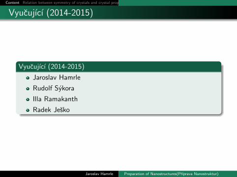
Vyucujıcı (2014-2015)
Vyucujıcı (2014-2015)
Jaroslav Hamrle
Rudolf Sykora
Illa Ramakanth
Radek Jesko
Jaroslav Hamrle Preparation of Nanostructures(Prıprava Nanostruktur)

Content Relation between symmetry of crystals and crystal properties Introduction Bulk crystal growth Thin film preparation Lateral structures ATR / Surface plasma resonance
Nabızeny obsah prednasky:
Illa Ramakanth (3 lessons)
1 Chemical deposition methods for the formation of thin films
Chemical approach (preparation)Chemical Vapor Deposition (CVD) process (chemical method)Electrodeposition and solid phase method (chemical method)Co-precipitation approach (chemical method)Sol-gel (chemical method)Hydrothermal synthesis / Solvothermal method (chemicalmethod)Ultrasonic assisted wet chemical routeSpin coating (chemical method)Lithography
2 Fullerenes: Structure, Preparation, Properties & applications
3 Carbon Nanotubes: Structure, Preparation, Properties &applications
Jaroslav Hamrle Preparation of Nanostructures(Prıprava Nanostruktur)

Content Relation between symmetry of crystals and crystal properties Introduction Bulk crystal growth Thin film preparation Lateral structures ATR / Surface plasma resonance
Nabızeny obsah prednasky:
Rudolf Sykora
krystalografie, 2D krystalografie, pocitani vzdalenosti rovin
relaxace povrchu,
elektronova struktura povrchu (kap 2 ze surface science)
kap. 8. + 9.rekonstrukce povrchu; atomova struktura povrchu
kap. 11. elektronova struktura povrchu
Radek Jesko
fyzikalnı depozice: MBE, naprasovanı (sputtering) [bude upresneno]
Jaroslav Hamrle Preparation of Nanostructures(Prıprava Nanostruktur)
Content Relation between symmetry of crystals and crystal properties Introduction Bulk crystal growth Thin film preparation Lateral structures ATR / Surface plasma resonance
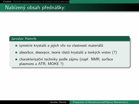
Nabızeny obsah prednasky:
Jaroslav Hamrle
symetrie krystalu a jejich vliv na vlastnosti materialu
absorbce, desorpce, teorie rustu krystalu a tenkych vrstev (?)
charakterizacnı techniky podle zajmu (napr. NMR, surfaceplasmons a ATR, MOKE ?)
Jaroslav Hamrle Preparation of Nanostructures(Prıprava Nanostruktur)
Content Relation between symmetry of crystals and crystal properties Introduction Bulk crystal growth Thin film preparation Lateral structures ATR / Surface plasma resonance
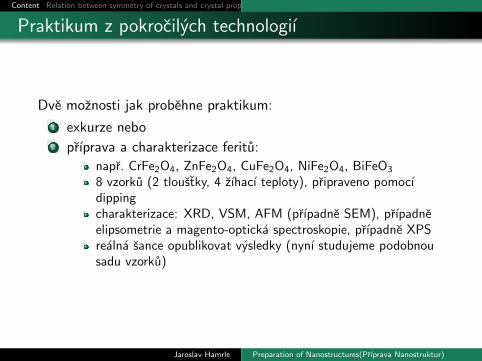
Praktikum z pokrocilych technologiı
Dve moznosti jak probehne praktikum:
1 exkurze nebo2 prıprava a charakterizace feritu:
napr. CrFe2O4, ZnFe2O4, CuFe2O4, NiFe2O4, BiFeO3
8 vzorku (2 tloustky, 4 zıhacı teploty), pripraveno pomocıdippingcharakterizace: XRD, VSM, AFM (prıpadne SEM), prıpadneelipsometrie a magento-opticka spectroskopie, prıpadne XPSrealna sance opublikovat vysledky (nynı studujeme podobnousadu vzorku)
Jaroslav Hamrle Preparation of Nanostructures(Prıprava Nanostruktur)

Content Relation between symmetry of crystals and crystal properties Introduction Bulk crystal growth Thin film preparation Lateral structures ATR / Surface plasma resonance
Outline
1 Content2 Relation between symmetry
of crystals and crystalproperties
3 Introduction
4 Bulk crystal growth5 Thin film preparation6 Lateral structures7 ATR / Surface plasma
resonance
Jaroslav Hamrle Preparation of Nanostructures(Prıprava Nanostruktur)

Content Relation between symmetry of crystals and crystal properties Introduction Bulk crystal growth Thin film preparation Lateral structures ATR / Surface plasma resonance
Type of structures
Types of structures
bulks (including bulk superstructures)
layers
2D structures (lithography, self-organizing growth)
3D structures (special lithography, 3D printing)
Jaroslav Hamrle Preparation of Nanostructures(Prıprava Nanostruktur)

Content Relation between symmetry of crystals and crystal properties Introduction Bulk crystal growth Thin film preparation Lateral structures ATR / Surface plasma resonance
Basic material structures
Basic material structures from material point of view:
single crystal (also known as monocrystals or epitaxial)
polycrystals (small single crystals randomly oriented)
amorphous (e.g. glass)
Jaroslav Hamrle Preparation of Nanostructures(Prıprava Nanostruktur)

Content Relation between symmetry of crystals and crystal properties Introduction Bulk crystal growth Thin film preparation Lateral structures ATR / Surface plasma resonance
Outline
1 Content2 Relation between symmetry
of crystals and crystalproperties
3 Introduction
4 Bulk crystal growth5 Thin film preparation6 Lateral structures7 ATR / Surface plasma
resonance
Jaroslav Hamrle Preparation of Nanostructures(Prıprava Nanostruktur)

Content Relation between symmetry of crystals and crystal properties Introduction Bulk crystal growth Thin film preparation Lateral structures ATR / Surface plasma resonance
Crystal growth techniques I: using one solvent
slow cooling of the solvent (rozpoustedlo): substances that are muchmore soluble in a solvent at high temperature than at low temperature
slow evaporation of the solvent [solvent evaporates → crystal growth]
solvent can be also liquid metal (e.g. Sn-tin)
http://en.wikipedia.org/wiki/Recrystallization_(chemistry)
Jaroslav Hamrle Preparation of Nanostructures(Prıprava Nanostruktur)

Content Relation between symmetry of crystals and crystal properties Introduction Bulk crystal growth Thin film preparation Lateral structures ATR / Surface plasma resonance
Crystal growth techniques I: using two solvents
Two solvents (substances that are very soluble in one solvent and insoluble in asecond solvent. The two solvents must be miscible, i.e. soluble in each other inall proportions):
two solvent evaporation [dissolve substance in good solvent → add badsolvent → good solvent evaporates → crystal growth in bad solvent]
two solvent liquid diffusion [dissolve substance in good solvent → addbad solvent → crystal growth in mixture of bad and good solvent].
two solvent vapour diffusion [dissolve substance in good solvent → addbad solvent to surrounding → bad solvent mixes with good throughdiffusion of vapours → crystal growth in bad solvent]
Jaroslav Hamrle Preparation of Nanostructures(Prıprava Nanostruktur)
Content Relation between symmetry of crystals and crystal properties Introduction Bulk crystal growth Thin film preparation Lateral structures ATR / Surface plasma resonance
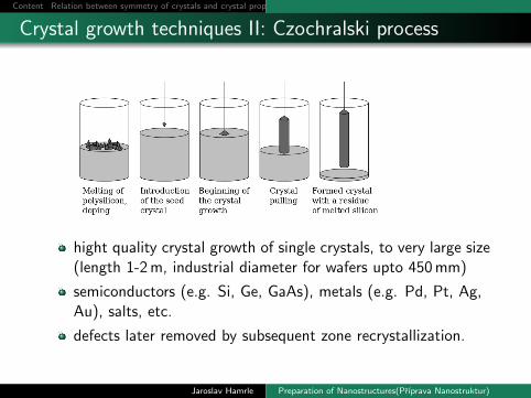
Crystal growth techniques II: Czochralski process
hight quality crystal growth of single crystals, to very large size(length 1-2 m, industrial diameter for wafers upto 450 mm)
semiconductors (e.g. Si, Ge, GaAs), metals (e.g. Pd, Pt, Ag,Au), salts, etc.
defects later removed by subsequent zone recrystallization.
Jaroslav Hamrle Preparation of Nanostructures(Prıprava Nanostruktur)

Content Relation between symmetry of crystals and crystal properties Introduction Bulk crystal growth Thin film preparation Lateral structures ATR / Surface plasma resonance
Crystal growth techniques III: Laser Heated PedestalGrowth (LHPG)
similar to Czochralski process, butno crucible needed
heating by power laser
high purity and low stress crystals
allows to growth materials withvery high melting points
when heating starts with singlecrystal on top, can produce singlecrystal
Jaroslav Hamrle Preparation of Nanostructures(Prıprava Nanostruktur)

Content Relation between symmetry of crystals and crystal properties Introduction Bulk crystal growth Thin film preparation Lateral structures ATR / Surface plasma resonance
Polycrystal growth: arc melting/remelting
melting or remelting in weekvacuum (usually Ar residualatmosphere)
creation of metalpolycrystals, with definedcomposition
allows to melt smallamounts of materials
vacuum remelting and slowcooling: removal of residualgas and high vapour pressureelements (C,S,O,Mg), largercrystal size, stable structureobtained.
Huag et al, Materials Science and Engineering: A 422, 309, (2006)
Jaroslav Hamrle Preparation of Nanostructures(Prıprava Nanostruktur)

Content Relation between symmetry of crystals and crystal properties Introduction Bulk crystal growth Thin film preparation Lateral structures ATR / Surface plasma resonance
Crystal growth: nucleation
1. Crystal nucleation:
small particle of crystal is created (nucleated), with randomcrystallographic orientation.
homogenous/heterogenous (without/with influence of theexternal particle).
nucleus appears slowly (then crystal may growth quickly).
external crystal can be used as a seed.
Jaroslav Hamrle Preparation of Nanostructures(Prıprava Nanostruktur)

Content Relation between symmetry of crystals and crystal properties Introduction Bulk crystal growth Thin film preparation Lateral structures ATR / Surface plasma resonance
Crystal growth: growth
2. Crystal growth:
In ideal case, crystal grows layer by layer added to thenucleated seed. The interface between crystal andvapour/solvent is atomically sharp.
Non-uniform lateral growth: The surface advances by thelateral motion of steps which are one interplanar spacing inheight.
Uniform lateral growth: The surface advances normal to itselfwithout the necessity of a stepwise growth mechanism.
Jaroslav Hamrle Preparation of Nanostructures(Prıprava Nanostruktur)

Content Relation between symmetry of crystals and crystal properties Introduction Bulk crystal growth Thin film preparation Lateral structures ATR / Surface plasma resonance
Outline
1 Content2 Relation between symmetry
of crystals and crystalproperties
3 Introduction
4 Bulk crystal growth5 Thin film preparation6 Lateral structures7 ATR / Surface plasma
resonance
Jaroslav Hamrle Preparation of Nanostructures(Prıprava Nanostruktur)

Content Relation between symmetry of crystals and crystal properties Introduction Bulk crystal growth Thin film preparation Lateral structures ATR / Surface plasma resonance
Thin film preparation
Techniques of thin film preparation
physical techniques (usually physical vapour deposition,differing by source of vapour (MBE, sputtering, ion plating))
chemical techniques (spin coating, chemical solutiondeposition (sol-gel), chemical vapour deposition)
Jaroslav Hamrle Preparation of Nanostructures(Prıprava Nanostruktur)

Content Relation between symmetry of crystals and crystal properties Introduction Bulk crystal growth Thin film preparation Lateral structures ATR / Surface plasma resonance
Physical depostion techniques: physical vapour deposition(PVD)
PVD involes: Vapour formation → vapourtransformation → film formation
Vapour phase creation:evaporation
sputtering
ion plating
Vapour transportation:
collisions (can be related with clusterformation)
ionizations
Condensation on substrate:nucleation, growth, ion bombardment,redeposition etc.
Jaroslav Hamrle Preparation of Nanostructures(Prıprava Nanostruktur)
Content Relation between symmetry of crystals and crystal properties Introduction Bulk crystal growth Thin film preparation Lateral structures ATR / Surface plasma resonance
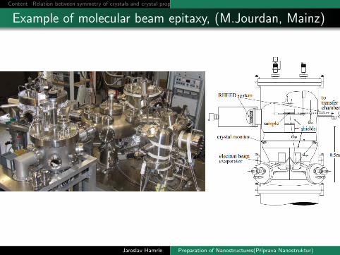
Example of molecular beam epitaxy, (M.Jourdan, Mainz)
Jaroslav Hamrle Preparation of Nanostructures(Prıprava Nanostruktur)

Content Relation between symmetry of crystals and crystal properties Introduction Bulk crystal growth Thin film preparation Lateral structures ATR / Surface plasma resonance
Sources of vapours I: electron beam evaporators
Local heating by electronbombardment → evaporation of thetarget material → clean depositionof the target
www.mbe-components.com
Jaroslav Hamrle Preparation of Nanostructures(Prıprava Nanostruktur)

Content Relation between symmetry of crystals and crystal properties Introduction Bulk crystal growth Thin film preparation Lateral structures ATR / Surface plasma resonance
Source of vapours II: Effusion cells (Knudsen Cell)
Thermal evaporation out of a heatedcrucible (Tmax ≈ 1800◦C)
www.mbe-components.com
Jaroslav Hamrle Preparation of Nanostructures(Prıprava Nanostruktur)
Content Relation between symmetry of crystals and crystal properties Introduction Bulk crystal growth Thin film preparation Lateral structures ATR / Surface plasma resonance
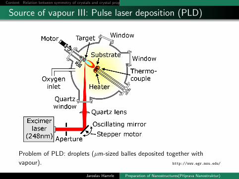
Source of vapour III: Pulse laser deposition (PLD)
Problem of PLD: droplets (µm-sized balles deposited together with
vapour). http://www.egr.msu.edu/
Jaroslav Hamrle Preparation of Nanostructures(Prıprava Nanostruktur)
Content Relation between symmetry of crystals and crystal properties Introduction Bulk crystal growth Thin film preparation Lateral structures ATR / Surface plasma resonance
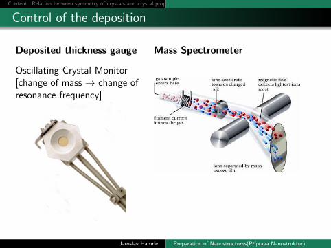
Control of the deposition
Deposited thickness gauge
Oscillating Crystal Monitor[change of mass → change ofresonance frequency]
Mass Spectrometer
Jaroslav Hamrle Preparation of Nanostructures(Prıprava Nanostruktur)

Content Relation between symmetry of crystals and crystal properties Introduction Bulk crystal growth Thin film preparation Lateral structures ATR / Surface plasma resonance
Sputtering
Sputtering:
ejection of atoms from target due to bombardment ofenergetic particles (E � 1 eV ).
commonly use for thin-film deposition, etching or analyticalmaterial study.
1 create plasma (dc, rf, mw)2 plasma looses energy to surroundings (bombardment)3 for plasma, atoms of noble gas of similar weight as target is
used (e.g. Ar for 3d metals)
Jaroslav Hamrle Preparation of Nanostructures(Prıprava Nanostruktur)

Content Relation between symmetry of crystals and crystal properties Introduction Bulk crystal growth Thin film preparation Lateral structures ATR / Surface plasma resonance
dc-sputtering
http://www.ajaint.com/whatis.htm
Jaroslav Hamrle Preparation of Nanostructures(Prıprava Nanostruktur)

Content Relation between symmetry of crystals and crystal properties Introduction Bulk crystal growth Thin film preparation Lateral structures ATR / Surface plasma resonance
dc-sputtering: Glow Discharge
Jaroslav Hamrle Preparation of Nanostructures(Prıprava Nanostruktur)

Content Relation between symmetry of crystals and crystal properties Introduction Bulk crystal growth Thin film preparation Lateral structures ATR / Surface plasma resonance
Sputtering: example
Jaroslav Hamrle Preparation of Nanostructures(Prıprava Nanostruktur)

Content Relation between symmetry of crystals and crystal properties Introduction Bulk crystal growth Thin film preparation Lateral structures ATR / Surface plasma resonance
Sputtering: industrial sputtering of glass
Jaroslav Hamrle Preparation of Nanostructures(Prıprava Nanostruktur)

Content Relation between symmetry of crystals and crystal properties Introduction Bulk crystal growth Thin film preparation Lateral structures ATR / Surface plasma resonance
Sputtering: magnetron
Jaroslav Hamrle Preparation of Nanostructures(Prıprava Nanostruktur)

Content Relation between symmetry of crystals and crystal properties Introduction Bulk crystal growth Thin film preparation Lateral structures ATR / Surface plasma resonance
Sputtering: magnetron
Added magnetic field drives free electrons:
electrons do not touch the target, and hence do not heat it
electrons are localized above the target, and hence enhancingprobability of ionization of nobel gas ⇒ increases depositionrates
reccombination of free electrons and ions ⇒ glowing plasma
Jaroslav Hamrle Preparation of Nanostructures(Prıprava Nanostruktur)

Content Relation between symmetry of crystals and crystal properties Introduction Bulk crystal growth Thin film preparation Lateral structures ATR / Surface plasma resonance
Sputtering: magnetron
Jaroslav Hamrle Preparation of Nanostructures(Prıprava Nanostruktur)

Content Relation between symmetry of crystals and crystal properties Introduction Bulk crystal growth Thin film preparation Lateral structures ATR / Surface plasma resonance
Sputtering: rf sputtering
• Plasma is generated by radio-frequency (rf) field (MHz).
• Rf-sputtering avoids charge build-up on insulating targets (e.g. allows
to sputter oxides).
Jaroslav Hamrle Preparation of Nanostructures(Prıprava Nanostruktur)

Content Relation between symmetry of crystals and crystal properties Introduction Bulk crystal growth Thin film preparation Lateral structures ATR / Surface plasma resonance
Ion plating
Atoms of target are ionized, to increase their speed prior thedeposition → atom can penetrate deeper into the substrateGoal (1): placement of atoms into substrate:
gold plating
steel hardening (e.g. layer of TiN)
Goal (2): crystal defects caused by atom irradiation:
interface roughness control (magnetization anisotropy control)
defects in AFM/FM interface ⇒ exchange bias control
. . .
Jaroslav Hamrle Preparation of Nanostructures(Prıprava Nanostruktur)

Content Relation between symmetry of crystals and crystal properties Introduction Bulk crystal growth Thin film preparation Lateral structures ATR / Surface plasma resonance
PVD techniques - comparison
http://www.eclatcoating.com/learn/pvdcoating.php
Jaroslav Hamrle Preparation of Nanostructures(Prıprava Nanostruktur)
Content Relation between symmetry of crystals and crystal properties Introduction Bulk crystal growth Thin film preparation Lateral structures ATR / Surface plasma resonance
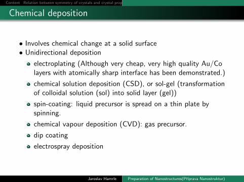
Chemical deposition
• Involves chemical change at a solid surface• Unidirectional deposition
electroplating (Although very cheap, very high quality Au/Colayers with atomically sharp interface has been demonstrated.)
chemical solution deposition (CSD), or sol-gel (transformationof colloidal solution (sol) into solid layer (gel))
spin-coating: liquid precursor is spread on a thin plate byspinning.
chemical vapour deposition (CVD): gas precursor.
dip coating
electrospray deposition
Jaroslav Hamrle Preparation of Nanostructures(Prıprava Nanostruktur)

Content Relation between symmetry of crystals and crystal properties Introduction Bulk crystal growth Thin film preparation Lateral structures ATR / Surface plasma resonance
Chemical vapour deposition (CVD)
Film components boundin gas molecules
Gas molecules directedon heated substrate
Chemical reactioncreates film material
Gaseous by-products
GaN deposition(NH3+TriMetylGalium)
http://thermodynamik.uni-duisburg.de/mitarbeiter/atakan/cvd_intro.htm
Jaroslav Hamrle Preparation of Nanostructures(Prıprava Nanostruktur)
Content Relation between symmetry of crystals and crystal properties Introduction Bulk crystal growth Thin film preparation Lateral structures ATR / Surface plasma resonance
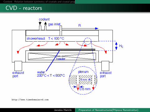
CVD - reactors
http://www.timedomaincvd.com
Jaroslav Hamrle Preparation of Nanostructures(Prıprava Nanostruktur)

Content Relation between symmetry of crystals and crystal properties Introduction Bulk crystal growth Thin film preparation Lateral structures ATR / Surface plasma resonance
Jaroslav Hamrle Preparation of Nanostructures(Prıprava Nanostruktur)

Content Relation between symmetry of crystals and crystal properties Introduction Bulk crystal growth Thin film preparation Lateral structures ATR / Surface plasma resonance
Jaroslav Hamrle Preparation of Nanostructures(Prıprava Nanostruktur)

Content Relation between symmetry of crystals and crystal properties Introduction Bulk crystal growth Thin film preparation Lateral structures ATR / Surface plasma resonance
Jaroslav Hamrle Preparation of Nanostructures(Prıprava Nanostruktur)

Content Relation between symmetry of crystals and crystal properties Introduction Bulk crystal growth Thin film preparation Lateral structures ATR / Surface plasma resonance
Ele
ctro
spra
yd
epo
siti
on
http://rsl.eng.usf.edu/Pages/ResearchElectrosprayAmbient.html
Jaroslav Hamrle Preparation of Nanostructures(Prıprava Nanostruktur)

Content Relation between symmetry of crystals and crystal properties Introduction Bulk crystal growth Thin film preparation Lateral structures ATR / Surface plasma resonance
Outline
1 Content2 Relation between symmetry
of crystals and crystalproperties
3 Introduction
4 Bulk crystal growth5 Thin film preparation6 Lateral structures7 ATR / Surface plasma
resonance
Jaroslav Hamrle Preparation of Nanostructures(Prıprava Nanostruktur)
Content Relation between symmetry of crystals and crystal properties Introduction Bulk crystal growth Thin film preparation Lateral structures ATR / Surface plasma resonance
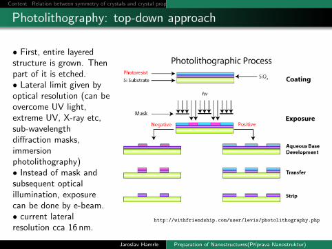
Photolithography: top-down approach
• First, entire layeredstructure is grown. Thenpart of it is etched.• Lateral limit given byoptical resolution (can beovercome UV light,extreme UV, X-ray etc,sub-wavelengthdiffraction masks,immersionphotolithography)• Instead of mask andsubsequent opticalillumination, exposurecan be done by e-beam.• current lateralresolution cca 16 nm.
http://withfriendship.com/user/levis/photolithography.php
Jaroslav Hamrle Preparation of Nanostructures(Prıprava Nanostruktur)

Content Relation between symmetry of crystals and crystal properties Introduction Bulk crystal growth Thin film preparation Lateral structures ATR / Surface plasma resonance
Lithography: standard and lift-off process
Lift-off: mainly to have goodmetal/metal interface.Advantages:•do not need etching.Disadvantages•Retention: not all (usuallymetallic) layer is washed outand stays on the wafer.•Ears: When the metal isdeposited, and it covers thesidewalls of the resist, ”ears”can be formed.•Redeposition: it is possiblethat particles of metal willbecome reattached to thesurface, at a randomlocation.
http://www.microresist.de
Jaroslav Hamrle Preparation of Nanostructures(Prıprava Nanostruktur)

Content Relation between symmetry of crystals and crystal properties Introduction Bulk crystal growth Thin film preparation Lateral structures ATR / Surface plasma resonance
Focused ion beam (FIB) nanofabrication
Focused ion beam (FIB):
1 source of ions (usually Ga+ orHe+)
2 beam optics (similar to scanningelectron microscopy)
3 ions ar focused to sample surface(focus diameter down to 1 nm)
4 local remove of atoms by ions(FIB-milling) http://web2.ges.gla.ac.uk/~mlee/FIBtec.htm
Jaroslav Hamrle Preparation of Nanostructures(Prıprava Nanostruktur)

Content Relation between symmetry of crystals and crystal properties Introduction Bulk crystal growth Thin film preparation Lateral structures ATR / Surface plasma resonance
FIB nanostructures examples
http://nano.aalto.fi/en/research/groups/mqs/
research/micro_and_nanofabrication/
www.raith.com
Jaroslav Hamrle Preparation of Nanostructures(Prıprava Nanostruktur)

Content Relation between symmetry of crystals and crystal properties Introduction Bulk crystal growth Thin film preparation Lateral structures ATR / Surface plasma resonance
Bottom-up approach
The opposite of thetop-down approach.
Instead of taking materialaway to make structures, thebottom-up approachselectively adds atoms tocreate structures.
http://idol.union.edu/~malekis/ESC24/KoskywebModules/sa_topd.htm
Jaroslav Hamrle Preparation of Nanostructures(Prıprava Nanostruktur)

Content Relation between symmetry of crystals and crystal properties Introduction Bulk crystal growth Thin film preparation Lateral structures ATR / Surface plasma resonance
The Ideas Behind the Bottom-up Approach
Nature uses the bottom upapproach.
Cells
Crystals
Humans
Chemistry and biology can helpto assemble and control growth. http://www.csacs.mcgill.ca/selfassembly.htm
Jaroslav Hamrle Preparation of Nanostructures(Prıprava Nanostruktur)

Content Relation between symmetry of crystals and crystal properties Introduction Bulk crystal growth Thin film preparation Lateral structures ATR / Surface plasma resonance
Why is Bottom-Up Processing Needed?
Allows smaller geometries than photolithography.
Certain structures such as Carbon Nanotubes and Sinanowires are grown through a bottom-up process.
New technologies such as organic semiconductors employbottom-up processes to pattern them.
Can make formation of films and structures much easier.
Is more economical than top-down in that it does not wastematerial to etching.
http://courses.ee.psu.edu/ruzyllo/ee518/EE518_Top-down%20and%20Bottom-up1.ppt
Jaroslav Hamrle Preparation of Nanostructures(Prıprava Nanostruktur)

Content Relation between symmetry of crystals and crystal properties Introduction Bulk crystal growth Thin film preparation Lateral structures ATR / Surface plasma resonance
Self Assembly
The principle behind bottom-up processing.
Self assembly is the coordinated action of independent entitiesto produce larger, ordered structures or achieve a desiredshape.
Found in nature.
Start on the atomic scale.
Jaroslav Hamrle Preparation of Nanostructures(Prıprava Nanostruktur)

Content Relation between symmetry of crystals and crystal properties Introduction Bulk crystal growth Thin film preparation Lateral structures ATR / Surface plasma resonance
Example 1: self-assembled nanodots
1) Self-assembled monolayer of 340 nm-diameter polystyrene spheres2) Ni film deposited and balls removed
AppliedSurfaceScience257,8712,(2011)
Jaroslav Hamrle Preparation of Nanostructures(Prıprava Nanostruktur)

Content Relation between symmetry of crystals and crystal properties Introduction Bulk crystal growth Thin film preparation Lateral structures ATR / Surface plasma resonance
Example 2: Self-assembled Monolayers (SAMS)
Molecules are depositedmolecule-by-molecule to form aself-assembled monolayer.
Creates a high quality layers.
Layers are deposited one layer at atime.
Organic molecules can’t be depositedusing extreme conditions because itwould damage the organic molecules.
SAMS technique does not damageorganic molecules.
SAMS films are nearly defect free.
Used to deposit organicsemiconductors.
http://www.mtl.kyoto-u.ac.jp/english/
laboratory/nanoscopic/nanoscopic.htm
http://www.seas.upenn.edu/
Jaroslav Hamrle Preparation of Nanostructures(Prıprava Nanostruktur)

Content Relation between symmetry of crystals and crystal properties Introduction Bulk crystal growth Thin film preparation Lateral structures ATR / Surface plasma resonance
Other examples of self assembly
carbon nanotubes
. . .
Jaroslav Hamrle Preparation of Nanostructures(Prıprava Nanostruktur)

Content Relation between symmetry of crystals and crystal properties Introduction Bulk crystal growth Thin film preparation Lateral structures ATR / Surface plasma resonance
Outline
1 Content2 Relation between symmetry
of crystals and crystalproperties
3 Introduction
4 Bulk crystal growth5 Thin film preparation6 Lateral structures7 ATR / Surface plasma
resonance
Jaroslav Hamrle Preparation of Nanostructures(Prıprava Nanostruktur)

Content Relation between symmetry of crystals and crystal properties Introduction Bulk crystal growth Thin film preparation Lateral structures ATR / Surface plasma resonance
Reflection and total reflection
Snell law:
√ε1 sinϕ1 =
√ε2 sinϕ2
Critical angle:
sinϕc =
√ε2
ε1
Jaroslav Hamrle Preparation of Nanostructures(Prıprava Nanostruktur)

Content Relation between symmetry of crystals and crystal properties Introduction Bulk crystal growth Thin film preparation Lateral structures ATR / Surface plasma resonance
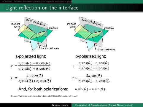
Light reflection on the interface
1 Maxwell equations
2 solution as plane waveE = E0 exp(i(~k ·~r − ωt))
3 boundary conditions at theinterface:~E , ~H fields: continuoustransverse (x , y) components~D, ~B fields: continuous normal(z) components
4 for total reflection, solution oftransverse wave is in form socalled evanescent wave,non-propagating in z-directionE = E exp(−kzz)
Jaroslav Hamrle Preparation of Nanostructures(Prıprava Nanostruktur)
Content Relation between symmetry of crystals and crystal properties Introduction Bulk crystal growth Thin film preparation Lateral structures ATR / Surface plasma resonance
Light reflection on the interface
http://www.ece.rice.edu/~daniel/262/pdf/lecture14.pdf
Jaroslav Hamrle Preparation of Nanostructures(Prıprava Nanostruktur)

Content Relation between symmetry of crystals and crystal properties Introduction Bulk crystal growth Thin film preparation Lateral structures ATR / Surface plasma resonance
Light reflection on the interface
Reflection on glass/air
Jaroslav Hamrle Preparation of Nanostructures(Prıprava Nanostruktur)

Content Relation between symmetry of crystals and crystal properties Introduction Bulk crystal growth Thin film preparation Lateral structures ATR / Surface plasma resonance
Total reflection
Critical angle:
sinϕc =
√ε2
ε1=
n2
n1
Evanescent wave:
E = Et exp(−z/δ − iωt)
Penetration depth:
δ =1
k0
√(n1 sinϕ1)2 − (n2
2)
Example: glass(n1)/water(n2)inteerface; n1 > n2
http://www.tirftechnologies.com/principles.php
Jaroslav Hamrle Preparation of Nanostructures(Prıprava Nanostruktur)

Content Relation between symmetry of crystals and crystal properties Introduction Bulk crystal growth Thin film preparation Lateral structures ATR / Surface plasma resonance
Attenuated total reflectance (ATR)
(Zeslabeny uplny odraz)
probes sample by evanescentwave
⇒ sensitive to surface of thesample
sample modifies evanescentwave → partial absorption ortransmission of light in sample→ total reflection is decreased(attenuated).
reflected beam does not followexactly geometrical optics →The Goos-Hanchen shift
Jaroslav Hamrle Preparation of Nanostructures(Prıprava Nanostruktur)

Content Relation between symmetry of crystals and crystal properties Introduction Bulk crystal growth Thin film preparation Lateral structures ATR / Surface plasma resonance
Attenuated total reflectance (ATR): gap effect
Gap thickness (refractivity ofgap=1):
Absorption in gap (gap thickness960 nm):
Jaroslav Hamrle Preparation of Nanostructures(Prıprava Nanostruktur)

Content Relation between symmetry of crystals and crystal properties Introduction Bulk crystal growth Thin film preparation Lateral structures ATR / Surface plasma resonance
Surface plasmon I: derivation
Electric field in the vicinity of the interface:
E = EO exp[i(kxx + kzz − ωt)]
where
k2 = k2x + k2
z = ε (ω/c)2 = εk20 (1)
At the interface of two materials ε1 and ε2:(a) kx continuous over the interface;
kx1 = kx2 (2)
(b) Dz and Ex continuous over the interface
kz1/ε1 = kz2/ε2 (3) http://www.physics.uwo.ca/~smittler/
Jaroslav Hamrle Preparation of Nanostructures(Prıprava Nanostruktur)

Content Relation between symmetry of crystals and crystal properties Introduction Bulk crystal growth Thin film preparation Lateral structures ATR / Surface plasma resonance
Surface plasmon II: dispersion relation
• From Eqs.(1–3) followsdispersion relation for surfaceplasmon:
kx = k0
√(ε1ε2
ε1 + ε2
), (4)
where k0 = ω/c .• Surface plasmon appears onlyfor p-polarized (TM) wave, asthis mode has normal (z)component of D = εε0E field.
Jaroslav Hamrle Preparation of Nanostructures(Prıprava Nanostruktur)
Content Relation between symmetry of crystals and crystal properties Introduction Bulk crystal growth Thin film preparation Lateral structures ATR / Surface plasma resonance
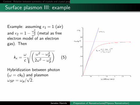
Surface plasmon III: example
Example: assuming ε1 = 1 (air)
and ε2 = 1− ω2p
ω2 (metal as freeelectron model of an electrongas). Then
kx =ω
c
√(ω2 − ω2
p
2ω2 − ω2p
)(5)
Hybridization between photon(ω = ck0) and plasmonωSP = ωp/
√2.
Jaroslav Hamrle Preparation of Nanostructures(Prıprava Nanostruktur)
Content Relation between symmetry of crystals and crystal properties Introduction Bulk crystal growth Thin film preparation Lateral structures ATR / Surface plasma resonance
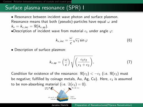
Surface plasma resonance (SPR) I
• Resonance between incident wave photon and surface plasmon.Resonance means that both (pseudo)-particles have equal ω andkx = kx,inc = <(kx,sp).•Description of incident wave from material ε1 under angle ϕ:
kx,inc =ω
c
√ε1 sinϕ (6)
• Description of surface plasmon:
kx,sp =(ω
c
)√( ε1ε2
ε1 + ε2
), (7)
Condition for existence of the resonance: <(ε2) < −ε1 (i.e. <(ε2) must
be negative; fulfilled by coinage metals, Au, Ag, Cu). Here, ε1 is assumed
to be non-absorbing material (i.e. =(ε1) = 0).
Jaroslav Hamrle Preparation of Nanostructures(Prıprava Nanostruktur)
Content Relation between symmetry of crystals and crystal properties Introduction Bulk crystal growth Thin film preparation Lateral structures ATR / Surface plasma resonance
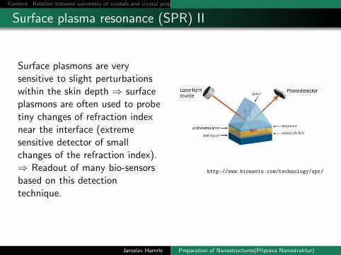
Surface plasma resonance (SPR) II
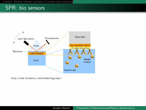
Surface plasmons are verysensitive to slight perturbationswithin the skin depth ⇒ surfaceplasmons are often used to probetiny changes of refraction indexnear the interface (extremesensitive detector of smallchanges of the refraction index).⇒ Readout of many bio-sensorsbased on this detectiontechnique.
http://www.bionavis.com/technology/spr/
Jaroslav Hamrle Preparation of Nanostructures(Prıprava Nanostruktur)

Content Relation between symmetry of crystals and crystal properties Introduction Bulk crystal growth Thin film preparation Lateral structures ATR / Surface plasma resonance
SPR: detection I
• presence of resonanceincreases absorptionand reduces reflectivity.• position of reflectionminima very sensitiveto refractivity index inposition of theevanescent wave.
Jaroslav Hamrle Preparation of Nanostructures(Prıprava Nanostruktur)

Content Relation between symmetry of crystals and crystal properties Introduction Bulk crystal growth Thin film preparation Lateral structures ATR / Surface plasma resonance
SPR: detection II
• presence of resonanceincreases absorptionand reduces reflectivity.• position of reflectionminima very sensitiveto refractivity index inposition of theevanescent wave.
Jaroslav Hamrle Preparation of Nanostructures(Prıprava Nanostruktur)
Content Relation between symmetry of crystals and crystal properties Introduction Bulk crystal growth Thin film preparation Lateral structures ATR / Surface plasma resonance
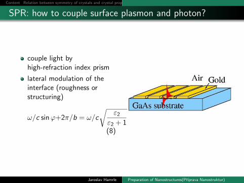
SPR: how to couple surface plasmon and photon?
couple light byhigh-refraction index prism
lateral modulation of theinterface (roughness orstructuring)
ω/c sinϕ+2π/b = ω/c
√ε2
ε2 + 1(8)
Jaroslav Hamrle Preparation of Nanostructures(Prıprava Nanostruktur)
Content Relation between symmetry of crystals and crystal properties Introduction Bulk crystal growth Thin film preparation Lateral structures ATR / Surface plasma resonance
SPR: bio sensors
http://www.bionavis.com/technology/spr/
Jaroslav Hamrle Preparation of Nanostructures(Prıprava Nanostruktur)