Embed Size (px)
Citation preview
lable at ScienceDirect
Current Applied Physics 11 (2011) 657e661
Contents lists avai
Current Applied Physics
journal homepage: www.elsevier .com/locate/cap
Preparing large-scale WO3 nanowire-like structure for high sensitivity NH3 gassensor through a simple route
Nguyen Van Hieu a,*, Vu Van Quang a, Nguyen Duc Hoa a,**, Dojin Kim b,***
a International Training Institute for Materials Science (ITIMS), Hanoi University of Science and Technology (HUST), Hanoi, VietnambDepartment of Materials Science and Engineering, Chungnam National University, Daejeon, Republic of Korea
a r t i c l e i n f o
Article history:Received 29 July 2010Received in revised form13 October 2010Accepted 1 November 2010Available online 27 November 2010
Keywords:WO3 nanowiresSWCNTs templateNH3 sensors
* Corresponding author. No. 1, Dai Co Viet Road,38680787; fax: þ84 4 38692963.** Corresponding author.*** Corresponding author.
E-mail addresses: [email protected] (N.V.(N.D. Hoa), [email protected] (D. Kim).
1567-1739/$ e see front matter � 2010 Elsevier B.V.doi:10.1016/j.cap.2010.11.002
a b s t r a c t
The large-scale nanowire-like (NW) structure of tungsten oxide is synthesized by the deposition oftungsten metal on the substrate of porous single-wall carbon nanotubes (SWCNTs) film, followed bythermal oxidation process. The morphology and crystallinity of the synthesized materials are analyzed bySEM, TEM, XRD, and Raman spectroscopy. Results showed that tungsten oxide NWs deposited on SWCNTshave a porous structure with an average diameter of about 70 nm and a length of up to micrometers. TheNH3 gas-sensing properties of tungsten NWs were measured at different temperatures. A maximumresponse of 9.7e1500 ppm at 250 �C with rapid response and recovery times of 7 and 8 s are found,respectively. In addition, the gas sensing mechanism of fabricated NWs is also discussed in term of surfaceresistivity and barrier height model.
� 2010 Elsevier B.V. All rights reserved.
1. Introduction
Nanostructured tungsten oxide materials have receivedtremendous interest in recent years because of their great potentialapplications as gas sensors [1,2], field emission devices [3], andphotocatalysts [4]. Nanostructured tungsten oxide based gassensors have been used for detecting a variety of gases, such as NO2,CO, H2, SO2, H2, and NH3 [1,2,5,6]. In particular, nanostructuredtungsten oxides like nanorods [7] and nanowires [8] can be used ashigh sensitive gas sensors, which are unattainable by the conven-tional materials. Nanostructured tungsten oxide nanorods, nano-wires, nanotubes, nanoflakes and nanodisks have been synthesizedbyusinghigh temperature evaporation, precipitation, hydrothermalreaction, and electrochemical or template assisted methods [2].However, those mentioned methods have some drawbacks in gassensing devices fabrication, especially for mass production becausethey requiremultiples synthesis processes including of (i) growth ofnanowires, (ii) collection of nanowires, (iii) dispersal of the nano-wires on solution, and (iv) deposition or alignment of nanowires onpatterned metal electrodes [9,10]. These techniques require the useof expensive equipments such as an electron-beam lithography,focus ion beam and sputtering system to fabricate the electrical
Hanoi, Vietnam. Tel.: þ84 4
Hieu), [email protected]
All rights reserved.
contacts. These approaches also present a series of uncontrollableprocesses such as sonification and dispersal of nanowires on pre-fabricated electrodes. Recently, we developed a new method forsynthesizing tin oxide nanowires for gas sensor applications usingSWCNTs as templates [11]. Themethod features: (i) the versatility ofmetal choice for the nanowires structure; (ii) easy control of thediameters, andmost importantly; (iii) high porosity in the ensemblestructure.
In this study, we report on the synthesis and characterization ofNH3 gas sensing of tungsten oxide nanowires-like structure (NWs)synthesized using SWCNTas templates. These preparation processesare expected to have importance for the mass-production of othermetal oxides NWs gas sensors and quick implementation of the gassensing applications of metal oxides nanowires.
2. Experimental
The fabrication of WO3 NWs structures was carried out by (i)growing porous SWNTs as templates; (ii) depositing tungsten; and(iii) oxidizing tungsten. Briefly, SWNTs were synthesized directlyon a SiO2/Si substrate located on the insidewall of the arc-dischargechamber [11]. The deposition of tungsten on this SWCNT substratewas carried out with a DC sputtering system, in which a 2-inchtungsten target (purity of 4N) was used. The deposition was per-formed at room temperature and an Ar working pressure of2 � 10�3 Torr. The deposition power was controlled at 13 W andmaintained for 3 min to achieve a film thickness of 100 nm on theplane. During the deposition, the substrate was rotated for uniform
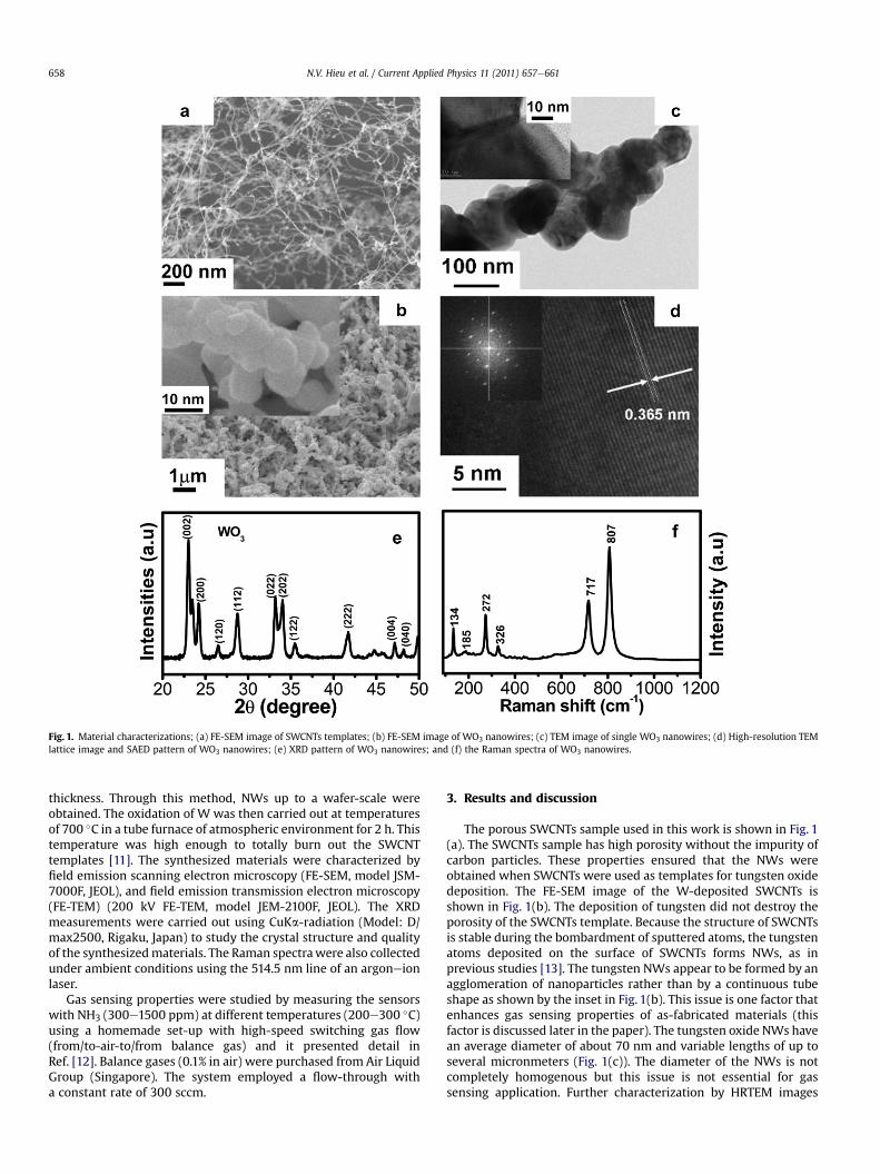
Fig. 1. Material characterizations; (a) FE-SEM image of SWCNTs templates; (b) FE-SEM image of WO3 nanowires; (c) TEM image of single WO3 nanowires; (d) High-resolution TEMlattice image and SAED pattern of WO3 nanowires; (e) XRD pattern of WO3 nanowires; and (f) the Raman spectra of WO3 nanowires.
N.V. Hieu et al. / Current Applied Physics 11 (2011) 657e661658
thickness. Through this method, NWs up to a wafer-scale wereobtained. The oxidation of W was then carried out at temperaturesof 700 �C in a tube furnace of atmospheric environment for 2 h. Thistemperature was high enough to totally burn out the SWCNTtemplates [11]. The synthesized materials were characterized byfield emission scanning electron microscopy (FE-SEM, model JSM-7000F, JEOL), and field emission transmission electron microscopy(FE-TEM) (200 kV FE-TEM, model JEM-2100F, JEOL). The XRDmeasurements were carried out using CuKa-radiation (Model: D/max2500, Rigaku, Japan) to study the crystal structure and qualityof the synthesizedmaterials. The Raman spectrawere also collectedunder ambient conditions using the 514.5 nm line of an argoneionlaser.
Gas sensing properties were studied by measuring the sensorswith NH3 (300e1500 ppm) at different temperatures (200e300 �C)using a homemade set-up with high-speed switching gas flow(from/to-air-to/from balance gas) and it presented detail inRef. [12]. Balance gases (0.1% in air) were purchased from Air LiquidGroup (Singapore). The system employed a flow-through witha constant rate of 300 sccm.
3. Results and discussion
The porous SWCNTs sample used in this work is shown in Fig. 1(a). The SWCNTs sample has high porosity without the impurity ofcarbon particles. These properties ensured that the NWs wereobtained when SWCNTs were used as templates for tungsten oxidedeposition. The FE-SEM image of the W-deposited SWCNTs isshown in Fig. 1(b). The deposition of tungsten did not destroy theporosity of the SWCNTs template. Because the structure of SWCNTsis stable during the bombardment of sputtered atoms, the tungstenatoms deposited on the surface of SWCNTs forms NWs, as inprevious studies [13]. The tungsten NWs appear to be formed by anagglomeration of nanoparticles rather than by a continuous tubeshape as shown by the inset in Fig. 1(b). This issue is one factor thatenhances gas sensing properties of as-fabricated materials (thisfactor is discussed later in the paper). The tungsten oxide NWs havean average diameter of about 70 nm and variable lengths of up toseveral micronmeters (Fig. 1(c)). The diameter of the NWs is notcompletely homogenous but this issue is not essential for gassensing application. Further characterization by HRTEM images
N.V. Hieu et al. / Current Applied Physics 11 (2011) 657e661 659
also confirms that the NWs are formed by the agglomeration ofnanoparticles rather than by a continuous tube shape. The inset inFig. 1(c) showed the grain boundary between two nanoparticleshaving different crystalline orientations. Each nanoparticle isa single crystal as revealed by the magnified HRTEM image (Fig. 1(d)), which shows clear lattice fringes with a distance of 0.36 nmbelonging to the (200) plane of monoclinic WO3. The single crystalof nanoparticles was also confirmed by the selective area electrondiffraction (SAED) pattern illustrated in the inset of Fig. 1(d). Thebright dots in the pattern indicate single crystallinity of WO3.
Fig. 1(e) shows the XRD patterns of the synthesized WO3 NWsafter oxidation process. The peaks of XRD patterns can satisfactorilymatch with the documented diffraction pattern of monoclinic WO3(JCPDS card no. 43-1035). There is no diffraction peak of metallictungsten indicating a complete oxidation at 700 �C.
Fig. 1(f) shows a typical Raman spectrum ofWO3 NWswhere sixwell-resolved peaks can be observed (134, 185, 272, 326, 717 and807 cm�1). The comparison of Raman spectra recorded on the WO3NWs with those reported in the literature [14,15] suggested thatthey have the monoclinic phase and are formed by OeWeOmicrocrystalline clusters connected to each other by WeOeW
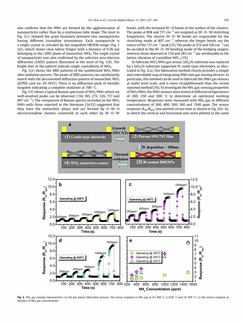
Fig. 2. NH3 gas sensing characteristics (a) the gas sensor fabrication process; the sensor refunction of NH3 gas concentration.
bonds, with the terminal WeO bonds at the surface of the clusters.The peaks at 808 and 717 cm�1 are assigned as WeOeW stretchingfrequencies. The shorter WeOeW bonds are responsible for thestretching mode at 807 cm�1, whereas the longer bonds are thesource of the 717 cm�1 peak [15]. The peaks at 272 and 326 cm�1 canbe ascribed to the WeOeW bending mode of the bridging oxygen,whereas those observed at 134 and 185 cm�1 are attributable to thelattice vibration of crystalline WO 3 [15].
To fabricateWO3 NWs gas sensor, SiO2/Si substratewas replacedby a SiO2/Si substrate supported Pt comb-type electrodes, as illus-trated in Fig. 2(a). Our fabrication method clearly provides a simpleand controllableway of integrating NWs into gas sensing devices. Inparticular, thismethod can be used to fabricate the NWs gas sensorsat wafer level scale, and is more straightforward than the recentreportedmethod [16]. To investigate theNH3 gas-sensing propertiesofWO3NWs, theNWs sensorswere tested at different temperaturesof 200, 250 and 300 �C to determine an optimized workingtemperature. Responses were measured with NH3 gas at differentconcentrations of 300, 400, 500, 100 and 1500 ppm. The sensorresponse (Rair/Rgas) was plotted versus time as shown in Fig. 2(bed),in which the vertical and horizontal axes were plotted in the same
sponse to NH3 gas at (b) 200 �C, (c)250 �C and (d) 300 �C; (e) the sensor response as
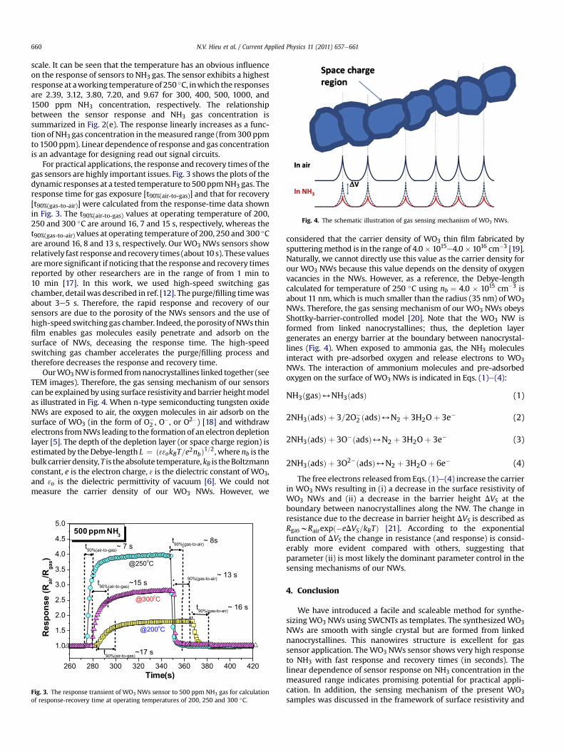
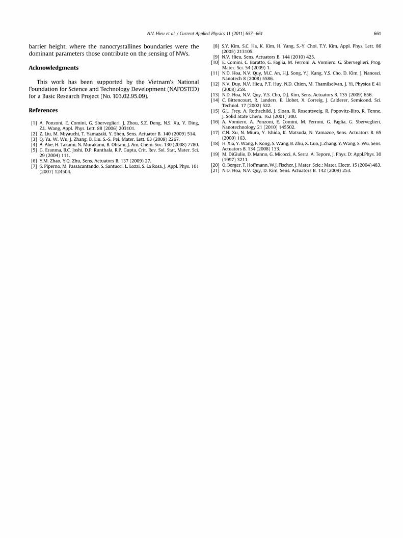
Fig. 4. The schematic illustration of gas sensing mechanism of WO3 NWs.
N.V. Hieu et al. / Current Applied Physics 11 (2011) 657e661660
scale. It can be seen that the temperature has an obvious influenceon the response of sensors to NH3 gas. The sensor exhibits a highestresponse at aworking temperature of 250 �C, inwhich the responsesare 2.39, 3.12, 3.80, 7.20, and 9.67 for 300, 400, 500, 1000, and1500 ppm NH3 concentration, respectively. The relationshipbetween the sensor response and NH3 gas concentration issummarized in Fig. 2(e). The response linearly increases as a func-tion of NH3 gas concentration in themeasured range (from300 ppmto1500 ppm). Linear dependence of response and gas concentrationis an advantage for designing read out signal circuits.
For practical applications, the response and recovery times of thegas sensors are highly important issues. Fig. 3 shows the plots of thedynamic responses at a tested temperature to 500ppmNH3 gas. Theresponse time for gas exposure [t90%(air-to-gas)] and that for recovery[t90%(gas-to-air)] were calculated from the response-time data shownin Fig. 3. The t90%(air-to-gas) values at operating temperature of 200,250 and 300 �C are around 16, 7 and 15 s, respectively, whereas thet90%(gas-to-air) values at operating temperature of 200, 250 and 300 �Care around 16, 8 and 13 s, respectively. Our WO3 NWs sensors showrelatively fast response and recovery times (about 10 s). These valuesaremore significant if noticing that the response and recovery timesreported by other researchers are in the range of from 1 min to10 min [17]. In this work, we used high-speed switching gaschamber, detail was described in ref. [12]. The purge/filling timewasabout 3e5 s. Therefore, the rapid response and recovery of oursensors are due to the porosity of the NWs sensors and the use ofhigh-speed switching gas chamber. Indeed, the porosityof NWs thinfilm enables gas molecules easily penetrate and adsorb on thesurface of NWs, deceasing the response time. The high-speedswitching gas chamber accelerates the purge/filling process andtherefore decreases the response and recovery time.
OurWO3NWis formed fromnanocrystallines linked together (seeTEM images). Therefore, the gas sensing mechanism of our sensorscan be explained by using surface resistivity and barrier heightmodelas illustrated in Fig. 4. When n-type semiconducting tungsten oxideNWs are exposed to air, the oxygen molecules in air adsorb on thesurface of WO3 (in the form of O�
2 , O�, or O2�) [18] and withdraw
electrons fromNWs leading to the formation of an electron depletionlayer [5]. The depth of the depletion layer (or space charge region) isestimated by theDebye-length L ¼ ð33okBT=e2nbÞ1=2, where nb is thebulk carrierdensity, T is the absolute temperature, kB is theBoltzmannconstant, e is the electron charge, 3 is the dielectric constant of WO3,and 3o is the dielectric permittivity of vacuum [6]. We could notmeasure the carrier density of our WO3 NWs. However, we
260 280 300 320 340 360 380 400 420
1.0
1.5
2.0
2.5
3.0
3.5
4.0
4.5
5.0
90%(gas-to-air)~ 13 st90%(air-to-gas)~15 s
t90%(gas-to-air)~ 16 s
t90%(gas-to-air)~ 8st90%(air-to-gas)~ 7 s
t90%(air-to-gas)~17 s
@200oC
@300oC
Re
sp
on
se
(R
air/R
ga
s)
Time(s)
@250oC
500 ppm NH3
Fig. 3. The response transient of WO3 NWs sensor to 500 ppm NH3 gas for calculationof response-recovery time at operating temperatures of 200, 250 and 300 �C.
considered that the carrier density of WO3 thin film fabricated bysputteringmethod is in the range of 4.0� 1015e4.0� 1016 cm�3 [19].Naturally, we cannot directly use this value as the carrier density forour WO3 NWs because this value depends on the density of oxygenvacancies in the NWs. However, as a reference, the Debye-lengthcalculated for temperature of 250 �C using nb ¼ 4.0 � 1015 cm�3 isabout 11 nm, which is much smaller than the radius (35 nm) of WO3NWs. Therefore, the gas sensing mechanism of our WO3 NWs obeysShottky-barrier-controlled model [20]. Note that the WO3 NW isformed from linked nanocrystallines; thus, the depletion layergenerates an energy barrier at the boundary between nanocrystal-lines (Fig. 4). When exposed to ammonia gas, the NH3 moleculesinteract with pre-adsorbed oxygen and release electrons to WO3NWs. The interaction of ammonium molecules and pre-adsorbedoxygen on the surface of WO3 NWs is indicated in Eqs. (1)e(4):
NH3ðgasÞ4NH3ðadsÞ (1)
2NH3ðadsÞ þ 3=2O�2 ðadsÞ4N2 þ 3H2Oþ 3e� (2)
2NH3ðadsÞ þ 3O�ðadsÞ4N2 þ 3H2Oþ 3e� (3)
2NH3ðadsÞ þ 3O2�ðadsÞ4N2 þ 3H2Oþ 6e� (4)
The free electrons released from Eqs. (1)e(4) increase the carrierin WO3 NWs resulting in (i) a decrease in the surface resistivity ofWO3 NWs and (ii) a decrease in the barrier height DVS at theboundary between nanocrystallines along the NW. The change inresistance due to the decrease in barrier height DVS is described asRgaswRairexpð�eDVS=kBTÞ [21]. According to the exponentialfunction of DVS the change in resistance (and response) is consid-erably more evident compared with others, suggesting thatparameter (ii) is most likely the dominant parameter control in thesensing mechanisms of our NWs.
4. Conclusion
We have introduced a facile and scaleable method for synthe-sizing WO3 NWs using SWCNTs as templates. The synthesizedWO3NWs are smooth with single crystal but are formed from linkednanocrystallines. This nanowires structure is excellent for gassensor application. TheWO3 NWs sensor shows very high responseto NH3 with fast response and recovery times (in seconds). Thelinear dependence of sensor response on NH3 concentration in themeasured range indicates promising potential for practical appli-cation. In addition, the sensing mechanism of the present WO3samples was discussed in the framework of surface resistivity and
N.V. Hieu et al. / Current Applied Physics 11 (2011) 657e661 661
barrier height, where the nanocrystallines boundaries were thedominant parameters those contribute on the sensing of NWs.
Acknowledgments
This work has been supported by the Vietnam’s NationalFoundation for Science and Technology Development (NAFOSTED)for a Basic Research Project (No. 103.02.95.09).
References
[1] A. Ponzoni, E. Comini, G. Sberveglieri, J. Zhou, S.Z. Deng, N.S. Xu, Y. Ding,Z.L. Wang, Appl. Phys. Lett. 88 (2006) 203101.
[2] Z. Liu, M. Miyauchi, T. Yamazaki, Y. Shen, Sens. Actuator B. 140 (2009) 514.[3] Q. Ya, W. Wu, J. Zhang, B. Liu, S.-S. Pei, Mater. Lett. 63 (2009) 2267.[4] A. Abe, H. Takami, N. Murakami, B. Ohtani, J. Am, Chem. Soc. 130 (2008) 7780.[5] G. Eranma, B.C. Joshi, D.P. Runthala, R.P. Gupta, Crit. Rev. Sol. Stat, Mater. Sci.
29 (2004) 111.[6] Y.M. Zhao, Y.Q. Zhu, Sens. Actuators B. 137 (2009) 27.[7] S. Piperno, M. Passacantando, S. Santucci, L. Lozzi, S. La Rosa, J. Appl. Phys. 101
(2007) 124504.
[8] S.Y. Kim, S.C. Ha, K. Kim, H. Yang, S.-Y. Choi, T.Y. Kim, Appl. Phys. Lett. 86(2005) 213105.
[9] N.V. Hieu, Sens. Actuators B. 144 (2010) 425.[10] E. Comini, C. Baratto, G. Faglia, M. Ferroni, A. Vomiero, G. Sberveglieri, Prog.
Mater. Sci. 54 (2009) 1.[11] N.D. Hoa, N.V. Quy, M.C. An, H.J. Song, Y.J. Kang, Y.S. Cho, D. Kim, J. Nanosci,
Nanotech 8 (2008) 5586.[12] N.V. Duy, N.V. Hieu, P.T. Huy, N.D. Chien, M. Thamilselvan, J. Yi, Physica E 41
(2008) 258.[13] N.D. Hoa, N.V. Quy, Y.S. Cho, D.J. Kim, Sens. Actuators B. 135 (2009) 656.[14] C. Bittencourt, R. Landers, E. Llobet, X. Correig, J. Calderer, Semicond. Sci.
Technol. 17 (2002) 522.[15] G.L. Frey, A. Rothschild, J. Sloan, R. Rosentsveig, R. Popovitz-Biro, R. Tenne,
J. Solid State Chem. 162 (2001) 300.[16] A. Vomiero, A. Ponzoni, E. Comini, M. Ferroni, G. Faglia, G. Sberveglieri,
Nanotechnology 21 (2010) 145502.[17] C.N. Xu, N. Miura, Y. Ishida, K. Matsuda, N. Yamazoe, Sens. Actuators B. 65
(2000) 163.[18] H. Xia, Y. Wang, F. Kong, S. Wang, B. Zhu, X. Guo, J. Zhang, Y. Wang, S. Wu, Sens.
Actuators B. 134 (2008) 133.[19] M. DiGiulio, D. Manno, G. Micocci, A. Serra, A. Tepore, J. Phys. D: Appl.Phys. 30
(1997) 3211.[20] O. Berger, T. Hoffmann,W.J. Fischer, J. Mater. Scie.: Mater. Electr. 15 (2004) 483.[21] N.D. Hoa, N.V. Quy, D. Kim, Sens. Actuators B. 142 (2009) 253.


![Trabalho NH3[1]](https://img.pdfslide.net/doc/110x75/5571f9ee497959916990cc2a/trabalho-nh31.jpg)