Embed Size (px)
Citation preview

Presented at: The International Conference and Exhibition on High Density Interconnect and Systems Packaging
Santa Clara, California, April 20th, 2001
Best of Session Award
Slide 1
M icroSound/ESI
HD International, Santa Clara, CA
A High-Density, Resin-Coated-Foil (RCF) Substrate Utilizing Mask and Direct-Write UV Laser
Photolithography
Scott Corbett*, Edward Swenson**, Jeff Strole*, Bill Beck*, John Yarno*, Thayer Hughes***
*MicroSound Systems, Inc.**ElectroScientific Industries, Inc.

Presented at: The International Conference and Exhibition on High Density Interconnect and Systems Packaging
Santa Clara, California, April 20th, 2001
Best of Session Award
Slide 2
M icroSound/ESI
Resin Coated Foil (RCF) buildup circuits provide solution for HDI
circuit boards:
• Laser-drillable dielectric
• Good planarity/thin metalization supports fine-line patterning.
• Compatible with existing board processes

Presented at: The International Conference and Exhibition on High Density Interconnect and Systems Packaging
Santa Clara, California, April 20th, 2001
Best of Session Award
Slide 3
M icroSound/ESI
FR4 Layer
RCF Layer 1
RCF Layer 2
Laser drilledvias
Typical RCF Buildup circuit:

Presented at: The International Conference and Exhibition on High Density Interconnect and Systems Packaging
Santa Clara, California, April 20th, 2001
Best of Session Award
Slide 4
M icroSound/ESI
HDI Buildup Circuit Issues:
•Trace/space smaller than 50µm/50µm requires expensive imaging and processing equipment
•Direct write imagers one answer to fine-line lithography but are there other solutions?

Presented at: The International Conference and Exhibition on High Density Interconnect and Systems Packaging
Santa Clara, California, April 20th, 2001
Best of Session Award
Slide 5
M icroSound/ESI
Advantages of Direct-Write
•Finer trace/space
•“Virtual” pattern can be scaled to match part geometry based on fiducial alignment
Disadvantages of Direct-Write
•Dedicated equipment and process materials required
•Slower throughput
•Potential raster image problems at small trace widths

Presented at: The International Conference and Exhibition on High Density Interconnect and Systems Packaging
Santa Clara, California, April 20th, 2001
Best of Session Award
Slide 6
M icroSound/ESI
Can Direct-Write be combined with Conventional Mask Imaging?
•Best of both worlds
– Use mask for large area exposure
– Use direct-write for fine detail exposure and precise alignment in select regions (ie. PGA layout region)
•However…..
– Direct-write process must be compatible with existing photomask resists and process methods

Presented at: The International Conference and Exhibition on High Density Interconnect and Systems Packaging
Santa Clara, California, April 20th, 2001
Best of Session Award
Slide 7
M icroSound/ESI
Is a UV laser-drill suitable for direct-write imaging?
•355 nm wavelength same as required for resist exposure (tripled-YAG)
•Vector control of beam position
•Automatic control of laser fluence down to 30mJ/cm2 (1-5 mW average power) in range required for resist exposure or ablation
•Serves dual purpose of drilling and patterning

Presented at: The International Conference and Exhibition on High Density Interconnect and Systems Packaging
Santa Clara, California, April 20th, 2001
Best of Session Award
Slide 8
M icroSound/ESI
Our process development tool:ESI 5200 UV laser drill
enables new interconnect architectures:
• Flexible pulse and power control
• Direct write ablation
• Non contact machining
• Non-rectilinear patterns
• Via drilling through die
• Direct-write photolithography
Tripled-YAG technology

Presented at: The International Conference and Exhibition on High Density Interconnect and Systems Packaging
Santa Clara, California, April 20th, 2001
Best of Session Award
Slide 9
M icroSound/ESI
Two potential approaches to UV laser direct-writing of photoresist:
•Resist exposure (low fluence level)
•Resist ablation (higher fluence, but still significantly lower than dielectric drilling)
Process compatible with:
– Positive or negative photoresist– Subtractive or additive process

Presented at: The International Conference and Exhibition on High Density Interconnect and Systems Packaging
Santa Clara, California, April 20th, 2001
Best of Session Award
Slide 10
M icroSound/ESI
Laser Exposure versus Ablation(Negative Resist Example)
Laser Exposure(Pattern traces)
Laser
Laser Ablation(Pattern spaces)
ResistMetalizationDielectric

Presented at: The International Conference and Exhibition on High Density Interconnect and Systems Packaging
Santa Clara, California, April 20th, 2001
Best of Session Award
Slide 11
M icroSound/ESI
Detail of Resist Ablation
Top of resist Bottom of resist12 µm 8 µm

Presented at: The International Conference and Exhibition on High Density Interconnect and Systems Packaging
Santa Clara, California, April 20th, 2001
Best of Session Award
Slide 12
M icroSound/ESI
Detail of Resist Ablation Showing Effect of Gaussian Beam:

Presented at: The International Conference and Exhibition on High Density Interconnect and Systems Packaging
Santa Clara, California, April 20th, 2001
Best of Session Award
Slide 13
M icroSound/ESI
Etched part:(10 micron trace/20 micron space)

Presented at: The International Conference and Exhibition on High Density Interconnect and Systems Packaging
Santa Clara, California, April 20th, 2001
Best of Session Award
Slide 14
M icroSound/ESI
Etched Line Pattern from Resist Exposure Process

Presented at: The International Conference and Exhibition on High Density Interconnect and Systems Packaging
Santa Clara, California, April 20th, 2001
Best of Session Award
Slide 15
M icroSound/ESI
SEM Detail of UV Laser Direct-Write Lithography Pattern
(using spin-on negative resist and laser exposure process)

Presented at: The International Conference and Exhibition on High Density Interconnect and Systems Packaging
Santa Clara, California, April 20th, 2001
Best of Session Award
Slide 16
M icroSound/ESI
5310 Optics Schematic
UV Laser
Collimator
BeamShaper
Imaging Galvos Scan Lens
Sample
ZBE

Presented at: The International Conference and Exhibition on High Density Interconnect and Systems Packaging
Santa Clara, California, April 20th, 2001
Best of Session Award
Slide 17
M icroSound/ESI
Via Via -- Top Diameter 18 µm Top Diameter 18 µm and Bottom Diameter 12 µm and Bottom Diameter 12 µm

Presented at: The International Conference and Exhibition on High Density Interconnect and Systems Packaging
Santa Clara, California, April 20th, 2001
Best of Session Award
Slide 18
M icroSound/ESI
Putting it all together to build an HDI substrate
•Fabricated two-layer, RCF buildup circuit on FR4 substrate (Polyclad CF400, C25T/B35T)
•Combined mask exposure and laser direct write lithography (exposure process)

Presented at: The International Conference and Exhibition on High Density Interconnect and Systems Packaging
Santa Clara, California, April 20th, 2001
Best of Session Award
Slide 19
M icroSound/ESI
PGA Redistribution Pattern (top layer)
1 1
White region-mask exposureRed region- laser exposure
Presented at: The International Conference and Exhibition on High Density Interconnect and Systems Packaging
Santa Clara, California, April 20th, 2001
Best of Session Award
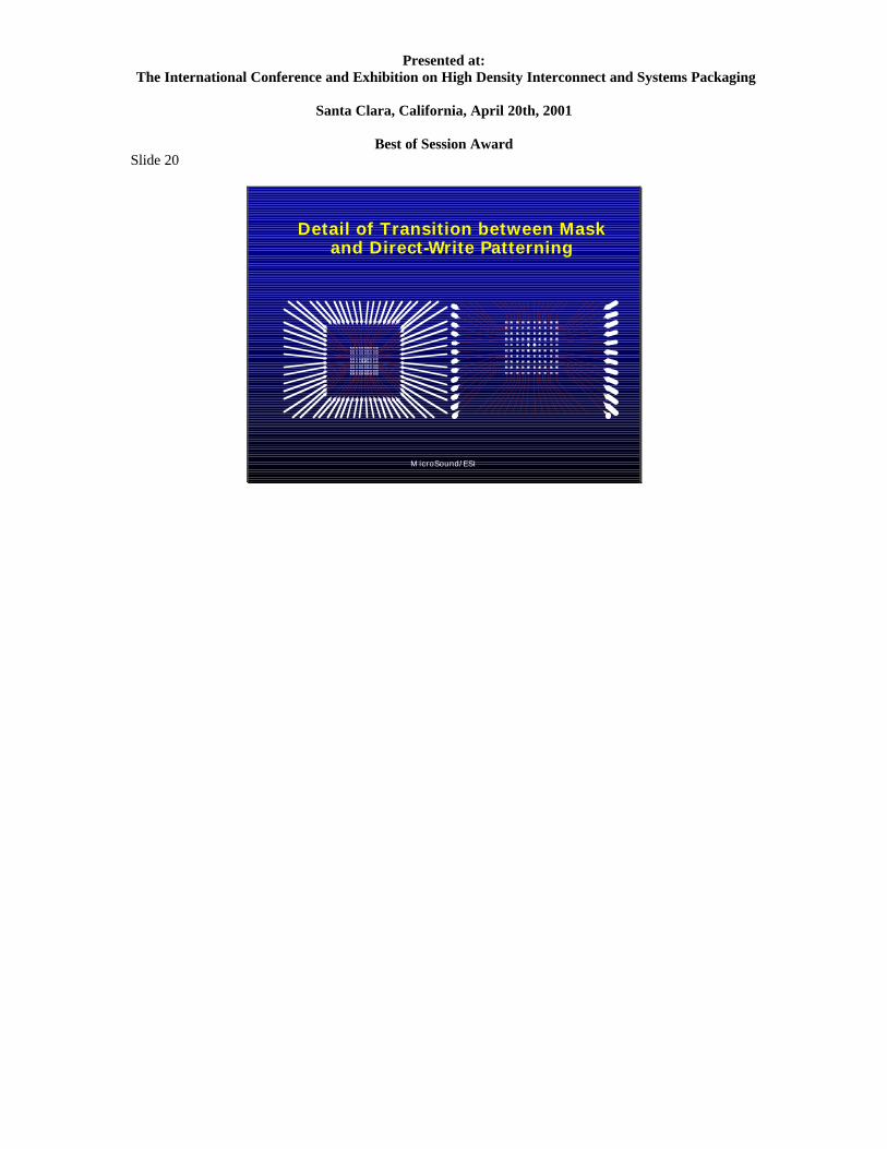
Slide 20
M icroSound/ESI
Detail of Transition between Mask and Direct-Write Patterning

Presented at: The International Conference and Exhibition on High Density Interconnect and Systems Packaging
Santa Clara, California, April 20th, 2001
Best of Session Award
Slide 21
M icroSound/ESI
Completed Part:Detail of Laser Direct-Write Region

Presented at: The International Conference and Exhibition on High Density Interconnect and Systems Packaging
Santa Clara, California, April 20th, 2001
Best of Session Award
Slide 22
M icroSound/ESI
Combined Mask/Exposure Process Details:
• Laminate RCF Foil
• Laser drill vias
• Plate vias
• Apply resist film
• Pattern resist using mask exposure (mask opaque in laser direct-write regions)
• Further expose resist in fine-line regions using laser direct-write process
• Develop out resist
• Process using subtractive etching
• Strip resist

Presented at: The International Conference and Exhibition on High Density Interconnect and Systems Packaging
Santa Clara, California, April 20th, 2001
Best of Session Award
Slide 23
M icroSound/ESI
Summary
•Demonstrated use of UV laser drill as Direct-Write Imager
•Demonstrated both exposure and ablation of standard dry film resist
•Demonstrated combined mask/laser-write process (18µm trace in laser region)
•Application for high density HDI circuits for fine line patterning in array interconnect regions
www.microsnd.com www.esi.com