Embed Size (px)
Citation preview
Direct-Write of Sensor Devices by a Laser Forward Transfer Technique
A. Piquéa*, D.W. Weira, P.K. Wub, B. Pratapa, C.B. Arnolda, B.R. Ringeisena,R.A. McGilla, R.C.Y. Auyeunga, R.A. Kanta and D.B. Chriseya
aNaval Research Laboratory, Washington, DC 20375bDepartment of Physics, Southern Oregon University, OR 97520
ABSTRACT
The use of direct-write techniques in the design and manufacture of sensor devices provides a flexible approach for nextgeneration commercial and defense sensor applications. Using a laser forward transfer technique, we have demonstrated theability to rapidly prototype temperature, biological and chemical sensor devices. This process, known as matrix assistedpulsed laser evaporation direct-write or MAPLE DW is compatible with a broad class of materials ranging from metals andelectronic ceramics to chemoselective polymers and biomaterials. Various types of miniature sensor designs have beenfabricated incorporating different materials such as metals, polymers, biomaterials or composites as multilayers or discretestructures on a single substrate. The MAPLE DW process is computer controlled which allows the sensor design to beeasily modified and adapted to any specific application. To illustrate the potential of this technique, a functional chemicalsensor system is demonstrated by fabricating all the passive and sensor components by MAPLE DW on a polyimidesubstrate. Additional devices fabricated by MAPLE DW including biosensors and temperature sensors and theirperformance are shown to illustrate the breadth of MAPLE DW and how this technique may influence current and futuresensor applications.
Keywords: MAPLE Direct-Write, Laser Transfer, Direct-Write of Sensor Materials, Temperature Sensors, BiologicalSensors, Chemical Sensors, Chemiresistor.
1. INTRODUCTION
Current trends for developing advanced electronic and sensor systems place great emphasis in achieving performance levelsgenerally associated with integrated circuits. This requires further miniaturization, while enhancing the functionality andreliability of existing components. It also requires new strategies in order to eliminate the long lead times required for thefabrication of prototypes and evaluation of new materials and designs. In particular, for chemical and biological sensordevelopment, the trend is toward the fabrication of micron scale devices and dense array platforms1.
An individual chemical or biological sensor element consists of a transducer or substrate coated with one of a range ofsorbent coating materials that collect the analyte of interest either in a reversible or irreversible binding process.Physicochemical changes in the sorbent coating, as a result of analyte binding events, are monitored and converted toelectrical signals for display or recording. The range of sorbent materials covers a plethora of types and properties fromsimple polymers to higher-ordered biological structures. In order for these materials to perform as expected, their chemicaland structural properties must remain uncompromised during the manufacture of the sensor1. In addition to the materialsconstraints, current commercial and military applications for chemical and biological sensors require systems to be portable(hand-held or smaller in size) so that analytical measurements can be made in the field. The above requirements havepushed traditional manufacturing techniques to their limits. Novel fabrication approaches for integrated micron sized sensorelements and systems are required.
* Correspondence: Email: [email protected]; Telephone: (202) 767 5653; Fax: (202) 767 5301
2
The use of direct-write techniques, that do not need photolithographic processing, provide a solution to the aboveconstraints. Direct-write technologies do not compete with photolithography for size and scale, but rather add acomplementary tool for specific applications requiring rapid turnaround and/or pattern iteration, conformal patterning, orfor modeling difficult circuits2. Examples of direct-write technologies for fabricating or modifying metallic interconnectsand/or other electronic passive elements include ink jet printing3, direct-write of ceramic slurries (Micropen©)4, lasertrimming5 and laser chemical vapor deposition (LCVD)6. However, none of the above techniques is capable of operating inair and at room temperature while maintaining sub-10 µm resolution and without requiring ex situ processing. Furthermore,multiple techniques are necessary to deposit and process the broad classes of materials employed in electronic and sensorapplications.
Over the past decade, various laser-based direct-write techniques have been developed for depositing different types ofmaterials such as metals for interconnects and mask repair. More recently, a new laser-based direct-write technique, calledMAPLE DW, for Matrix-Assisted Pulsed-Laser Evaporation Direct-Write, has been used for the direct-write of conformalelectronic devices7-10, phosphor materials11, microbatteries12,13 and even viable biomaterials14,15. In this paper, the use of theMAPLE DW technique for the fabrication of temperature, biological and chemical sensors is described. We compare theperformance of chemiresistor gas sensors made by spray coating and by MAPLE DW. Finally, we demonstrate a completechemical sensor system fabricated by MAPLE DW
2. BACKGROUND
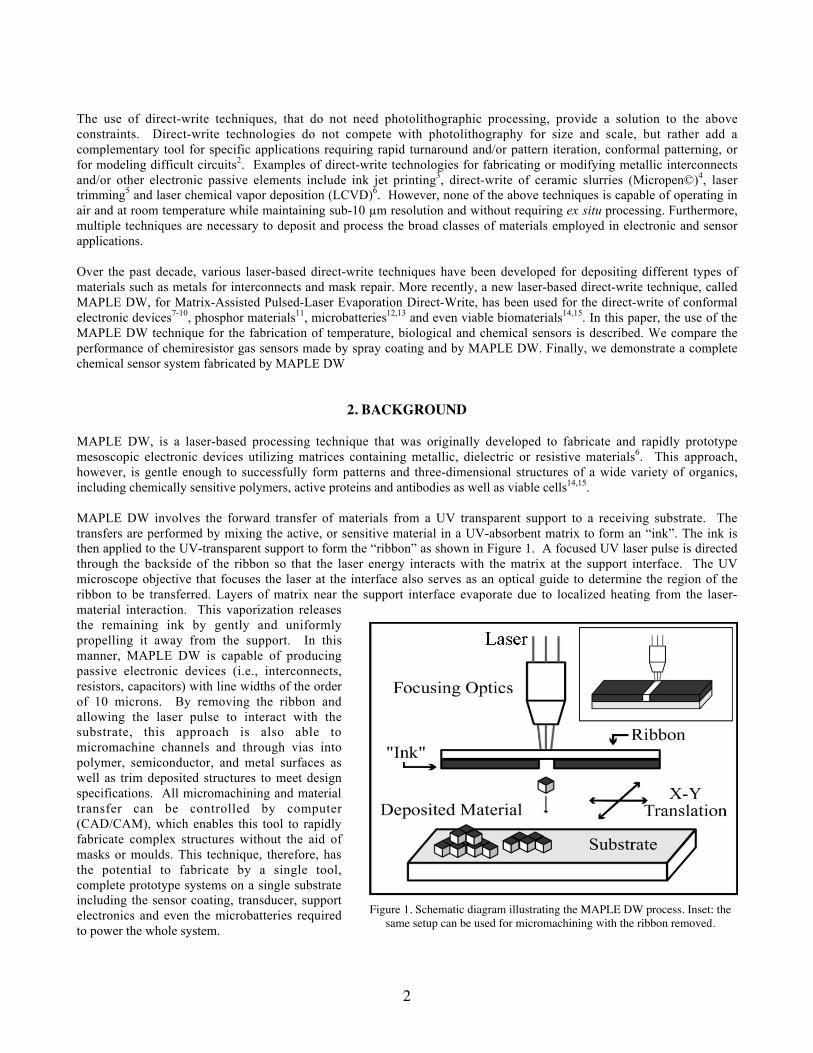
MAPLE DW, is a laser-based processing technique that was originally developed to fabricate and rapidly prototypemesoscopic electronic devices utilizing matrices containing metallic, dielectric or resistive materials6. This approach,however, is gentle enough to successfully form patterns and three-dimensional structures of a wide variety of organics,including chemically sensitive polymers, active proteins and antibodies as well as viable cells14,15.
MAPLE DW involves the forward transfer of materials from a UV transparent support to a receiving substrate. Thetransfers are performed by mixing the active, or sensitive material in a UV-absorbent matrix to form an “ink”. The ink isthen applied to the UV-transparent support to form the “ribbon” as shown in Figure 1. A focused UV laser pulse is directedthrough the backside of the ribbon so that the laser energy interacts with the matrix at the support interface. The UVmicroscope objective that focuses the laser at the interface also serves as an optical guide to determine the region of theribbon to be transferred. Layers of matrix near the support interface evaporate due to localized heating from the laser-material interaction. This vaporization releasesthe remaining ink by gently and uniformlypropelling it away from the support. In thismanner, MAPLE DW is capable of producingpassive electronic devices (i.e., interconnects,resistors, capacitors) with line widths of the orderof 10 microns. By removing the ribbon andallowing the laser pulse to interact with thesubstrate, this approach is also able tomicromachine channels and through vias intopolymer, semiconductor, and metal surfaces aswell as trim deposited structures to meet designspecifications. All micromachining and materialtransfer can be controlled by computer(CAD/CAM), which enables this tool to rapidlyfabricate complex structures without the aid ofmasks or moulds. This technique, therefore, hasthe potential to fabricate by a single tool,complete prototype systems on a single substrateincluding the sensor coating, transducer, supportelectronics and even the microbatteries requiredto power the whole system.
Figure 1. Schematic diagram illustrating the MAPLE DW process. Inset: thesame setup can be used for micromachining with the ribbon removed.
3
3. EXPERIMENTAL
3.1 MAPLE DW Ribbon Preparation
Borosilicate glass discs, double side polished, 5.0 cm diameter x 3mm thick were used as ribbon supports. For thefabrication of the temperature sensors, a screen printable silver paste (Parmod RRA-100, from Paralec, Inc.) was applied toone side of the discs using a #4 wire-coater (Gardner, Inc.) to form an ink layer about 15 µm thick. For the fabrication ofthe biosensor, a paste containing polyphenol oxidase, graphite and mineral oil was applied using the same wire-coater. Inthe case of the chemical sensors, the ribbons were prepared by spray coating a solution containing 0.1 gm ofpolyepichlorohydrin (PECH, average MW = 700000, Aldrich) and 0.01 gm of acetylene carbon black (Alfa) mixed in 50 mlof chloroform. The coated side of the ribbons was kept at a distance of 100-200 µm from the substrate with a spacer. Boththe substrate and the ribbon were held in place using a vacuum chuck over the X-Y substrate translation stage. The thirdharmonic emission of a Nd:YAG laser, λ = 355 nm (Spectra Physics), was directed through a circular aperture and a 10xobjective lens, resulting in a 85 µm diameter spot at the ribbon. The laser fluence varied between 0.1 – 1.0 J/cm2 dependingon the material being transferred, and was estimated by averaging the total energy of the incident beam over the irradiatedarea.
3.2 Temperature sensor fabrication and testing
Silver conductive lines were transferred by MAPLE DW onto polyimide substrates and used as temperature sensors. Thelength and layout of the lines was easily modified via computer control in order to achieve ~ 10-µm thick and ~ 100-µmwide patterns. The silver ink was dried at 100 °C on a hot plate to remove excess solvent and then cured at 280 °C in anoven for 10 min to decompose the organic silver precursors in order to form conductive patterns. These patterns in the formof serpentine lines were evaluated as temperature sensors by comparing their response to that of a type K thermocouple.One of the MAPLE DW serpentine patterns and a thermocouple were mounted next to each other and exposed to heatpulses generated by a heat gun over a temperature range of 24 to 60 °C. The resistance of the serpentine was measured as afunction of time using a computer controlled 34401A digital multimeter (Agilent).
3.3 Biosensor fabrication and testing
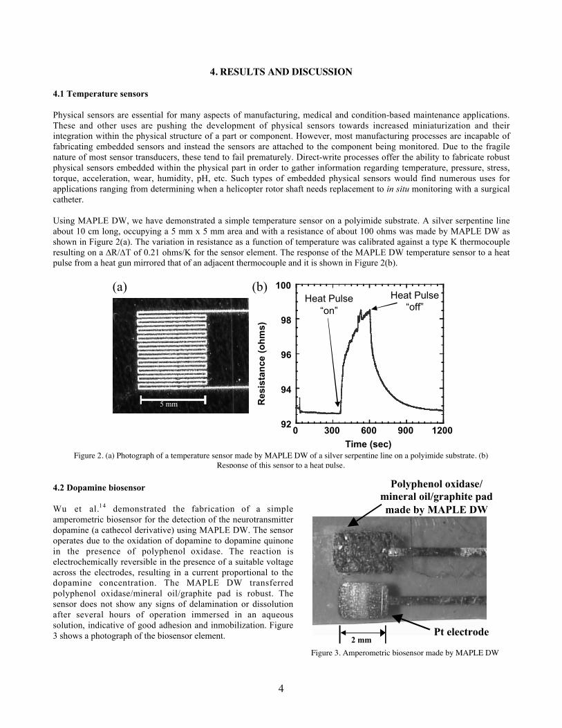
A 2 mm x 2 mm pad containing the biosensor mixture of polyphenol oxidase/mineral oil/graphite was deposited byMAPLE DW over Pt electrodes on a polyimide substrate. The resulting biosensor was immersed in a cathecol/watersolution in order to measure the current generated across the Pt electrodes by the electrochemical reaction between thepolyphenol oxidase and the cathecol. Details of the measurement are provided elsewhere14. Cyclic voltammetrymeasurements were performed using a PAR 263 potentiostat (EG&G) driven with M270 software.
3.4 Chemical sensor fabrication and testing
For the chemical sensors, 1 mm x 4 mm pads of PECH/carbon were deposited by MAPLE DW over silver interdigitatedelectrodes. To verify the operation of the MAPLE DW sensors, similar pads of PECH/carbon were spray coated onto asecond set of silver electrodes. The silver electrodes were deposited by MAPLE DW onto polyimide substrates in the sameway as the serpentine lines. The response of the PECH/carbon sensors was evaluated by exposing them to controlledexposures of toluene and dimethylmethylphosphonate (DMMP) vapor streams. The carrier air temperature and humiditywere controlled with a Miller Nelson HCS-301 air-humidity generator. An automated Harvard 22 liquid syringe pumpsystem was utilized to generate analyte vapor by injecting the liquid analyte into a heated evaporation plate system. Theresulting vapor was mixed with humidified carrier air and passed into a test chamber housing the chemical sensors. The testchamber consisted of a hermetic enclosure with opposite inlet and outlet gas ports, to allow vapor flow over the sensors.The chemical integrity of the PECH polymer transfers was verified by FTIR using a Magna-IR 750 spectrophotometer(Nicolet). The spectra from 4 mm x 4 mm pads of pure PECH (no carbon) deposited by MAPLE DW onto NaCl discs wascompared to that of a PECH films spray coated from a solution of PECH in chloroform.
4
4. RESULTS AND DISCUSSION
4.1 Temperature sensors
Physical sensors are essential for many aspects of manufacturing, medical and condition-based maintenance applications.These and other uses are pushing the development of physical sensors towards increased miniaturization and theirintegration within the physical structure of a part or component. However, most manufacturing processes are incapable offabricating embedded sensors and instead the sensors are attached to the component being monitored. Due to the fragilenature of most sensor transducers, these tend to fail prematurely. Direct-write processes offer the ability to fabricate robustphysical sensors embedded within the physical part in order to gather information regarding temperature, pressure, stress,torque, acceleration, wear, humidity, pH, etc. Such types of embedded physical sensors would find numerous uses forapplications ranging from determining when a helicopter rotor shaft needs replacement to in situ monitoring with a surgicalcatheter.
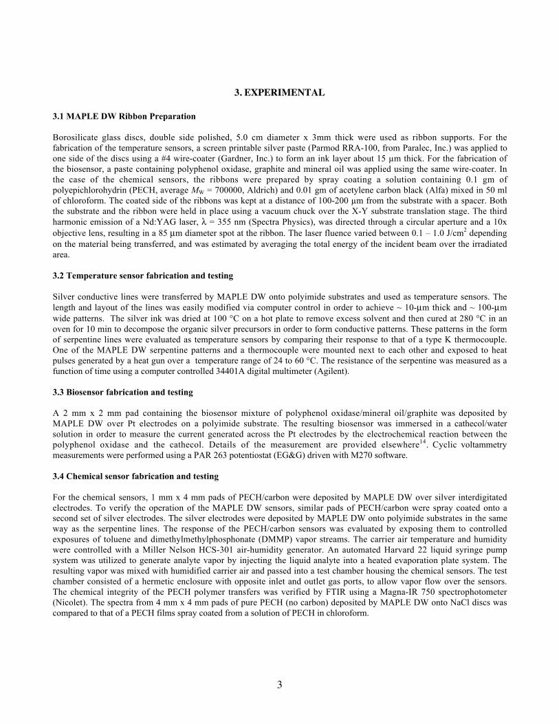
Using MAPLE DW, we have demonstrated a simple temperature sensor on a polyimide substrate. A silver serpentine lineabout 10 cm long, occupying a 5 mm x 5 mm area and with a resistance of about 100 ohms was made by MAPLE DW asshown in Figure 2(a). The variation in resistance as a function of temperature was calibrated against a type K thermocoupleresulting on a ∆R/∆T of 0.21 ohms/K for the sensor element. The response of the MAPLE DW temperature sensor to a heatpulse from a heat gun mirrored that of an adjacent thermocouple and it is shown in Figure 2(b).
4.2 Dopamine biosensor
Wu et al.1 4 demonstrated the fabrication of a simpleamperometric biosensor for the detection of the neurotransmitterdopamine (a cathecol derivative) using MAPLE DW. The sensoroperates due to the oxidation of dopamine to dopamine quinonein the presence of polyphenol oxidase. The reaction iselectrochemically reversible in the presence of a suitable voltageacross the electrodes, resulting in a current proportional to thedopamine concentration. The MAPLE DW transferredpolyphenol oxidase/mineral oil/graphite pad is robust. Thesensor does not show any signs of delamination or dissolutionafter several hours of operation immersed in an aqueoussolution, indicative of good adhesion and inmobilization. Figure3 shows a photograph of the biosensor element.
92
94
96
98
100
0 300 600 900 1200
Res
ista
nce
(o
hm
s)
Time (sec)
Heat Pulse“off”
Heat Pulse“on”
(b)
5 mm
(a)
Figure 2. (a) Photograph of a temperature sensor made by MAPLE DW of a silver serpentine line on a polyimide substrate. (b)Response of this sensor to a heat pulse.
2 mm
Polyphenol oxidase/mineral oil/graphite padmade by MAPLE DW
Pt electrode
Figure 3. Amperometric biosensor made by MAPLE DW
5
4.3 Chemiresistor gas sensors
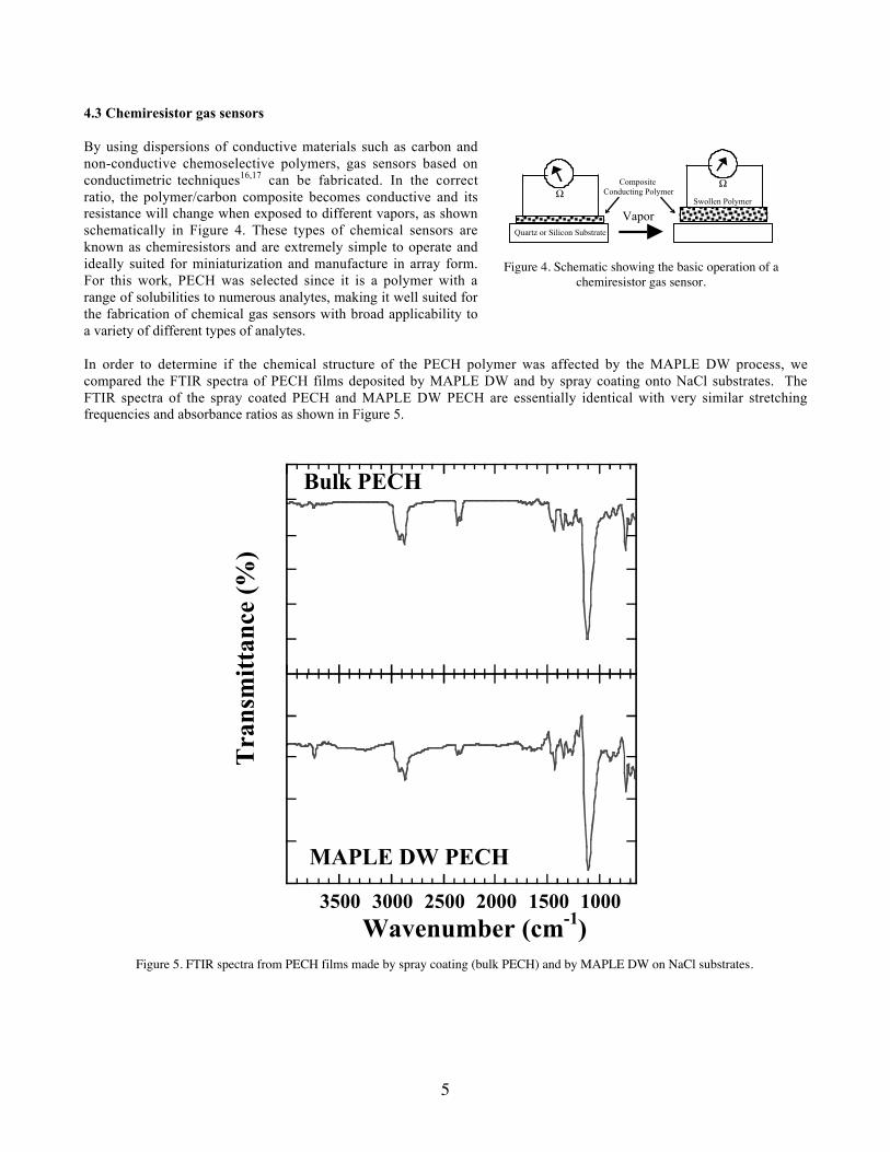
By using dispersions of conductive materials such as carbon andnon-conductive chemoselective polymers, gas sensors based onconductimetric techniques16,17 can be fabricated. In the correctratio, the polymer/carbon composite becomes conductive and itsresistance will change when exposed to different vapors, as shownschematically in Figure 4. These types of chemical sensors areknown as chemiresistors and are extremely simple to operate andideally suited for miniaturization and manufacture in array form.For this work, PECH was selected since it is a polymer with arange of solubilities to numerous analytes, making it well suited forthe fabrication of chemical gas sensors with broad applicability toa variety of different types of analytes.
In order to determine if the chemical structure of the PECH polymer was affected by the MAPLE DW process, wecompared the FTIR spectra of PECH films deposited by MAPLE DW and by spray coating onto NaCl substrates. TheFTIR spectra of the spray coated PECH and MAPLE DW PECH are essentially identical with very similar stretchingfrequencies and absorbance ratios as shown in Figure 5.
SAW Sensor SAW SensorQuartz or Silicon Substrate
Swollen Polymer
Vapor
Composite Conducting PolymerΩ
Ω
Figure 4. Schematic showing the basic operation of achemiresistor gas sensor.
100015002000250030003500
Wavenumber (cm-1)
Transmittan
Bulk PECH
MAPLE DW PECH
Tra
nsm
itta
nce
(%)
Figure 5. FTIR spectra from PECH films made by spray coating (bulk PECH) and by MAPLE DW on NaCl substrates.
6
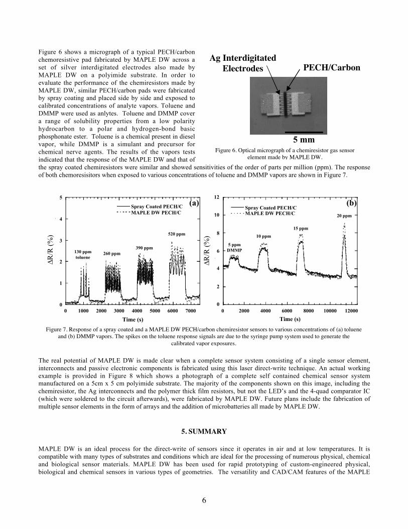
Figure 6 shows a micrograph of a typical PECH/carbonchemoresistive pad fabricated by MAPLE DW across aset of silver interdigitated electrodes also made byMAPLE DW on a polyimide substrate. In order toevaluate the performance of the chemiresistors made byMAPLE DW, similar PECH/carbon pads were fabricatedby spray coating and placed side by side and exposed tocalibrated concentrations of analyte vapors. Toluene andDMMP were used as anlytes. Toluene and DMMP covera range of solubility properties from a low polarityhydrocarbon to a polar and hydrogen-bond basicphosphonate ester. Toluene is a chemical present in dieselvapor, while DMMP is a simulant and precursor forchemical nerve agents. The results of the vapors testsindicated that the response of the MAPLE DW and that ofthe spray coated chemiresistors were similar and showed sensitivities of the order of parts per million (ppm). The responseof both chemoresisitors when exposed to various concentrations of toluene and DMMP vapors are shown in Figure 7.
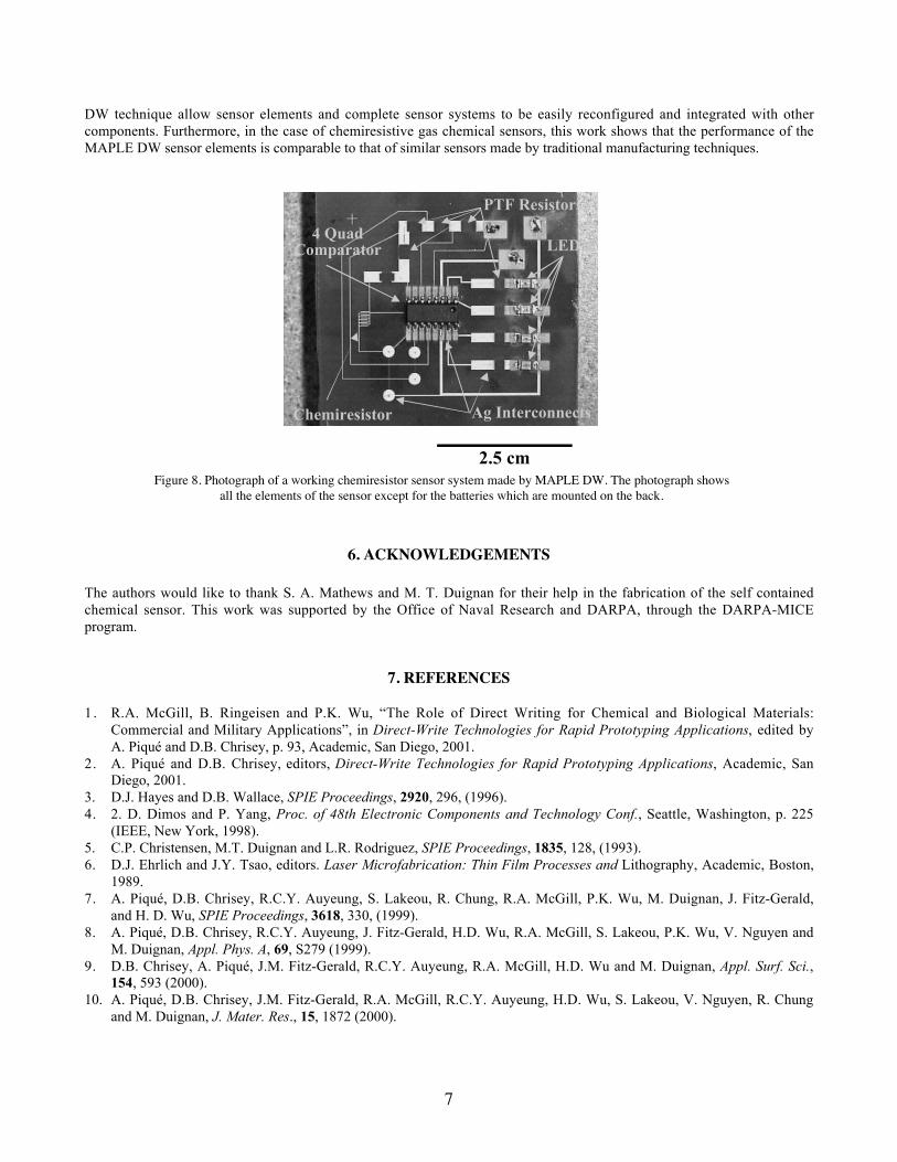
The real potential of MAPLE DW is made clear when a complete sensor system consisting of a single sensor element,interconnects and passive electronic components is fabricated using this laser direct-write technique. An actual workingexample is provided in Figure 8 which shows a photograph of a complete self contained chemical sensor systemmanufactured on a 5cm x 5 cm polyimide substrate. The majority of the components shown on this image, including thechemiresistor, the Ag interconnects and the polymer thick film resistors, but not the LED’s and the 4-quad comparator IC(which were soldered to the circuit afterwards), were fabricated by MAPLE DW. Future plans include the fabrication ofmultiple sensor elements in the form of arrays and the addition of microbatteries all made by MAPLE DW.
5. SUMMARY
MAPLE DW is an ideal process for the direct-write of sensors since it operates in air and at low temperatures. It iscompatible with many types of substrates and conditions which are ideal for the processing of numerous physical, chemicaland biological sensor materials. MAPLE DW has been used for rapid prototyping of custom-engineered physical,biological and chemical sensors in various types of geometries. The versatility and CAD/CAM features of the MAPLE
5 mm
PECH/CarbonAg Interdigitated
Electrodes
Figure 6. Optical micrograph of a chemiresistor gas sensorelement made by MAPLE DW.
0
2
4
6
8
10
12
0 2000 4000 6000 8000 10000 12000
Spray Coated PECH/CMAPLE DW PECH/C
∆R/R (%)
Time (s)
5 ppmDMMP
10 ppm
15 ppm
20 ppm
∆R
/R (
%)
0
1
2
3
4
5
0 1000 2000 3000 4000 5000 6000 7000
Spray Coated PECH/CMAPLE DW PECH/C
∆R/R (%)
Time (s)
130 ppmtoluene
260 ppm390 ppm
520 ppm
∆R
/R (
%)
(a) (b)
Figure 7. Response of a spray coated and a MAPLE DW PECH/carbon chemiresistor sensors to various concentrations of (a) tolueneand (b) DMMP vapors. The spikes on the toluene response signals are due to the syringe pump system used to generate the
calibrated vapor exposures.
7
DW technique allow sensor elements and complete sensor systems to be easily reconfigured and integrated with othercomponents. Furthermore, in the case of chemiresistive gas chemical sensors, this work shows that the performance of theMAPLE DW sensor elements is comparable to that of similar sensors made by traditional manufacturing techniques.
6. ACKNOWLEDGEMENTS
The authors would like to thank S. A. Mathews and M. T. Duignan for their help in the fabrication of the self containedchemical sensor. This work was supported by the Office of Naval Research and DARPA, through the DARPA-MICEprogram.
7. REFERENCES
1. R.A. McGill, B. Ringeisen and P.K. Wu, “The Role of Direct Writing for Chemical and Biological Materials:Commercial and Military Applications”, in Direct-Write Technologies for Rapid Prototyping Applications, edited byA. Piqué and D.B. Chrisey, p. 93, Academic, San Diego, 2001.
2. A. Piqué and D.B. Chrisey, editors, Direct-Write Technologies for Rapid Prototyping Applications, Academic, SanDiego, 2001.
3. D.J. Hayes and D.B. Wallace, SPIE Proceedings, 2920, 296, (1996).4. 2. D. Dimos and P. Yang, Proc. of 48th Electronic Components and Technology Conf., Seattle, Washington, p. 225
(IEEE, New York, 1998).5. C.P. Christensen, M.T. Duignan and L.R. Rodriguez, SPIE Proceedings, 1835, 128, (1993).6. D.J. Ehrlich and J.Y. Tsao, editors. Laser Microfabrication: Thin Film Processes and Lithography, Academic, Boston,
1989.7. A. Piqué, D.B. Chrisey, R.C.Y. Auyeung, S. Lakeou, R. Chung, R.A. McGill, P.K. Wu, M. Duignan, J. Fitz-Gerald,
and H. D. Wu, SPIE Proceedings, 3618, 330, (1999).8. A. Piqué, D.B. Chrisey, R.C.Y. Auyeung, J. Fitz-Gerald, H.D. Wu, R.A. McGill, S. Lakeou, P.K. Wu, V. Nguyen and
M. Duignan, Appl. Phys. A, 69, S279 (1999).9. D.B. Chrisey, A. Piqué, J.M. Fitz-Gerald, R.C.Y. Auyeung, R.A. McGill, H.D. Wu and M. Duignan, Appl. Surf. Sci.,
154, 593 (2000).10. A. Piqué, D.B. Chrisey, J.M. Fitz-Gerald, R.A. McGill, R.C.Y. Auyeung, H.D. Wu, S. Lakeou, V. Nguyen, R. Chung
and M. Duignan, J. Mater. Res., 15, 1872 (2000).
LED’s4 Quad
Comparator
Chemiresistor
2.5 cm
Ag Interconnects
PTF Resistors
Figure 8. Photograph of a working chemiresistor sensor system made by MAPLE DW. The photograph showsall the elements of the sensor except for the batteries which are mounted on the back.

8
11. J.M. Fitz-Gerald, A. Piqué, D.B. Chrisey, P.D. Rack, M. Zeleznik, R.C.Y. Auyeung and S. Lakeou, Appl. Phys. Lett.,76, 1386 (2000).
12. K.E. Swider-Lyons, D.W. Weir, C.T. Love, R. Modi, T. Sutto, A. Piqué and D.B. Chrisey, Power Sources for the NextMillenium, edited by M. Jain, M.A. Ryan, S. Surampdi, R.A. Marsh and G. Nagrajan, Electrochem. Soc. Proc., 2000-22, 272 (2000).
13. A. Piqué, K.E. Swider-Lyons, D.W. Weir, C.T. Love, R. Modi, SPIE Proceedings, 4274, 317, (2001).14. P.K. Wu, B. Ringeisen, J. Callahan, M. Brooks, D.M. Bubb, H.D. Wu, A. Piqué, B. Spargo, R. A. McGill and D.B.
Chrisey, Thin Solid Films, 398-399, 607 (2001).15. B. Ringeisen, D.B. Chrisey, A. Piqué, H.D. Young, R. Modi, M. Bucaro, J. Jones-Meehan and B.J. Spargo,
Biomaterials, 23, 161 (2002).16. J.W. Gardner, M. Craven, C. Dow, E.L. Hines, Meas. Sci. Technol., 9, 120 (1998).17. J.V. Hatfield, P. Neaves, P.J. Hicks, K. Persaud, P. Travers, Sens. Actuators B: Chem., 18, 221 (1994).