Embed Size (px)
Citation preview
Presented By
Dwarakaprasad Ramamoorthy
An Optimized Integrated QVCO for Use in a Clock Generator for a An Optimized Integrated QVCO for Use in a Clock Generator for a
NewNew Globally Asynchronous, Locally Synchronous (GALS) Globally Asynchronous, Locally Synchronous (GALS) Design Methodology.Design Methodology.

OverviewOverview
Background
Need for this new design methodology.
Why GALS?
What is novel in this design?
Need for QVCO
Design Strategy
Simulations & Layout
Conclusion
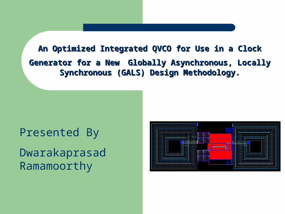
CLOCK GENERATORCLOCK GENERATOR
Clock
sin u
cos u
sin t
cos t
Phase Locked Loop
DualSample& Hold
Multiplier
Init2!
Done!
Run
CDA
Multiplier
Init1!SRFF1 SRFF2
sin tu)
Ref [1]

Simple Phase Locked LoopSimple Phase Locked Loop
Source: http://www.uoguelph.ca/~antoon/gadgets/pll/pll.html

VCO Core DesignVCO Core Design
2oscVA
SATDCnSAT VAVV 1
DCDDpSAT VAVV
Ref [4]
1
)(2
CRsLCs
RsLGsH
s
sm

SIOS (Spiral Inductor On Silicon) DesignSIOS (Spiral Inductor On Silicon) Design
Spiral Inductor Parameters
SymbolQuantity Value
D0 Outer area length 320 µm
D0 Outer area width 320 µm
W Conductor width 18 µm
S Conductor Spacing 2 µm
N Number of turns 6
Wn Return path width 18 µm
Ln Return path length 120 µm
Ls Series inductance 7.82 nH
Rs Series resistance 6.24 Ω
Q Quality factor 5
Qmax Maximum quality factor 10
fmax Frequency at Qmax 1.89 GHz
SRF Self resonating frequency 4.33 GHz
Ref [6], [8]
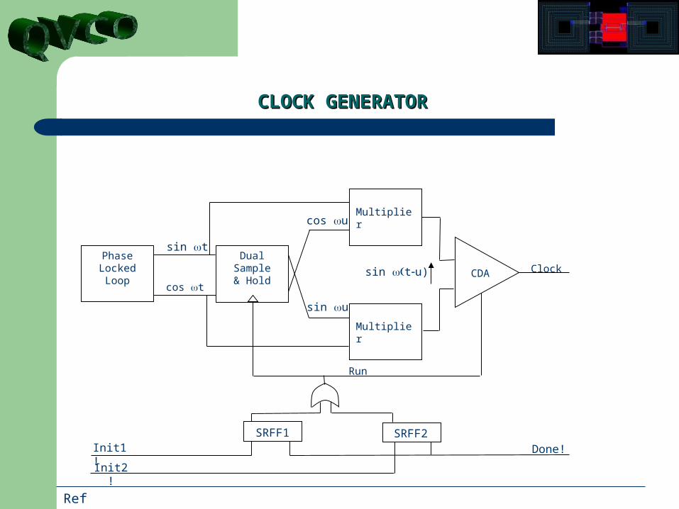
Inversion Mode (I-MOS) Varactor DesignInversion Mode (I-MOS) Varactor Design
Ref [9]

Quadrature GenerationQuadrature Generation
Ref [12], [13]

QVCO Simulation SummaryQVCO Simulation Summary

QVCO Performance SummaryQVCO Performance Summary
Center frequency 618 MHz – 687 MHz
Tuning range 10%
Phase noise -190 dBc/Hz at 600 MHz
Current consumption at 2.5 V power supply
8.4 mA
Power consumption at 2.5 V power supply
21 mW
Technology TSMC 0.25 µm, single-poly, five-metal, 2.5 V CMOS
technology

QVCO Full Custom LayoutQVCO Full Custom Layout

ConclusionConclusion
A good compromise between area and overall power consumption was achieved.
A prototype quadrature –Gm LC-VCO for 650 MHz was designed in standard 0.25 µm, single-poly,
five-metal, 2.5 V CMOS technology.
A tuning range of 10% was obtained through the use of I-MOS varactors.
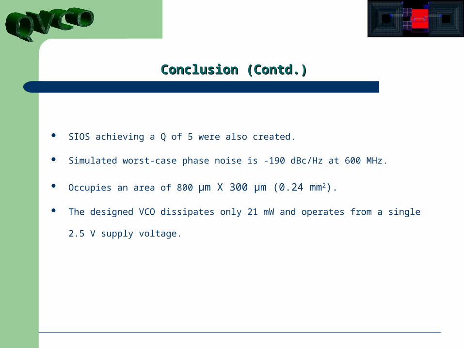
Conclusion (Contd.)Conclusion (Contd.)
SIOS achieving a Q of 5 were also created.
Simulated worst-case phase noise is -190 dBc/Hz at 600 MHz.
Occupies an area of 800 µm X 300 µm (0.24 mm2).
The designed VCO dissipates only 21 mW and operates from a single 2.5 V supply voltage.

Future WorkFuture Work
Incorporate QVCO into PLL Design.
Complete other Clock Generator Modules.

Presented By
Dwarakaprasad Ramamoorthy
An Optimized Integrated QVCO for Use in a Clock Generator for a An Optimized Integrated QVCO for Use in a Clock Generator for a New Globally Asynchronous, Locally Synchronous (GALS) Design New Globally Asynchronous, Locally Synchronous (GALS) Design
Methodology.Methodology.