Embed Size (px)
Citation preview
PRINCIPLES OF COMMUNICATION SYSTEMS LAB (EE-230-F)
DEPARTMENT OF ELECTRICAL AND ELECTRONICS ENGINEERING DRONACHARYA COLLEGE OF ENGINEERING Page 1
PRINCIPLES OF COMMUNICATION SYSTEMS
LAB
LAB MANUAL
(EE-230-F)
IV SEM ELECTRICAL AND ELECTRONICS
ENGINEERING
DEPARTMENT OF ELECTRICAL & ELECTRONICS DRONACHARYA COLLEGE OF ENGINEERING
KHENTAWAS, GURGAON-123506
PRINCIPLES OF COMMUNICATION SYSTEMS LAB (EE-230-F)
DEPARTMENT OF ELECTRICAL AND ELECTRONICS ENGINEERING DRONACHARYA COLLEGE OF ENGINEERING Page 2
CONTENTS
SUBECT: PRINCIPLES OF COMMUNICATION LAB (EE-230-F)
S.NO. Name of Experiment Page No.
1. Generation of DSB-SC AM signal using balanced modulator. 3-8 2. Generation of SSB AM signal 9-15 3. To study envelop detector for demodulation of AM signal and observe
diagonal peak clipping effect.
16-24
4. Frequency modulation using voltage controlled oscillator. 25-30 5. To generate a FM Signal using Varactor & reactance modulation.
31-37
6. Detection of FM Signal using PLL & Foster Seelay method.. 38-44 7. To Study Super heterodyne AM receiver and measurement of receiver
parameters 45-50
8.(a-c) To studyPAM/PWM & PPM modulation & demodulation. 51-59 9. Study of Frequency Division Multiplexing/Demultiplexing with
sinusoidal & audio inputs.
60-63
10. Study of 4 channel Time Division Multiplexing system. 64-68 11. Study of pulse code modulation and demodulation with parity &
Hamming code. 69-71
12.(a-b)
Study pulse data coding & decoding techniques for various formats. 72-76
13. Study of ASK, FSK modulator and demodulator. 77-81 14. Study of PSK & QPSK modulator and demodulator. 82-83
PRINCIPLES OF COMMUNICATION SYSTEMS LAB (EE-230-F)
DEPARTMENT OF ELECTRICAL AND ELECTRONICS ENGINEERING DRONACHARYA COLLEGE OF ENGINEERING Page 3
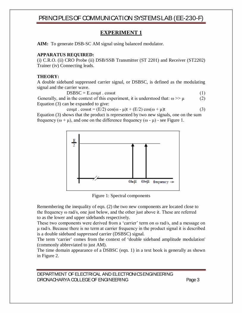
EXPERIMENT 1 AIM: To generate DSB-SC AM signal using balanced modulator. APPARATUS REQUIRED: (i) C.R.O. (ii) CRO Probe (ii) DSB/SSB Transmitter (ST 2201) and Receiver (ST2202) Trainer (iv) Connecting leads. THEORY: A double sideband suppressed carrier signal, or DSBSC, is defined as the modulating signal and the carrier wave.
DSBSC = E.cosμt . cosωt (1) Generally, and in the context of this experiment, it is understood that: ω >> μ (2) Equation (3) can be expanded to give:
cosμt . cosωt = (E/2) cos(ω - μ)t + (E/2) cos(ω + μ)t (3) Equation (3) shows that the product is represented by two new signals, one on the sum frequency (ω + μ), and one on the difference frequency (ω - μ) - see Figure 1.
Figure 1: Spectral components
Remembering the inequality of eqn. (2) the two new components are located close to the frequency ω rad/s, one just below, and the other just above it. These are referred to as the lower and upper sidebands respectively. These two components were derived from a ‘carrier’ term on ω rad/s, and a message on μ rad/s. Because there is no term at carrier frequency in the product signal it is described is a double sideband suppressed carrier (DSBSC) signal. The term ‘carrier’ comes from the context of ‘double sideband amplitude modulation' (commonly abbreviated to just AM). The time domain appearance of a DSBSC (eqn. 1) in a text book is generally as shown in Figure 2.
PRINCIPLES OF COMMUNICATION SYSTEMS LAB (EE-230-F)
DEPARTMENT OF ELECTRICAL AND ELECTRONICS ENGINEERING DRONACHARYA COLLEGE OF ENGINEERING Page 4
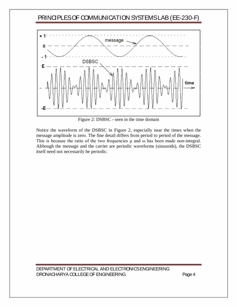
Figure 2: DSBSC - seen in the time domain
Notice the waveform of the DSBSC in Figure 2, especially near the times when the message amplitude is zero. The fine detail differs from period to period of the message. This is because the ratio of the two frequencies μ and ω has been made non-integral. Although the message and the carrier are periodic waveforms (sinusoids), the DSBSC itself need not necessarily be periodic.
PRINCIPLES OF COMMUNICATION SYSTEMS LAB (EE-230-F)
DEPARTMENT OF ELECTRICAL AND ELECTRONICS ENGINEERING DRONACHARYA COLLEGE OF ENGINEERING Page 5
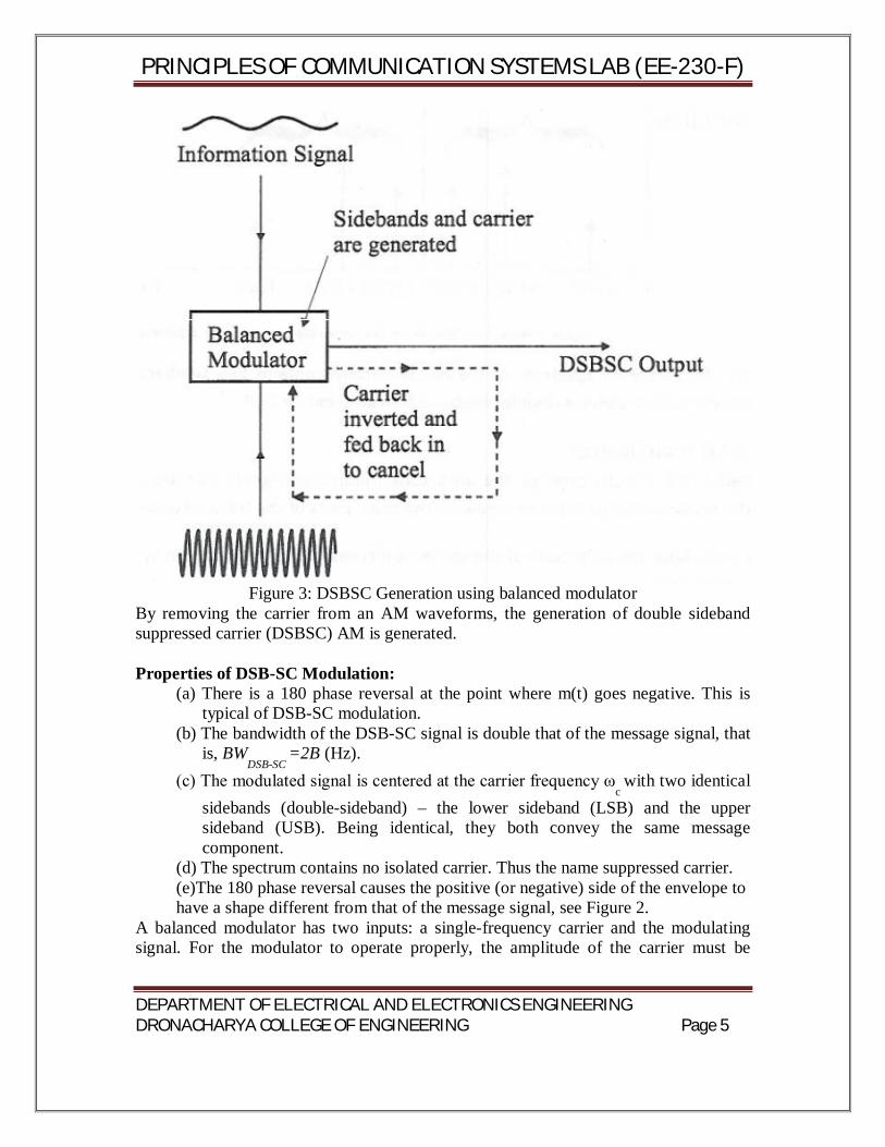
Figure 3: DSBSC Generation using balanced modulator
By removing the carrier from an AM waveforms, the generation of double sideband suppressed carrier (DSBSC) AM is generated. Properties of DSB-SC Modulation:
(a) There is a 180 phase reversal at the point where m(t) goes negative. This is typical of DSB-SC modulation.
(b) The bandwidth of the DSB-SC signal is double that of the message signal, that is, BW
DSB-SC =2B (Hz).
(c) The modulated signal is centered at the carrier frequency ωc with two identical
sidebands (double-sideband) – the lower sideband (LSB) and the upper sideband (USB). Being identical, they both convey the same message component.
(d) The spectrum contains no isolated carrier. Thus the name suppressed carrier. (e)The 180 phase reversal causes the positive (or negative) side of the envelope to have a shape different from that of the message signal, see Figure 2.
A balanced modulator has two inputs: a single-frequency carrier and the modulating signal. For the modulator to operate properly, the amplitude of the carrier must be
PRINCIPLES OF COMMUNICATION SYSTEMS LAB (EE-230-F)
DEPARTMENT OF ELECTRICAL AND ELECTRONICS ENGINEERING DRONACHARYA COLLEGE OF ENGINEERING Page 6
sufficiently greater than the amplitude of the modulating signal (approximately six to seven times greater). PROCEDURE 1. Ensure that the following initial conditions exist on the board.
a. Audio input select switch in INT position: b. Mode switches in DSB position. c. Output amplifier's gain pot in full clockwise position. d. Speakers switch in OFF position.
2. Turn on power to the ST2201 board. 3. Turn the audio oscillator block's amplitude pot to its full clockwise (MAX) position, and examine the block's output (t.p.14) on an oscilloscope. This is the audio frequency sine wave which will be our modulating signal. Note that the sine wave’s frequency can be adjusted from about 300 Hz to approximately 3.4 KHz, by adjusting the audio oscillator's frequency potmeter. Note also that the amplitude of this audio modulating signal can be reduced to zero, by turning the Audio oscillator's amplitude potmeter to its fully counterclockwise (MIN) position. Return the amplitude present to its max position. 4. Turn the balance pot, in the balanced modulator & band pass filter circuit 1 block, to its fully clockwise position. It is this block that we will use to perform double-side band amplitude modulation. 5. Monitor, in turn, the two inputs to the balanced modulator & band pass filter circuits block, at t.p.1 and t.p.9. Note that:
a. The signal at t.p.1 is the audio-frequency sine wave from the audio oscillator block. This is the modulating input to our double-sideband modulator. b. Test point 9 carries a sine wave of 1MHz frequency and amplitude 120mVpp approx. This is the carrier input to our double-sideband modulator.
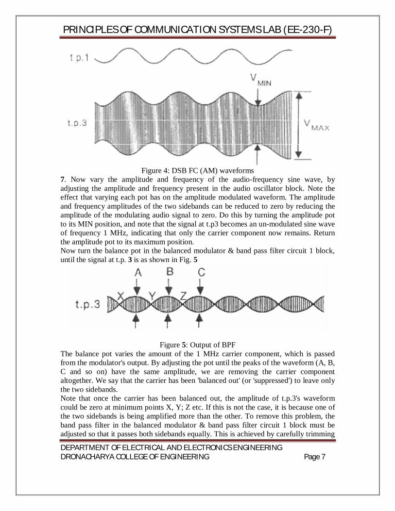
6. Next, examine the output of the balanced modulator & band pass filter circuit 1 block (at t.p.3), together with the modulating signal at t.p.1 Trigger the oscilloscope on the t.p. 1 signal. The output from the balanced modulator & band pass filter circuit 1 block (at t.p. 3) is a DSBFC AM waveform, which has been formed by amplitude-modulating the 1MHz carrier sine wave with the audio-frequency sine wave from the audio oscillator.
PRINCIPLES OF COMMUNICATION SYSTEMS LAB (EE-230-F)
DEPARTMENT OF ELECTRICAL AND ELECTRONICS ENGINEERING DRONACHARYA COLLEGE OF ENGINEERING Page 7
Figure 4: DSB FC (AM) waveforms
7. Now vary the amplitude and frequency of the audio-frequency sine wave, by adjusting the amplitude and frequency present in the audio oscillator block. Note the effect that varying each pot has on the amplitude modulated waveform. The amplitude and frequency amplitudes of the two sidebands can be reduced to zero by reducing the amplitude of the modulating audio signal to zero. Do this by turning the amplitude pot to its MIN position, and note that the signal at t.p3 becomes an un-modulated sine wave of frequency 1 MHz, indicating that only the carrier component now remains. Return the amplitude pot to its maximum position. Now turn the balance pot in the balanced modulator & band pass filter circuit 1 block, until the signal at t.p. 3 is as shown in Fig. 5
Figure 5: Output of BPF
The balance pot varies the amount of the 1 MHz carrier component, which is passed from the modulator's output. By adjusting the pot until the peaks of the waveform (A, B, C and so on) have the same amplitude, we are removing the carrier component altogether. We say that the carrier has been 'balanced out' (or 'suppressed') to leave only the two sidebands. Note that once the carrier has been balanced out, the amplitude of t.p.3's waveform could be zero at minimum points X, Y; Z etc. If this is not the case, it is because one of the two sidebands is being amplified more than the other. To remove this problem, the band pass filter in the balanced modulator & band pass filter circuit 1 block must be adjusted so that it passes both sidebands equally. This is achieved by carefully trimming
PRINCIPLES OF COMMUNICATION SYSTEMS LAB (EE-230-F)
DEPARTMENT OF ELECTRICAL AND ELECTRONICS ENGINEERING DRONACHARYA COLLEGE OF ENGINEERING Page 8
transformer T1, until the waveform's amplitude is as close to zero as possible at the minimum points. The waveform at t.p.3 is known as a double-side suppressed carrier (DSBSC) waveform, and its frequency spectrum is as shown in Fig.1. Note that now only the two sidebands remain, the carrier component has been removed. 8. Change the amplitude and frequency of the modulating audio signal (by adjusting the audio oscillator block's amplitude and frequency pots), and note the effect that these changes on the DSBSC waveform. The amplitudes of the two sidebands can be reduced to zero by reducing the amplitude of the modulating audio signal to zero. Do these by turning the amplitude present to its MIN position, and note that the monitored signal becomes a D C level, indicating that there .are now no frequency components present. Return the amplitude pot to its MAX position. 9. Examine the output from the output amplifier block (t.p.13), together with the audio modulating signal (at t.p.1), triggering the scope with the audio modulating signal. Note that the DSBSC waveform appears, amplified slightly at t.p.13, as we will see later, it is the output amplifier's output signal which will be transmitted to the receiver. 10. By using the microphone, the human voice can be used as the modulating signal, instead of using ST2201's audio oscillator block. Connect the module's output to the external audio input on the ST2201 board, and put the audio input select switch in the ext position. The input signal to the audio input module may be taken from an external microphone or from a cassette recorder, by choosing the appropriate switch setting on the module. RESULTs:- The DSBSC signal has been generated using balanced modulator. WAVE FORMS OBSERVED:- Draw wave forms as observed on CRO and label the different waveforms appropriately. PRECAUTIONS:- 1. Do not use open ended wires for connecting to 230 V power supply. 2. Before connecting the power supply plug into socket, ensure power supply should be switched off 3. Ensure all connections should be tight before switching on the power supply. 4. Take the reading carefully. 5. Power supply should be switched off after completion of experiment. QUIZ / ANSWERS:- Q. 1. What is modulation? Ans. Modulation is a process in which the amplitude of the carrier is made proportional to the instantaneous amplitude of the modulating signal. Q. 2. Which are the three discrete frequencies in AM? Ans. (1) Carrier frequency (2) lower sideband frequency (3) upper sideband frequency Q. 3 How many sidebands in AM?
PRINCIPLES OF COMMUNICATION SYSTEMS LAB (EE-230-F)
DEPARTMENT OF ELECTRICAL AND ELECTRONICS ENGINEERING DRONACHARYA COLLEGE OF ENGINEERING Page 9
Ans. There are two sidebands in AM i.e. LSB and USB Q. 4. Which are the two methods of AM generation? Ans. (1) single sideband (2) double sideband Q. 6. Write the methods of DSBSC generation. Ans. (1) Balanced Modulator (2) Ring Modulator (3) Switching Modulator Q. 7. What is the unit of modulation index in AM? Ans. It is unit less. Q. 8. Where the modulation index lies? Ans. modulation index always lies between 0 and 1. More than 1 is over modulation. Q. 9. What happens in case of over modulation? Ans. The wave will get distorted. Q. 10. Audio frequency range lies between. Ans. 20 Hz to 20 KHz.
PRINCIPLES OF COMMUNICATION SYSTEMS LAB (EE-230-F)
DEPARTMENT OF ELECTRICAL AND ELECTRONICS ENGINEERING DRONACHARYA COLLEGE OF ENGINEERING Page 10
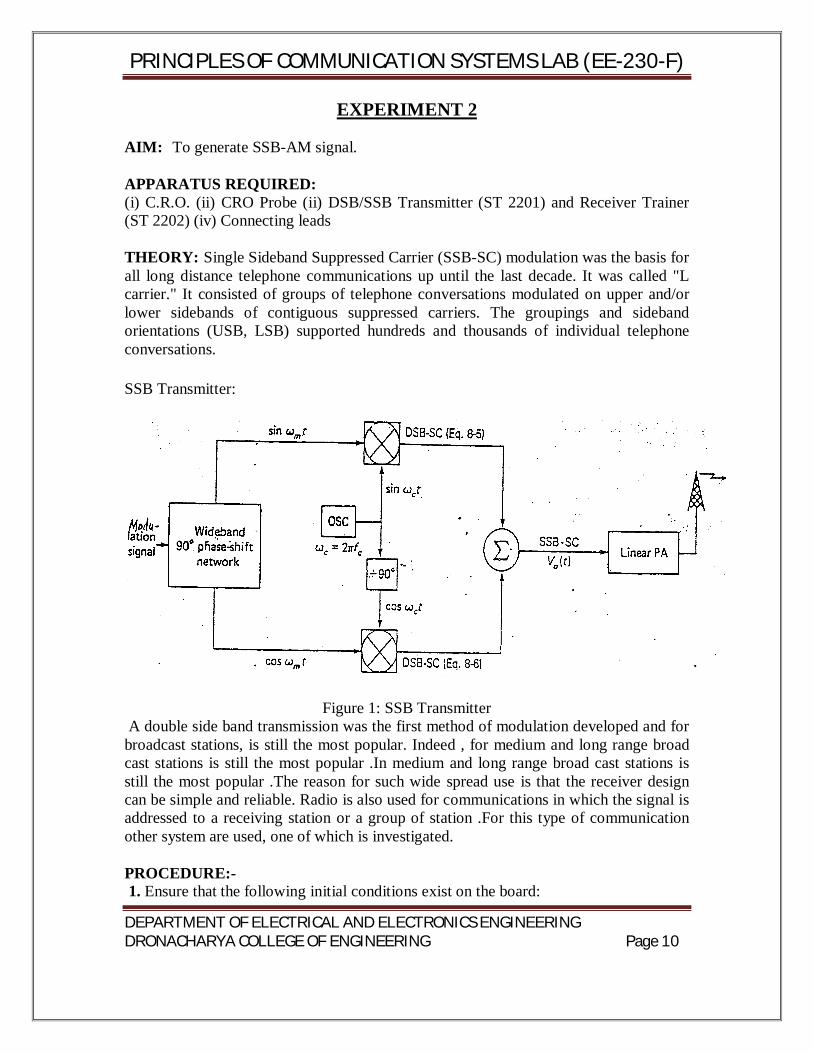
EXPERIMENT 2 AIM: To generate SSB-AM signal. APPARATUS REQUIRED: (i) C.R.O. (ii) CRO Probe (ii) DSB/SSB Transmitter (ST 2201) and Receiver Trainer (ST 2202) (iv) Connecting leads THEORY: Single Sideband Suppressed Carrier (SSB-SC) modulation was the basis for all long distance telephone communications up until the last decade. It was called "L carrier." It consisted of groups of telephone conversations modulated on upper and/or lower sidebands of contiguous suppressed carriers. The groupings and sideband orientations (USB, LSB) supported hundreds and thousands of individual telephone conversations. SSB Transmitter:
Figure 1: SSB Transmitter A double side band transmission was the first method of modulation developed and for broadcast stations, is still the most popular. Indeed , for medium and long range broad cast stations is still the most popular .In medium and long range broad cast stations is still the most popular .The reason for such wide spread use is that the receiver design can be simple and reliable. Radio is also used for communications in which the signal is addressed to a receiving station or a group of station .For this type of communication other system are used, one of which is investigated. PROCEDURE:- 1. Ensure that the following initial conditions exist on the board:
PRINCIPLES OF COMMUNICATION SYSTEMS LAB (EE-230-F)
DEPARTMENT OF ELECTRICAL AND ELECTRONICS ENGINEERING DRONACHARYA COLLEGE OF ENGINEERING Page 11
a) Audio input select switch in INT position. b) Mode switch in SSB position. c) Output amplifier's gain pot in fully clockwise position. d) Speaker switch in OFF position.
2. Turn on power to the ST2201 board. 3. Turn the audio oscillator block's amplitude pot to its fully clockwise (MAX) position, and examine the block's output (t.p.14) on an oscilloscope. This is the audio frequency sine wave which will be used as out modulating signal. Note that the sine wave’s frequency can be adjusted from about 300Hz to approximately 3.4 KHz, by adjusting the audio oscillator's frequency pot. Note: That the amplitude of this audio modulating signal can be reduced to zero, by turning the audio oscillator's pot to its fully counter-clockwise (MIN) position. Leave the amplitude pot on its full clockwise position, and adjust the frequency pot for an audio frequency of 2 KHz, approx. (mid-way). 4. To achieve signal- sideband amplitude modulation, we will utilize the following three blocks on the ST2201 module.
a) Balanced modulator. b) Ceramic band pass filter c) Balanced modulator & band pass filter circuit 2.
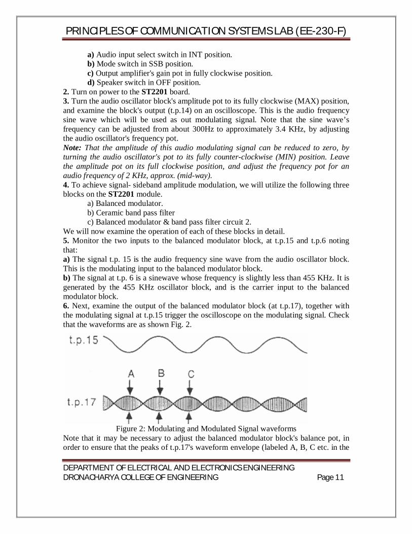
We will now examine the operation of each of these blocks in detail. 5. Monitor the two inputs to the balanced modulator block, at t.p.15 and t.p.6 noting that: a) The signal t.p. 15 is the audio frequency sine wave from the audio oscillator block. This is the modulating input to the balanced modulator block. b) The signal at t.p. 6 is a sinewave whose frequency is slightly less than 455 KHz. It is generated by the 455 KHz oscillator block, and is the carrier input to the balanced modulator block. 6. Next, examine the output of the balanced modulator block (at t.p.17), together with the modulating signal at t.p.15 trigger the oscilloscope on the modulating signal. Check that the waveforms are as shown Fig. 2.
Figure 2: Modulating and Modulated Signal waveforms
Note that it may be necessary to adjust the balanced modulator block's balance pot, in order to ensure that the peaks of t.p.17's waveform envelope (labeled A, B, C etc. in the
PRINCIPLES OF COMMUNICATION SYSTEMS LAB (EE-230-F)
DEPARTMENT OF ELECTRICAL AND ELECTRONICS ENGINEERING DRONACHARYA COLLEGE OF ENGINEERING Page 12
above diagram) all have equal amplitude. You will recall that the waveform at t.p.17 was encountered in the previous experiment this is a double-sideband suppressed carrier (DSBSC) AM waveform, and it has been obtained by amplitude-modulating the carrier sine wave at t.p. 6 of frequency fc with the audio-frequency modulating signal at t.p. 15 of frequency fm, and then removing the carrier component from the resulting AM signal, by adjusting the balance pot. The frequency spectrum of this DSBSC waveform is shown in Fig.3.
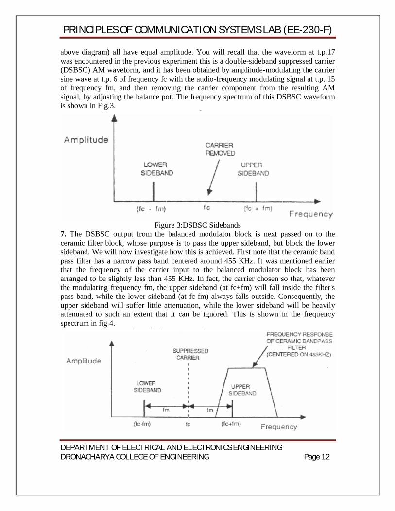
Figure 3:DSBSC Sidebands
7. The DSBSC output from the balanced modulator block is next passed on to the ceramic filter block, whose purpose is to pass the upper sideband, but block the lower sideband. We will now investigate how this is achieved. First note that the ceramic band pass filter has a narrow pass band centered around 455 KHz. It was mentioned earlier that the frequency of the carrier input to the balanced modulator block has been arranged to be slightly less than 455 KHz. In fact, the carrier chosen so that, whatever the modulating frequency fm, the upper sideband (at fc+fm) will fall inside the filter's pass band, while the lower sideband (at fc-fm) always falls outside. Consequently, the upper sideband will suffer little attenuation, while the lower sideband will be heavily attenuated to such an extent that it can be ignored. This is shown in the frequency spectrum in fig 4.
PRINCIPLES OF COMMUNICATION SYSTEMS LAB (EE-230-F)
DEPARTMENT OF ELECTRICAL AND ELECTRONICS ENGINEERING DRONACHARYA COLLEGE OF ENGINEERING Page 13
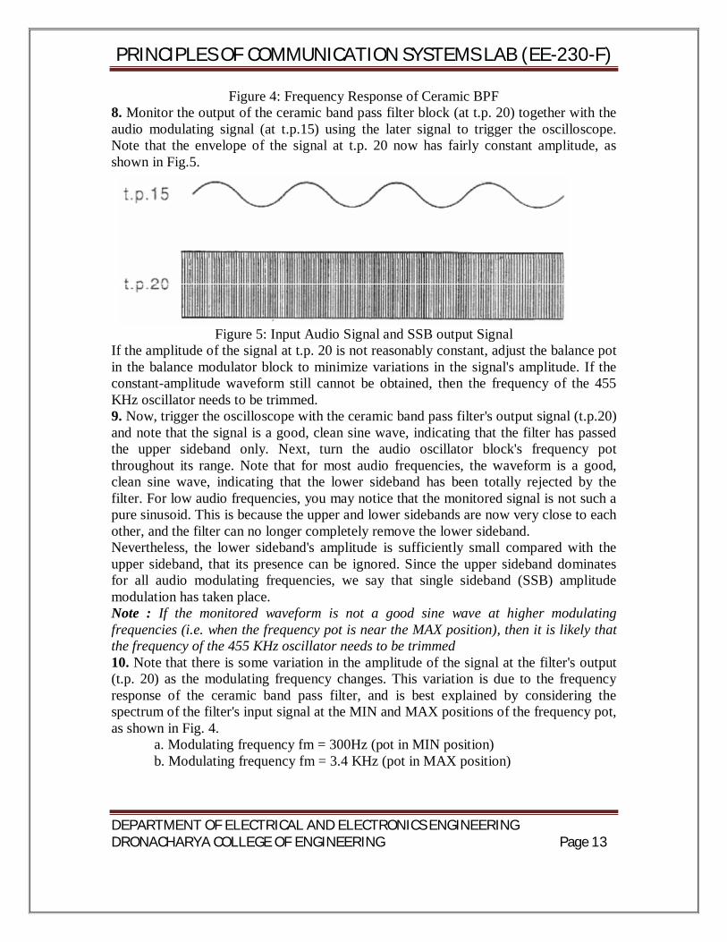
Figure 4: Frequency Response of Ceramic BPF 8. Monitor the output of the ceramic band pass filter block (at t.p. 20) together with the audio modulating signal (at t.p.15) using the later signal to trigger the oscilloscope. Note that the envelope of the signal at t.p. 20 now has fairly constant amplitude, as shown in Fig.5.
Figure 5: Input Audio Signal and SSB output Signal If the amplitude of the signal at t.p. 20 is not reasonably constant, adjust the balance pot in the balance modulator block to minimize variations in the signal's amplitude. If the constant-amplitude waveform still cannot be obtained, then the frequency of the 455 KHz oscillator needs to be trimmed. 9. Now, trigger the oscilloscope with the ceramic band pass filter's output signal (t.p.20) and note that the signal is a good, clean sine wave, indicating that the filter has passed the upper sideband only. Next, turn the audio oscillator block's frequency pot throughout its range. Note that for most audio frequencies, the waveform is a good, clean sine wave, indicating that the lower sideband has been totally rejected by the filter. For low audio frequencies, you may notice that the monitored signal is not such a pure sinusoid. This is because the upper and lower sidebands are now very close to each other, and the filter can no longer completely remove the lower sideband. Nevertheless, the lower sideband's amplitude is sufficiently small compared with the upper sideband, that its presence can be ignored. Since the upper sideband dominates for all audio modulating frequencies, we say that single sideband (SSB) amplitude modulation has taken place. Note : If the monitored waveform is not a good sine wave at higher modulating frequencies (i.e. when the frequency pot is near the MAX position), then it is likely that the frequency of the 455 KHz oscillator needs to be trimmed 10. Note that there is some variation in the amplitude of the signal at the filter's output (t.p. 20) as the modulating frequency changes. This variation is due to the frequency response of the ceramic band pass filter, and is best explained by considering the spectrum of the filter's input signal at the MIN and MAX positions of the frequency pot, as shown in Fig. 4.
a. Modulating frequency fm = 300Hz (pot in MIN position) b. Modulating frequency fm = 3.4 KHz (pot in MAX position)
PRINCIPLES OF COMMUNICATION SYSTEMS LAB (EE-230-F)
DEPARTMENT OF ELECTRICAL AND ELECTRONICS ENGINEERING DRONACHARYA COLLEGE OF ENGINEERING Page 14
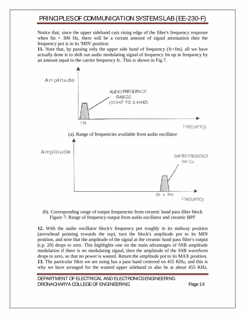
Notice that, since the upper sideband cuts rising edge of the filter's frequency response when fm = 300 Hz, there will be a certain amount of signal attenuation then the frequency pot is in its 'MIN' position. 11. Note that, by passing only the upper side band of frequency (fc+fm), all we have actually done is to shift out audio modulating signal of frequency fm up in frequency by an amount equal to the carrier frequency fc. This is shown in Fig.7.
(a). Range of frequencies available from audio oscillator
(b). Corresponding range of output frequencies from ceramic band pass filter block Figure 7: Range of frequency output from audio oscillator and ceramic BPF
12. With the audio oscillator block's frequency pot roughly in its midway position (arrowhead pointing towards the top), turn the block's amplitude pot to its MIN position, and note that the amplitude of the signal at the ceramic band pass filter's output (t.p. 20) drops to zero. This highlights one on the main advantages of SSB amplitude modulation if there is no modulating signal, then the amplitude of the SSB waveform drops to zero, so that no power is wasted. Return the amplitude pot to its MAX position. 13. The particular filter we are using has a pass band centered on 455 KHz, and this is why we have arranged for the wanted upper sideband to also be at about 455 KHz.
PRINCIPLES OF COMMUNICATION SYSTEMS LAB (EE-230-F)
DEPARTMENT OF ELECTRICAL AND ELECTRONICS ENGINEERING DRONACHARYA COLLEGE OF ENGINEERING Page 15
However, there is a disadvantage of this type of filter is the range of frequencies that the filter will pass is fixed during the filter's manufacture, and cannot subsequently be altered. Note that since there is a large gap between the upper and lower sidebands (a gap of about 910 KHz), a band pass filter with a very sharp response is not needed to reject the lower sideband, a simple tuned circuit band pass filter is quite sufficient. 14. Now examine the output of the balanced modulator & band pass filter circuit 2 block (t.p.22), and check that the waveform is a good sine wave of frequency approximately 1.45MHz. This indicates that only the upper sideband is being passed by the block. Check that the waveform is reasonably good sinusoid for all audio modulating frequencies (i.e. all positions of the audio oscillator’s frequency pot). If this is not the case, it may be that the balance pot (in the balanced modulator & band pass filter circuit 2 blocks) needs adjusting, to remove any residual carrier component at 1 MHz. If a reasonably clean sine wave still cannot be obtained for all audio frequencies, then the response of the tuned circuit band pass filter needs adjusting. This is achieved by adjusting transformer T4 in the balanced modulator & band-pass filter circuit 2 block When the modulating audio signal is swept over its entire range (a range of 3.4 KHz – 300 Hz = 3.1 KHz), the SSB waveform at t.p. 22 sweeps over the same frequency range. So single-sideband modulation has simply served to shift our range of audio frequencies up so they are centered on 1.455 MHz. 15. Monitor the 1.455 MHz SSB signal (at t.p. 22) together with the audio modulating signal (t.p. 15), triggering the scope with the later. Reduce the amplitude of the audio modulating signal to zero (by means of the audio oscillator block's amplitude pot), and note that the amplitude of the SSB signal also drops to zero, as expected. Return the amplitude pot to its MAX position. 16. Examine the final SSB output (at t.p. 22) together with the output from the output amplifier block (t.p. 13). Note that the final SSB waveform appears, amplified slightly, at t.p. 13. As we still see later, it is the output signal which will be transmitted to the receiver. 17. By using the microphone the human voice can be used as the audio modulating signal, instead of using ST2201's audio oscillator block. Connect the microphone to the external audio input on the ST2201 board, and put the audio input select switch in the EXT position. The input signal to the audio input select may be taken from an external microphone (supplied with the module) of from a cassette recorder, by choosing the appropriate switch setting on the module. RESULTs:- The SSB signal has been generated using balanced modulator. PRECAUTIONS:- 1. Do not use open ended wires for connecting to 230 V power supply. 2. Before connecting the power supply plug into socket, ensure power supply should be switched off
PRINCIPLES OF COMMUNICATION SYSTEMS LAB (EE-230-F)
DEPARTMENT OF ELECTRICAL AND ELECTRONICS ENGINEERING DRONACHARYA COLLEGE OF ENGINEERING Page 16
3. Ensure all connections should be tight before switching on the power supply. 4. Take the reading carefully. 5. Power supply should be switched off after completion of experiment QUIZ / ANSWERS:- Q.1. What is the most commonly used demodulator? Ans. Diode detector. Q.2. What is AGC? Ans. AGC stands for automatic gain control. Q.3. What is the use of AGC? Ans. AGC circuit is used to prevent overloading receiver and also reduce the effect of fluctuations in the received signal strength. Q.4. What is the required oscillator frequency in AM receiver? Ans. The required oscillator frequency in AM receiver is always higher than the signal frequency. Q.5. What is the use of pilot carrier in SSB? Ans. For frequency stabilization. Q.6. Which circuit is not be used to demodulate SSB? Ans. Phase discriminator. Q.7. What is the advantage of SSB over DSB? Ans. Transmitter circuit is more stable, giving batter reception. Q.8.Which type of modulation is used in India for video transmission? Ans. Amplitude Modulation. Q.9. Which filter is used in SSB generation? Ans. Mechanical filters. Q.10. How AM signals with large carrier are detected? Ans. By using envelope detector
PRINCIPLES OF COMMUNICATION SYSTEMS LAB (EE-230-F)
DEPARTMENT OF ELECTRICAL AND ELECTRONICS ENGINEERING DRONACHARYA COLLEGE OF ENGINEERING Page 17
EXPERIMENT 3
AIM: To study envelope detector for AM signal and observe peak diagonal clipping
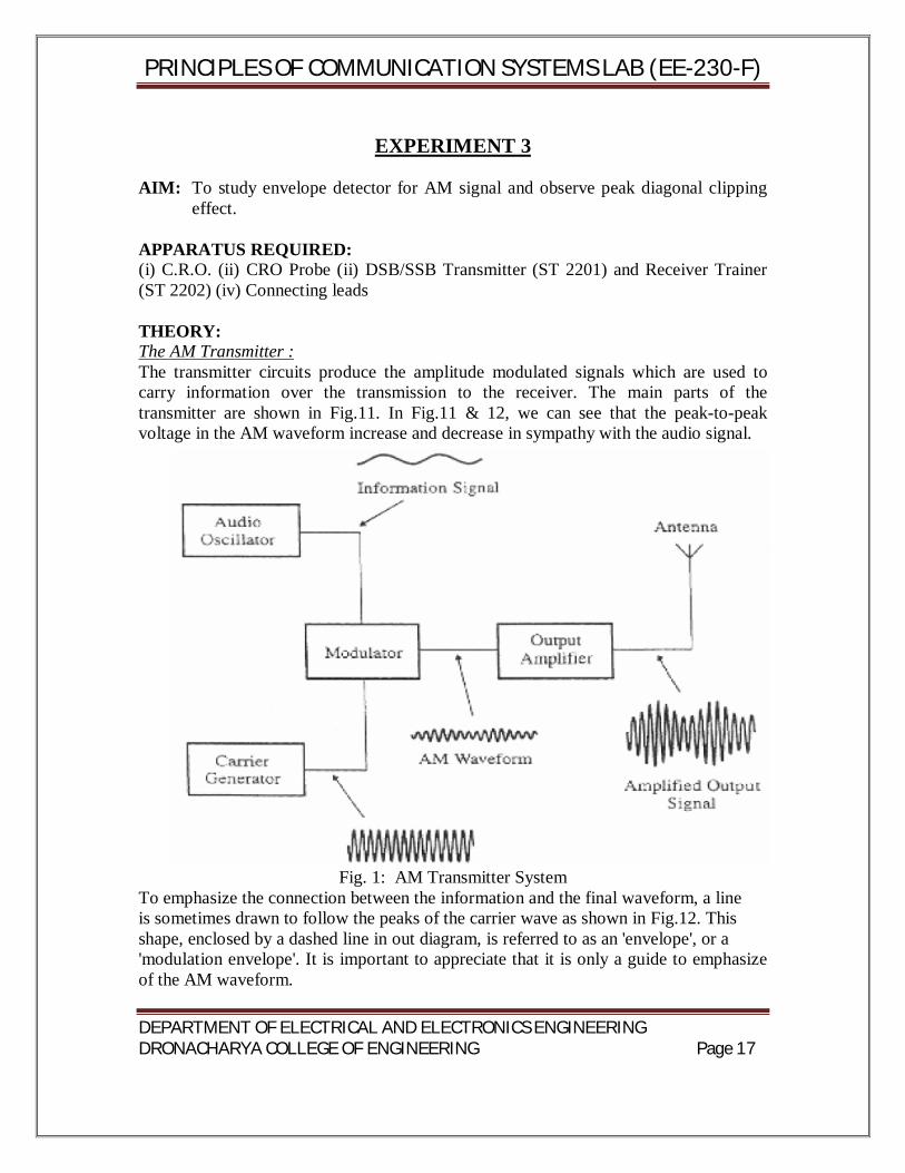
effect. APPARATUS REQUIRED: (i) C.R.O. (ii) CRO Probe (ii) DSB/SSB Transmitter (ST 2201) and Receiver Trainer (ST 2202) (iv) Connecting leads THEORY: The AM Transmitter : The transmitter circuits produce the amplitude modulated signals which are used to carry information over the transmission to the receiver. The main parts of the transmitter are shown in Fig.11. In Fig.11 & 12, we can see that the peak-to-peak voltage in the AM waveform increase and decrease in sympathy with the audio signal.
Fig. 1: AM Transmitter System
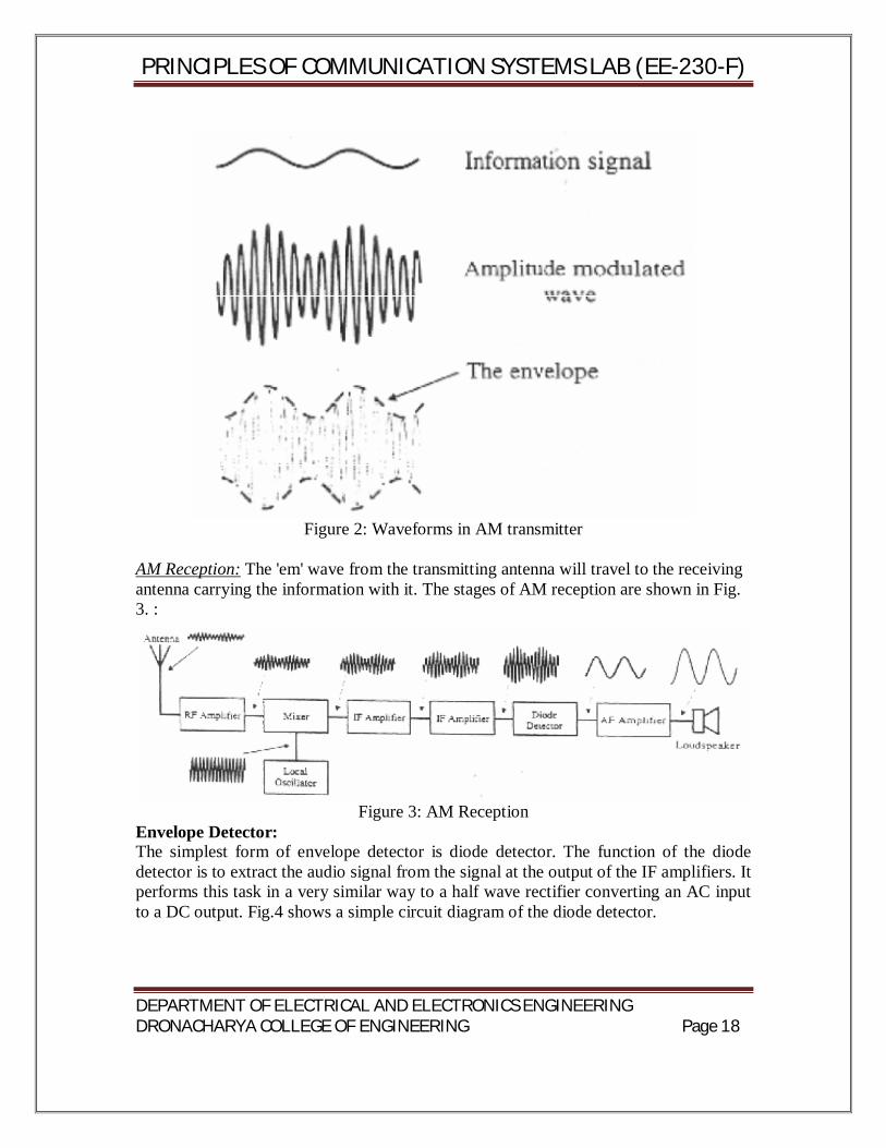
To emphasize the connection between the information and the final waveform, a line is sometimes drawn to follow the peaks of the carrier wave as shown in Fig.12. This shape, enclosed by a dashed line in out diagram, is referred to as an 'envelope', or a 'modulation envelope'. It is important to appreciate that it is only a guide to emphasize of the AM waveform.
PRINCIPLES OF COMMUNICATION SYSTEMS LAB (EE-230-F)
DEPARTMENT OF ELECTRICAL AND ELECTRONICS ENGINEERING DRONACHARYA COLLEGE OF ENGINEERING Page 18
Figure 2: Waveforms in AM transmitter
AM Reception: The 'em' wave from the transmitting antenna will travel to the receiving antenna carrying the information with it. The stages of AM reception are shown in Fig. 3. :
Figure 3: AM Reception
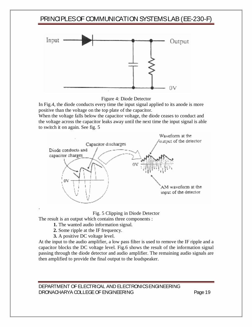
Envelope Detector: The simplest form of envelope detector is diode detector. The function of the diode detector is to extract the audio signal from the signal at the output of the IF amplifiers. It performs this task in a very similar way to a half wave rectifier converting an AC input to a DC output. Fig.4 shows a simple circuit diagram of the diode detector.
PRINCIPLES OF COMMUNICATION SYSTEMS LAB (EE-230-F)
DEPARTMENT OF ELECTRICAL AND ELECTRONICS ENGINEERING DRONACHARYA COLLEGE OF ENGINEERING Page 19
Figure 4: Diode Detector
In Fig.4, the diode conducts every time the input signal applied to its anode is more positive than the voltage on the top plate of the capacitor. When the voltage falls below the capacitor voltage, the diode ceases to conduct and the voltage across the capacitor leaks away until the next time the input signal is able to switch it on again. See fig. 5
. Fig. 5 Clipping in Diode Detector
The result is an output which contains three components : 1. The wanted audio information signal. 2. Some ripple at the IF frequency. 3. A positive DC voltage level.
At the input to the audio amplifier, a low pass filter is used to remove the IF ripple and a capacitor blocks the DC voltage level. Fig.6 shows the result of the information signal passing through the diode detector and audio amplifier. The remaining audio signals are then amplified to provide the final output to the loudspeaker.
PRINCIPLES OF COMMUNICATION SYSTEMS LAB (EE-230-F)
DEPARTMENT OF ELECTRICAL AND ELECTRONICS ENGINEERING DRONACHARYA COLLEGE OF ENGINEERING Page 20
Figure 6: Output of Diode Detector and output Filter
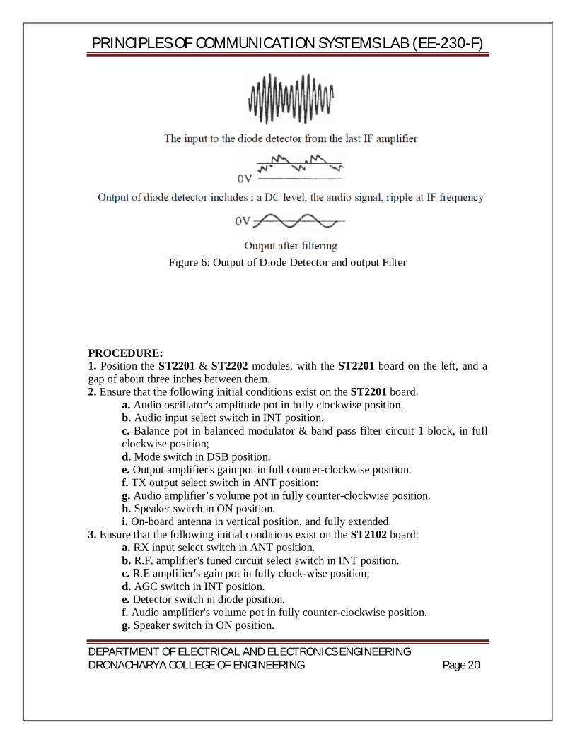
PROCEDURE: 1. Position the ST2201 & ST2202 modules, with the ST2201 board on the left, and a gap of about three inches between them. 2. Ensure that the following initial conditions exist on the ST2201 board.
a. Audio oscillator's amplitude pot in fully clockwise position. b. Audio input select switch in INT position. c. Balance pot in balanced modulator & band pass filter circuit 1 block, in full clockwise position; d. Mode switch in DSB position. e. Output amplifier's gain pot in full counter-clockwise position. f. TX output select switch in ANT position: g. Audio amplifier’s volume pot in fully counter-clockwise position. h. Speaker switch in ON position. i. On-board antenna in vertical position, and fully extended.
3. Ensure that the following initial conditions exist on the ST2102 board: a. RX input select switch in ANT position. b. R.F. amplifier's tuned circuit select switch in INT position. c. R.E amplifier's gain pot in fully clock-wise position; d. AGC switch in INT position. e. Detector switch in diode position. f. Audio amplifier's volume pot in fully counter-clockwise position. g. Speaker switch in ON position.
PRINCIPLES OF COMMUNICATION SYSTEMS LAB (EE-230-F)
DEPARTMENT OF ELECTRICAL AND ELECTRONICS ENGINEERING DRONACHARYA COLLEGE OF ENGINEERING Page 21
h. Beat frequency oscillator switch in OFF position. i. On-board antenna in vertical position, and fully extended.
4. Turn on power to the modules. 5. On the ST2202 module, slowly turn the audio amplifier's volume pot clockwise, until sounds can be heard from the on-board loudspeaker. Next, turn the vernier tuning dial until a broad cast station can be heard clearly, and adjust the volume control to a comfortable level. Note: If desired, headphones (supplied with the module) may be used instead of the on-board loudspeaker. To use the headphones, simply plug the headphone jack into the audio amplifier block's headphones socket, and adjust controlled block's volume pot. 6. The first stage or 'front end' of the ST2202 AM receiver is the R.F amplifier stage. This is a wide -bandwidth tuned amplifier stage, which is tuned into the wanted station by means of the tuning dial. Once it has been tuned into the wanted station, the R.F. amplifier, having little selectivity, will not only amplify, but also those frequencies that are close to the wanted frequency. As we will see later, these nearby frequencies will be removed by subsequent stages of the receiver, to leave only the wanted signal. Examine the envelope of the signal at the R.F. amplifier's output (at t.p. 12), with an a.c. - coupled oscilloscope channel. Note that:
a. The amplifier's output signal is very small in amplitude (a few tens of millivolts at the most). This is because one stage of amplification is not sufficient to bring the signal's amplitude up to a reasonable level. b. Only a very small amount of amplitude modulation can be detected, if any.
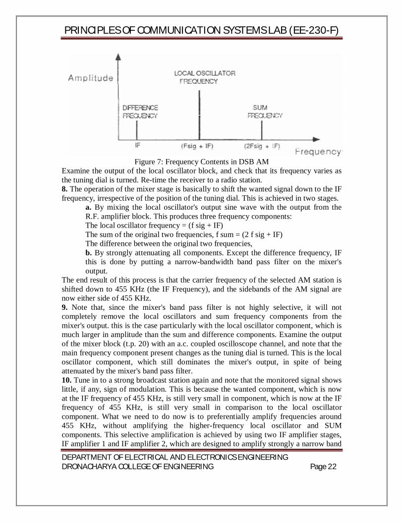
This is because there are many unwanted frequencies getting through to the amplifier output, which tend to 'drown out' the wanted AM Signal. You may notice that the waveform itself drifts up and down on the scope display, indicating that the waveform's average level is changing. This is due to the operation of the AGC circuit, which will be explained later. 7. The next stage of the receiver is the mixer stage, which mixes the R.F. amplifier's output with the output of a local oscillator. The Frequency of the local oscillator is also tuned by means of the tuning dial, and is arranged so that its frequency is always 455 KHz above the signal frequency that the R.F. amplifier is tuned to. This fixed frequency difference is always present, irrespective of the position of the tuning dial, and is arranged so that its frequency is always 455 KHz above the signal frequency that the R.F. amplifier is tuned to. This fixed frequency difference is always present, irrespective of the position of the tuning dial, and is known as the intermediate frequency (IF for short). This frequency relationship is shown below, for some arbitrary position of the tuning dial.
PRINCIPLES OF COMMUNICATION SYSTEMS LAB (EE-230-F)
DEPARTMENT OF ELECTRICAL AND ELECTRONICS ENGINEERING DRONACHARYA COLLEGE OF ENGINEERING Page 22
Figure 7: Frequency Contents in DSB AM
Examine the output of the local oscillator block, and check that its frequency varies as the tuning dial is turned. Re-time the receiver to a radio station. 8. The operation of the mixer stage is basically to shift the wanted signal down to the IF frequency, irrespective of the position of the tuning dial. This is achieved in two stages.
a. By mixing the local oscillator's output sine wave with the output from the R.F. amplifier block. This produces three frequency components: The local oscillator frequency = (f sig + IF) The sum of the original two frequencies, f sum = (2 f sig + IF) The difference between the original two frequencies, b. By strongly attenuating all components. Except the difference frequency, IF this is done by putting a narrow-bandwidth band pass filter on the mixer's output.
The end result of this process is that the carrier frequency of the selected AM station is shifted down to 455 KHz (the IF Frequency), and the sidebands of the AM signal are now either side of 455 KHz. 9. Note that, since the mixer's band pass filter is not highly selective, it will not completely remove the local oscillators and sum frequency components from the mixer's output. this is the case particularly with the local oscillator component, which is much larger in amplitude than the sum and difference components. Examine the output of the mixer block (t.p. 20) with an a.c. coupled oscilloscope channel, and note that the main frequency component present changes as the tuning dial is turned. This is the local oscillator component, which still dominates the mixer's output, in spite of being attenuated by the mixer's band pass filter. 10. Tune in to a strong broadcast station again and note that the monitored signal shows little, if any, sign of modulation. This is because the wanted component, which is now at the IF frequency of 455 KHz, is still very small in component, which is now at the IF frequency of 455 KHz, is still very small in comparison to the local oscillator component. What we need to do now is to preferentially amplify frequencies around 455 KHz, without amplifying the higher-frequency local oscillator and SUM components. This selective amplification is achieved by using two IF amplifier stages, IF amplifier 1 and IF amplifier 2, which are designed to amplify strongly a narrow band
PRINCIPLES OF COMMUNICATION SYSTEMS LAB (EE-230-F)
DEPARTMENT OF ELECTRICAL AND ELECTRONICS ENGINEERING DRONACHARYA COLLEGE OF ENGINEERING Page 23
of frequencies around 455 KHz, without amplifying frequencies on either side of this narrow band. These IF amplifiers are basically tuned amplifiers which have been pre-tuned to the IF frequency-they have a bandwidth just wide enough to amplify the 455 KHz carrier and the AM sidebands either side of it. Any frequencies outside this narrow frequency band will not be amplified. Examine the output of IF amplifier 1 (at. t.p. 24) with an a.c.-coupled oscilloscope channel, and note that:
a. The overall amplitude of the signal is much larger than the signal amplitude at the mixer's output, indicating that voltage amplification has occurred. b. The dominant component of the signal is now at 455 KHz, irrespective of any particular station you have tuned into. This implies that the wanted signal, at the IF frequency, has been amplified to a level where it dominates over the unwanted components. c. The envelope of the signal is modulated in amplitude, according to the sound information being transmitted by the station you have tuned into.
11. Examine the output of IF amplifier 2 (t.p.28) with an a.c.-coupled oscilloscope channel, noting that the amplitude of the signal has been further amplified by this second IF amplitude of the signal has been further amplified by this second IF amplifier stage. IF amplifier 2 has once again preferentially amplified signals around the IF frequency (455 KHz), so that:
a. The unwanted local oscillator and sum components from the mixer are now so small in comparison, that they can be ignored totally, b. Frequencies close to the I F frequency, which are due to stations close to the wanted station, are also strongly attenuated.
The resulting signal at the output of IF amplifier 2 (t.p.28) is therefore composed almost entirely of a 455 KHz carrier, and the A.M. sidebands either side of it carrying the wanted audio information. 12. The next step is extract this audio information from the amplitude variations of the signal at the output of IF amplifier 2. This operation is performed by the diode detector block, whose output follows the changes in the amplitude of the signal at its input. To see how this works, examine the output of the diode detector block (t.p.31), together with the output from. IF amplifier 2 (at t.p.28). Note that the signal at the diode detector's output: · Follows the amplitude variations of the incoming signal as required: · Contains some ripple at the IF frequency of 455 KHz, and · The signal has a positive DC offset, equal to half the average peak to peak amplitude of the incoming signal. We will see how we make use of this offset later on, when we look at automatic gain control (AGC). 13. The final stage of the receiver is the audio amplifier block contains a simple low-pass filter which passes only audio frequencies, and removes the high frequency ripple from the diode detector's output signal. This filtered audio signal is applied to the input of an audio power amplifier, which drives on board loudspeaker (and the headphones, if these are used). The final result is the sound you are listening to the audio signal which drives the loudspeaker can be monitored at t.p. 39 (providing that the audio amplifier
PRINCIPLES OF COMMUNICATION SYSTEMS LAB (EE-230-F)
DEPARTMENT OF ELECTRICAL AND ELECTRONICS ENGINEERING DRONACHARYA COLLEGE OF ENGINEERING Page 24
block's volume pot is not in its minimum volume position). Compare this signal with that at the diode detector's output (t.p. 31), and note how the audio amplifier block's low pass filter has 'cleaned up' the audio signal. You may notice that the output from the audio amplifier block (t.p. 39) is inverted with respect to the signal at the output of the diode detector (t.p. 31) this inversion is performed by the audio power amplifier IC, and in no way affects the sound produced by the receiver. 14. Now that we have examined the basic principles of operation of the ST2202 receiver for the reception and demodulation of AM broadcast signals, we will try receiving the AM signal from the ST2201 transmitter. Presently, the gain of ST2201's output amplifier block is zero, so that there is no output from the Transmitter. Now turn the gain pot in ST2201's output amplifier block to its fully clockwise (maximum gain) position, so that the transmitter generates an AM signal. On the ST2201 module, examine the transmitter's output signal (t.p.13), together with the audio modulating signal (t.p.1), triggering the 'scope with the signal'. Since ST2201 TX output select switch is in the ANT position, the AM signal at t.p.13 is fed to the transmitter's antenna. Prove this by touching ST2201's antenna, and nothing that the loading caused by your hand reduces the amplitude of the AM waveform. at t.p.13. The antenna will propagate this AM signal over a maximum distance of about 1.4 feet. We will now attempt to receive the propagated AM waveform with the ST2201/ ST2202 board, by using the receiver's on board antenna. Note : If more than one ST2201 transmitter/receiver system is in use at one time, it is possible that there may be interference between nearby transmitters if antenna propagation is used. To eliminate this problem, use a cable between each transmitter/receiver pair, connecting it between ST2201's TX output socket and ST2201/ST2202's RX input socket. If you do this, make sure that the transmitter's TX output select switch, and the receiver's RX input select switch, are both in the SKT position, then follow the steps below as though antenna propagation were being used. 15. On the ST2201 module, turn the volume pot (in the audio amplifier block) clockwise, until you can hear the tone of the audio oscillator’s output signal, from the loudspeaker on the board. Note : If desired, headphones may be used instead of the loudspeaker on the board. To use the headphones, simply plug the headphone jack into the audio amplifier block's headphones socket, and put the speaker switch in the OFF position. The volume from the headphones is still controlled by the block's volume pot. Turn the volume pot to the full counter-clockwise (minimum volume) position. 16. On the ST2201/ST2202 receiver, adjust the volume pot so that the receiver's output can be clearly heard. Then adjust the receiver's tuning dial until the tone generated at the transmitter is also clearly audible at the receiver (this should be when the tuning dial is set to about 55-65 and adjust the receiver's volume pot until the tone is at a comfortable level. Check that you are tuned into the transmitter's output signal, by varying ST2201's frequency pot in the audio oscillator block, and nothing that the tone generated by the receiver changes.
PRINCIPLES OF COMMUNICATION SYSTEMS LAB (EE-230-F)
DEPARTMENT OF ELECTRICAL AND ELECTRONICS ENGINEERING DRONACHARYA COLLEGE OF ENGINEERING Page 25
The ST2201/2202 receiver is now tuned into AM signal generated by the ST2201 transmitter. Briefly check that the waveforms, at the outputs of the following receiver blocks, are as expected:
R. F. Amplifier (t.p.12) Mixer (t.p.20)
I.F. Amplifier 1 (t.p.24) I.F. Amplifier 2 (t.p.28) Diode Detector (t.p.31)
Audio Amplifier (t.p.39) 17. By using the microphone, the human voice can be used as transmitter's audio modulating signal, instead of using ST2201's audio oscillator block. Use DSB and not DSBSC. Connect the microphone’s output to the external audio input on the ST2201 board, and put the audio input select switch in the EXT position. 18. In the output of diode detector peak diagonal clipping can be observed at low values of time constant of tuning circuitry. RESULT:- AM signal has been demodulated using envelope detector and peak diagonal clipping effect has been observed. PRECAUTIONS:- 1. Do not use open ended wires for connecting 230 V power supply. 2. Before connecting the power supply plug into socket, ensure power supply should be switched off. 3. Ensure all connections should be tight before switching on the power supply. 4. Take the reading carefully. 5. Power supply should be switched off after completion of experiment.
PRINCIPLES OF COMMUNICATION SYSTEMS LAB (EE-230-F)
DEPARTMENT OF ELECTRICAL AND ELECTRONICS ENGINEERING DRONACHARYA COLLEGE OF ENGINEERING Page 26
EXPERIMENT 4 AIM: To generate Frequency modulated signal using Voltage Control Oscillator. APPARATUS REQUIRED:
(i) C.R.O. (ii) CRO Probe (ii) FM Modulation and Demodulation Trainer (ST 2203) (iv) Connecting leads
THEORY: Frequency modulation is a form of angle modulation in which the amplitude of the modulated carrier is kept constant while its frequency and its rate of change are varied by the modulating signal . In FM the instantaneous angular frequency Wi is varied linearly in accordance with the instantaneous magnitude of base band signal X(t) , about an un-modulated carrier frequency (also called as resting frequency) Wc and the rate at which the carrier shifts from its resting point to its non resting point is determined by the frequency of modulating signal while keeping the amplitude of the carrier wave constant.
Carrier signal C(t) = ASin (Wct + θ0) = ASin Φ ...........(1) where Wc is the frequency of Carrier wave in radians/second and
Φ in radians = Total phase angle of the unmodulated carrier = (Wct +θ0)….(2) In FM while the amplitude A remains constant, instantaneous value of Φ changes. If Wi (t) = Instantaneous value of angular velocity , and and Φi = Instantaneous phase angle of FM wave,
then Wi (t) = d Φi / dt, ..…………….….(3) and Φi = ∫ Wi (t) dt ..……………….(4)
Therefore FM wave can be represented as S(t) = ASin Φi….………….(5) Modulating voltage Signal = X(t) volts ………….…………..(6)
Then instantaneous angular frequency of an FM signal is given by d Φi / dt = Wi (t) = Wc+ KfX(t)…….………….(7)
where Kf = Constant of proportionality = frequency sensitivity of the modulator in Hertz per volt
Therefore Frequency variation = │KfX(t)│ ……………….………….(8) Since the value of Wc is assumed to be fixed,
Φi = ∫ Wi (t) dt = ∫ [ Wc+ KfX(t)] dt= Wct+ Kf ∫X(t) dt ……………(9) Frequency Deviation It is the amount by which carrier frequency is varied from its unmodulated value and it is same as frequency variation.
Max Frequency deviation ΔW =│KfX(t)│max……………………(10) Very often we write ΔW = δ ; Maxium allowed deviation =75 khz
PRINCIPLES OF COMMUNICATION SYSTEMS LAB (EE-230-F)
DEPARTMENT OF ELECTRICAL AND ELECTRONICS ENGINEERING DRONACHARYA COLLEGE OF ENGINEERING Page 27
Frequency Modulation Index mf - It is the ratio of frequency deviation ΔW in rad/sec to the angular frequency of modulating signal Wm or frequency deviation in Hertz/sec to to the modulating frequency in Hertz/sec.
Thus mf = ΔW / Wm = δ / Wm if δ is given in rad /Sec ……………..(11) If δ is given in Hertz/Sec then mf = δ / fm …………………..……(12)
Mathematical expression for FM wave
S(t) = ASin Φi = ASin [Wct+ Kf ∫X(t) dt] …………………….(13) For Single tone FM
X(t)=VmCos Wct………………………..(14) Thus Φi =Wct+ Kf ∫ VmCos Wmt dt = Wct+ Kf Vm Sin Wmt
Wm Wm = Wct+ ΔW Sin Wmt = Wct+ mf Sin Wmt
Thus S(t) = A Sin [Wct+ Kf ∫X(t) dt]
= A Sin [Wct+ mf Sin Wmt]= …………………….(15) Deviation Ratio It is the ratio of deviation in carrier frequency to the maximum modulating frequency.
In single tone FM, modulation index and the deviation ratio will be the same. If the modulating signal(AF) is 15 kHZ at a certain amplitude and the carrier shift is 75kHZ, the transmitter will produce eight(8) significant sidebands as shown in the table above. The corresponding deviation ratio / modulation index is known as Maximum Deviation Ratio.
However in multi tone FM, the amplitude of highest frequency component may not necessarily be maximum. Modulation index will be different for each signal frequency component. The deviation ratio in this case will not be equal to any particular modulation index. Frequency Spectrum Analysis of equation (15) which is a sine function of another sine function shows: S(t) = A{ J0.( mf) sin Wct + J1( mf){sin(Wct+ Wmt) + sin(Wct - Wmt)}
+J2( mf){sin(Wct+2Wmt) + sin(Wct - 2Wmt)} +J3( mf){sin(Wct+3Wmt) + sin(Wct - 3Wmt)}
+J4( mf){sin(Wct+4Wmt) + sin(Wct - 4Wmt)]+………… ] The output consists of a carrier and an apparently infinite number of pairs of side bands having an amplitude coefficient Jn (mf), which is a Bessel function of mf and of the order n denoted by the subscript. Values of these coefficients are available readily in table form as well as in graphic form as shown below.
PRINCIPLES OF COMMUNICATION SYSTEMS LAB (EE-230-F)
DEPARTMENT OF ELECTRICAL AND ELECTRONICS ENGINEERING DRONACHARYA COLLEGE OF ENGINEERING Page 28
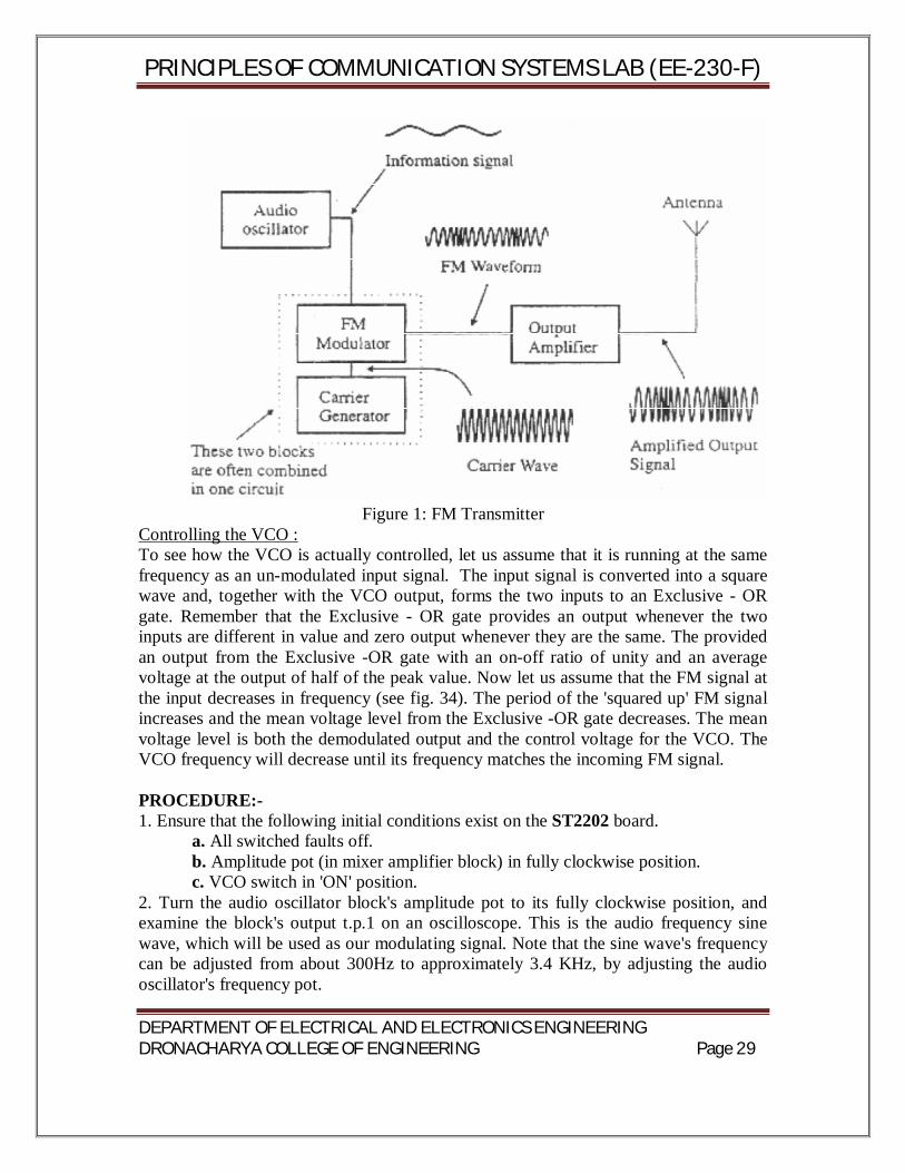
Analysis of FM waveforms Wave forms of carrier, modulating signal, modulated signal as well as graphical form of plot of Jn (mf) versus values of mf are shown below. It can be seen that : 1. Unlike AM, FM output contains carrier component of frequency fc as well as infinite number of side bands separated from the carrier frequency by fm, 2fc, 3fc,…….and thus have a recurrence frequency of fm. 2. The values of each Jn coefficient, which represent the amplitude of a pair of side bands, fluctuates on either side of zero, gradually diminishes with increasing value of mf like damped oscillations. The values of Jn coefficients also eventually decrease, but only past increased value of n. As the value of mf increases, the value of J0 decreases from 1 and the values of J1 to Jn increases from 0 and fluctuate around mean value of 0. 3. The modulation index determines how many side band components have significant values. 4. Unlike AM, in FM, while the amplitude of modulated signal remains constant, the value of the carrier component decreases with increase in mf like a damped oscillation. It means that while the total transmitted power remains constant in FM, the number side bands of significant amplitude (and therefore the effective band width) increase with increase in mf .This increases the immunity to noise in FM unlike AM. 5. As the value of mf increases, The carrier component becomes zero for certain values of modulation index, called eigen values which are approximately 2.4,5.5.8.6.11.8 and so on. These disappearances of carrier for specific values of mf, form a handy basis for measuring deviation. BLOCK DIAGRAM:- The audio oscillator supplies the information signal and could, if we wish, be replaced by a microphone and AF amplifier to provide speech and music instead of the sine wave signals that we are using with ST2203. The FM modulator is used to combine the carrier wave and the information signal in much the same way as in the AM transmitter. The only difference in this case is that the generation of the carrier wave and the modulation process is carried out in the same block. It is not necessary to have the two processes in same block, but in our case, it is. The output amplifier increases the power in the signal before it is applied to the antenna for transmission just as it did in the corresponding block in the FM transmitter.
PRINCIPLES OF COMMUNICATION SYSTEMS LAB (EE-230-F)
DEPARTMENT OF ELECTRICAL AND ELECTRONICS ENGINEERING DRONACHARYA COLLEGE OF ENGINEERING Page 29
Figure 1: FM Transmitter
Controlling the VCO : To see how the VCO is actually controlled, let us assume that it is running at the same frequency as an un-modulated input signal. The input signal is converted into a square wave and, together with the VCO output, forms the two inputs to an Exclusive - OR gate. Remember that the Exclusive - OR gate provides an output whenever the two inputs are different in value and zero output whenever they are the same. The provided an output from the Exclusive -OR gate with an on-off ratio of unity and an average voltage at the output of half of the peak value. Now let us assume that the FM signal at the input decreases in frequency (see fig. 34). The period of the 'squared up' FM signal increases and the mean voltage level from the Exclusive -OR gate decreases. The mean voltage level is both the demodulated output and the control voltage for the VCO. The VCO frequency will decrease until its frequency matches the incoming FM signal. PROCEDURE:- 1. Ensure that the following initial conditions exist on the ST2202 board.
a. All switched faults off. b. Amplitude pot (in mixer amplifier block) in fully clockwise position. c. VCO switch in 'ON' position.
2. Turn the audio oscillator block's amplitude pot to its fully clockwise position, and examine the block's output t.p.1 on an oscilloscope. This is the audio frequency sine wave, which will be used as our modulating signal. Note that the sine wave's frequency can be adjusted from about 300Hz to approximately 3.4 KHz, by adjusting the audio oscillator's frequency pot.
PRINCIPLES OF COMMUNICATION SYSTEMS LAB (EE-230-F)
DEPARTMENT OF ELECTRICAL AND ELECTRONICS ENGINEERING DRONACHARYA COLLEGE OF ENGINEERING Page 30
3. Connect the output of audio oscillator to VCO section’s MOD In socket. 4. Turn ON the power supply. 5. Observe the modulating signal and modulated output at the VCO’s MOD OUT socket by using CRO. 4. Calculate mf = δ / fm. 5. Vary the modulating frequency keeping carrier freq constant and repeat steps 3 & 4. 6. Vary the carrier frequency keeping modulator freq constant and repeat steps 3 & 4. 7. Tabulate the results. OBSERVATION TABLE:- 1 2 3 4 5
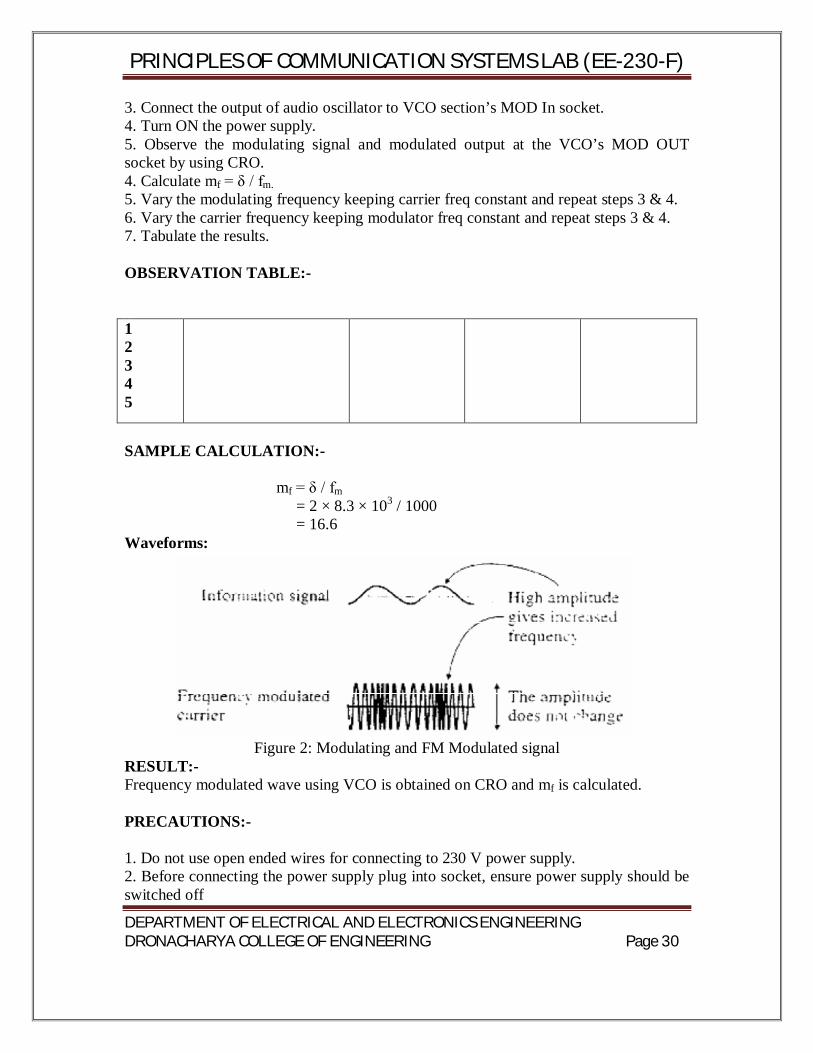
SAMPLE CALCULATION:- mf = δ / fm = 2 × 8.3 × 103 / 1000 = 16.6 Waveforms:
Figure 2: Modulating and FM Modulated signal
RESULT:- Frequency modulated wave using VCO is obtained on CRO and mf is calculated. PRECAUTIONS:- 1. Do not use open ended wires for connecting to 230 V power supply. 2. Before connecting the power supply plug into socket, ensure power supply should be switched off
PRINCIPLES OF COMMUNICATION SYSTEMS LAB (EE-230-F)
DEPARTMENT OF ELECTRICAL AND ELECTRONICS ENGINEERING DRONACHARYA COLLEGE OF ENGINEERING Page 31
3. Ensure all connections should be tight before switching on the power supply. 4. Take the reading carefully. 5. Power supply should be switched off after completion of experiment. QUIZ / ANSWERS:- Q.1. How many types of FM are there? Write their names. Ans. There two types of FM i.e. narrow band FM and wideband FM. Q.2. What frequency deviation in FM? Ans. The maximum change in instantaneous frequency from the average is known as frequency deviation. Q.3. Which is the useful parameter for determination of bandwidth? Ans. Frequency deviation is the useful parameter for determination of bandwidth. Q.4. How many sidebands are there in FM? Ans. Theoretically is infinite number sidebands in FM. Q.5. Which sidebands are ignored in FM? Ans. The sidebands with small amplitude are ignored in FM. Q.6. Which are significant sidebands? Ans. The sidebands having considerable amplitudes i.e. more than or equal to 1% of the carrier amplitude are known as significant sidebands. Q.7. what is CCIR? Ans. CCIR stands for Consultative Committee for International Radio. Q.8. What is the indirect method of FM generation? Ans. Armstrong method. Q.9. What is the direct method of FM generation? Ans. The parameter variation method. Q.10. What is VCO? Ans. VCO stands for voltage controlled oscillator whose frequency is controlled by modulating voltage.
PRINCIPLES OF COMMUNICATION SYSTEMS LAB (EE-230-F)
DEPARTMENT OF ELECTRICAL AND ELECTRONICS ENGINEERING DRONACHARYA COLLEGE OF ENGINEERING Page 32
EXPERIMENT 5 AIM: To generate FM signal using Varactor & reactance modulation. APPARATUS REQUIRED:
(i) C.R.O. (ii) CRO Probe (ii) FM Modulation and Demodulation Trainer (ST 2203) (iv) Connecting leads
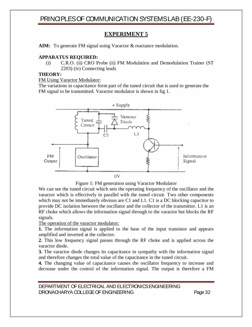
THEORY: FM Using Varactor Modulator: The variations in capacitance form part of the tuned circuit that is used to generate the FM signal to be transmitted. Varactor modulator is shown in fig 1.
Figure 1: FM generation using Varactor Modulator
We can see the tuned circuit which sets the operating frequency of the oscillator and the varactor which is effectively in parallel with the tuned circuit. Two other components which may not be immediately obvious are C1 and L1. C1 is a DC blocking capacitor to provide DC isolation between the oscillator and the collector of the transmitter. L1 is an RF choke which allows the information signal through to the varactor but blocks the RF signals. The operation of the varactor modulator: 1. The information signal is applied to the base of the input transistor and appears amplified and inverted at the collector. 2. This low frequency signal passes through the RF choke and is applied across the varactor diode. 3. The varactor diode changes its capacitance in sympathy with the information signal and therefore changes the total value of the capacitance in the tuned circuit. 4. The changing value of capacitance causes the oscillator frequency to increase and decrease under the control of the information signal. The output is therefore a FM
PRINCIPLES OF COMMUNICATION SYSTEMS LAB (EE-230-F)
DEPARTMENT OF ELECTRICAL AND ELECTRONICS ENGINEERING DRONACHARYA COLLEGE OF ENGINEERING Page 33
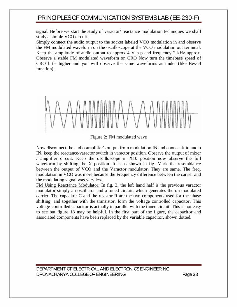
signal. Before we start the study of varactor/ reactance modulation techniques we shall study a simple VCO circuit. Simply connect the audio output to the socket labeled VCO modulation in and observe the FM modulated waveform on the oscilloscope at the VCO modulation out terminal. Keep the amplitude of audio output to approx 4 V p-p and frequency 2 kHz approx. Observe a stable FM modulated waveform on CRO Now turn the timebase speed of CRO little higher and you will observe the same waveforms as under (like Bessel function).
Figure 2: FM modulated wave
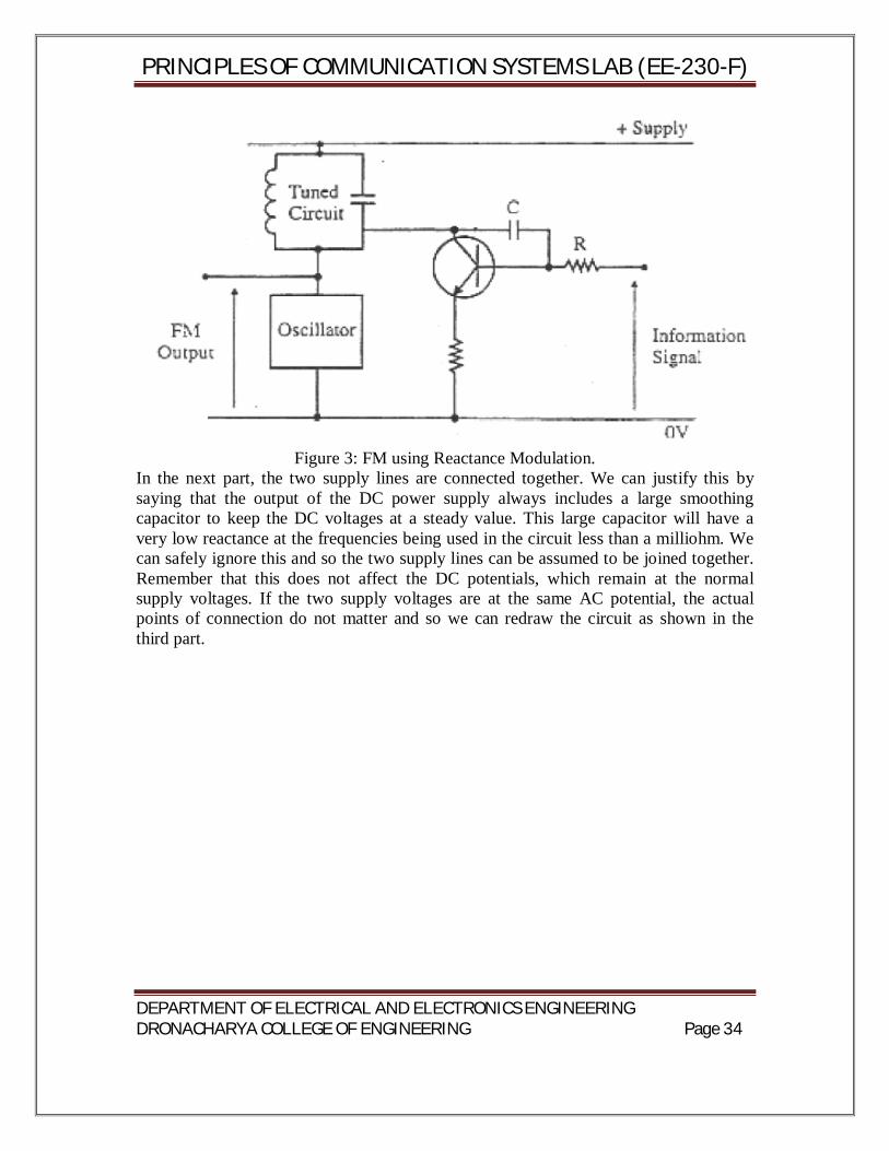
Now disconnect the audio amplifier's output from modulation IN and connect it to audio IN, keep the reactance/varactor switch in varactor position. Observe the output of mixer / amplifier circuit. Keep the oscilloscope in X10 position now observe the full waveform by shifting the X position. It is as shown in fig. Mark the resemblance between the output of VCO and the Varactor modulator. They are same. The freq. modulation in VCO was more because the Frequency difference between the carrier and the modulating signal was very less. FM Using Reactance Modulator: In fig. 3, the left hand half is the previous varactor modulator simply an oscillator and a tuned circuit, which generates the un-modulated carrier. The capacitor C and the resistor R are the two components used for the phase shifting, and together with the transistor, form the voltage controlled capacitor. This voltage-controlled capacitor is actually in parallel with the tuned circuit. This is not easy to see but figure 18 may be helpful. In the first part of the figure, the capacitor and associated components have been replaced by the variable capacitor, shown dotted.
PRINCIPLES OF COMMUNICATION SYSTEMS LAB (EE-230-F)
DEPARTMENT OF ELECTRICAL AND ELECTRONICS ENGINEERING DRONACHARYA COLLEGE OF ENGINEERING Page 34
Figure 3: FM using Reactance Modulation.
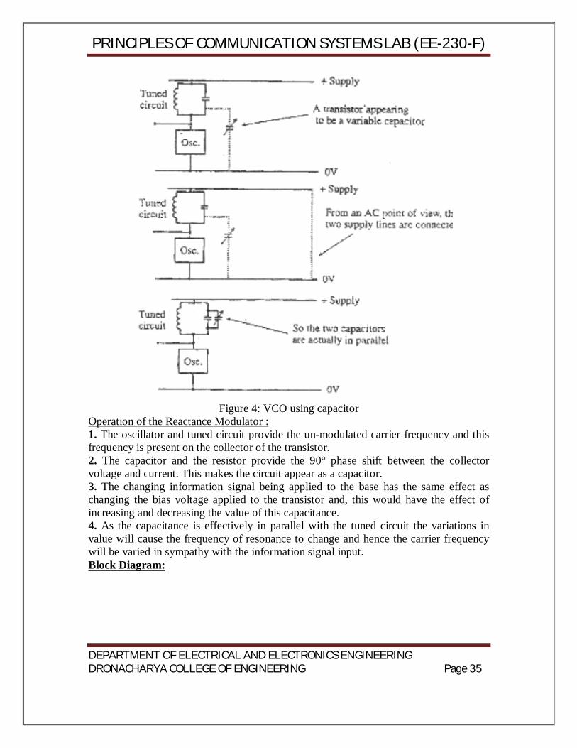
In the next part, the two supply lines are connected together. We can justify this by saying that the output of the DC power supply always includes a large smoothing capacitor to keep the DC voltages at a steady value. This large capacitor will have a very low reactance at the frequencies being used in the circuit less than a milliohm. We can safely ignore this and so the two supply lines can be assumed to be joined together. Remember that this does not affect the DC potentials, which remain at the normal supply voltages. If the two supply voltages are at the same AC potential, the actual points of connection do not matter and so we can redraw the circuit as shown in the third part.
PRINCIPLES OF COMMUNICATION SYSTEMS LAB (EE-230-F)
DEPARTMENT OF ELECTRICAL AND ELECTRONICS ENGINEERING DRONACHARYA COLLEGE OF ENGINEERING Page 35
Figure 4: VCO using capacitor
Operation of the Reactance Modulator : 1. The oscillator and tuned circuit provide the un-modulated carrier frequency and this frequency is present on the collector of the transistor. 2. The capacitor and the resistor provide the 90° phase shift between the collector voltage and current. This makes the circuit appear as a capacitor. 3. The changing information signal being applied to the base has the same effect as changing the bias voltage applied to the transistor and, this would have the effect of increasing and decreasing the value of this capacitance. 4. As the capacitance is effectively in parallel with the tuned circuit the variations in value will cause the frequency of resonance to change and hence the carrier frequency will be varied in sympathy with the information signal input. Block Diagram:
PRINCIPLES OF COMMUNICATION SYSTEMS LAB (EE-230-F)
DEPARTMENT OF ELECTRICAL AND ELECTRONICS ENGINEERING DRONACHARYA COLLEGE OF ENGINEERING Page 36
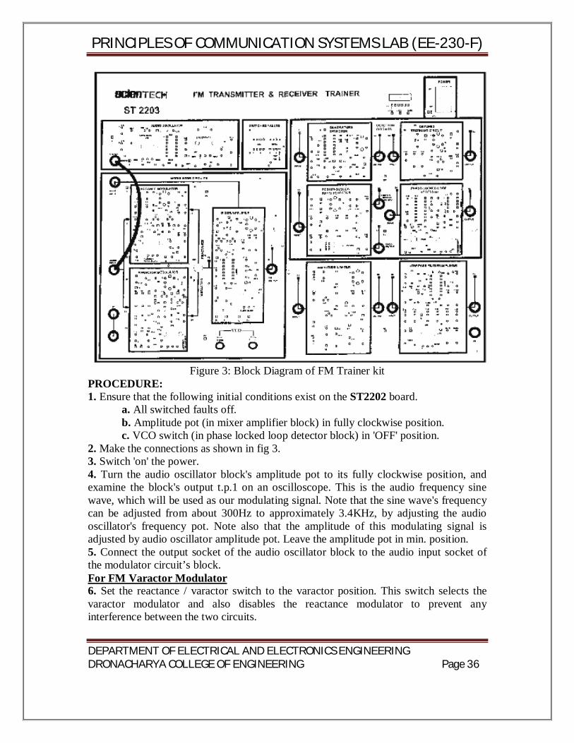
Figure 3: Block Diagram of FM Trainer kit
PROCEDURE: 1. Ensure that the following initial conditions exist on the ST2202 board.
a. All switched faults off. b. Amplitude pot (in mixer amplifier block) in fully clockwise position. c. VCO switch (in phase locked loop detector block) in 'OFF' position.
2. Make the connections as shown in fig 3. 3. Switch 'on' the power. 4. Turn the audio oscillator block's amplitude pot to its fully clockwise position, and examine the block's output t.p.1 on an oscilloscope. This is the audio frequency sine wave, which will be used as our modulating signal. Note that the sine wave's frequency can be adjusted from about 300Hz to approximately 3.4KHz, by adjusting the audio oscillator's frequency pot. Note also that the amplitude of this modulating signal is adjusted by audio oscillator amplitude pot. Leave the amplitude pot in min. position. 5. Connect the output socket of the audio oscillator block to the audio input socket of the modulator circuit’s block. For FM Varactor Modulator 6. Set the reactance / varactor switch to the varactor position. This switch selects the varactor modulator and also disables the reactance modulator to prevent any interference between the two circuits.
PRINCIPLES OF COMMUNICATION SYSTEMS LAB (EE-230-F)
DEPARTMENT OF ELECTRICAL AND ELECTRONICS ENGINEERING DRONACHARYA COLLEGE OF ENGINEERING Page 37
7. The output signal from the varactor modulator block appears at t.p. 24 before being buffered and amplified by the mixer / amplifier block, any capacitive loading (e.g. due to oscilloscope probe) may slightly affect the modulators output frequency. In order to avoid this problem we monitor the buffered FM output signal the mixer / amplifier block at t.p.34. 8. Put the varactor modulator's carrier frequency pot in its midway position, and then examine t.p. 34. Note that it is a sine wave of approximately 1.2 Vp-p, centered on 0V. This is our FM carrier, and it is un-modulated since the varactor modulators audio input signal has zero amplitude. 9. The amplitude of the FM carrier (at t.p.34) is adjustable by means of the mixer/amplifier block's amplitude pot, from zero to its pot level. Try turning this pot slowly anticlockwise, and note that the amplitude of the FM signal can be reduced to zero. Return the amplitude pot to its fully clockwise position. 10. Try varying the carrier frequency pot and observe the effects. 11. Also, see the effects of varying the amplitude and frequency pots in the audio oscillator block. 12. Turn the carrier frequency pot in the varactor modulator block slowly clockwise and note that in addition to the carrier frequency increasing there is a decrease in the amount of frequency deviation that is present. 13. Return the carrier frequency pot to its midway position, and monitor the audio input (at t.p.6) and the FM output (at p.34) triggering the oscilloscope on the audio input signal. Turn the audio oscillator's amplitude pot throughout its range of adjustment, and note that the amplitude of the FM output signal does not change. This is because the audio information is contained entirely in the signals frequency and not in its amplitude. 14. By using the optional audio input module ST2108 the human voice can be used as the audio modulating signal, instead of using ST2203's audio oscillator block. If you have an audio input module, connect the module's output to the audio input socket in the modulator circuit’s block. The input signal to the audio input module may be taken from an external microphone be (supplied with the module) or from a cassette recorder, by choosing the appropriate switch setting on the module. For FM Reactance Modulator: 6. Put the reactance /varactor switch in the reactance position. This switches the output of the reactance modulator through to the input of the mixer/amplifier block ~ and also switches off the varactor modulator block to avoid interference between the two modulators. 7. The output signal from the reactance modulator block appears at tp.13, before being buffered and amplified by the mixer/amplifier block. Although the output from the reactance modulator block can be monitored directly at tp.13, any capacitive loading affect this point (e.g. due to an oscilloscope probe) may slightly affect the modulator's output frequency. In order to avoid this problem we will monitor the buffered FM output signal from the mixer/amplifier block at t.p. 34. 8. Put the reactance modulator's pot in its midway position (arrow pointing towards top of PCB) then examine t.p. 34. Note that the monitored signal is a sine wave of
PRINCIPLES OF COMMUNICATION SYSTEMS LAB (EE-230-F)
DEPARTMENT OF ELECTRICAL AND ELECTRONICS ENGINEERING DRONACHARYA COLLEGE OF ENGINEERING Page 38
approximately 1.2V peak/peak centered on 0 volts D.C. This is our FM carrier, and it is presently un-modulated since the reactance modulator's audio input signal has, zero amplitude. 9. The amplitude of the FM carrier (at t.p.34) is adjustable by means of the mixer/amplifier block's amplitude pot, from zero to its present level. Try turning this pot slowly anticlockwise, and note that the amplitude of the FM signal can be reduced to zero. Return the amplitude pot to its fully clockwise position. 10. The frequency of the FM carrier signal (at t.p.34) should be approximately 455Khz at the moment This carrier frequency can be varied from 453Khz to 460Khz (approx.) by adjusting the carrier frequency pot in the reactance modulator block. Turn this pot over its range of adjustment and note that the frequency of the monitored signal can be seen to vary slightly. Note also that the carrier frequency is maximum when the pot is in fully clockwise position. 11. Try varying the amplitude & frequency pot in audio oscillators block, and also sees the effect of varying the carrier frequency pot in the mixer/amplifiers block. 12. Monitor the audio input (at t.p.6) and the FM output (at t.p.34) triggering the oscilloscope on the audio input signal. Turn the audio oscillator's amplitude pot throughout its range of adjustment and note that the amplitude of the FM output signal does not change. This is because the audio information is contained entirely in the signal's frequency, and not in its amplitude. RESULT:- Frequency modulated signal is generated by using varactor and reactance modulator. PRECAUTIONS:- 1. Do not use open ended wires for connecting to 230 V power supply. 2. Before connecting the power supply plug into socket, ensure power supply should be switched off 3. Ensure all connections should be tight before switching on the power supply. 4. Take the reading carefully. QUIZ / ANSWERS:- Q.1. How many types of FM are there? Write their names. Ans. There two types of FM i.e. narrow band FM and wideband FM. Q.2. What frequency deviation in FM? Ans. The maximum change in instantaneous frequency from the average is known as frequency deviation. Q.3. Which is the useful parameter for determination of bandwidth? Ans. Frequency deviation is the useful parameter for determination of bandwidth. Q.4. How many sidebands are there in FM? Ans. Theoretically is infinite number sidebands in FM. Q.5. Which sidebands are ignored in FM? Ans. The sidebands with small amplitude are ignored in FM.
PRINCIPLES OF COMMUNICATION SYSTEMS LAB (EE-230-F)
DEPARTMENT OF ELECTRICAL AND ELECTRONICS ENGINEERING DRONACHARYA COLLEGE OF ENGINEERING Page 39
Q.6. Which are significant sidebands? Ans. The sidebands having considerable amplitudes i.e. more than or equal to 1% of the carrier amplitude are known as significant sidebands. Q.7. what is CCIR? Ans. CCIR stands for Consultative Committee for International Radio. Q.8. What is the indirect method of FM generation? Ans. Armstrong method.
PRINCIPLES OF COMMUNICATION SYSTEMS LAB (EE-230-F)
DEPARTMENT OF ELECTRICAL AND ELECTRONICS ENGINEERING DRONACHARYA COLLEGE OF ENGINEERING Page 40
EXPERIMENT 6 AIM: To Detect FM Signal using PLL & Foster-Seelay method. APPARATUS REQUIRED:
(i) C.R.O. (ii) CRO Probe (ii) FM Modulation and Demodulation Trainer (ST 2203) (iv) Connecting leads
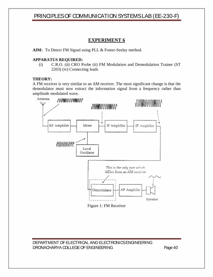
THEORY: A FM receiver is very similar to an AM receiver. The most significant change is that the demodulator must now extract the information signal from a frequency rather than amplitude modulated wave.
Figure 1: FM Receiver
PRINCIPLES OF COMMUNICATION SYSTEMS LAB (EE-230-F)
DEPARTMENT OF ELECTRICAL AND ELECTRONICS ENGINEERING DRONACHARYA COLLEGE OF ENGINEERING Page 41
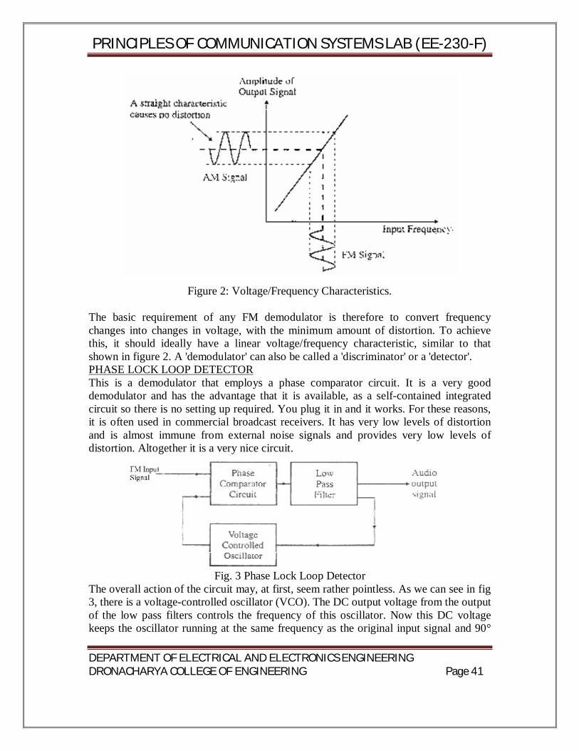
Figure 2: Voltage/Frequency Characteristics.
The basic requirement of any FM demodulator is therefore to convert frequency changes into changes in voltage, with the minimum amount of distortion. To achieve this, it should ideally have a linear voltage/frequency characteristic, similar to that shown in figure 2. A 'demodulator' can also be called a 'discriminator' or a 'detector'. PHASE LOCK LOOP DETECTOR This is a demodulator that employs a phase comparator circuit. It is a very good demodulator and has the advantage that it is available, as a self-contained integrated circuit so there is no setting up required. You plug it in and it works. For these reasons, it is often used in commercial broadcast receivers. It has very low levels of distortion and is almost immune from external noise signals and provides very low levels of distortion. Altogether it is a very nice circuit.
Fig. 3 Phase Lock Loop Detector
The overall action of the circuit may, at first, seem rather pointless. As we can see in fig 3, there is a voltage-controlled oscillator (VCO). The DC output voltage from the output of the low pass filters controls the frequency of this oscillator. Now this DC voltage keeps the oscillator running at the same frequency as the original input signal and 90°
PRINCIPLES OF COMMUNICATION SYSTEMS LAB (EE-230-F)
DEPARTMENT OF ELECTRICAL AND ELECTRONICS ENGINEERING DRONACHARYA COLLEGE OF ENGINEERING Page 42
out of phase. And if we did, then why not just add a phase shifting circuit at the input to give the 90° phase shift? The answer can be seen by imagining what happens when the input frequency changes - as it would with a FM signal. If the input frequency increases and decreases, the VCO frequency is made to follow it. To do this, the input control voltage must increase and decrease. These change of DC voltage level that forms the demodulated signal. The AM signal then passes through a signal buffer to prevent any loading effects from disturbing the VCO and then through an audio amplifier if necessary. The frequency response is highly linear as shown in figure 2. FOSTER SEELEY DETECTOR The foster Seeley circuit is shown in fig. 4. At first glance, it looks rather complicated but it becomes simpler if we consider it a bit at a time.
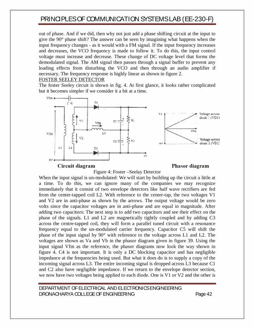
Figure 4: Foster –Seelay Detector
When the input signal is un-modulated: We will start by building up the circuit a little at a time. To do this, we can ignore many of the companies we may recognize immediately that it consist of two envelope detectors like half wave rectifiers are fed from the center-tapped coil L2. With reference to the center-tap, the two voltages V1 and V2 are in anti-phase as shown by the arrows. The output voltage would be zero volts since the capacitor voltages are in anti-phase and are equal in magnitude. After adding two capacitors: The next step is to add two capacitors and see their effect on the phase of the signals. L1 and L2 are magnetically tightly coupled and by adding C3 across the centre-tapped coil, they will form a parallel tuned circuit with a resonance frequency equal to the un-modulated carrier frequency. Capacitor C5 will shift the phase of the input signal by 90° with reference to the voltage across L1 and L2. The voltages are shown as Va and Vb in the phasor diagram given in figure 39. Using the input signal Vfm as the reference, the phasor diagrams now look the way shown in figure 4. C4 is not important. It is only a DC blocking capacitor and has negligible impedance at the frequencies being used. But what it does do is to supply a copy of the incoming signal across L3. The entire incoming signal is dropped across L3 because C1 and C2 also have negligible impedance. If we return to the envelope detector section, we now have two voltages being applied to each diode. One is V1 or V2 and the other is
PRINCIPLES OF COMMUNICATION SYSTEMS LAB (EE-230-F)
DEPARTMENT OF ELECTRICAL AND ELECTRONICS ENGINEERING DRONACHARYA COLLEGE OF ENGINEERING Page 43
the new voltage across L3, which is equal to Vfm. When the input Frequency changes: If the input frequency increased above its un-modulated value, the phasor of Va would fall below 90° due to the parallel tuned circuit becoming increasingly capacitive. This would result in a larger total voltage being applied across D1 and a reduced voltage across D2. Since the capacitor C1 would now charge to a higher voltage, the final output from the circuit would be a positive voltage. Conversely, if the frequency of the FM input signal decreased below the unmodulated value, the phase shift due to capacitor C5 increases above 90° as the parallel tuned circuit becomes slightly inductive. This causes the voltage across diode D2 to increase and the final output from the demodulator becomes negative. The effect of noise is to change the amplitude of the incoming FM signal resulting in a proportional increase and decrease in the amplitude of diode voltages VD1 and VD2 and the difference in voltage is the demodulated output, the circuit is susceptible to noise interference and should be preceded by a noise limiter circuit. BLOCK DIAGRAM:
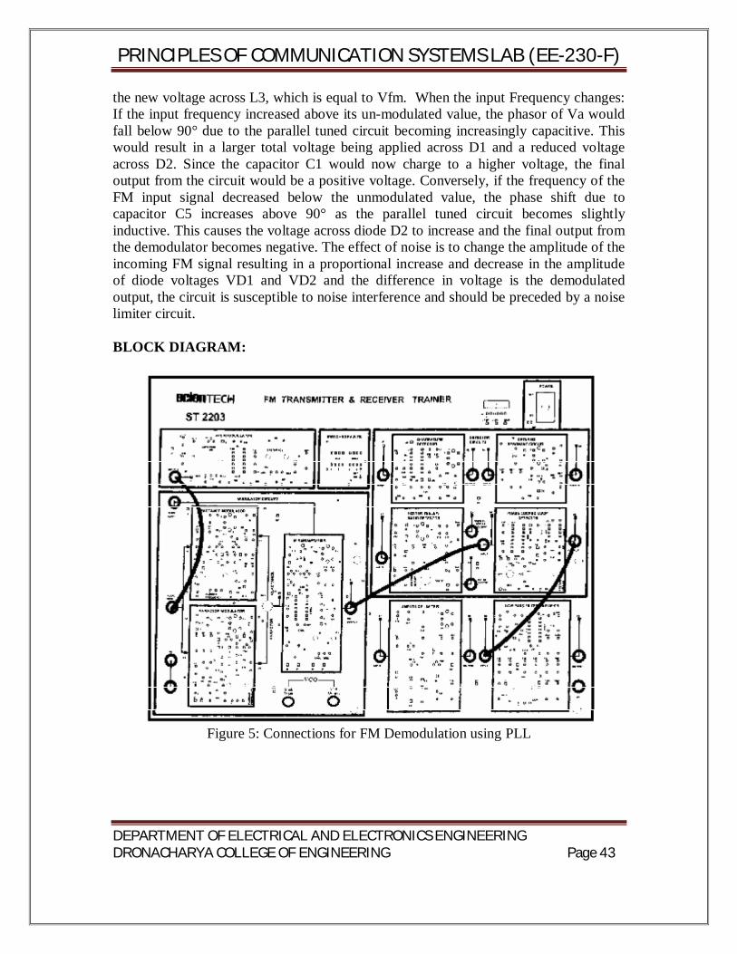
Figure 5: Connections for FM Demodulation using PLL
PRINCIPLES OF COMMUNICATION SYSTEMS LAB (EE-230-F)
DEPARTMENT OF ELECTRICAL AND ELECTRONICS ENGINEERING DRONACHARYA COLLEGE OF ENGINEERING Page 44
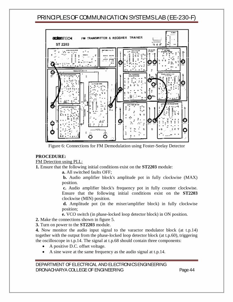
Figure 6: Connections for FM Demodulation using Foster-Seelay Detector
PROCEDURE: FM Detection using PLL: 1. Ensure that the following initial conditions exist on the ST2203 module: a. All switched faults OFF;
b. Audio amplifier block's amplitude pot in fully clockwise (MAX) position. c. Audio amplifier block's frequency pot in fully counter clockwise. Ensure that the following initial conditions exist on the ST2203 clockwise (MIN) position. d. Amplitude pot (in the mixer/amplifier block) in fully clockwise position;
e. VCO switch (in phase-locked loop detector block) in ON position. 2. Make the connections shown in figure 5. 3. Turn on power to the ST2203 module. 4. Now monitor the audio input signal to the varactor modulator block (at t.p.14) together with the output from the phase-locked loop detector block (at t.p.60), triggering the oscilloscope in t.p.14. The signal at t.p.68 should contain three components:
A positive D.C. offset voltage. A sine wave at the same frequency as the audio signal at t.p.14.
PRINCIPLES OF COMMUNICATION SYSTEMS LAB (EE-230-F)
DEPARTMENT OF ELECTRICAL AND ELECTRONICS ENGINEERING DRONACHARYA COLLEGE OF ENGINEERING Page 45
A high - frequency ripple component. 5. The low pass filter/amplifier block strongly attenuates the high-frequency ripple component at the detector's output and also blocks the D.C. offset voltage. Consequently the signal at the output of the low- pass filter/amplifier block (at t.p.73) should be very closely resemble the original audio making signal, if not then slowly adjust the freq. adjust pot of PLL block. 6. Adjust the audio oscillator block's amplitude and frequency pots, and compare the original audio signal with the final demodulated signal. FM Detection using Foster-Seelay Detector: 1. Ensure that the following initial conditions exist on the ST2203 module: a. All switched faults OFF;
b. Audio amplifier block's amplitude pot in fully clockwise (MAX) position. c. Audio amplifier block's frequency pot in fully counter-clockwise (MIN) position. d. Amplitude pot (in the mixer/amplifier block) in fully clockwise position.
e. VCO switch (in phase-locked loop detector block) in OFF position. 2. Make connection as shown in figure 42 3. Turn on power to the ST2203 module. 4. We will now investigate the operation of the foster-Seeley detector on the ST2203 module. In the Foster-Seeley / ratio detector block, select the Foster-Seeley detector by putting the switch in the Foster-Seeley position. 5. Initially, we will use the varactor modulator to generate our FM signal, since this is the more linear of the two modulators, as fast as its frequency/voltage characteristic is concerned. To select the varactor modulator, put the reactance/ varactor switch in the varactor position. Ensure that the varactor modulator's carrier frequency pot is in the midway position. 6. The audio oscillator's output signal (which appears at t.p.1) is now being used by the varactor modulator, to frequency-modulate a 455Khz carrier sine wave. As we saw earlier, this FM waveform appears at the FM output socket from the mixer/amplifier block. You will probably need to have an X-expansion control on your oscilloscope. 7. Now monitor the audio input signal to the varactor modulator block (at t.p. 14) together with the foster-seeley output from the foster-seeley/ratio detector block (at t.p. 52), triggering the oscilloscope on t.p. 14. The signal at t.p. 52 should contain two components: · A sine wave at the same frequency as the audio signal at t.p. 14. · A High frequency ripple component of small amplitude. 8. The low-pass filter/amplifier strongly attenuates this high-frequency ripple component, and blocks any small D.C. offset voltage that might exist at the detector's output. Consequently, the signal at the output of the low-pass filter/ amplifier block (at t.p. 73) should very closely resemble the original audio modulating signal.
PRINCIPLES OF COMMUNICATION SYSTEMS LAB (EE-230-F)
DEPARTMENT OF ELECTRICAL AND ELECTRONICS ENGINEERING DRONACHARYA COLLEGE OF ENGINEERING Page 46
9. Monitor the audio input to the varactor modulator (at t.p. 14) and the output of the low pass filter / amplifier block (at t.p. 73) and adjust the gain pot (in the low pass filter/ amplifier block) until the amplitudes of the monitored audio waveforms are the same. 10. Adjust the audio oscillator block's amplitude and frequency pots, and compare the original audio signal with the final demodulated signal. RESULT:- FM signal is being demodulated by using PLL and Foster-Seelay Method. PRECAUTIONS:- 1. Do not use open ended wires for connecting to 230 V power supply. 2. Before connecting the power supply plug into socket, ensure power supply should be switched off 3. Ensure all connections should be tight before switching on the power supply. 4. Take the reading carefully. 5. Power supply should be switched off after completion of experiment. QUIZ / ANSWERS:- Q.1. How many types of FM are there? Write their names. Ans. There two types of FM i.e. narrow band FM and wideband FM. Q.2. What frequency deviation in FM? Ans. The maximum change in instantaneous frequency from the average is known as frequency deviation. Q.3. Which is the useful parameter for determination of bandwidth? Ans. Frequency deviation is the useful parameter for determination of bandwidth. Q.4. How many sidebands are there in FM? Ans. Theoretically is infinite number sidebands in FM. Q.5. Which sidebands are ignored in FM? Ans. The sidebands with small amplitude are ignored in FM. Q.6. Which are significant sidebands? Ans. The sidebands having considerable amplitudes i.e. more than or equal to 1% of the carrier amplitude are known as significant sidebands. Q.7. what is CCIR? Ans. CCIR stands for Consultative Committee for International Radio. Q.8. What is the indirect method of FM generation? Ans. Armstrong method. Q.9. What is the direct method of FM generation? Ans. The parameter variation method.
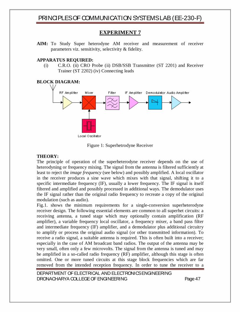
PRINCIPLES OF COMMUNICATION SYSTEMS LAB (EE-230-F)
DEPARTMENT OF ELECTRICAL AND ELECTRONICS ENGINEERING DRONACHARYA COLLEGE OF ENGINEERING Page 47
EXPERIMENT 7 AIM: To Study Super heterodyne AM receiver and measurement of receiver
parameters viz. sensitivity, selectivity & fidelity. APPARATUS REQUIRED:
(i) C.R.O. (ii) CRO Probe (ii) DSB/SSB Transmitter (ST 2201) and Receiver Trainer (ST 2202) (iv) Connecting leads
BLOCK DIAGRAM:
Figure 1: Superhetrodyne Receiver
THEORY: The principle of operation of the superheterodyne receiver depends on the use of heterodyning or frequency mixing. The signal from the antenna is filtered sufficiently at least to reject the image frequency (see below) and possibly amplified. A local oscillator in the receiver produces a sine wave which mixes with that signal, shifting it to a specific intermediate frequency (IF), usually a lower frequency. The IF signal is itself filtered and amplified and possibly processed in additional ways. The demodulator uses the IF signal rather than the original radio frequency to recreate a copy of the original modulation (such as audio). Fig.1. shows the minimum requirements for a single-conversion superheterodyne receiver design. The following essential elements are common to all superhet circuits: a receiving antenna, a tuned stage which may optionally contain amplification (RF amplifier), a variable frequency local oscillator, a frequency mixer, a band pass filter and intermediate frequency (IF) amplifier, and a demodulator plus additional circuitry to amplify or process the original audio signal (or other transmitted information). To receive a radio signal, a suitable antenna is required. This is often built into a receiver; especially in the case of AM broadcast band radios. The output of the antenna may be very small, often only a few microvolts. The signal from the antenna is tuned and may be amplified in a so-called radio frequency (RF) amplifier, although this stage is often omitted. One or more tuned circuits at this stage block frequencies which are far removed from the intended reception frequency. In order to tune the receiver to a
PRINCIPLES OF COMMUNICATION SYSTEMS LAB (EE-230-F)
DEPARTMENT OF ELECTRICAL AND ELECTRONICS ENGINEERING DRONACHARYA COLLEGE OF ENGINEERING Page 48
particular station, the frequency of the local oscillator is controlled by the tuning knob (for instance). Tuning of the local oscillator and the RF stage may use a variable capacitor, or varicap diode. The tuning of one (or more) tuned circuits in the RF stage must track the tuning of the local oscillator. Mixer stage:The signal is then fed into a circuit where it is mixed with a sine wave from a variable frequency oscillator known as the local oscillator (LO). The mixer uses a non-linear component to produce both sum and difference beat frequencies signals, each one containing the modulation contained in the desired signal. The output of the mixer may include the original RF signal at fd, the local oscillator signal at fLO, and the two new frequencies fd+fLO and fd-fLO. The mixer may inadvertently produce additional frequencies such as 3rd- and higher-order intermodulation products. The undesired signals are removed by the IF bandpass filter, leaving only the desired offset IF signal at fIF which contains the original modulation (transmitted information) as the received radio signal had at fd. Intermediate frequency stage:The stages of an intermediate frequency amplifier are tuned to a particular frequency not dependent on the receiving frequency; this greatly simplifies optimization of the circuit.[6] The IF amplifier (or IF strip) can be made highly selective around its center frequency fIF, whereas achieving such a selectivity at a much higher RF frequency would be much more difficult. By tuning the frequency of the local oscillator fLO, the resulting difference frequency fLO - fd (or fd-fLO when using so-called low-side injection) will be matched to the IF amplifier's frequency fIF for the desired reception frequency fd. One section of the tuning capacitor will thus adjust the local oscillator's frequency fLO to fd + fIF (or. less often, to fd - fIF) while the RF stage is tuned to fd. Engineering the multi-section tuning capacitor (or varactors) and coils to fulfill this condition across the tuning range is known as tracking. Other signals produced by the mixer (such as due to stations at nearby frequencies) can be very well filtered out in the IF stage, giving the superheterodyne receiver its superior performance. However, if fLO is set to fd + fIF , then an incoming radio signal at fLO + fIF will also produce a heterodyne at fIF; this is called the image frequency and must be rejected by the tuned circuits in the RF stage. The image frequency is 2fIF higher (or lower) than fd, so employing a higher IF frequency fIF increases the receiver's image rejection without requiring additional selectivity in the RF stage. Usually the intermediate frequency is lower than the reception frequency fd, but in some modern receivers (e.g. scanners and spectrum analyzers) it is more convenient to first convert an entire band to a much higher intermediate frequency; this eliminates the problem of image rejection. Then a tunable local oscillator and mixer convert that signal to a second much lower intermediate frequency where the selectivity of the receiver is accomplished. In order to avoid interference to receivers, licensing authorities will avoid assigning common IF frequencies to transmitting stations. Standard intermediate frequencies used are 455 kHz for medium-wave AM radio, 10.7 MHz for broadcast FM receivers, 38.9 MHz (Europe) or 45 MHz (US) for television, and 70 MHz for satellite and terrestrial microwave equipment.
PRINCIPLES OF COMMUNICATION SYSTEMS LAB (EE-230-F)
DEPARTMENT OF ELECTRICAL AND ELECTRONICS ENGINEERING DRONACHARYA COLLEGE OF ENGINEERING Page 49
Bandpass filter :The IF stage includes a filter and/or multiple tuned circuits in order to achieve the desired selectivity. This filtering must therefore have a band pass equal to or less than the frequency spacing between adjacent broadcast channels. Ideally a filter would have a high attenuation to adjacent channels, but maintain a flat response across the desired signal spectrum in order to retain the quality of the received signal. This may be obtained using one or more dual tuned IF transformers or a multipole ceramic crystal filter.
Demodulation:The received signal is now processed by the demodulator stage where the audio signal (or other baseband signal) is recovered and then further amplified. AM demodulation requires the simple rectification of the RF signal (so-called envelope detection), and a simple RC low pass filter to remove remnants of the intermediate frequency. FM signals may be detected using a discriminator, ratio detector, or phase-locked loop. Continuous wave (morse code) and single sideband signals require a product detector using a so-called beat frequency oscillator, and there are other techniques used for different types of modulation. The resulting audio signal (for instance) is then amplified and drives a loudspeaker. When so-called high-side injection has been used, where the local oscillator is at a higher frequency than the received signal (as is common), then the frequency spectrum of the original signal will be reversed. This must be taken into account by the demodulator (and in the IF filtering) in the case of certain types of modulation such as single sideband. RECEIVER CHARACTERISTICS: The important characteristics of receivers are sensitivity, selectivity, & fidelity described as follows: Sensitivity: The sensitivity of radio receiver is that characteristic which determines the minimum strength of signal input capable of causing a desired value of signal output. Therefore, expressing in terms of voltage or power, sensitivity can be defined as the minimum voltage or power at the receiver input for causing a standard output. In case of amplitude-modulation broadcast receivers, the definition of sensitivity has been standardized as "amplitude of carrier voltage modulated 30% at 400 cycles, which when applied to the receiver input terminals through a standard dummy antenna will develop an output of 0.5 watt in a resistance load of appropriate value substituted for the loud speaker" . Selectivity: The selectivity of a radio receiver is that characteristic which determines the extent to which it is capable of differentiating between the desired signal and signal of other frequencies. Fidelity: This is defined as the degree with which a system accurately reproduces at its output the essential characteristics of signals which is impressed upon its input.
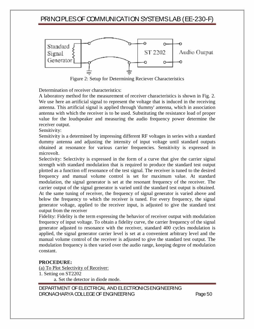
PRINCIPLES OF COMMUNICATION SYSTEMS LAB (EE-230-F)
DEPARTMENT OF ELECTRICAL AND ELECTRONICS ENGINEERING DRONACHARYA COLLEGE OF ENGINEERING Page 50
Figure 2: Setup for Determining Reciever Characteristics
Determination of receiver characteristics: A laboratory method for the measurement of receiver characteristics is shown in Fig. 2. We use here an artificial signal to represent the voltage that is induced in the receiving antenna. This artificial signal is applied through 'dummy' antenna, which in association antenna with which the receiver is to be used. Substituting the resistance load of proper value for the loudspeaker and measuring the audio frequency power determine the receiver output. Sensitivity: Sensitivity is a determined by impressing different RF voltages in series with a standard dummy antenna and adjusting the intensity of input voltage until standard outputs obtained at resonance for various carrier frequencies. Sensitivity is expressed in microvolt. Selectivity: Selectivity is expressed in the form of a curve that give the carrier signal strength with standard modulation that is required to produce the standard test output plotted as a function off resonance of the test signal. The receiver is tuned to the desired frequency and manual volume control is set for maximum value. At standard modulation, the signal generator is set at the resonant frequency of the receiver. The carrier output of the signal generator is varied until the standard test output is obtained. At the same tuning of receiver, the frequency of signal generator is varied above and below the frequency to which the receiver is tuned. For every frequency, the signal generator voltage, applied to the receiver input, is adjusted to give the standard test output from the receiver Fidelity: Fidelity is the term expressing the behavior of receiver output with modulation frequency of input voltage. To obtain a fidelity curve, the carrier frequency of the signal generator adjusted to resonance with the receiver, standard 400 cycles modulation is applied, the signal generator carrier level is set at a convenient arbitrary level and the manual volume control of the receiver is adjusted to give the standard test output. The modulation frequency is then varied over the audio range, keeping degree of modulation constant. PROCEDURE: (a) To Plot Selectivity of Receiver: 1. Setting on ST2202
a. Set the detector in diode mode.
PRINCIPLES OF COMMUNICATION SYSTEMS LAB (EE-230-F)
DEPARTMENT OF ELECTRICAL AND ELECTRONICS ENGINEERING DRONACHARYA COLLEGE OF ENGINEERING Page 51
b. AGC on. c. Set the volume control full clockwise.
2. Apply AM signal with 400 Hz modulating frequency and 30% modulation taken from AM generator into Rx input socket. 3. Set the input carrier frequency to suitable value that lies within the AM band (525 KHz - 1600 KHz). Also set signal level to 100mV. 4. Tune the Receiver using tuning control. Also adjust gain potentiometer provided in R.F. amplifier section of ST2202 so as to get unclipped demodulated signal at detector's output (output of audio amplifier). 5. Note the voltage level at receiver's final output stage i.e. audio amplifier's output on CRO (voltage at resonance (Vr)). 6. Now gradually offset the carrier frequency in suitable steps of 5 KHz or 10 KHz below and above the frequency adjusted in step 2 without changing the tuning of receiver while maintaining the input signal level. 7. Now record the signal level at output of audio amplifier for different input carrier frequency, on CRO (i.e. voltage off resonance (Vi)). 8. Tabulate the readings as under:
9. Plot the curve between ratio and carrier frequency. (b) To Plot Sensitivity of Receiver: 1. Setting on ST2202 :
a. Set the detector in diode mode. b. AGC on. c. Set the volume control fully clockwise.
2. Apply AM signal, with 400 Hz modulating signal and 30% modulation, taken from AM generator into Rx input socket. 3. Set the input carrier frequency so as to lie within the AM Band (525 KHz – 1600 KHz). Also tune the detector to that carrier frequency using tuning control.(You will hear atone) 4. Set the input AM level to 100 mV. Also adjust the gain potentiometer provided in R.F. amplifier section of ST2202 so as to get unclipped demodulated signal at detectors output. 5. Record input carrier frequency & signal level at the final output stage i.e. output of audio amplifier (observed on CRO). 6. Change the input carrier frequency & also tune the receiver to that frequency & repeat step 4. 7. Tabulate the collected readings as under:
PRINCIPLES OF COMMUNICATION SYSTEMS LAB (EE-230-F)
DEPARTMENT OF ELECTRICAL AND ELECTRONICS ENGINEERING DRONACHARYA COLLEGE OF ENGINEERING Page 52
8. Plot the graph between carrier frequency & output level. (c) To Plot Fidelity of Receiver: 1. Setting on ST220 :
a. Set the detector in diode mode. b. AGC on. c. Set the volume control fully clockwise.
2. Apply AM signal of 100mV with 400Hz modulating signal and 30% modulation, into Rx input. 3. Select a suitable carrier frequency that lies within AM Band (525 KHz - 1600 KHz). Tune the ST2202 receiver to that frequency using tuning control. Also adjust gain potentiometer provided in R.F. amplifier section so as to get unclipped demodulated signal at detector's output. 4. Note the demodulated signal level (Vr) at the final output stage i.e. output of audio amplifier (on CRO) for the applied AM signal with 400Hz modulating signal. 5. Now vary the modulating signal frequency over audio range (300 Hz-3 KHz) in suitable steps say 100Hz. Note the corresponding output level (Vi) at the output of audio amplifier (on CRO). 6. Tabulate readings as under:
Relative response = 20 log (Vi / Vr) dB
7. Plot the graph between modulating frequency and relative response. RESULT:- Superhetrodyne receiver has been studied and plot for receiver parameters viz. sensitivity, selectivity and fidelity has been drawn. PRECAUTIONS:- 1. Do not use open ended wires for connecting to 230 V power supply. 2. Before connecting the power supply plug into socket, ensure power supply should be switched off 3. Ensure all connections should be tight before switching on the power supply. 4. Take the reading carefully. 5. Power supply should be switched off after completion of experiment.
PRINCIPLES OF COMMUNICATION SYSTEMS LAB (EE-230-F)
DEPARTMENT OF ELECTRICAL AND ELECTRONICS ENGINEERING DRONACHARYA COLLEGE OF ENGINEERING Page 53
EXPERIMENT 8 (a) AIM:-To study Pulse Amplitude Modulation. APPARATUS REQUIRED:- CRO, experimental kit, power supply, connecting leads. BRIEF THEORY:- Pulse Modulation: We know that in Analog modulation systems, some parameter of a sinusoidal carrier (continuous in time domain) is varied according to the instantaneous value of the modulating signal. But in pulse modulation methods, the carrier is no longer a continuous signal but consists of a train of uniform pulses having a defined PRF (Pulse Repetition Frequency). The continuous modulating message signal waveforms are sampled at regular intervals. Information regarding the signal is transmitted only at the sampling times, together with any synchronizing pulses that may be required. At the receiving end, the original wave form may be reconstituted with negligible distortion from the information regarding the samples, if these samples are taken with minimum sufficient frequency. In Pulse Modulation some parameter of the pulsed carrier is varied according to the instantaneous value of the modulating signal. Pulse modulation may be broadly subdivided into two categories: Analog & Digital. In the former, the indication of sample amplitude may be infinitely variable, while in the latter a code which indicates the sample amplitude to the nearest pre-determined level is sent. Pulse-Amplitude & Pulse-Time Modulation are both analog while the Pulse-code and Delta modulation are both digital. All the modulation systems have sampling in common, but they differ from each other in the manner of indicating the sample amplitude. In PAM the signal is sampled at a regular intervals and each sample is made proportional to the instant of sampling. In single polarity PAM is fixed, AC level is acted to ensure that all the pulse are +Ve going. The frequency spectrum is decaying but with decaying amplitude. The rate of decay depends upon the width of the pulses. As the pulses are made wider, the spectrum decays faster.
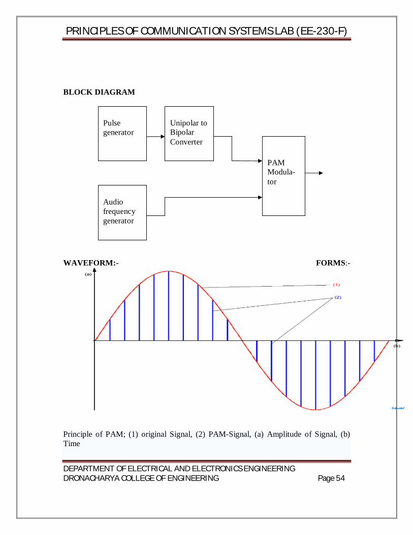
PRINCIPLES OF COMMUNICATION SYSTEMS LAB (EE-230-F)
DEPARTMENT OF ELECTRICAL AND ELECTRONICS ENGINEERING DRONACHARYA COLLEGE OF ENGINEERING Page 54
BLOCK DIAGRAM
WAVEFORM:- FORMS:-
Principle of PAM; (1) original Signal, (2) PAM-Signal, (a) Amplitude of Signal, (b) Time
Pulse generator
Audio frequency generator
Unipolar to Bipolar Converter
PAM Modula- tor
PRINCIPLES OF COMMUNICATION SYSTEMS LAB (EE-230-F)
DEPARTMENT OF ELECTRICAL AND ELECTRONICS ENGINEERING DRONACHARYA COLLEGE OF ENGINEERING Page 55
PROCEDURE:- 1. Make the connection according to the block diagram. 2. Connect pulse generator to the unipolar to bipolar converter 3. Connect the audio frequency of 2 KHz, 2V to modulator. 4. Connect the modulator output to CRO. 5. Observe output on CRO. RESULT:- Pulse modulated waveform is obtained on CRO. PRECAUTIONS:- 1. Do not use open ended wires for connecting to 230 V power supply. 2. Before connecting the power supply plug into socket, ensure power supply should be switched off. 3. Ensure all connections should be tight before switching on the power supply. 4. Take the reading carefully. 5. Power supply should be switched off after completion of experiment. QUIZ / ANSWERS:- Q.1. What is pulse amplitude modulation? Ans. Amplitude of the sampled pulse is varied according to the modulating signal. Q.2. How many types of pulse modulation? Ans. There are two types of PM i.e. PAM and PTM. Q.3. How many types of pulse time modulation? Ans. There are two types of PTM i.e. PWM and PPM. Q.4. What is base band system? Ans. When the basic signal is transmitted without a frequency translation is known as base band signal. Q.5. How many types of pulse amplitude modulation? Ans. There are two types of PAM i.e. single polarity and double polarity. Q.6. Write the demodulation method of Plato sample signal. Ans. (1) using an equalizer (2) using holding circuit. Q.7. Which filter is used in PAM demodulator circuit? Ans. Second order low pass filter. Q.8. Write the two method of multiplexing Ans. (1) FDM (2) TDM Q.9. What is direct method of PTM generation? Ans. In the direct method of PTM generation wave form is generated without generating the PAM. Q.10. What is the merit of flat top sampling? Ans. The tops of pulses are flat thus the pulses have constant amplitude with in the pulse Interval.
PRINCIPLES OF COMMUNICATION SYSTEMS LAB (EE-230-F)
DEPARTMENT OF ELECTRICAL AND ELECTRONICS ENGINEERING DRONACHARYA COLLEGE OF ENGINEERING Page 56
EXPERIMENT 8(b)
AIM:- To study the pulse width modulation. APPARATUS REQUIRED:- CRO, experimental kit, power supply, connecting leads BRIEF THEORY:- PWM is a part of PTM modulation. The PWM is also called PDM (pulse duration modulation) and sometimes it is also called PLM (pulse length modulation).
In PWM width of each pulse depends on the instantaneous value of the base band signal at the sampling instant. In pulse width modulation continuous waveform is sampled at regular intervals and the width of each pulse is kept proportional to the magnitude of signal at that instant in PWM. In pulse width modulation pulse is varied accordance with the modulating signal but the amplitude and starting time of each pulse is fixed .In PWM, the information about the base band signal lies in the trailing edge of the pulse PWM has the disadvantage, when compared with PPM that its pulses are of varying width and therefore of varying power content .This means that transmitter must be powerful enough to handle the maximum- width pulses, although the average power transmitted is perhaps only half of the peak power. PWM still works if synchronization between transmitter and receiver fails. Generation and Demodulation of PWM PWM may be generated by applying trigger pulses to control the duration of these pulses. The emitter coupled mono-stable multi-vibrator is used as voltage to time converter, since its gate width is dependent on the voltage to which the capacitor C is charged .If this voltage is varied in accordance with a signal voltage, a series of rectangular pulses will be obtained, with widths varying as required. The demodulation of pulse width modulation is a simple process. PWM is fed to an integrating circuit from which a signal emerges whose amplitude at any time is proportional to the pulse width at that time. BLOCK DIAGRAM:-
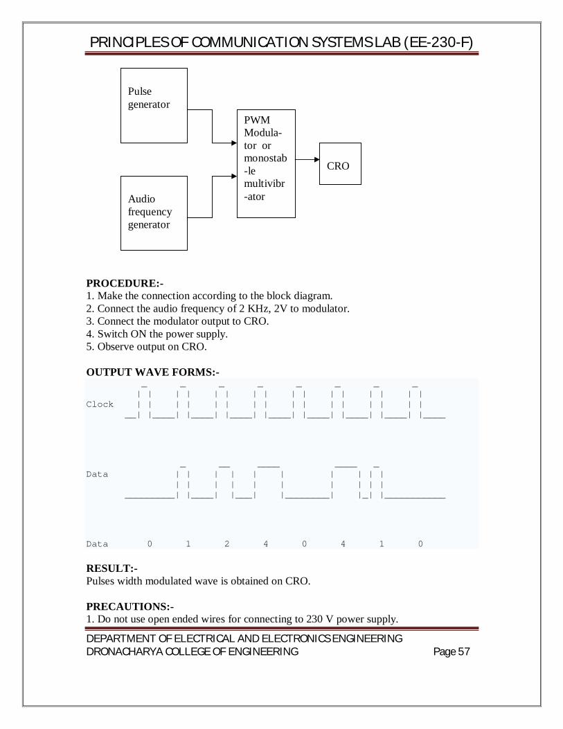
PRINCIPLES OF COMMUNICATION SYSTEMS LAB (EE-230-F)
DEPARTMENT OF ELECTRICAL AND ELECTRONICS ENGINEERING DRONACHARYA COLLEGE OF ENGINEERING Page 57
PROCEDURE:- 1. Make the connection according to the block diagram. 2. Connect the audio frequency of 2 KHz, 2V to modulator. 3. Connect the modulator output to CRO. 4. Switch ON the power supply. 5. Observe output on CRO. OUTPUT WAVE FORMS:- _ _ _ _ _ _ _ _ | | | | | | | | | | | | | | | | Clock | | | | | | | | | | | | | | | | __| |____| |____| |____| |____| |____| |____| |____| |____
_ __ ____ ____ _ Data | | | | | | | | | | | | | | | | | | | | _________| |____| |___| |________| |_| |___________
Data 0 1 2 4 0 4 1 0 RESULT:- Pulses width modulated wave is obtained on CRO. PRECAUTIONS:- 1. Do not use open ended wires for connecting to 230 V power supply.
Pulse generator
Audio frequency generator
PWM Modula- tor or monostab-le multivibr-ator
CRO
PRINCIPLES OF COMMUNICATION SYSTEMS LAB (EE-230-F)
DEPARTMENT OF ELECTRICAL AND ELECTRONICS ENGINEERING DRONACHARYA COLLEGE OF ENGINEERING Page 58
2. Before connecting the power supply plug into socket, ensure power supply should be switched off 3. Ensure all connections should be tight before switching on the power supply. 4. Take the reading carefully. 5. Power supply should be switched off after completion of experiment. QUIZ:- Q.1 Which modulation is PWM? Ans. Analog Modulation Q.2 What are two categories of Pulse Modulation.? Ans.! Analog Modulation 2. Digital Modulation Q.3 What is the unit of signaling speed? Ans. Baud Q.4 What is the disadvantage of PWM? Ans. Due to varying of pulses width power contents of PWM also varying Q.5 Which multivibrator is used for PWM? Ans. Monostable Multivibrator Q.6 Which circuit is used for PWM demodulator? Ans. Integrating circuit. Q.7 What is difference bet. PAM and PWM ? Ans. In PAM, amplitude of pulse is varied according to modulating signal and in PWM,width is varied of pulses. Q.8 How PWM may be generated? Ans. PWM may be generated applying trigger pulses to contol the starting time of pulses from a monostable multivibrator. Q.9 What is the use of sampling theorem? Ans. Sampling Theorem is used to determine minimum sampling speed. Q.10 What is the world wide standard sampling rate? Ans. Eight thousand samples per second.
PRINCIPLES OF COMMUNICATION SYSTEMS LAB (EE-230-F)
DEPARTMENT OF ELECTRICAL AND ELECTRONICS ENGINEERING DRONACHARYA COLLEGE OF ENGINEERING Page 59
EXPERIMENT 8(c) AIM:-To study the pulse position modulation. APPARATUS REQUIRED:- CRO, experimental kit, power supply, connecting leads. THEORY:- In pulse position modulating the amplitude of pulse is kept constant and position of the pulse in relation to the position of the reference pulse or synchronize pulse is varied by each sample value of modulating signal. PPM may be obtained from PWM. In PWM each pulse has a leading edge and a trailing edge but the location of leading edge are fixed where trailing edge are depends on the pulse width. Thus PPM may be obtained from PWM by simply getting side of the leading edger and slots tops of PWM pulses. In pulse position modulating the amplitude of pulse is kept constant and position of the pulse in relation to the position of the reference pulse or synchronize pulse is varied by each sample value of modulating signal. In PWM each pulse has a leading edge and a trailing edge but the location of leading edge are fixed where trailing edge are depends on the pulse width. The trailing edges of PWM pulses are in fact position modulated. Thus PPM may be obtained from PWM by simply getting rid of the leading edge and slots tops of PWM pulses. In comparison with PWM, PPM has the advantage of requiring constant transmitter power output, but the disadvantage of depending on transmitter –receiver synchronization. Generation and demodulation of PPM :
PPM may be generated from PWM easily. First of all, PWM pulses are generated and then they are differentiated. The result is another pulse train which has positive going narrow pulses corresponding to leading edges and negative going narrow pulses corresponding to trailing edges. If the position corresponding to the trailing edges of an un-modulated PWM pulse is counted as zero displacement, then the trailing edges of a modulated pulse will arrive earlier or later. An unmodulated PWM pulse is one that is obtained when the instantaneous signal value is zero. The differentiated pulses corresponding to the leading edges are removed with a diode clipper and the remaining pulses are nothing but position modulated output. When the PPM is demodulated in the receiver, it is again first converted into PWM by using flip-flop or bistable multivibrator. One input of the multivibrator receives trigger pulses from a local generator which is synchronized by trigger pulses received from the transmitter, and these triggers are used to switch off one of the stages of the flip-flop. The PPM pulses are fed to the other base of the flip-flop and switch that stage ON. The period of time during which this particular stage is OFF, depends on the time difference between the two triggers, so that the resulting pulse has a width that depends on the time displacement of each individual PPM pulse. The PWM pulse train thus obtained is a demodulated output.
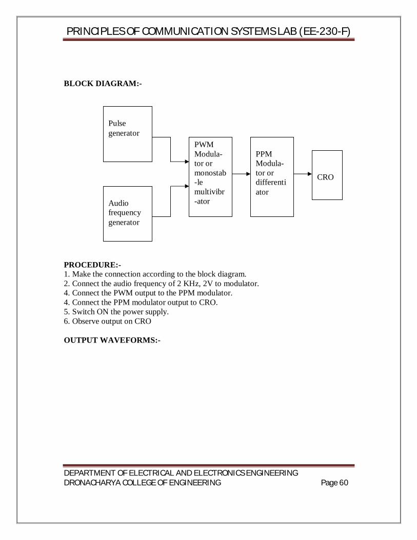
PRINCIPLES OF COMMUNICATION SYSTEMS LAB (EE-230-F)
DEPARTMENT OF ELECTRICAL AND ELECTRONICS ENGINEERING DRONACHARYA COLLEGE OF ENGINEERING Page 60
BLOCK DIAGRAM:-
PROCEDURE:- 1. Make the connection according to the block diagram. 2. Connect the audio frequency of 2 KHz, 2V to modulator. 4. Connect the PWM output to the PPM modulator. 4. Connect the PPM modulator output to CRO. 5. Switch ON the power supply. 6. Observe output on CRO OUTPUT WAVEFORMS:-
Pulse generator
Audio frequency generator
PWM Modula- tor or monostab-le multivibr-ator
PPM Modula- tor or differentiator
CRO
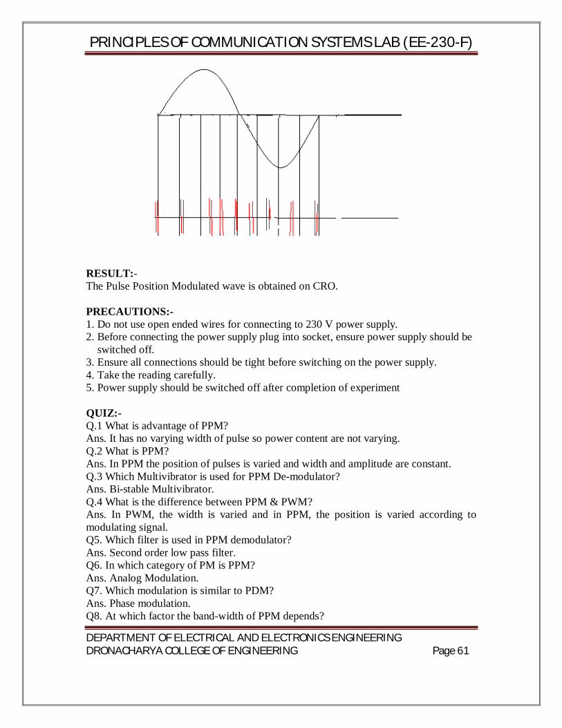
PRINCIPLES OF COMMUNICATION SYSTEMS LAB (EE-230-F)
DEPARTMENT OF ELECTRICAL AND ELECTRONICS ENGINEERING DRONACHARYA COLLEGE OF ENGINEERING Page 61
RESULT:- The Pulse Position Modulated wave is obtained on CRO. PRECAUTIONS:- 1. Do not use open ended wires for connecting to 230 V power supply. 2. Before connecting the power supply plug into socket, ensure power supply should be switched off. 3. Ensure all connections should be tight before switching on the power supply. 4. Take the reading carefully. 5. Power supply should be switched off after completion of experiment QUIZ:- Q.1 What is advantage of PPM? Ans. It has no varying width of pulse so power content are not varying. Q.2 What is PPM? Ans. In PPM the position of pulses is varied and width and amplitude are constant. Q.3 Which Multivibrator is used for PPM De-modulator? Ans. Bi-stable Multivibrator. Q.4 What is the difference between PPM & PWM? Ans. In PWM, the width is varied and in PPM, the position is varied according to modulating signal. Q5. Which filter is used in PPM demodulator? Ans. Second order low pass filter. Q6. In which category of PM is PPM? Ans. Analog Modulation. Q7. Which modulation is similar to PDM? Ans. Phase modulation. Q8. At which factor the band-width of PPM depends?
PRINCIPLES OF COMMUNICATION SYSTEMS LAB (EE-230-F)
DEPARTMENT OF ELECTRICAL AND ELECTRONICS ENGINEERING DRONACHARYA COLLEGE OF ENGINEERING Page 62
Ans. Bandwidth of transmission channel depends on rising time of the pulse.
PRINCIPLES OF COMMUNICATION SYSTEMS LAB (EE-230-F)
DEPARTMENT OF ELECTRICAL AND ELECTRONICS ENGINEERING DRONACHARYA COLLEGE OF ENGINEERING Page 63
EXPERIMENT 9 AIM:-To study Time Division Multiplexing. APPARATUS REQUIRED: (i) C.R.O. (ii) CRO Probe (ii) TDM Pulse Code Modulation Transmitter Trainer (ST 2103) and TDM Pulse Code Modulation Receiver Trainer (ST 2104) (iv) Connecting leads. THEORY:- Time division multiplexing is a technique of transmitting more than one information on the same channel. As can be noticed from the fig. 11 below the samples consists of short pulses followed by another pulse after a long time intervals. This no-activity time intervals can be used to include samples from the other channels as well. This means that several information signals can be transmitted over a single channel by sending samples from different information sources at different moments in time. This technique is known as time division multiplexing or TDM. TDM is widely used in digital communication systems to increase the efficiency of the transmitting medium. TDM can be achieved by electronically switching the samples such that they inter leave sequentially at correct instant in time without mutual interference. The basic 4 channel TDM is shown in fig. 2. The switches S1 & S2 are rotating in the shown direction in a synchronized manner, where S1 is sampling channel to the transmission media. The timing of the two switches is very important to ensure that the samples of one channel are received only by the corresponding channel at the receiver. This synchronization between S1 & S2 must be established by some means for reliable communication. One such method is to send synchronization code (information) along itself to the transmitter all the time. In practice, the switches S1 & S2 are simulated electronically.
Figure 1:Pulse Amplitude Modulated wave with large time Intervals between samples
PRINCIPLES OF COMMUNICATION SYSTEMS LAB (EE-230-F)
DEPARTMENT OF ELECTRICAL AND ELECTRONICS ENGINEERING DRONACHARYA COLLEGE OF ENGINEERING Page 64
On ST2103, the sequence of operation is synchronized to the transmitter clock TX. clock (t.p.3). The time occupied by each clock pulse is called a Bit. The sequence of operation is repeated after every 15 bits. The complete cycle of 15 bits is called as timing frame. The start of the timing frame is denoted by the TX.TO signal (t.p.4) which goes high during the bit time 0. The various bits reserved for the data appearing in the middle of each transmitter clock cycle is shown in fig. The fig.12 shows the complete timing frame .
Figure 2: Principle of 4-Channel TDM System
Bit 0 : This bit is reserved for the synchronization information generated by the Pseudo random sync code generator block More about its operation in the later section. When the Pseudo Random Sync Code is switched OFF a '0' is transmitted. Bit 1 to 7 : These carry a 7 bit data word corresponding to the last sample taken from the analog channel CH.0. Remember that the trainer transmits lowest significant bit (LSB) first. This time interval during which the coded information regarding the analog information is transmitted is called as the timeslot. Since the present timeslot corresponds to channel 0 it is known as timeslot 0. Bit 8 to 14 : This timeslot termed as timeslot 1 contains the 7 bit word corresponding to the last sample taken of analog channel1. As with channel 0 the least significant bit is transmitted first. The receiver requires two signals for its correct operation & reliable communication, namely.
a. Receiver clock operating at the same frequency as that of the ST2103 clock. b. Synchronization signal, which allows the receiver to synchronies its clock/operation with the transmitter’s clock operation. All these requirements can be achieved by transmitting two essential information signals:
I. A Transmit clock signal. II. A Frame synchronization signal.
PRINCIPLES OF COMMUNICATION SYSTEMS LAB (EE-230-F)
DEPARTMENT OF ELECTRICAL AND ELECTRONICS ENGINEERING DRONACHARYA COLLEGE OF ENGINEERING Page 65
The simplest method is to transmit the synchronization information & the clock over a separate transmission link. This results in a simplest receiver. It is used in data communication LAN (Local Area Network) & in telemetry systems. However it is waste of media & is not economical for long distance communications. The ST2103 provides these two signals at TX. clock output (t.p.3) & TX.TO output (t.p.4). In this mode the Pseudo random sync code generator& detector (on ST2104) are switched OFF. The second technique is to transmit the synchronization code along with transmitted data to be sufficiently different from the information samples. The ST2103 involves the use of a pseudo-random sync code generator. These codes are bit streams of '0's & '1's whose occurrence is detected by some rules. The Pseudo - Random Sync Code gets its name from the fact that the occurrence of '0's & '1 's in the stream is random for a portion of sequence i.e. there is equal probability of occurrence of '0' and '1 '. This portion of sequence is 15 bit long on ST2103. On the receiver the pseudo-random sync code detector recognizes the Pseudo random code & use it to identify, which incoming data bit is associated, with which transmitter timeslot The advantage of this technique is that if the synchronization is temporarily lost, due to noise corruption, it can be re-established as the signal clears. Hence there is minimal loss of transmitted information. Also this technique reduces the separate link required for synchronization signal transmission. Mode 1: Mode 1 is TDM system of three transmission links between transmitter & receiver. They are information, TX clock & TX.TO (synchronization) signal links. The Pseudo random sync code generator& Detector are switched OFF in this case. Mode 2: Mode 2 is TDM system of two transmission links between transmitter & receiver. These are information & TX clock signal links. The synchronization is established by sync codes transmitted along with the data stream. No need to say that the pseudo random sync generator & detector are switched ON. Mode 3: Mode 3 is TDM system of one link between transmitter & receiver, namely the link carrying information. Synchronization is again established by the sync codes. The clock signal is regenerated by the phase locked loop (PLL) circuit at the receiver from the transition of the information data bits. BLOCK DIAGRAM:-
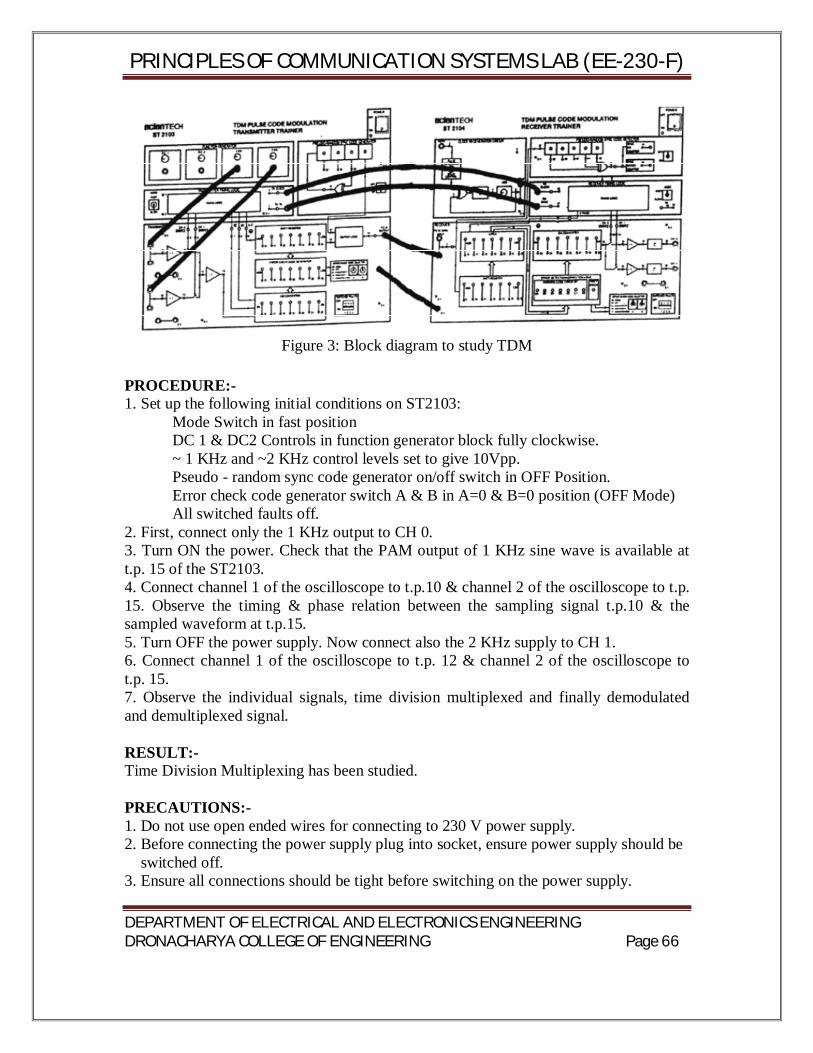
PRINCIPLES OF COMMUNICATION SYSTEMS LAB (EE-230-F)
DEPARTMENT OF ELECTRICAL AND ELECTRONICS ENGINEERING DRONACHARYA COLLEGE OF ENGINEERING Page 66
Figure 3: Block diagram to study TDM
PROCEDURE:- 1. Set up the following initial conditions on ST2103: Mode Switch in fast position DC 1 & DC2 Controls in function generator block fully clockwise. ~ 1 KHz and ~2 KHz control levels set to give 10Vpp. Pseudo - random sync code generator on/off switch in OFF Position. Error check code generator switch A & B in A=0 & B=0 position (OFF Mode) All switched faults off. 2. First, connect only the 1 KHz output to CH 0. 3. Turn ON the power. Check that the PAM output of 1 KHz sine wave is available at t.p. 15 of the ST2103. 4. Connect channel 1 of the oscilloscope to t.p.10 & channel 2 of the oscilloscope to t.p. 15. Observe the timing & phase relation between the sampling signal t.p.10 & the sampled waveform at t.p.15. 5. Turn OFF the power supply. Now connect also the 2 KHz supply to CH 1. 6. Connect channel 1 of the oscilloscope to t.p. 12 & channel 2 of the oscilloscope to t.p. 15. 7. Observe the individual signals, time division multiplexed and finally demodulated and demultiplexed signal. RESULT:- Time Division Multiplexing has been studied. PRECAUTIONS:- 1. Do not use open ended wires for connecting to 230 V power supply. 2. Before connecting the power supply plug into socket, ensure power supply should be switched off. 3. Ensure all connections should be tight before switching on the power supply.
PRINCIPLES OF COMMUNICATION SYSTEMS LAB (EE-230-F)
DEPARTMENT OF ELECTRICAL AND ELECTRONICS ENGINEERING DRONACHARYA COLLEGE OF ENGINEERING Page 67
4. Take the reading carefully. 5. Power supply should be switched off after completion of experiment.
PRINCIPLES OF COMMUNICATION SYSTEMS LAB (EE-230-F)
DEPARTMENT OF ELECTRICAL AND ELECTRONICS ENGINEERING DRONACHARYA COLLEGE OF ENGINEERING Page 68
EXPERIMENT 10 AIM:-To study the pulse code modulation and demodulation with parity and Hamming codes. APPARATUS REQUIRED: (i) C.R.O. (ii) CRO Probe (ii) TDM Pulse Code Modulation Transmitter Trainer (ST 2103) and TDM Pulse Code Modulation Receiver Trainer (ST 2104) (iv) Connecting leads. THEORY:- PCM is a digital process. In this instead of sending a pulse train capable of continuously varying one of the parameters, the PCM generator produces a series of numbers. Each sone of these digits , almost always in binary code, represents the approximate amplitude of the signal sample at that instant . In pulse code modulation, the massage signal is rounded to the nearest of a finite set of allowable values. So that both time and amplitude are discrete form. This allows the massage to be transmitted by means of coded electrical signals. There by distinguishing PCM from all other methods. Modulations with increasing ability of wide band communication channel coupled with the emergence of required device technology. The use of PCM has become a practical reality. The essential operation in the transmitter of PCM system are sampling, quantizing, and encoding. The quantizing and encoding operation are performed in the same circuit called A / D converter. The essential operations in the receiver are regeneration of unpaired signal, decoding and demodulation of train of quantized. Steps in Pulse Code Modulation : Sampling: The analog signal is sampled according to the Nyquist criteria. The nyquist criteria states that for faithful reproduction of the band limited signal, the sampling rate must be at least twice the highest frequency component present in the signal. For audio signals the highest frequency component is 3.4 KHz. So, Sampling Frequency ≥ 2 fm
≥ 2 x 3.4 KHz ≥ 6.8 KHz
Practically, the sampling frequency is kept slightly more than the required rate. In telephony the standard sampling rate is 8 KHz. Sample quantifies the instantaneous value of the analog signal point at sampling point to obtain pulse amplitude output. Allocation of Binary Codes: Each binary word defines a particular narrow range of amplitude level. The sampled value is then approximated to the nearest amplitude level. The sample is then assigned a code corresponding to the amplitude level, which is then transmitted. This process is called as Quantization & it is generally carried out by the A/D converter.
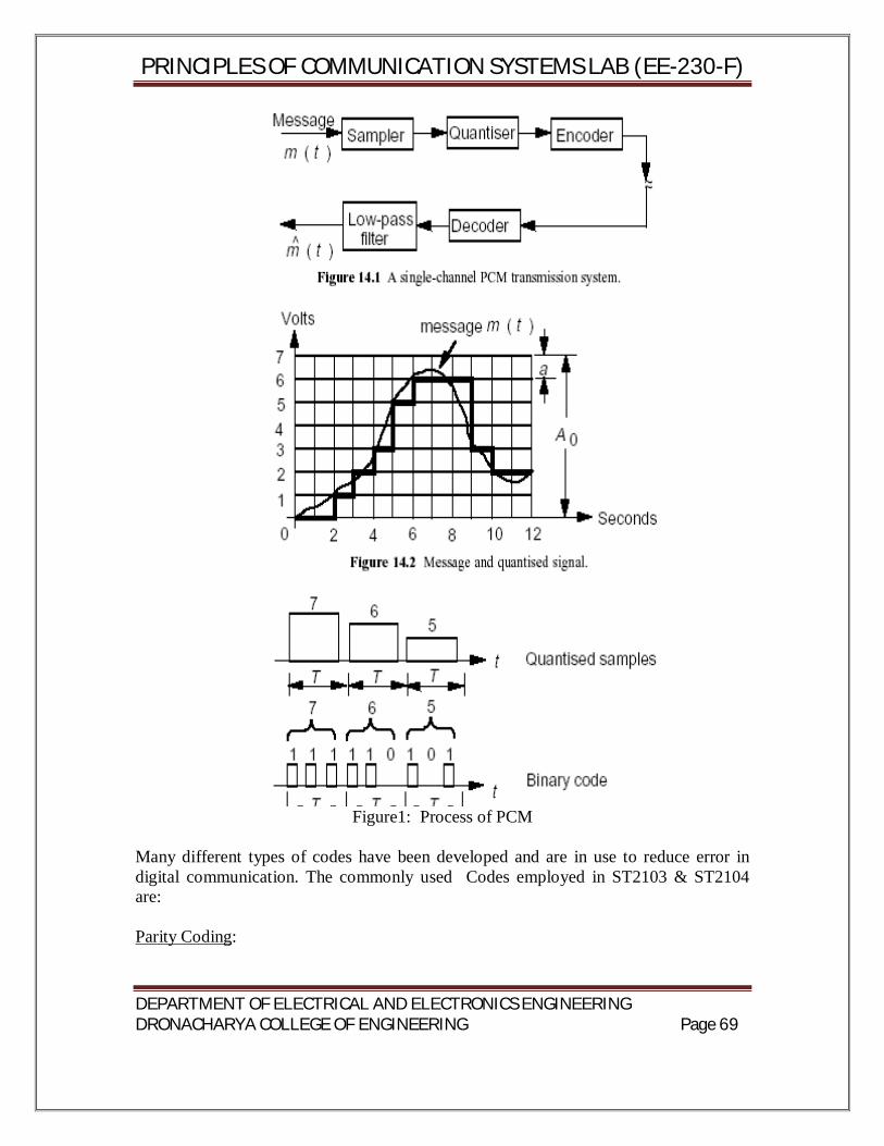
PRINCIPLES OF COMMUNICATION SYSTEMS LAB (EE-230-F)
DEPARTMENT OF ELECTRICAL AND ELECTRONICS ENGINEERING DRONACHARYA COLLEGE OF ENGINEERING Page 69
Figure1: Process of PCM
Many different types of codes have been developed and are in use to reduce error in digital communication. The commonly used Codes employed in ST2103 & ST2104 are: Parity Coding:
PRINCIPLES OF COMMUNICATION SYSTEMS LAB (EE-230-F)
DEPARTMENT OF ELECTRICAL AND ELECTRONICS ENGINEERING DRONACHARYA COLLEGE OF ENGINEERING Page 70
It is the simplest method of error coding. Parity is a method of encoding such that the number of 1's in a codeword is either even or odd Signal parity is established as follows. Each word is examined to determine whether it contains an odd or even number of '1' bits. If even parity is to be established (known as Even parity), a '1' bit is added to each word containing odd '1' and a '0' bit is added to each word containing even '1 'so the result is that all the code words contain an even number of 1 bits after encoding. Similarly, the parity coding can ensure that the total number of '1's in the encoded word is odd. In such number of '1's in the encoded word is odd. In such cases it is called as odd parity. Continuing with the example of even parity, after transmission, each code word is examined to see if it contains an even number of 1 bits. If it does not, the presence of an error is indicated. If it does, the parity bit remains and the data is passed to the user. Note that single bit parity code can detect single errors only and it cannot provide error correction because there is no way of knowing which bit is in error. It is for this reason that parity coding is normally only used on transmission systems where the probability of error occurring is deemed to be low. Hamming Coding: Hamming coding, decode each word at transmitter into a new code by stuffing the word with extra redundant bits. As the name suggests, the redundant bits do not convey information but also provides a method of allowing the receiver to decide when an error has occurred & which bit is in error since the system is binary, the bit in error is easily corrected. Three bit hamming code provides single bit error detection and correction. The ST2103 & ST2104 involves the use of 7 bit word. Therefore only four bits are used for transmitting data if hamming code is selected. The format becomes.
D6 D5 D4 D3 C2 C1 C0 Where C2, C1 & C0 are Hamming Code Bits. Hamming code was invented by R.W. Hamming. It uses three redundant bits, as opposed to the single redundant bit needed by simple parity checking. But it provides a facility of single bit error detection & correction. Code Generation on Trainer The code on this trainer is generated by addicting parity check bit to each group as shown below :
Group 1 D6, D5, D4 Parity Bit - C2 Group 2 D6, D5, D3 Parity Bit - C1 Group 3 D6, D4, D3 Parity Bit – C0
The Groups & Parity bit forms an even parity check group. If an error occurs in any of the digits, the parity is lost & can be detected at receiver e.g. Let us encode binary value
D6, D5, D4, D3 of '1101' Group 1 D6 D5 D4 C2
1 1 0 0 Group 2 D6 D5 D3 C1
1 1 1 1
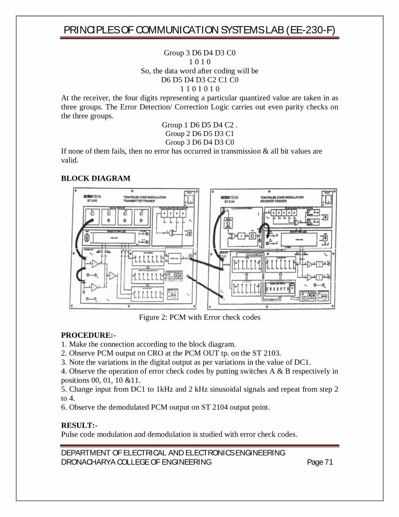
PRINCIPLES OF COMMUNICATION SYSTEMS LAB (EE-230-F)
DEPARTMENT OF ELECTRICAL AND ELECTRONICS ENGINEERING DRONACHARYA COLLEGE OF ENGINEERING Page 71
Group 3 D6 D4 D3 C0 1 0 1 0
So, the data word after coding will be D6 D5 D4 D3 C2 C1 C0
1 1 0 1 0 1 0 At the receiver, the four digits representing a particular quantized value are taken in as three groups. The Error Detection/ Correction Logic carries out even parity checks on the three groups.
Group 1 D6 D5 D4 C2 . Group 2 D6 D5 D3 C1 Group 3 D6 D4 D3 C0
If none of them fails, then no error has occurred in transmission & all bit values are valid. BLOCK DIAGRAM
Figure 2: PCM with Error check codes
PROCEDURE:- 1. Make the connection according to the block diagram. 2. Observe PCM output on CRO at the PCM OUT tp. on the ST 2103. 3. Note the variations in the digital output as per variations in the value of DC1. 4. Observe the operation of error check codes by putting switches A & B respectively in positions 00, 01, 10 &11. 5. Change input from DC1 to 1kHz and 2 kHz sinusoidal signals and repeat from step 2 to 4. 6. Observe the demodulated PCM output on ST 2104 output point. RESULT:- Pulse code modulation and demodulation is studied with error check codes.
PRINCIPLES OF COMMUNICATION SYSTEMS LAB (EE-230-F)
DEPARTMENT OF ELECTRICAL AND ELECTRONICS ENGINEERING DRONACHARYA COLLEGE OF ENGINEERING Page 72
PRECAUTIONS:- 1. Do not use open ended wires for connecting to 230 V power supply. 2. Before connecting the power supply plug into socket, ensure power supply should be switched off. 3. Ensure all connections should be tight before switching on the power supply. 4. Take the reading carefully. 5. Power supply should be switched off after completion of experiment. QUIZ:- Q.1 In which category of PM is PCM? Ans. Digital Modulation Q.2 which noise is occurs in PCM? Ans. Quantization Noise Q.3 what is Quantization? Ans. In PCM, the total amplitude range which is signal may be divided into number of standard level is called quantization. Q.4 which noise is occurs in PCM Ans. Quantization noise. Q.5 How analog signal can be encoded in to bits/ Ans. By delta modulation technique Q.6 what is the advantage of DM over PCM? Ans. DM needs a simple circuit as compared to PCM. Q.7 what is the advantage of PCM? Ans. In PCM, S/N ratio is more than DM Q.8 At which factor bandwidth of PCM depends? Ans. It depends upon the bit duration i.e. sampling period/total no. of bits. Q.9 what is Elastic store? Ans. A device which can store and reproduce data at different speed is Elastic store. Q.10 Write down one example of Elastic store. Ans. Tape-recorder.
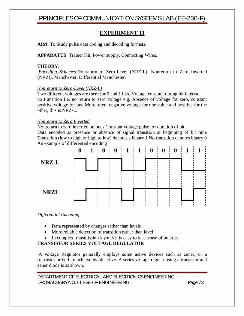
PRINCIPLES OF COMMUNICATION SYSTEMS LAB (EE-230-F)
DEPARTMENT OF ELECTRICAL AND ELECTRONICS ENGINEERING DRONACHARYA COLLEGE OF ENGINEERING Page 73
EXPERIMENT 11 AIM: To Study pulse data coding and decoding formats. APPARATUS: Trainer Kit, Power supply, Connecting Wires. THEORY: Encoding Schemes:Nonreturn to Zero-Level (NRZ-L), Nonreturn to Zero Inverted (NRZI), Manchester, Differential Manchester. Nonreturn to Zero-Level (NRZ-L) Two different voltages are there for 0 and 1 bits. Voltage constant during bit interval no transition I.e. no return to zero voltage e.g. Absence of voltage for zero, constant positive voltage for one More often, negative voltage for one value and positive for the other, this is NRZ-L. Nonreturn to Zero Inverted Nonreturn to zero inverted on ones Constant voltage pulse for duration of bit Data encoded as presence or absence of signal transition at beginning of bit time Transition (low to high or high to low) denotes a binary 1 No transition denotes binary 0 An example of differential encoding
Differential Encoding
Data represented by changes rather than levels More reliable detection of transition rather than level In complex transmission layouts it is easy to lose sense of polarity
TRANSISTOR SERIES VOLTAGE REGULATOR A voltage Regulator generally employs some active devices such as zener, or a transistor or both to achieve its objective. A series voltage regular using a transistor and zener diode is as shown,
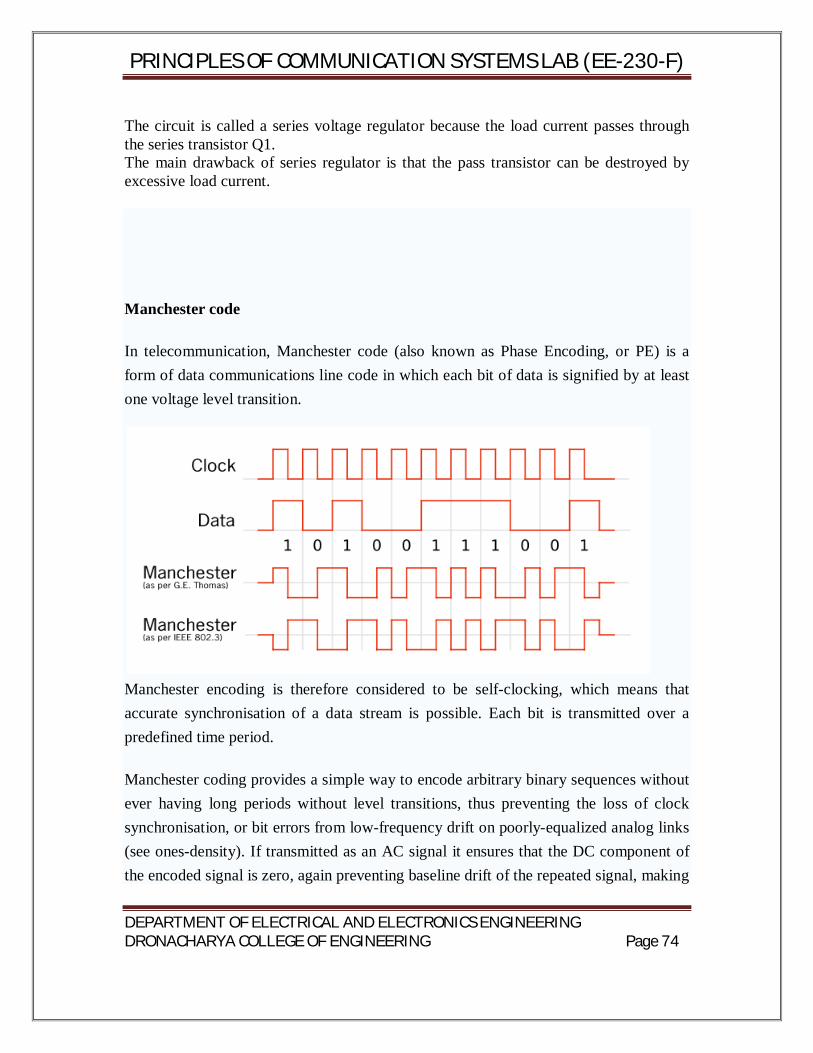
PRINCIPLES OF COMMUNICATION SYSTEMS LAB (EE-230-F)
DEPARTMENT OF ELECTRICAL AND ELECTRONICS ENGINEERING DRONACHARYA COLLEGE OF ENGINEERING Page 74
The circuit is called a series voltage regulator because the load current passes through the series transistor Q1. The main drawback of series regulator is that the pass transistor can be destroyed by excessive load current.
Manchester code
In telecommunication, Manchester code (also known as Phase Encoding, or PE) is a form of data communications line code in which each bit of data is signified by at least one voltage level transition.
Manchester encoding is therefore considered to be self-clocking, which means that accurate synchronisation of a data stream is possible. Each bit is transmitted over a predefined time period.
Manchester coding provides a simple way to encode arbitrary binary sequences without ever having long periods without level transitions, thus preventing the loss of clock synchronisation, or bit errors from low-frequency drift on poorly-equalized analog links (see ones-density). If transmitted as an AC signal it ensures that the DC component of the encoded signal is zero, again preventing baseline drift of the repeated signal, making
PRINCIPLES OF COMMUNICATION SYSTEMS LAB (EE-230-F)
DEPARTMENT OF ELECTRICAL AND ELECTRONICS ENGINEERING DRONACHARYA COLLEGE OF ENGINEERING Page 75
it easy to regenerate and preventing waste of energy. However, there are today many more sophisticated codes (8B/10B encoding) which accomplish the same aims with less bandwidth overhead, and less synchronisation ambiguity in pathological cases. Regardless of these losses, Manchester coding has been adopted into many efficient and widely used telecommunications standards, such as Ethernet.
An example of Manchester encoding showing both conventions PROCEDURE:
1 Make the connection according to the block diagram. Power supply should be Switched off .
2 Connect frequency-modulated output to the AM De-Modulator input. connections should be tight.
3 Connect the De-Modulator output to CRO. 4 Observe output on CRO. Take output carefully.
RESULT: Different pulse data coding and decoding formats have been studied. PRECAUTIONS:- 1. Do not use open ended wires for connecting to 230 V power supply. 2. Before connecting the power supply plug into socket, ensure power supply should be switched off 3. Ensure all connections should be tight before switching on the power supply. 4. Take the reading carefully. 5. Power supply should be switched off after completion
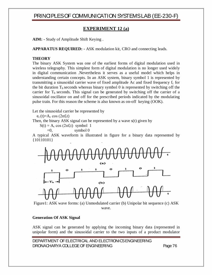
PRINCIPLES OF COMMUNICATION SYSTEMS LAB (EE-230-F)
DEPARTMENT OF ELECTRICAL AND ELECTRONICS ENGINEERING DRONACHARYA COLLEGE OF ENGINEERING Page 76
EXPERIMENT 12 (a)
AIM: - Study of Amplitude Shift Keying . APPARATUS REQUIRED: - ASK modulation kit, CRO and connecting leads. THEORY The binary ASK System was one of the earliest forms of digital modulation used in wireless telegraphy. This simplest form of digital modulation is no longer used widely in digital communication .Nevertheless it serves as a useful model which helps in understanding certain concepts. In an ASK system, binary symbol 1 is represented by transmitting a sinusoidal carrier wave of fixed amplitude Ac and fixed frequency fc for the bit duration Tb seconds whereas binary symbol 0 is represented by switching off the carrier for Tb seconds. This signal can be generated by switching off the carrier of a sinusoidal oscillator on and off for the prescribed periods indicated by the modulating pulse train. For this reason the scheme is also known as on-off keying (OOK). Let the sinusoidal carrier be represented by ec (t)=Ac cos (2пfct) Then, the binary ASK signal can be represented by a wave s(t) given by S(t) = Ac cos (2пfct) symbol 1 =0, symbol 0 A typical ASK waveform is illustrated in figure for a binary data represented by {10110101}
Figure1: ASK wave forms: (a) Unmodulated carrier (b) Unipolar bit sequence (c) ASK
wave. Generation Of ASK Signal ASK signal can be generated by applying the incoming binary data (represented in unipolar form) and the sinusoidal carrier to the two inputs of a product modulator
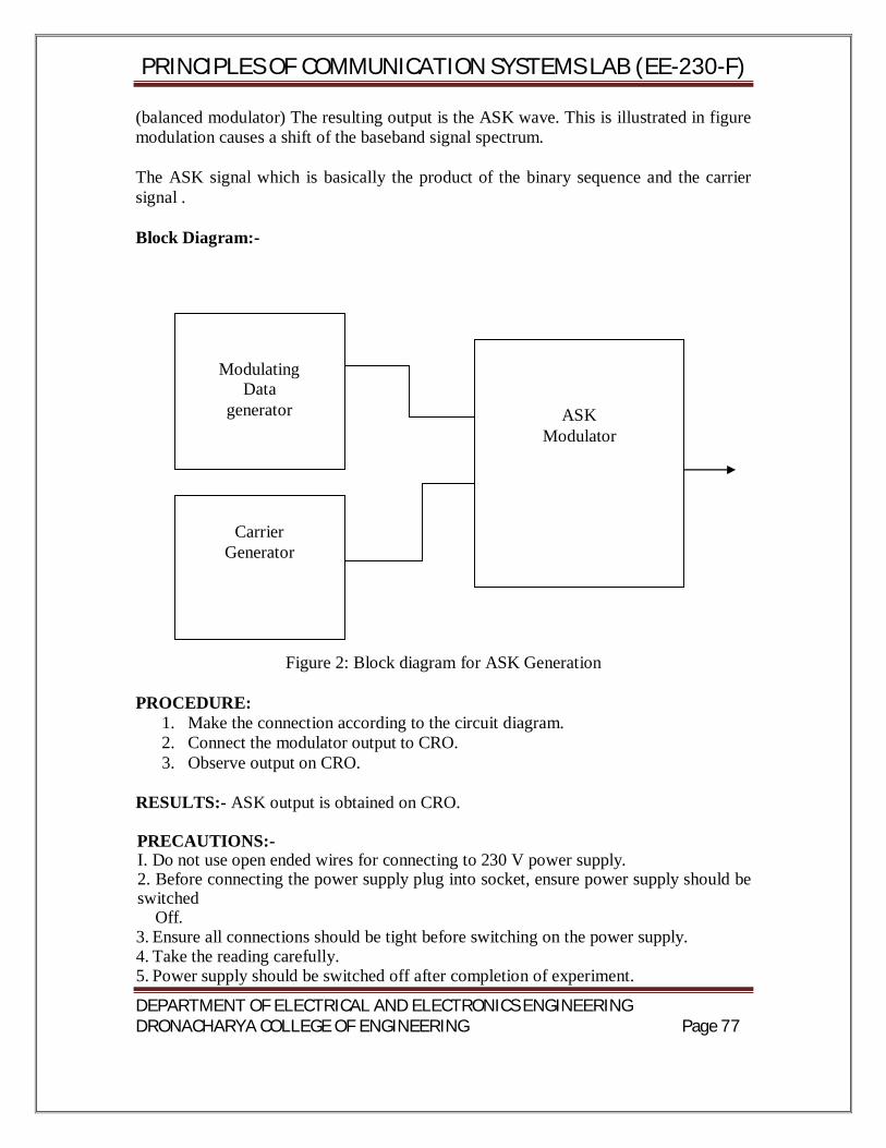
PRINCIPLES OF COMMUNICATION SYSTEMS LAB (EE-230-F)
DEPARTMENT OF ELECTRICAL AND ELECTRONICS ENGINEERING DRONACHARYA COLLEGE OF ENGINEERING Page 77
(balanced modulator) The resulting output is the ASK wave. This is illustrated in figure modulation causes a shift of the baseband signal spectrum. The ASK signal which is basically the product of the binary sequence and the carrier signal . Block Diagram:-
Figure 2: Block diagram for ASK Generation
PROCEDURE:
1. Make the connection according to the circuit diagram. 2. Connect the modulator output to CRO. 3. Observe output on CRO.
RESULTS:- ASK output is obtained on CRO.
PRECAUTIONS:- I. Do not use open ended wires for connecting to 230 V power supply. 2. Before connecting the power supply plug into socket, ensure power supply should be switched Off. 3. Ensure all connections should be tight before switching on the power supply. 4. Take the reading carefully. 5. Power supply should be switched off after completion of experiment.
Modulating Data
generator
Carrier
Generator
ASK
Modulator
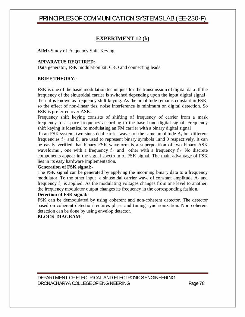
PRINCIPLES OF COMMUNICATION SYSTEMS LAB (EE-230-F)
DEPARTMENT OF ELECTRICAL AND ELECTRONICS ENGINEERING DRONACHARYA COLLEGE OF ENGINEERING Page 78
EXPERIMENT 12 (b)
AIM:-Study of Frequency Shift Keying. APPARATUS REQUIRED:- Data generator, FSK modulation kit, CRO and connecting leads. BRIEF THEORY:- FSK is one of the basic modulation techniques for the transmission of digital data .If the frequency of the sinusoidal carrier is switched depending upon the input digital signal , then it is known as frequency shift keying. As the amplitude remains constant in FSK, so the effect of non-linear ties, noise interference is minimum on digital detection. So FSK is preferred over ASK. Frequency shift keying consists of shifting of frequency of carrier from a mask frequency to a space frequency according to the base band digital signal. Frequency shift keying is identical to modulating an FM carrier with a binary digital signal In an FSK system, two sinusoidal carrier waves of the same amplitude Ac but different frequencies fc1 and fc2 are used to represent binary symbols 1and 0 respectively. It can be easily verified that binary FSK waveform is a superposition of two binary ASK waveforms , one with a frequency fc1 and other with a frequency fc2. No discrete components appear in the signal spectrum of FSK signal. The main advantage of FSK lies in its easy hardware implementation. Generation of FSK signal:- The PSK signal can be generated by applying the incoming binary data to a frequency modulator. To the other input a sinusoidal carrier wave of constant amplitude Ac and frequency fc is applied. As the modulating voltages changes from one level to another, the frequency modulator output changes its frequency in the corresponding fashion. Detection of FSK signal:- FSK can be demodulated by using coherent and non-coherent detector. The detector based on coherent detection requires phase and timing synchronization. Non coherent detection can be done by using envelop detector. BLOCK DIAGRAM:-
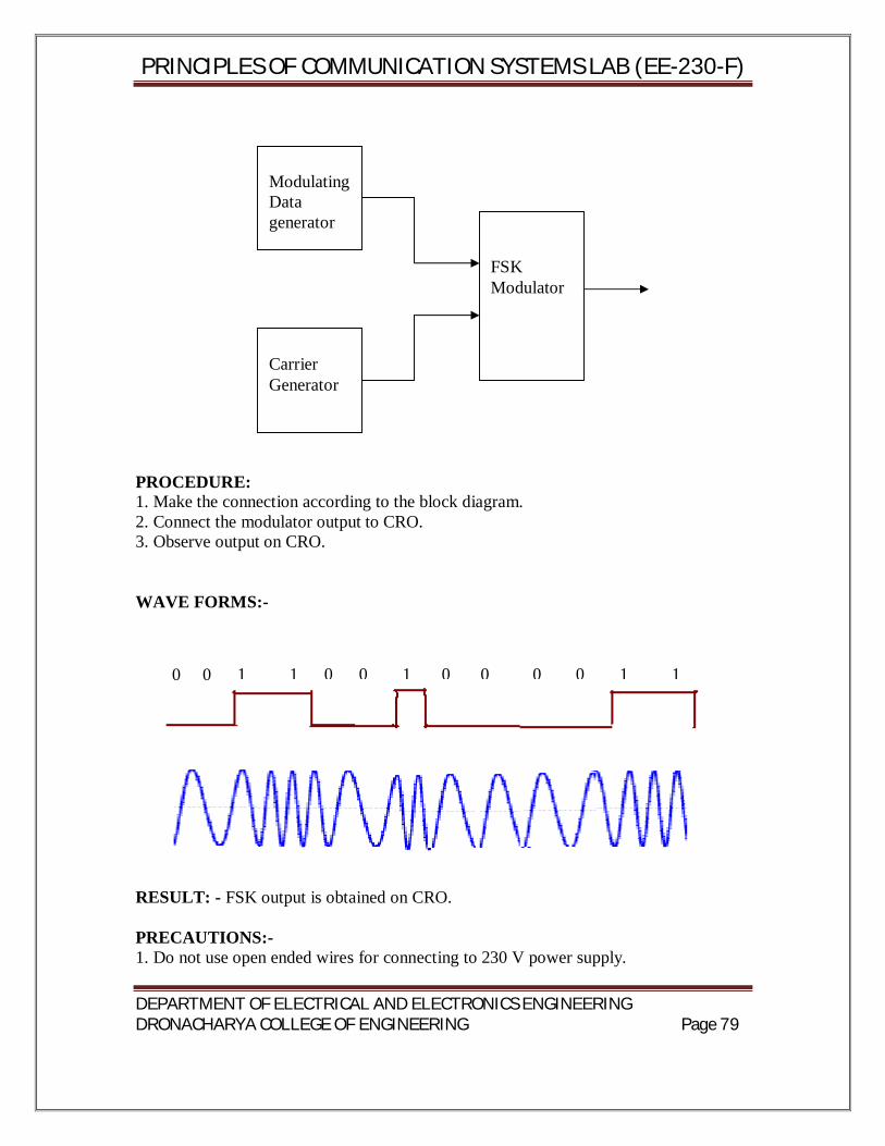
PRINCIPLES OF COMMUNICATION SYSTEMS LAB (EE-230-F)
DEPARTMENT OF ELECTRICAL AND ELECTRONICS ENGINEERING DRONACHARYA COLLEGE OF ENGINEERING Page 79
PROCEDURE: 1. Make the connection according to the block diagram. 2. Connect the modulator output to CRO. 3. Observe output on CRO. WAVE FORMS:-
RESULT: - FSK output is obtained on CRO. PRECAUTIONS:- 1. Do not use open ended wires for connecting to 230 V power supply.
Modulating Data generator
Carrier Generator
FSK Modulator
0 0 1 1 0 0 1 0 0 0 0 1 1
PRINCIPLES OF COMMUNICATION SYSTEMS LAB (EE-230-F)
DEPARTMENT OF ELECTRICAL AND ELECTRONICS ENGINEERING DRONACHARYA COLLEGE OF ENGINEERING Page 80
2. Before connecting the power supply plug into socket, ensure power supply should be switched off 3. Ensure all connections should be tight before switching on the power supply. 4. Take the reading carefully. 5. Power supply should be switched off after completion of experiment QUIZ:- Q.1 What is FSK? Ans. This is one of the basic modulation techniques for transmission of digital data.
The frequency of carrier is switched on or off according to the input digital signal.
Q.2 Why FSK is preferred over ASK? Ans. Because of constant amplitude of FSK the effect of non-linearity’s and noise interference is minimum on signal detection. Q.3 what are various components of FSK detector? Ans. Two synchronous detector, differential amplifier, low-pass filter. Q.4 What is BFSK? Ans . In BFSK frequency of the carrier is sifted according to the binary symbol
keeping the phase of the carrier unaffected. Q.5 What is the difference between FM and FSK? Ans. FM is a analog modulation technique where FSK is digital modulation technique. Q6. How BFSK signal is generated? Ans. An input signal is processed in two paths each existing of level shifter and
product modulator. One path uses directly and other path uses inverter signal.Orthogonal carrier signal are used as the other input for the product modulator. The output of the product modulator are added which generates a BFSK.
Q.7 What is the bandwidth of BFSK? Ans. 4fb where fb - bandwidth of the input signal. Q.8 Compare bandwidth of BFSK and BPSK. Ans. Bandwidth of BFSK= 2(bandwidth of BPSK) Q.9 What is the disadvantage of BFSK? Ans. The error rate of BFSK is more as compared to BPSK. Q.10 How can you detect FSK by non-coherent method? Ans. BFSK waves may be demodulated coherently using envelop detectors.
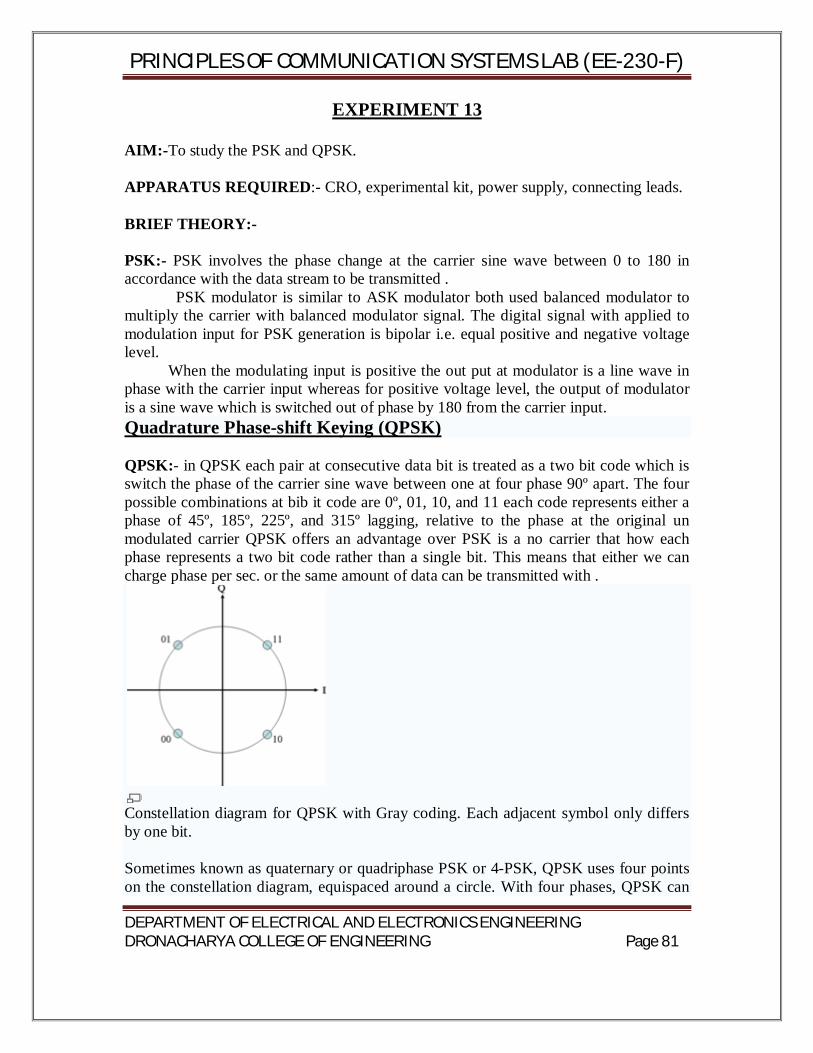
PRINCIPLES OF COMMUNICATION SYSTEMS LAB (EE-230-F)
DEPARTMENT OF ELECTRICAL AND ELECTRONICS ENGINEERING DRONACHARYA COLLEGE OF ENGINEERING Page 81
EXPERIMENT 13
AIM:-To study the PSK and QPSK. APPARATUS REQUIRED:- CRO, experimental kit, power supply, connecting leads. BRIEF THEORY:- PSK:- PSK involves the phase change at the carrier sine wave between 0 to 180 in accordance with the data stream to be transmitted . PSK modulator is similar to ASK modulator both used balanced modulator to multiply the carrier with balanced modulator signal. The digital signal with applied to modulation input for PSK generation is bipolar i.e. equal positive and negative voltage level. When the modulating input is positive the out put at modulator is a line wave in phase with the carrier input whereas for positive voltage level, the output of modulator is a sine wave which is switched out of phase by 180 from the carrier input. Quadrature Phase-shift Keying (QPSK) QPSK:- in QPSK each pair at consecutive data bit is treated as a two bit code which is switch the phase of the carrier sine wave between one at four phase 90º apart. The four possible combinations at bib it code are 0º, 01, 10, and 11 each code represents either a phase of 45º, 185º, 225º, and 315º lagging, relative to the phase at the original un modulated carrier QPSK offers an advantage over PSK is a no carrier that how each phase represents a two bit code rather than a single bit. This means that either we can charge phase per sec. or the same amount of data can be transmitted with .
Constellation diagram for QPSK with Gray coding. Each adjacent symbol only differs by one bit.
Sometimes known as quaternary or quadriphase PSK or 4-PSK, QPSK uses four points on the constellation diagram, equispaced around a circle. With four phases, QPSK can
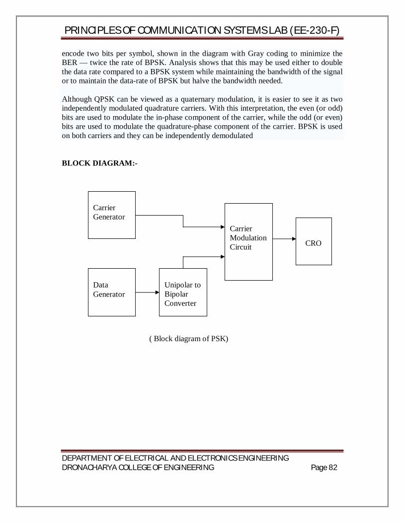
PRINCIPLES OF COMMUNICATION SYSTEMS LAB (EE-230-F)
DEPARTMENT OF ELECTRICAL AND ELECTRONICS ENGINEERING DRONACHARYA COLLEGE OF ENGINEERING Page 82
encode two bits per symbol, shown in the diagram with Gray coding to minimize the BER — twice the rate of BPSK. Analysis shows that this may be used either to double the data rate compared to a BPSK system while maintaining the bandwidth of the signal or to maintain the data-rate of BPSK but halve the bandwidth needed.
Although QPSK can be viewed as a quaternary modulation, it is easier to see it as two independently modulated quadrature carriers. With this interpretation, the even (or odd) bits are used to modulate the in-phase component of the carrier, while the odd (or even) bits are used to modulate the quadrature-phase component of the carrier. BPSK is used on both carriers and they can be independently demodulated
BLOCK DIAGRAM:-
( Block diagram of PSK)
Carrier Generator
Data Generator
Carrier Modulation Circuit
Unipolar to Bipolar Converter
CRO
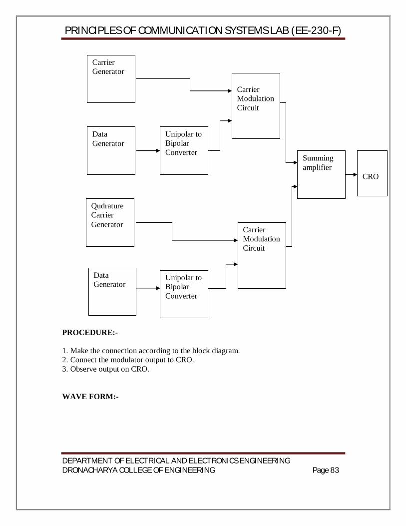
PRINCIPLES OF COMMUNICATION SYSTEMS LAB (EE-230-F)
DEPARTMENT OF ELECTRICAL AND ELECTRONICS ENGINEERING DRONACHARYA COLLEGE OF ENGINEERING Page 83
PROCEDURE:- 1. Make the connection according to the block diagram. 2. Connect the modulator output to CRO. 3. Observe output on CRO. WAVE FORM:-
Carrier Generator
Data Generator
Qudrature Carrier Generator
Data Generator
Unipolar to Bipolar Converter
Carrier Modulation Circuit
Summing amplifier
Unipolar to Bipolar Converter
Carrier Modulation Circuit
CRO
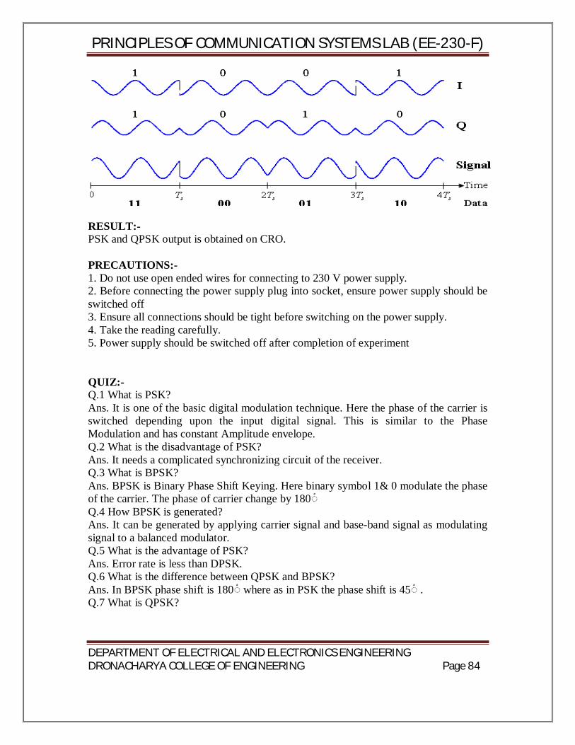
PRINCIPLES OF COMMUNICATION SYSTEMS LAB (EE-230-F)
DEPARTMENT OF ELECTRICAL AND ELECTRONICS ENGINEERING DRONACHARYA COLLEGE OF ENGINEERING Page 84
RESULT:- PSK and QPSK output is obtained on CRO. PRECAUTIONS:- 1. Do not use open ended wires for connecting to 230 V power supply. 2. Before connecting the power supply plug into socket, ensure power supply should be switched off 3. Ensure all connections should be tight before switching on the power supply. 4. Take the reading carefully. 5. Power supply should be switched off after completion of experiment QUIZ:- Q.1 What is PSK? Ans. It is one of the basic digital modulation technique. Here the phase of the carrier is switched depending upon the input digital signal. This is similar to the Phase Modulation and has constant Amplitude envelope. Q.2 What is the disadvantage of PSK? Ans. It needs a complicated synchronizing circuit of the receiver. Q.3 What is BPSK? Ans. BPSK is Binary Phase Shift Keying. Here binary symbol 1& 0 modulate the phase of the carrier. The phase of carrier change by 180 ْ◌ Q.4 How BPSK is generated? Ans. It can be generated by applying carrier signal and base-band signal as modulating signal to a balanced modulator. Q.5 What is the advantage of PSK? Ans. Error rate is less than DPSK. Q.6 What is the difference between QPSK and BPSK? Ans. In BPSK phase shift is 180 ْ◌ where as in PSK the phase shift is 45 ْ◌ . Q.7 What is QPSK?
PRINCIPLES OF COMMUNICATION SYSTEMS LAB (EE-230-F)
DEPARTMENT OF ELECTRICAL AND ELECTRONICS ENGINEERING DRONACHARYA COLLEGE OF ENGINEERING Page 85
Ans. In QPSK two successive bits are combined. This combination of two bits forms four distinguishing symbols. When the symbol is changed to next symbol the phase of carrier is changed by 45 ْ◌ . Q.8 How QPSK is generated? Ans. The input binary sequence is first converted to a bipolar NRZ type of signal called b(t) than it is divided by demultipluxer and added together after insertion of carrier. The generates QPSK signal. Q.9 How QPSK is detected? Ans. Basically QPSK receiver uses a synchronous reception. A coherent carrier applied to the two synchronous demodulator, each consists of a multiplier and an integrator. The output is detected original signal. Q.10 What is DPSK? Ans. DPSK is differential phase shift keying and is a non-coherent versus of PSK.DPSK does not need a coherent carrier at the demodulator. The input sequence of binary bits is modified such that the next bit depends upon the previous bit.
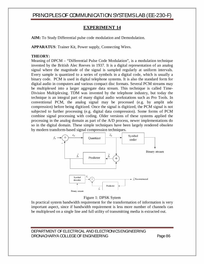
PRINCIPLES OF COMMUNICATION SYSTEMS LAB (EE-230-F)
DEPARTMENT OF ELECTRICAL AND ELECTRONICS ENGINEERING DRONACHARYA COLLEGE OF ENGINEERING Page 86
EXPERIMENT 14
AIM: To Study Differential pulse code modulation and Demodulation. APPARATUS: Trainer Kit, Power supply, Connecting Wires. THEORY: Meaning of DPCM – “Differential Pulse Code Modulation”, is a modulation technique invented by the British Alec Reeves in 1937. It is a digital representation of an analog signal where the magnitude of the signal is sampled regularly at uniform intervals. Every sample is quantized to a series of symbols in a digital code, which is usually a binary code. PCM is used in digital telephone systems. It is also the standard form for digital audio in computers and various compact disc formats. Several PCM streams may be multiplexed into a larger aggregate data stream. This technique is called Time-Division Multiplexing. TDM was invented by the telephone industry, but today the technique is an integral part of many digital audio workstations such as Pro Tools. In conventional PCM, the analog signal may be processed (e.g. by amplit ude compression) before being digitized. Once the signal is digitized, the PCM signal is not subjected to further processing (e.g. digital data compression). Some forms of PCM combine signal processing with coding. Older versions of these systems applied the processing in the analog domain as part of the A/D process, newer implementations do so in the digital domain. These simple techniques have been largely rendered obsolete by modern transform-based signal compression techniques.
Figure 1: DPSK Sytem
In practical system bandwidth requirement for the transformation of information is very important aspect, since if bandwidth requirement is less more number of channels can be multiplexed on a single line and full utility of transmitting media is extracted out.
PRINCIPLES OF COMMUNICATION SYSTEMS LAB (EE-230-F)
DEPARTMENT OF ELECTRICAL AND ELECTRONICS ENGINEERING DRONACHARYA COLLEGE OF ENGINEERING Page 87
In a system in which a baseband signal m(t) is transmitted by sampling, there is available a scheme of transmission which is an alternative to transmitting the sample values at each sampling time . We can instead, at each sampling time, say the Kth
sampling time, transmit the difference between the sample value m(k) at sampling time K and the sample value m(K-1) at time k-1. If such changes are transmitted, then simply by adding up these changes we shall generate at the receiver a waveform identical in form to m (t). PROCEDURE:
1. Make the connection according to the circuit diagram. 2. Observe output on CRO.
RESULTS:- DPSK modulation and demodulation has been studied.
PRECAUTIONS:- 1. Do not use open ended wires for connecting to 230 V power supply. 2. Before connecting the power supply plug into socket, ensure power supply should be switched off 3. Ensure all connections should be tight before switching on the power supply. 4. Take the reading carefully. 5. Power supply should be switched off after completion of experiment


![Principles of Communication - VTU Solutionvtusolution.in/.../principles_of_communication_systems_[15ec45].pdf · vtusolution.in Principles of Communication • The communication process:](https://img.pdfslide.net/doc/110x75/5b62e7027f8b9a3c5e8b59db/principles-of-communication-vtu-15ec45pdf-vtusolutionin-principles-of-communication.jpg)