Embed Size (px)
Citation preview

류 대 우 [email protected]
EMC 적합성을위한PCB설계기술
Printed Circuit board Design Techniques for EMC Compliance
2007. 7. 14.

류 대 우 [email protected]
1. Introduction.2. 인쇄회로기판기초.3. Bypassing and Decoupling.4. 클럭회로.5. 정전기방전보호.6. 추가적인설계기술.7. Noise의최소화방법.
목차

류 대 우 [email protected]
Noise의발생원인
• The three primary means of noise coupling
1. Conductive coupling
2. Common impedance coupling.
3. Coupling by radiated electromagnetic fields.
1. Introduction

류 대 우 [email protected]
• 신호의카테고리를분류한다.
• VLSI 회로의소자밀도를고려한다.
• 임피던스매칭을한다.
• Line의경로설정(Routing)
• PCB의층적층의할당.
PCB 설계시유의사항
류 대 우 [email protected]
• Microstrip
GroundPlane Dielectric
Signal Trace
Stripline보다빠른클럭, 논리신호의전달
• StriplineReference
Plane
Signal Trace
Signal Delay가문제되나, RF복사를억제
2. 인쇄회로기판기초

류 대 우 [email protected]
Layer # 1 2 3 4 5 6 7 8 9 10 Comments
2 S1 S2 Lower-speed designs4 S1 G P S2 6 S1 G S2 S3 P S4 Lower-speed designs 6 S1 S2 G P S3 S4 Default critical signals to S2 only6 S1 G S2 P G S3 Default lower-speed to S2-S38 S1 S2 G S3 S4 P S5 S6 Default high-speed to S2-S38 S1 G S2 G P S3 G S4 Best for EMC
S : Signal Layer, P : Power, G : Ground
층 적층 할당

류 대 우 [email protected]
1. 두층기판위에 Power와 Ground Line을근접시킨다.
2. Ground Plane 보다 물리적으로 더 작게Power Plane을만든다. (20-H Rule)
Power Plane
Ground Plane
Trace
Power Plane
Ground Plane
RF emission occur RF emission do not occur
Fringing Effect
H
20H
H
20-H 규칙

류 대 우 [email protected]
1. 단일점접지.
• 1 MHz 이하의클럭율을이용한저주파시스템에응용.•오디오, 아날로그기구, 60Hz 전력시스템에사용.
2. 다중점접지.
• 10 MHz 이상의클럭율을이용한고주파시스템에사용.

류 대 우 [email protected]
1. Decoupling Capacitor Placement.Decoupling Capator는가능한 IC와가깝게해야한다.
VCC
GNDD.C.
2. Unused Inputs.Unused Inputs는일반적으로직렬저항과함께 VCC 또는Ground에연결되어야한다.
3. Bypassing and Decoupling

류 대 우 [email protected]
1. 가능한가깝게모든전력과접지 Trace를유지한다.
2. Ground에가능한근접하게 Signal Line을유지한다.
3. Line 의길이를짧게한다.
4. 가능한많은접지평면을가지고기판의이용되지않는영역을채운다.
5. I/O 커넥터에근접하게논리소자와필터소자를위치시킨다.
접지루프의최소화.

류 대 우 [email protected]
•클럭발생기, 관련소자, 분배선은 PCB에서 RF 방출의원인이된다.
• Clock Trace는예외없이, 나머지 Trace를자동경로설정하기이전에수동으로경로가지정되어야한다.
frtm a x =
×1
πf m ax = 발생된최대 RF 주파수
rt = Pulse or Edge Rise Time
4. 클럭회로(Clock Circuits)

류 대 우 [email protected]
하나의 Localized Ground Plane 전체에발진기, 크리스탈그리고클럭을지원하는회로(Buffer, Driver)를위치시킨다.LGP는 PCB의맨위에위치하고, 최소두개의여분Bias와발진기접지핀모두를통해서 PCB의주요접지평판으로직접연결된다.
OSC ClockDriver
LGPVias to the groundplane in addition tothe ground pins ofthe devices.
Localized Ground Plane (LGP)

류 대 우 [email protected]
• Clock에서실제 RF 복사가문제가되는것은 Clock의 Frequency가아니라 Clock Signal의 Edge Rate이다.(V=L di/dt, I=C dv/dt에서 di & dt의문제이다.)
•스위칭속도가높아지면클럭드라이브로부터직렬종단저항기가 Trace임피던스 Z0와같아야하는점이중요해진다.
•클럭 Trace의길이가최고주파수의 λ/20 보다작게설계한다.

류 대 우 [email protected]
•보호 Trace와병렬 Trace의사용
a. 3-W 규칙의강화.b. High-Threat 신호 Trace에서다른회로 Trace까지
Common Mode RF결합을막음.c. 회귀경로의낮은임피던스제공.

류 대 우 [email protected]
a. 신호 Trace가길면접지평판에다중으로연결한다.b. 단지짧은거리에한해서공통보호 Trace가공유될수있다.
Via to the ground planeor device grounds.
Clock trace on a plane withvia to another plane
Guard trace
Clock trace
보호 Trace의사용
류 대 우 [email protected]
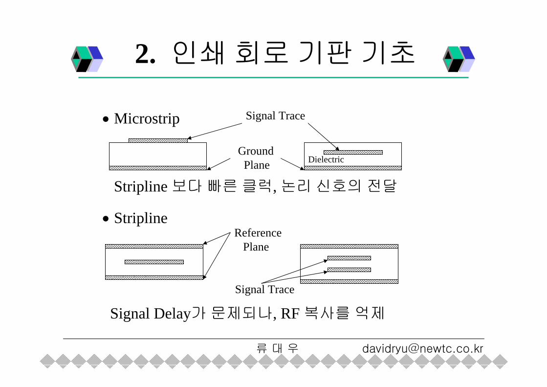
.5가지공통종단방법
a. 직렬종단저항. (적은 dc 잡음Margin)b. 병렬종단저항. (전력소비가크다)c. Thevenin 망. (CMOS용고전력) d. RC망.e. 다이오드망. (Undershoot 제한)
=
||
|
|a b
c d e
Trace Termination

류 대 우 [email protected]
Osillator
Buffer
ASIC
I/O Controller
CacheOptimal Trace Routing for Clock Signals with Electrically Short Traces
Osillator
Buffer
ASIC
I/O Controller
Cache
Optimal Trace Routing for Clock Signals with Electrically Long Traces with respect to Clock Period
Osillator
Buffer
ASIC
I/O Controller
Cache
//=
o +V
Poor Trace Routing for Clock Signals.

류 대 우 [email protected]
3-W 규칙Trace 간의이격거리는반드시중앙선로에서중앙선로까지측정된 Trace 폭에대해세배가 되어야함: 논리전류에대략 70%의선속한계를나타냄.
w w w w w w
via
ww
3W 3W
Trace 분리와 3-W 규칙

류 대 우 [email protected]
I/O Connector
Controller
Via to ground plane
Triangle connected tosignal trace
a. 스파크갭.
b. LC 필터.고주파수 ESD 에너지를시스템에들어오지못하게하는저역통과 LC 필터를구성한다.
C. 고전압커패시터
0.01” distance spacingbetween triangles
5. 정전기방전보호

류 대 우 [email protected]
Device+5V
gnd
+5Vgnd Device
Signal Trace
Device+5V
gnd
+5Vgnd Device
Signal Trace
Poor
Better
Device+5V
gnd
+5Vgnd Device
Signal Trace
Optimal
Ground Plane
Loop Area의최소화
류 대 우 [email protected]
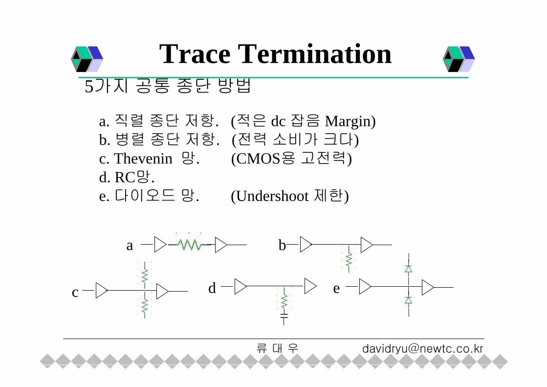
•높은 RF 에너지수준의회로와접지.•다중점접지위치.• I/O 상호연결과상호제어회로.•전력공급입력단자와시스템접지.•카드가장자리연결기와주요시스템접지.•인쇄회로기판의반대편가장자리.•케이블쉴드와 Chassis접지.
RF 접지루프의최소화

류 대 우 [email protected]
구석에서의 Trace 경로예리하게구부러진곳을만들때단위길이당용량성은증가하고반면에단위길이당유도성은감소한다.
w
C 의증가L 의값소
Bad
2:1 Ratio
Better구석의모서리를 45°각으로깎을때57%까지용량성이감소한다.
6. 추가적인설계기술

류 대 우 [email protected]
High Frequency andHigh-Speed Logic
Medium Frequencyand Medium-Speed Logic
Low Frequencyand Low-Speed Logic
Functional Layout Guidelines.

류 대 우 [email protected]
• I/0 영역 근처나 경계선을 따라 위치시키기 보다는PCB의중심부혹은접지 Stitch 위치에배치한다.
• Clock 생성 영역에 클럭 회로와 관련된 Trace만을배치한다.
• PCB 위에 직접 크리스탈과 발진기를 설치한다.
• 가능하면 전체 Clock 회로주변을신호 Trace출구를제외하고, Faraday Cage로에워싼다.

류 대 우 [email protected]
• 적절한기능적인분할이이루어져야한다.
Analog Digital
Power
Ground
Power Ground
• 분할에따른 Power와 Ground의분리가이루어져야한다.
Ex) Analog와 Digital의기능적영역사이에물리적공간을제공해야한다.

류 대 우 [email protected]
1. Shielding2. Grounding3. Balancing.4. Filtering.5. Isolation.6. Separation and orientaion.7. Circuit impedance level control.8. Cable design.9. Cancellation techniques.
7. Noise의최소화방법