Embed Size (px)
Citation preview
PrintedElectronicsandAdditiveMicroelectronicPackagingForRF/MicrowaveApplications
Prof.CraigArmientoUniversityofMassachusettsLowell
RaytheonUMassLowellResearchInstitute(RURI)PrintedElectronicsResearchCollaborative(PERC)
iMAPS NortheastWorkshop,May,2,20171
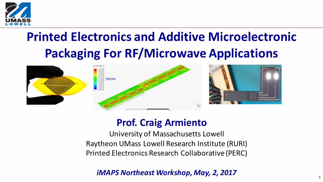
Outline
• ChallengesforPrintedElectronicsforRF/MicrowaveApplications
• PrintedElectronicsResearchthroughCorporate-AcademicPartnerships• Raytheon-UMassLowellResearchInstitute(RURI)• PrintedElectronicsResearchCollaborative(PERC)
• UniversityofMassachusettsLowell- FacilityandCapabilities
• SampleProjects• PrintedFrequencySelectiveSurfaces(FSS)• Ferroelectricinkandprintedvaractors/phaseshifters• Additivemicroelectronicpackaging• 3Dantennaarrays• Printedconnectors
• ClosingThoughts
2
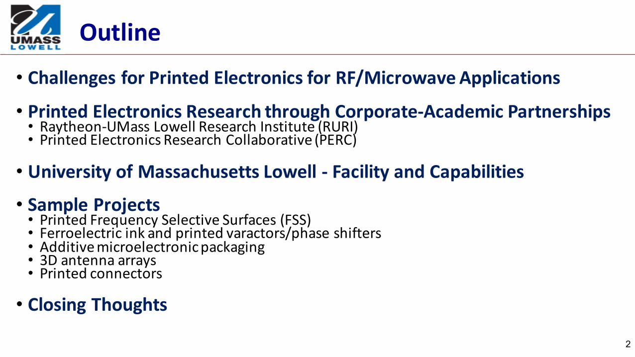
PrintedElectronicsandMicroelectronicPackaging• PrintedElectronicstechnologyworksinthedimensionalregimebetweenthesubmicron
geometriesofICsandthemuchlargerdimensionsofPCBs… whichisthescaleneededformicroelectronicpackaging
FeaturesizesICs<1micron packaging:10’sofmicrons PCBs:100’sofmicrons
• TheperformancerequirementsofRF/microwavesystemsrequirebestofbreedsemiconductoractiveICs
• PrintedRFtransistorsarenotreadyforprimetimeduetothelowmobilityofprintedsemiconductors• Microwavemodulesrequireavarietyofdifferentfunctionalitiesandrequiretheintegration
ofmanydifferentcircuitelements,interconnectsandconnectors
3
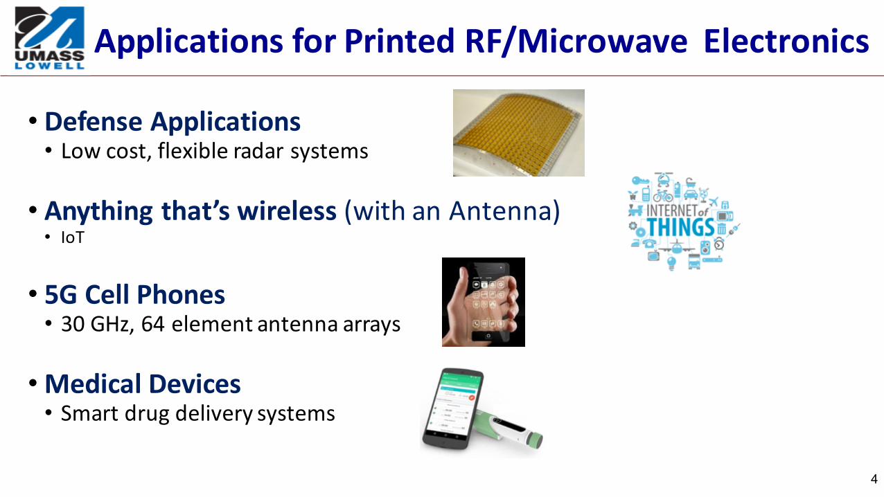
ApplicationsforPrintedRF/MicrowaveElectronics
• DefenseApplications• Lowcost,flexibleradarsystems
• Anythingthat’swireless (withanAntenna)• IoT
• 5GCellPhones• 30GHz,64elementantennaarrays
• MedicalDevices• Smartdrugdeliverysystems
4
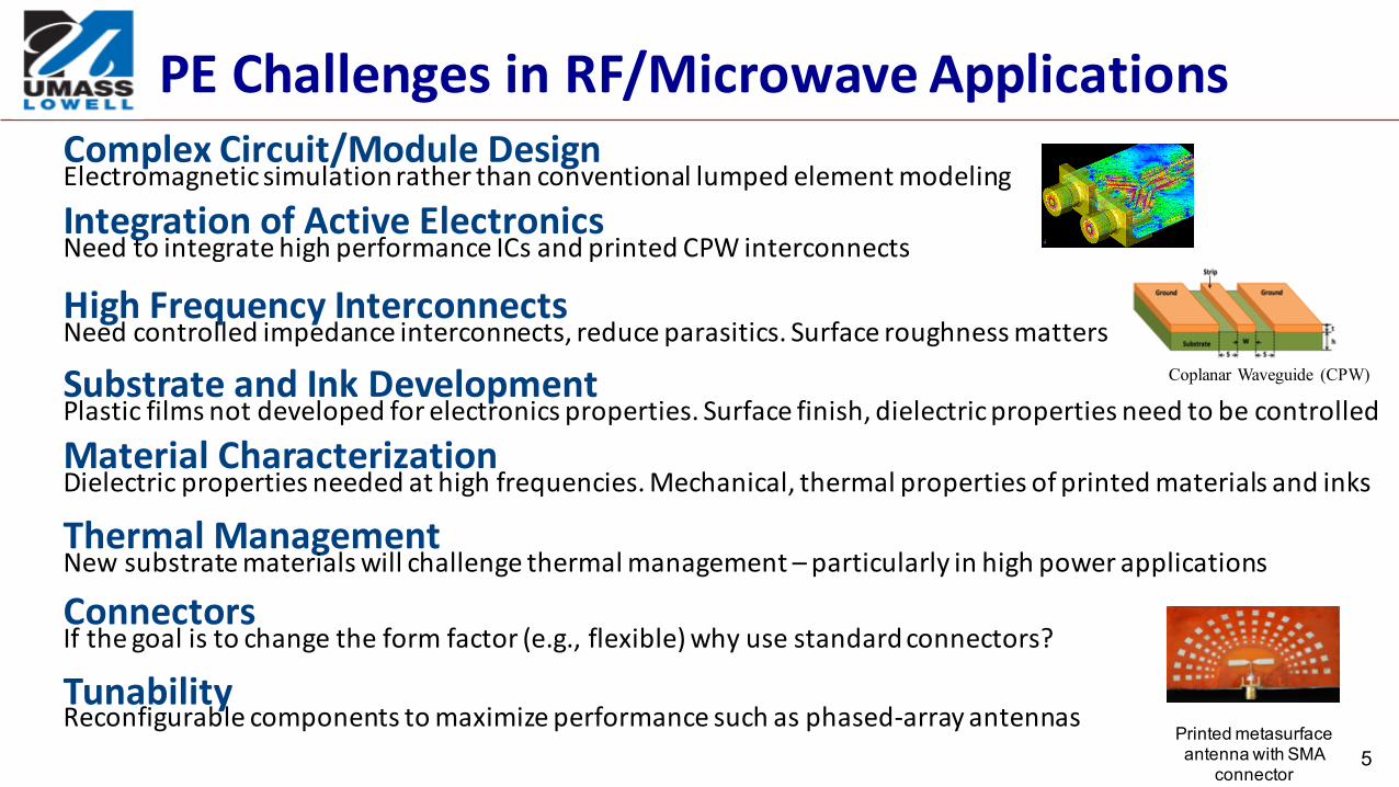
PEChallengesinRF/MicrowaveApplicationsComplexCircuit/ModuleDesignElectromagneticsimulationratherthanconventionallumpedelementmodeling
IntegrationofActiveElectronicsNeedtointegratehighperformanceICsandprintedCPWinterconnects
HighFrequencyInterconnectsNeedcontrolledimpedanceinterconnects,reduceparasitics.Surfaceroughnessmatters
SubstrateandInkDevelopmentPlasticfilmsnotdevelopedforelectronicsproperties.Surfacefinish,dielectricpropertiesneedtobecontrolled
MaterialCharacterizationDielectricpropertiesneededathighfrequencies.Mechanical,thermalpropertiesofprintedmaterialsandinks
ThermalManagementNewsubstratematerialswillchallengethermalmanagement– particularlyinhighpowerapplications
ConnectorsIfthegoalistochangetheformfactor(e.g.,flexible)whyusestandardconnectors?
TunabilityReconfigurablecomponentstomaximizeperformancesuchasphased-arrayantennas
Coplanar Waveguide (CPW)
Printed metasurfaceantenna with SMA
connector5

RURI/PERCInitiative:What&Why• ResearchFocus:PrintedElectronics(PE)&AdditiveManufacturing(AM)
• FocusonwirelessandRF/microwaveapplications• Materials,processes,devices,characterization,integratedmodeling• 2Dand3D,flexible,conformableformfactors• InitialfocusonDoDapplicationsbutexpandingtocommercialapplications
• Design,fabricateandcharacterizematerialsandprototypedevicesquickly• Acceleratesproductdesign,designerscantakemorerisk
• CorporatepartnershipsonsponsoredresearchprojectsrelatedtoAM/PE• DevelopthesupplychainforPrintedElectronics• Pursuecorporate,stateandfederalandfundingopportunities• Leverageuniversityinfrastructureandexpertise
• Plasticsengineering,nanomanufacturing• TalentAcquisition
• TrainthenextgenerationofengineersinAMandPE6

PEResearchThroughCorporate/AcademicPartnerships
• PrintedElectronicsResearchCollaborative(PERC)• PERChasraisedover$6.7Mincorporateandfederalfunds• Prepositionteamsforfederalfundingopportunities• 13companieshavejoinedPERC…morecoming
Changing the form factor and reducing cost for radar systems
Bringing the Supply Chain Together to Speed Innovation and Adoption7
• Raytheon-UMassLowellResearchInstitute(RURI)• Newco-locationmodelforuniversity-industrycollaboration• Raytheonemployeeshaveoffices,workwithUMLfaculty,students• ProjectssupportedfrominternalR&Dfunds• Significantpartnershipsinfederalfunding
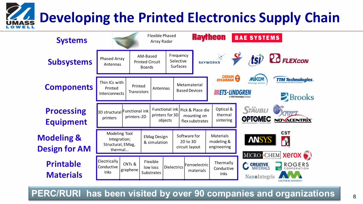
DevelopingthePrintedElectronicsSupplyChainSystems
PhasedArrayAntennas
FrequencySelectiveSurfaces
SubsystemsAM-Based
PrintedCircuitBoards
PrintedTransistors
AntennasComponents MetamaterialBasedDevices
ThinICswithPrinted
Interconnects
ThermallyConductive
Inks
PrintableMaterials
ElectricallyConductive
InksDielectrics
CNTs&graphene
FlexiblelowlossSubstrates
Ferroelectricmaterials
ProcessingEquipment
Functionalinkprinters-2D
3Dstructuralprinters
Functionalinkprintersfor3D
objects
Optical&thermalsintering
Pick&Placediemountingonflexsubstrates
Modeling&DesignforAM
EMagDesign&simulation
Softwarefor2Dto3D
circuitlayout
ModelingToolIntegration;
Structural,EMag,thermal…
Materialsmodeling&engineering
FlexiblePhasedArrayRadar
PERC/RURI has been visited by over 90 companies and organizations 8
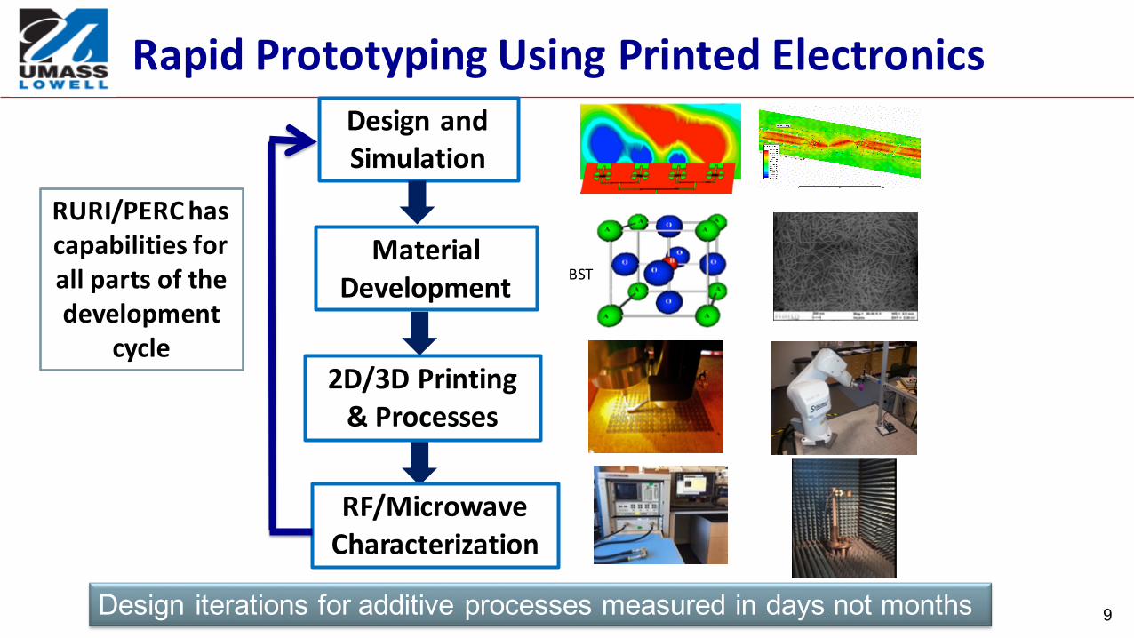
RapidPrototypingUsingPrintedElectronicsDesignandSimulation
MaterialDevelopment BST
2D/3DPrinting&Processes
RF/MicrowaveCharacterization
RURI/PERChascapabilitiesforallpartsofthedevelopment
cycle
Design iterations for additive processes measured in days not months 9
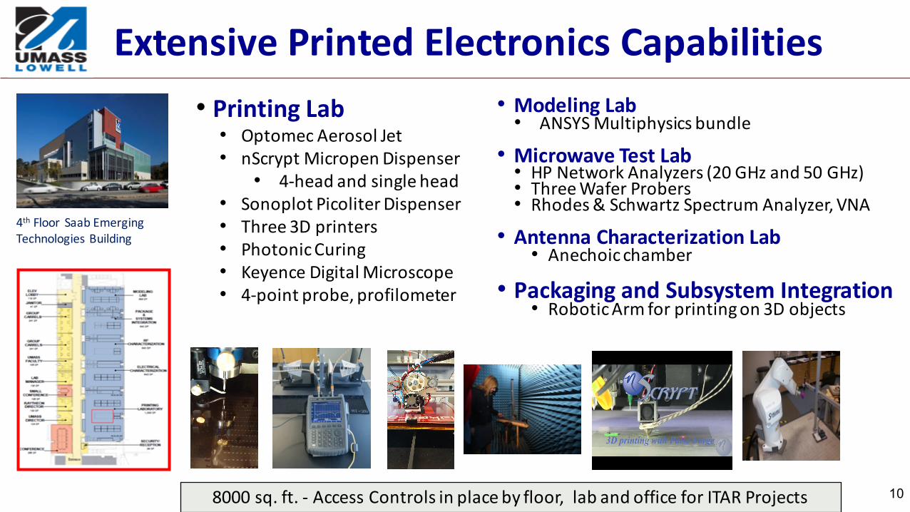
ExtensivePrintedElectronicsCapabilities• PrintingLab
• Optomec AerosolJet• nScrypt Micropen Dispenser
• 4-headandsinglehead• Sonoplot Picoliter Dispenser• Three3Dprinters• PhotonicCuring• KeyenceDigitalMicroscope• 4-pointprobe,profilometer
• ModelingLab• ANSYSMultiphysicsbundle
• MicrowaveTestLab• HPNetworkAnalyzers(20GHzand50GHz)• ThreeWaferProbers• Rhodes&SchwartzSpectrumAnalyzer,VNA
• AntennaCharacterizationLab• Anechoicchamber
• PackagingandSubsystemIntegration• RoboticArmforprintingon3Dobjects
8000sq.ft.- AccessControlsinplacebyfloor,labandofficeforITARProjects 10
4th Floor SaabEmergingTechnologies Building
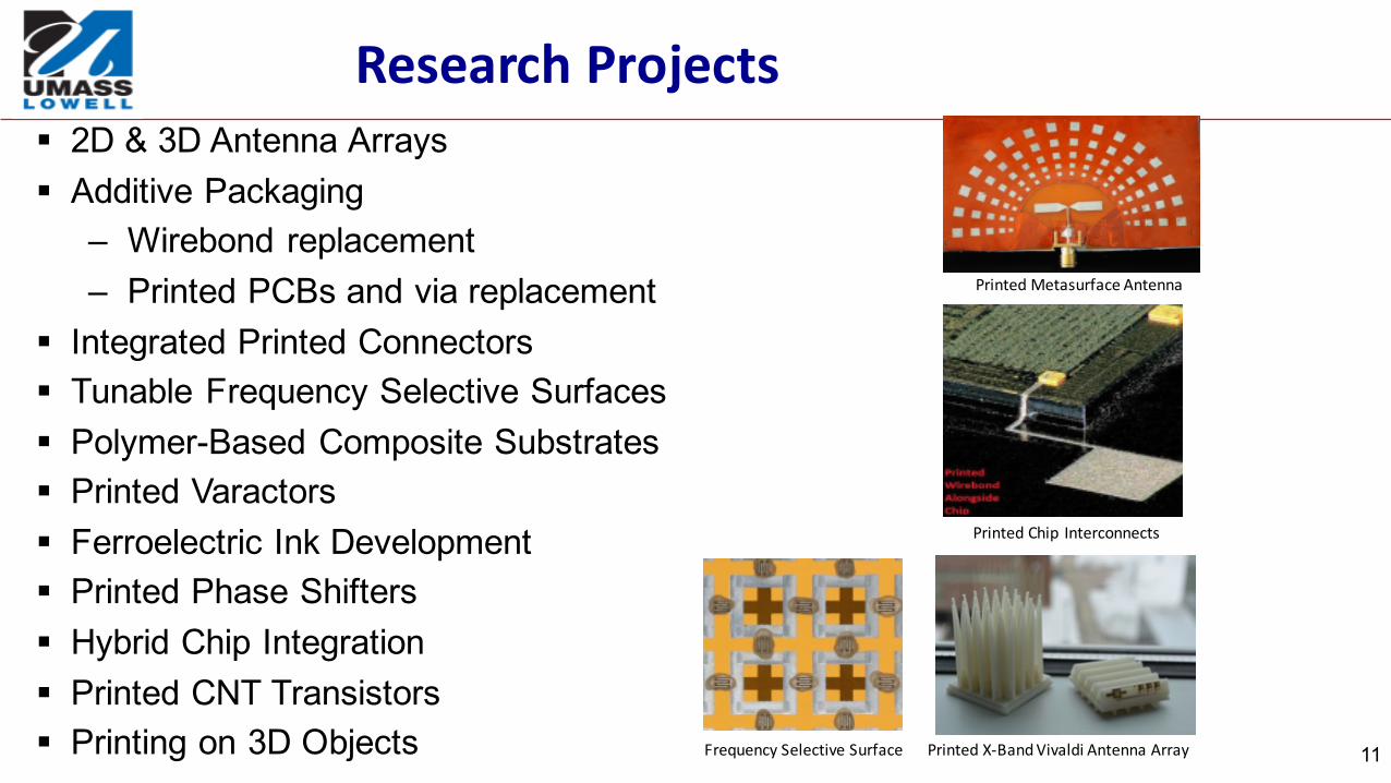
ResearchProjects§ 2D & 3D Antenna Arrays§ Additive Packaging
– Wirebond replacement– Printed PCBs and via replacement
§ Integrated Printed Connectors§ Tunable Frequency Selective Surfaces§ Polymer-Based Composite Substrates§ Printed Varactors§ Ferroelectric Ink Development§ Printed Phase Shifters§ Hybrid Chip Integration§ Printed CNT Transistors§ Printing on 3D Objects PrintedX-BandVivaldiAntennaArray
PrintedChip Interconnects
PrintedMetasurfaceAntenna
FrequencySelectiveSurface 11
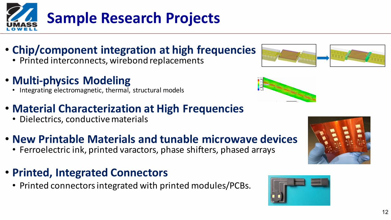
SampleResearchProjects
• Chip/componentintegrationathighfrequencies• Printedinterconnects,wirebond replacements
• Multi-physicsModeling• Integratingelectromagnetic,thermal, structuralmodels
• MaterialCharacterizationatHighFrequencies• Dielectrics,conductivematerials
• NewPrintableMaterialsandtunablemicrowavedevices• Ferroelectricink,printedvaractors,phaseshifters,phasedarrays
• Printed,IntegratedConnectors• Printedconnectorsintegratedwithprintedmodules/PCBs.
12

MaterialCharacterization:DielectricConstantvs.Frequency
Films:Free-spacecharacterization3Dprintedapparatusdesignedforholdingpolymerfilms.LensesprintedforfocusingmicrowaveexcitationforS-parametermeasurements
DielectricinkcharacterizationPrintedconcentriccapacitorsdevelopedtoextractdielectricproperties.Easysamplepreparationandsuitableforlowviscositymaterials.
Developednewcharacterizationtechniquesformeasuringthedielectricconstantandlosstangentofnovelcompositepolymersubstratesandinksoverawiderangeoffrequencies.
Solids:WaveguideMethod:DielectricblocksinsertedPLAblocksandsampleinsidetheflange(c)Waveguidemeasurementsetup
5 10 15 20 25 30Frequency (GHz)
0
1
2
3
4
Co
mp
lex P
erm
itti
vit
y '"/ '
13
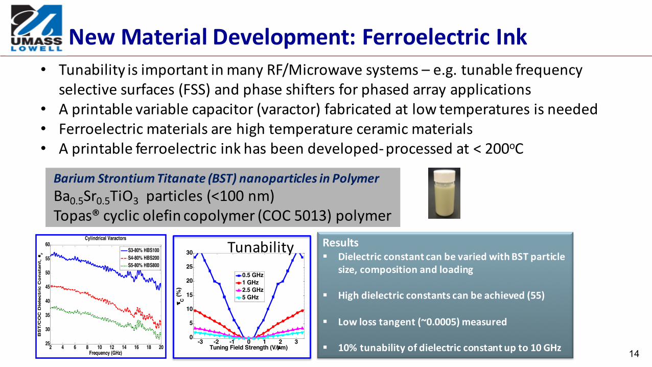
• TunabilityisimportantinmanyRF/Microwavesystems– e.g.tunablefrequencyselectivesurfaces(FSS)andphaseshiftersforphasedarrayapplications
• Aprintablevariablecapacitor(varactor)fabricatedatlowtemperaturesisneeded• Ferroelectricmaterialsarehightemperatureceramicmaterials• Aprintableferroelectricinkhasbeendeveloped-processedat<200oC
Results§ DielectricconstantcanbevariedwithBSTparticle
size,compositionandloading
§ Highdielectricconstantscanbeachieved(55)
§ Lowlosstangent(~0.0005)measured
§ 10%tunabilityofdielectricconstantupto10GHz-3 -2 -1 0 1 2 3
0
5
10
15
20
25
30Cylindrical varactor
Tuning Field Strength (V/µm)
τ C (%
)
0.5 GHz1 GHz2.5 GHz5 GHz
Tunability
2 4 6 8 10 12 14 16 18 2025
30
35
40
45
50
55
60
Frequency (GHz)
BS
T/C
OC
Die
lect
ric
Co
nst
ant,
εr
Cylindrical Varactors
S3-80% HBS100S4-80% HBS200S5-80% HBS800
BariumStrontiumTitanate(BST)nanoparticlesinPolymerBa0.5Sr0.5TiO3 particles(<100nm)Topas®cyclicolefincopolymer(COC5013)polymer
NewMaterialDevelopment:FerroelectricInk
14
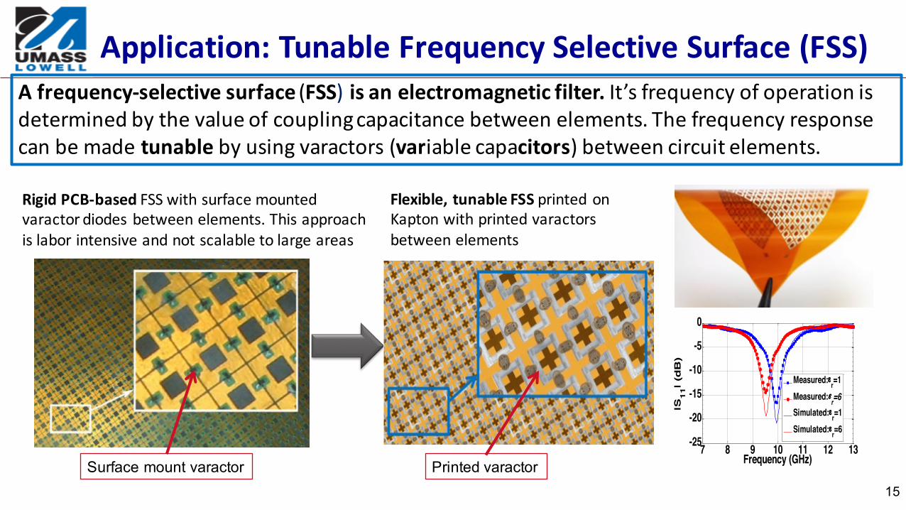
Application:TunableFrequencySelectiveSurface(FSS)
RigidPCB-basedFSSwithsurfacemountedvaractor diodesbetweenelements.Thisapproachislaborintensiveandnotscalabletolargeareas
Afrequency-selectivesurface (FSS)isanelectromagneticfilter. It’sfrequencyofoperationisdeterminedbythevalueofcouplingcapacitancebetweenelements.Thefrequencyresponsecanbemadetunable byusingvaractors (variablecapacitors)betweencircuitelements.
Surface mount varactor
Flexible,tunableFSSprintedonKapton withprintedvaractorsbetweenelements
Printed varactor15
7 8 9 10 11 12 13-25
-20
-15
-10
-5
0
Frequency (GHz)
|S1
1| (d
B)
Measured:εr=1Measured:εr=6Simulated:εr=1Simulated:εr=6
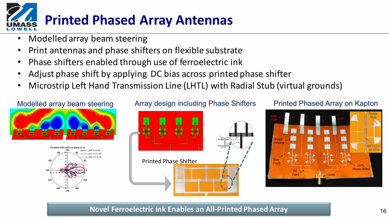
PrintedPhasedArrayAntennas• Modelledarraybeamsteering• Printantennasandphaseshiftersonflexiblesubstrate• Phaseshiftersenabledthroughuseofferroelectricink• AdjustphaseshiftbyapplyingDCbiasacrossprintedphaseshifter• Microstrip LeftHandTransmissionLine(LHTL)withRadialStub(virtualgrounds)
PrintedPhaseShifter
Modelled array beam steering Array design including Phase Shifters Printed Phased Array on Kapton
NovelFerroelectricInkEnablesanAll-PrintedPhasedArray 16
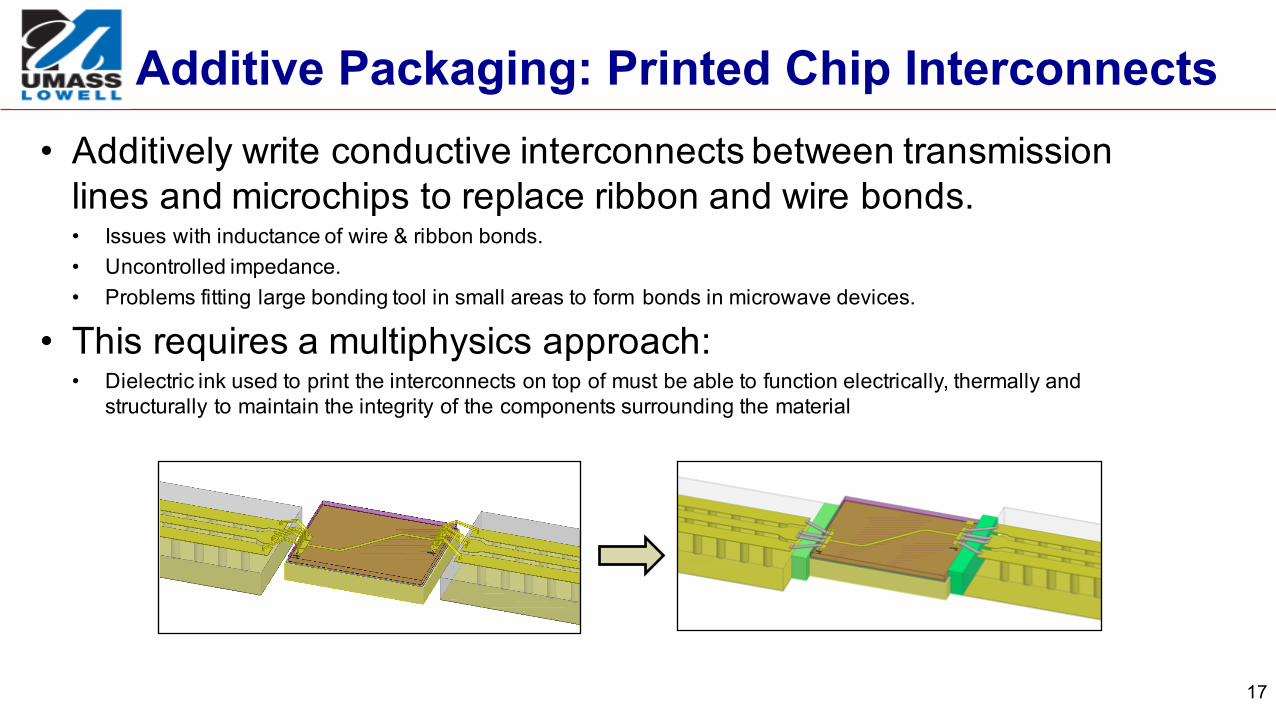
Additive Packaging: Printed Chip Interconnects• Additively write conductive interconnects between transmission
lines and microchips to replace ribbon and wire bonds.• Issues with inductance of wire & ribbon bonds.• Uncontrolled impedance.• Problems fitting large bonding tool in small areas to form bonds in microwave devices.
• This requires a multiphysics approach:• Dielectric ink used to print the interconnects on top of must be able to function electrically, thermally and
structurally to maintain the integrity of the components surrounding the material
17
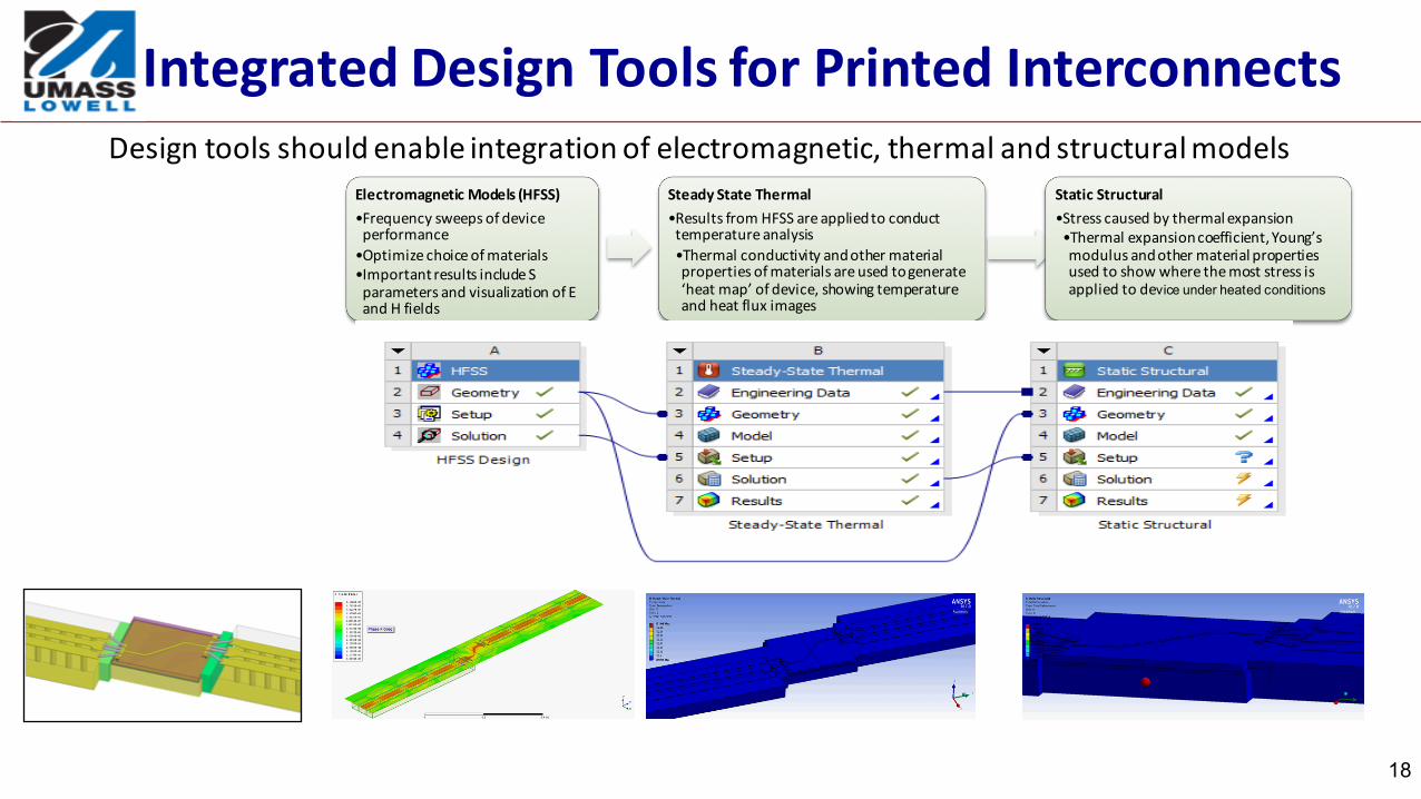
IntegratedDesignToolsforPrintedInterconnects
ElectromagneticModels(HFSS)•Frequencysweepsof deviceperformance•Optimizechoiceofmaterials•ImportantresultsincludeSparametersandvisualizationofEandHfields
SteadyStateThermal•ResultsfromHFSSareappliedtoconducttemperatureanalysis•Thermalconductivityandothermaterialpropertiesofmaterialsareusedtogenerate‘heatmap’ofdevice,showingtemperatureandheatfluximages
StaticStructural•Stresscausedbythermalexpansion•Thermalexpansioncoefficient,Young’smodulusandothermaterialpropertiesusedtoshowwherethemoststressisappliedtodevice under heated conditions
Designtoolsshouldenableintegrationofelectromagnetic,thermalandstructuralmodels
18
19
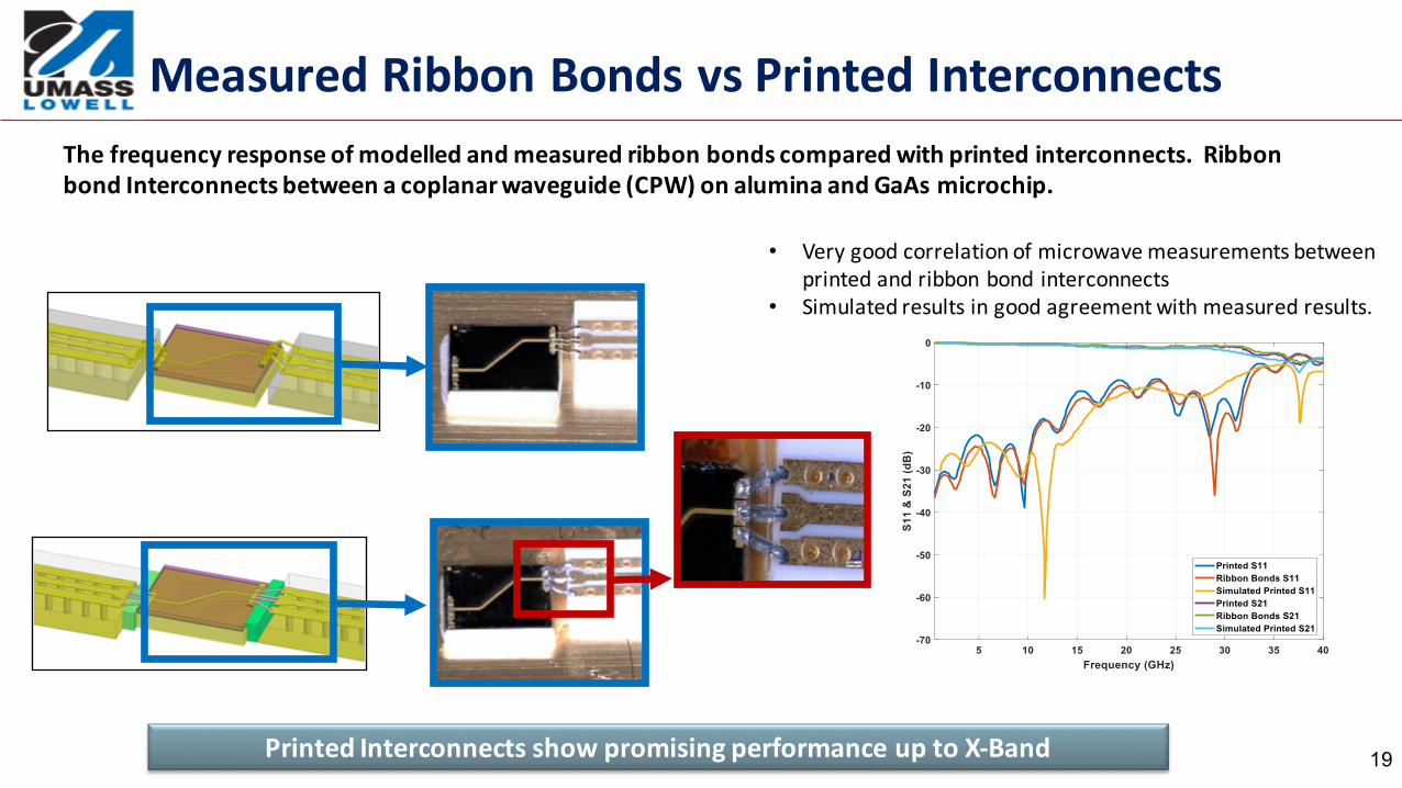
MeasuredRibbonBondsvsPrintedInterconnectsThefrequencyresponseofmodelledandmeasuredribbonbondscomparedwithprintedinterconnects.RibbonbondInterconnectsbetweenacoplanarwaveguide(CPW)onaluminaandGaAsmicrochip.
• Verygoodcorrelationofmicrowavemeasurementsbetweenprintedandribbonbondinterconnects
• Simulatedresultsingoodagreementwithmeasuredresults.
PrintedInterconnectsshowpromisingperformanceuptoX-Band
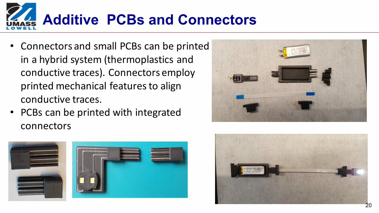
Additive PCBs and Connectors• ConnectorsandsmallPCBscanbeprintedinahybridsystem(thermoplasticsandconductivetraces).Connectorsemployprintedmechanicalfeaturestoalignconductivetraces.
• PCBscanbeprintedwithintegratedconnectors
20
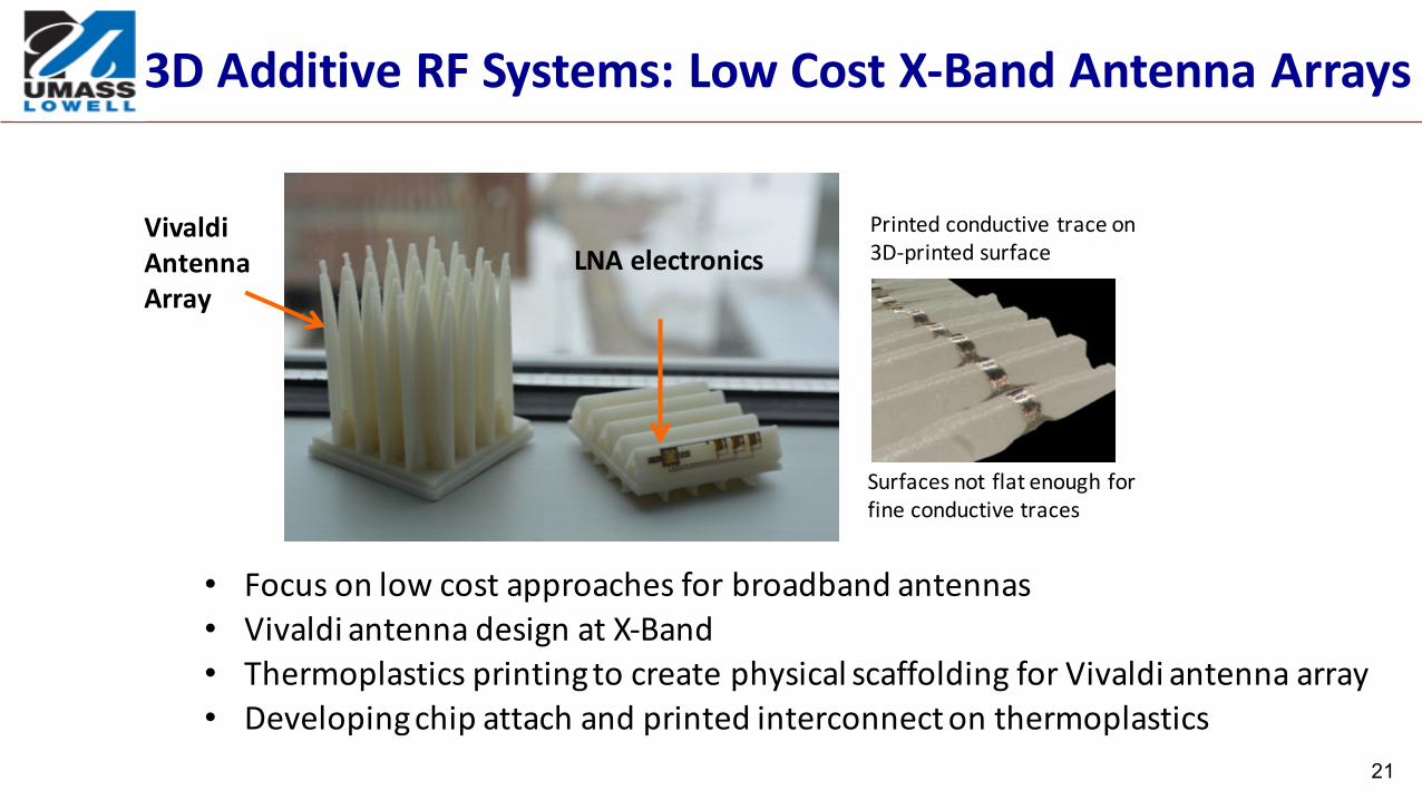
3DAdditiveRFSystems:LowCostX-BandAntennaArrays
VivaldiAntennaArray
LNAelectronics
• Focusonlowcostapproachesforbroadbandantennas• VivaldiantennadesignatX-Band• ThermoplasticsprintingtocreatephysicalscaffoldingforVivaldiantennaarray• Developingchipattachandprintedinterconnectonthermoplastics
Printedconductivetraceon3D-printedsurface
Surfacesnotflatenoughforfineconductivetraces
21
FinalThoughts• PrintedElectronicsformicrowaveapplicationsisinthe“WildWest”phase
• Incoherentsupplychain• Lackofstandards,materials,models,SW• Developmentofprintedsubsystemsinthemicrowavedomainintroduces
additionalchallengesineveryphase(design,materials,printing&characterization)
• WillneedtodevelopthesupplychainforPEtechnologysimilartoICmanufacturersinthe60’s&70’s
• Partnershipsbetweencompanies,government(stateandfederal)anduniversitiescanacceleratethebuildoutoftheecosystemforprintedelectronics
RURIandPERCbringindustry,academiaandsupplychaintogethertoaccelerateinnovationandadoptionofprintedelectronicsformicrowaveapplications.
22
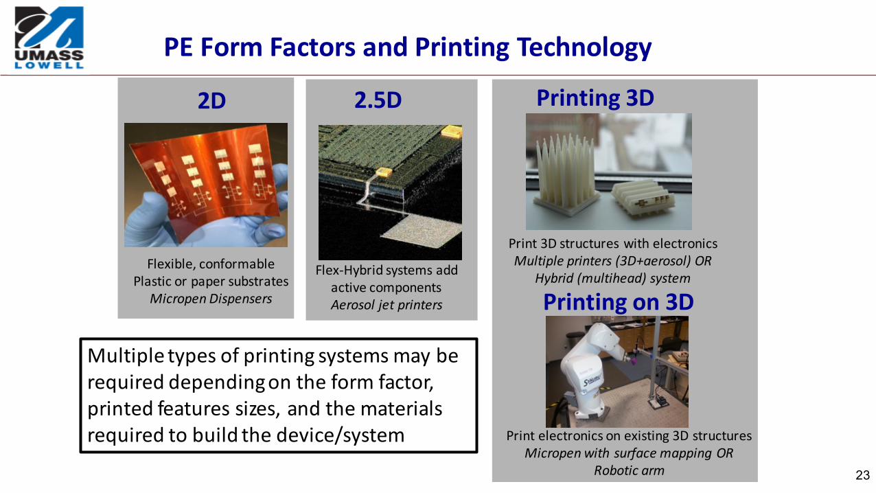
PEFormFactorsandPrintingTechnology
Flex-HybridsystemsaddactivecomponentsAerosoljetprinters
2.5D
Flexible,conformablePlasticorpapersubstrates
Micropen Dispensers
2D
Multipletypesofprintingsystemsmayberequireddependingontheformfactor,printedfeaturessizes,andthematerialsrequiredtobuildthedevice/system Printelectronicsonexisting3Dstructures
MicropenwithsurfacemappingORRoboticarm
Printing3D
Print3DstructureswithelectronicsMultipleprinters(3D+aerosol)OR
Hybrid(multihead)system
Printingon3D
23