Embed Size (px)
Citation preview

HAL Id: cel-00667574https://cel.archives-ouvertes.fr/cel-00667574v2
Submitted on 8 Feb 2012
HAL is a multi-disciplinary open accessarchive for the deposit and dissemination of sci-entific research documents, whether they are pub-lished or not. The documents may come fromteaching and research institutions in France orabroad, or from public or private research centers.
L’archive ouverte pluridisciplinaire HAL, estdestinée au dépôt et à la diffusion de documentsscientifiques de niveau recherche, publiés ou non,émanant des établissements d’enseignement et derecherche français ou étrangers, des laboratoirespublics ou privés.
Process simulation for advanced stress and junctionengineering
Christophe Krzeminski, Evelyne Lampin
To cite this version:Christophe Krzeminski, Evelyne Lampin. Process simulation for advanced stress and junction engi-neering. École thématique. ESSDERC/ESSCIRC 2008 Tutorial Session T2 Nanoelectronics : Charac-terisation for the nanoelectronics era, Edinburgh, UK, 2008, 53 p. <cel-00667574v2>

1
PRÉSENTATION
ESSDERC/ESSCIRC Tutorial 2008: Characterisation for the nanoelectric era
Process simulation for advanced stress and junction engineering
Christophe Krzeminski and Evelyne Lampin
Email: [email protected]
IEMNUMR CNRS 8520
59652 Villeneuve d’Ascq
France

2
Tutorial objectives
“Process simulation for advanced stress and junction engineering »
»Large topic and only 45 minutes !»and 53 slides
» Why Simulation in a characterisation tutorial ?»Complementary...
»Not a so good idea to go deeply in the modeling aspect»Overview of the field: the challenge (Part I), status (Part II), progress (Part III & IV) and perspectives (Part V)
»No equation

3
Outline
Part I: Introduction: Challenge and solution for downscaling
Part II: Process simulation ?
Part III: Recent progress in the modeling of stress
Part IV: Recent progress in the modeling of junction engineering
Part V: Perspectives in Atomistic TCAD: towards some atomistic experiment ?

4
PART I
Part I Introduction: Challenge and solution for downscaling

5
Downscaling (→ 90 nm)
S. E. Thompson et al., IEEE Trans. On Semiconductor Manufacturing, Vol. 18, n°1, 2005

6
Downscaling (→ 90 nm)
W. Haensch et al., IBM J. Res&Dev, Vol. 50, n°45, 2006

7
Stress Engineering approach
• (90nm→ ?)
Main idea: Strain engineering for enhanced mobility and drive current
Mohta et al., IEEE Circuits and Magazine 2005 L. Peters,“ Options Narrow at 45nm”, Semiconductor International,2006
8
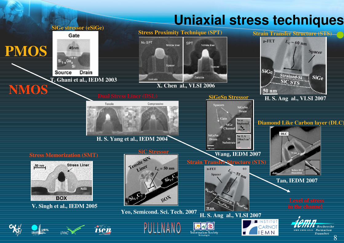
Uniaxial stress techniques
V. Singh et al., IEDM 2005
T. Ghani et al., IEDM 2003
Yeo, Semicond. Sci. Tech. 2007
Wang, IEDM 2007
Tan, IEDM 2007
H. S. Yang et al., IEDM 2004
X. Chen al., VLSI 2006
SiGe stressor (eSiGe)
Dual Stress Liner (DSL)
Diamond Like Carbon layer (DLC)
Stress Memorization (SMT)
Stress Proximity Technique (SPT)
SiC Stressor
SiGeSn Stressor
Strain Transfer Structure (STS)
Strain Transfer Structure (STS)
H. S. Ang al., VLSI 2007
H. S. Ang al., VLSI 2007
Level of stressin the channel
PMOS
NMOS

9
Junction optimisation
RcontactRsheet R sp
reading
Raccumulation
RcontactRsheet R sp
reading
Raccumulation
J. O. Borland, « 32 nm NODE USJ Implant& Annealing, RTP 2007 RSheet: Conductivity of high doped region High activation: complex techniques
10
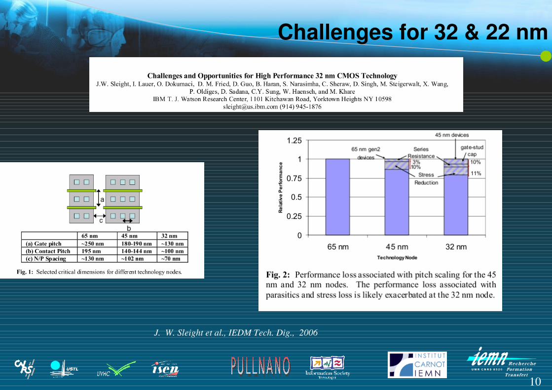
Challenges for 32 & 22 nm
J. W. Sleight et al., IEDM Tech. Dig., 2006

11
Challenges for 32 nm
• Scalability:– 11% stress reduction compared to 65nm (decreasing gate pitch) [Sleight06]
– ITRS Junction target (extension depth, abruptness& sheet resistance) challenging
• Yield: – ITRS[07] : integration of multiple sources of local and global stress – Not exceeding the local critical shear stress
• Design– Pitch and layout dependent– “Strain adds new challenges from a design perspective” [Lammers08]
→ TCAD have a role to play to provide key information (process => design)

12
PART II
PART II: Process Simulation ?

13
TCAD ?
TCAD :↘ Technology cost development (40% ITRS) ↗ Yield
14
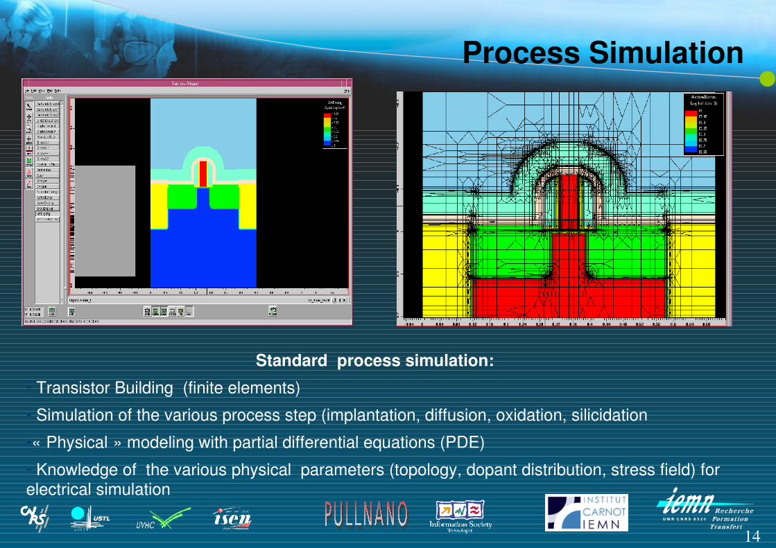
Process Simulation
Standard process simulation: Transistor Building (finite elements)
Simulation of the various process step (implantation, diffusion, oxidation, silicidation
« Physical » modeling with partial differential equations (PDE)
Knowledge of the various physical parameters (topology, dopant distribution, stress field) for electrical simulation

15
Implantation modelingImplantation modeling : Implant tables or MonteCarlo Simulation
M. Posselt, private communication
Series of consecutive binary collisions of the projectile with the lattice (BCA MC):
Nuclear scattering (Coulomb pair potential )Semi empirical model for the electronic energy loss of particlesPhenomenological models for damage probability
Range distribution of implanted ions
Damage profile

16
Implantation Modeling Example
• 2D Implant modeling for nanowire fabrication
Vikram Passi et al., UCL, NANOSIL WP 2.1 (unpublished results)
Creation of Silicon nanowire by anisotropic etching with a damage gradient Optimisation (Dopant, Dose, Energy) with simulation

17
Standard Technology
Junction Fabrication
Diffusion modeling (1)
Ionic implantation for the dopant with various energy& dose
After implantation:
● Dopants in an interstistial position electrically inactive
● Defects created : interstitials, vacancies, aggregate, amorphous pocket
→ Annealing step mandatory
Boron atoms

18
Boron Kickout
Diffusion Modeling (2)
What's going on during annealing? Example for boron
• The junction depth and the activated dose results from the contribution of all these mechanisms
• Interstitial Boron mobile form
• Immobile Boron impurity (electrically active) and creation of Si interstitial
• Diffusion and recombinaison of Si interstitial.
• Kickout of a boron atoms by an another Si interstitial
• …
• Standard process simulator used Fick law and diffusion reaction equations to describe the the intreaction with point defects and mechanism like kickout

19
Diffusion Modeling (3)• Application: Evolution of doping profile during annealing
critical for electrical properties (see also slide 44)
Example of Boron diffusion profile diffusion

20
Oxidation and stress modeling (1)
Process simulator : generalised Deal& Grove oxidation model ( diffusivity & and reaction rate stressdependent) to take into account the stress (volume expansion)

21
Various source of stress
Example : modeling of stress generated by deposition of thin film
introduction of an extrinsic stress and mechanical equilibration
Steep doping gradientsHigh doping induced stress
Structural modifications of films Extrinsic stress
Film deposition process (nitride, polysilicon, metals….)
Intrinsic Stress
Thermal growth (oxidation, silicidation), etching
Topological induced Stress
Thermal variation during various processing step
Thermal Stress
Technical ProcessStress sources
Si subtrate
Film
σextrinsic

22
Example: Oxidation and stress modeling
STI (Shallow stress Isolation structure)
Stress field (TCAD) μRS (experiment vs simulation)
but for Large structure
23
Conclusion
• These different examples => process modeling promising• Reality is/was more complex (2002)
– Example taken from different or academic softwares– Difficulty to describe TED Boron, segregation effects, ultrathin oxidation,
silicidation....– No real stress modeling capabilities (commercial tool)
• The Mark Law definition: « TCAD : yesterday’s technology modeled tomorrow»
M. E. Law, IBM J. Res. Dev., Vol. 46, n°2/3, March 2002

24
Conclusion• « TCAD : yesterday’s technology modeled tomorrow» still true ?• No:
– Large progress have been performed in diffusion modeling ( Support by the EC: European project Rapid, Frendtech, PullNaNo,Atomics)
– Progress have been done for « simple » stress modeling
– The merging of the major TCAD firms (Avant!, ISE, Synopsys) ~ market 80% DIOS (meshing, numerical stability), TAURUS (3D capabilities, Implantation,
stress) and TSUPREMIV (oxidation modeling) to the FLOOPSISE (new diffusion modeling)
– More contribution and more insight with atomistic modeling – There is also a part of « dream »: simulation can not replace characterisation
– Script models speed up the pipeline (M. Law) : University (models)=>TCAD company (software) => Semiconductor Company ? No but more
• Yes:– Complexity increase : Stress Engineering (Slide 8), New material (Ge), Laser
Annealing & Solid Phase Epitaxy.....

25
PART III
Recent progress in the modeling of stress
26
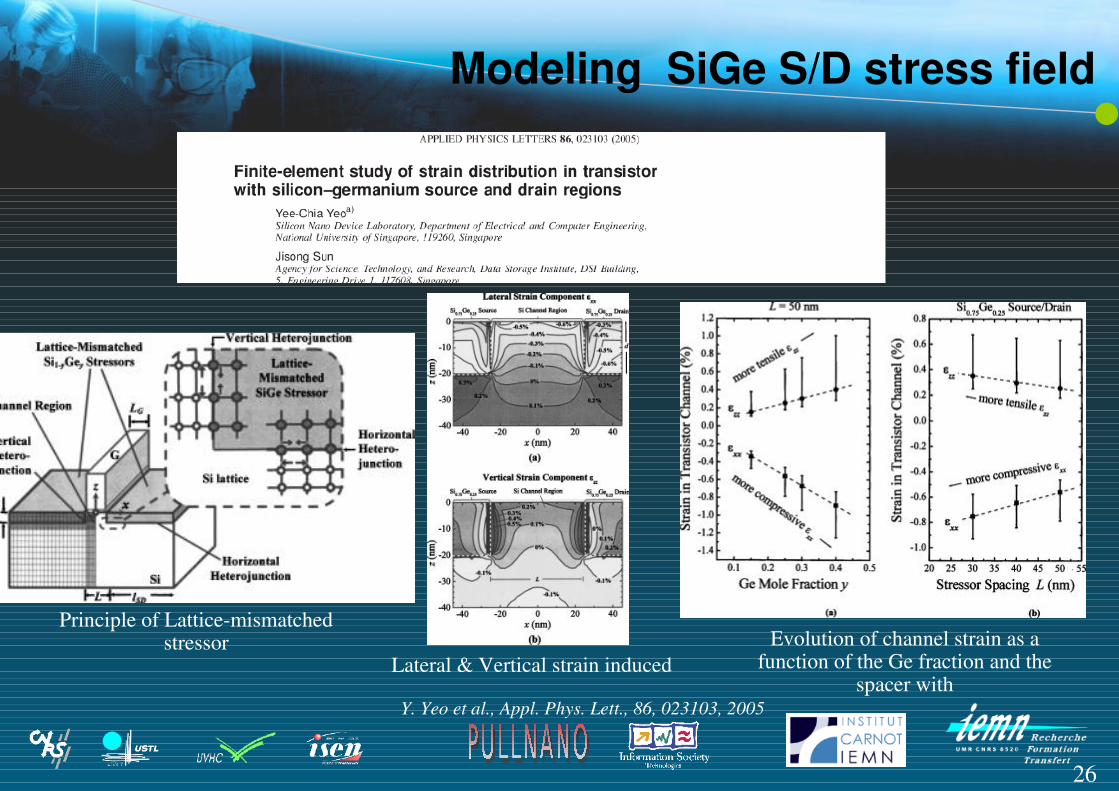
Modeling SiGe S/D stress field
Y. Yeo et al., Appl. Phys. Lett., 86, 023103, 2005
Principle of Latticemismatched stressor
Lateral & Vertical strain inducedEvolution of channel strain as a
function of the Ge fraction and the spacer with

27
SiGe S/D scalability
G. Eneman et al., IEEE Trans. on Electron Device, Vol. 86, 023103, 2005
Mean compressive channel stress does not decrease with downscaling

28
Modeling CESL stress
K. V. Loiko et al., SISPAD 2006
Large difference between mono and multi step deposition
Opposite experimental trends with mono step deposition !
→
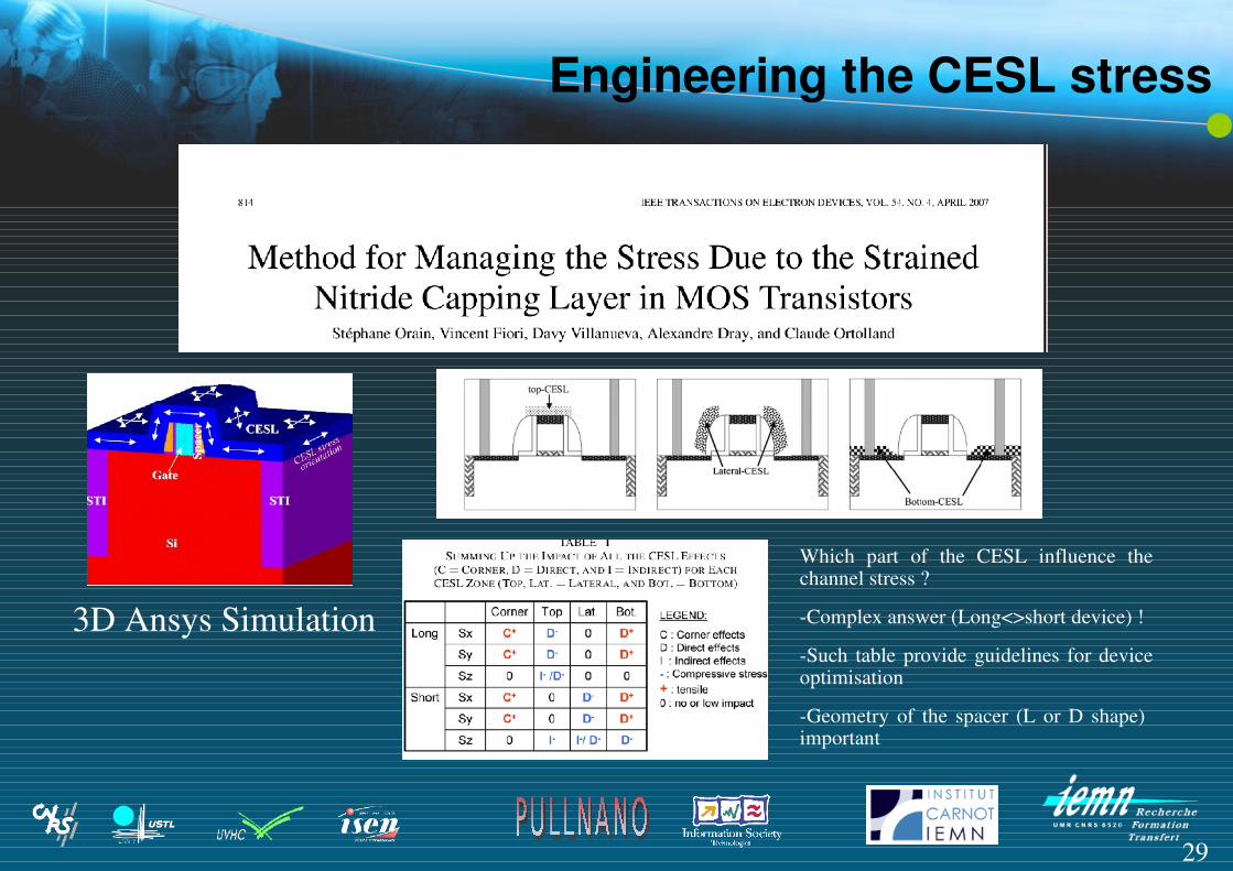
29
Engineering the CESL stress
3D Ansys Simulation
Which part of the CESL influence the channel stress ?
Complex answer (Long<>short device) !
Such table provide guidelines for device optimisation
Geometry of the spacer (L or D shape) important

30
Scalability of CESL
↘ CESL thickness is no sufficient, spacer dimensions must be scaled
Poly to Poly Distance: Lp/p
For large CESL thickness, decreasing Lp/p leads to stress reduction
Influence of spacer width on vertical stress for decreasing Lp/p
G. Eneman et al., IEEE Trans. on Electron Device, Vol. 54, N°6, June, 2007

31
Si 0.85 Ge 0.15
No CESL
Si 0.85 Ge 0.15
CESL
Si 0.75 Ge 0.25
CESL
Si 0.75 Ge 0.25
no CESL
640 Mpa
460 Mpa
930 Mpa
730 Mpa
C. Krzeminski , PULLNANO Results (unpublished)
S/D SiGe & CESL modeling with SProcess

32
Conclusion
• Large progress have been performed in the stress modeling with the support of experimental development, study of topography influence, evaluation of scalability (SiGe S/D or Stress Liner)
• There was one issue :
• But large progress have been performed recently in the last version of Sentaurus Process as shown by the last PullNANO Results
• Still a lot of work: Stress Memorization, SiC stressor.....
Journal or majorproceedings conferencesPublications (20012008)
Number Proprietarysimulator
“Old” simulator Taurus/ TsupremIV
Mechanical simulator(Ansys/ FEMLAB)
SentaurusProcess
TCAD&stress 14 30% 40% 30% 0%
33
Part IV
Progress in diffusion modeling

34
Role on extended defects formed after ion implantation of dopants
Bongiorno, Europhys. Lett.
50, 608 (2000).
2 atoms
~ 10000atoms
CEMES/LAAS
Kim, Phys. Rev. Lett. 84, 503 (2000).
{113} defects
Small clusters
Dislocation loops
Claverie, Mat. Sc. Semicond. Proc. 3, 269 (2000).
Cherkashin, MRS Symp. Proc. 810, C3.7 (2004).
Claverie, MRS Symp. Proc. 610, B11.6 (2000).
Extended defects

35
Boron Transient enhanced diffusion (TED) & extended defects→ Common origin : the supersaturation of interstitials formed by the implantation step
Ex in the case of a preamorphisation :
Amorphous Si
crystalExcess or supersaturation of interstitials just behind the amorphous /cristalline interface
During annealing :
Precipitation into extended defects
Accelerated diffusion of boron
→ Need to couple a model of extended defects to conventionnal packages of dopant diffusion

36
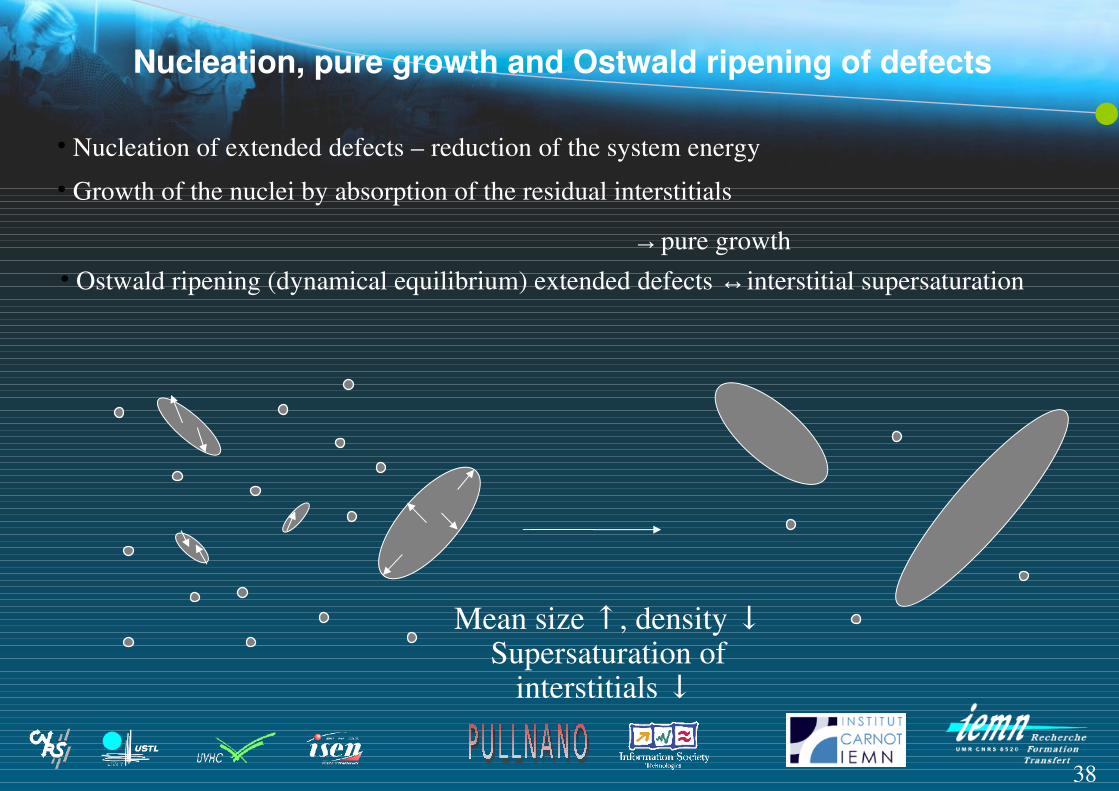
nucleation, pure growth and Ostwald ripening of defects
• Nucleation of extended defects – reduction of the system energy
Precipitation

37
• Growth of the nuclei by absorption of the residual interstitials
→ pure growth
Growth of the existing defectsSupersaturation ↓
nucleation, pure growth and Ostwald ripening of defects
• Nucleation of extended defects – reduction of the system energy
38
• Ostwald ripening (dynamical equilibrium) extended defects ↔interstitial supersaturation
Mean size ↑, density ↓Supersaturation of
interstitials ↓
• Growth of the nuclei by absorption of the residual interstitials
→ pure growth
Nucleation, pure growth and Ostwald ripening of defects
• Nucleation of extended defects – reduction of the system energy

39
TED and Dislocation Loops (DL)
Evolution of density and size of Dislocations loops (DL)
Final TED diffusion effects underestimated if DL not
considered
Good predictivity of TED effects with the incorparation of DL and Si interstitials evolution

40
Atombyatom model of defects evolution
Ex : n=4
A. Claverie et al., Appl. Phys. A, Vol. 76, 2003 (Frendtech results)
Formation energies for clusters, {113} Cowern et al.
Dissolution of {113}'s Evolution of Si interstitials as a function of the time
41
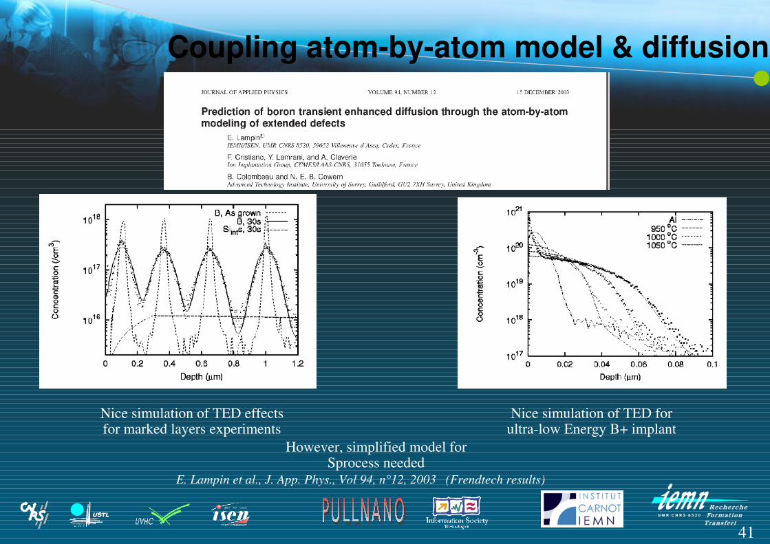
Coupling atombyatom model & diffusion
E. Lampin et al., J. App. Phys., Vol 94, n°12, 2003 (Frendtech results)
Nice simulation of TED effects for marked layers experiments
Nice simulation of TED for ultralow Energy B+ implant
However, simplified model for Sprocess needed

42
Advanced annealing schemes
J. Shermer et al., ESSDERC 2007 (PULLNANO results)

43
Boron diffusion modeling & Device simulation
P. Pichler et al., International Workshop on junction Technology (2008), ATOMICS & PULLNANO Results
FD nanometric SOI device Impact of the diffusion modeling on the boron profile
Large impact on the PMOS electrical characteristic
predicted

44
Conclusion
• Large progress have been done in junction processing modeling in the framework of several european projects (Rapid, Frendtech, Pullnano, Atomics) with the collaboration of Synopsys (Zurich)
• Some of the models presented (simplified form) in Sentaurus Process or script transfered to semiconductor compagnies
• But still a lot of work:– Influence of stress effects – New Material (SiGe S/D, Ge....)– Advanced annealing scheme (laser annealing, solid phase epitaxy)
• More information :

45
Part V (prospective)
Atomistic TCAD : towards some computer experiment ?

46
Complexity &Limits of a full experimental optimisation (1) ?
•Complex integration in nanodevices
(PULLNANO results)
47
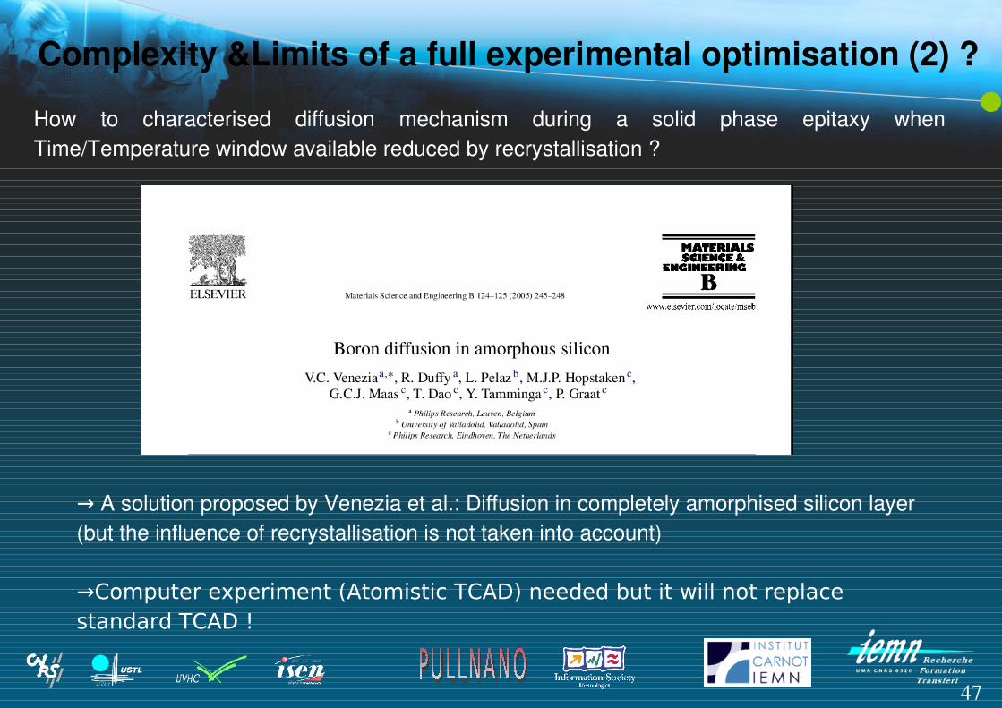
How to characterised diffusion mechanism during a solid phase epitaxy when Time/Temperature window available reduced by recrystallisation ?
→ A solution proposed by Venezia et al.: Diffusion in completely amorphised silicon layer (but the influence of recrystallisation is not taken into account)
→Computer experiment (Atomistic TCAD) needed but it will not replace standard TCAD !
Complexity &Limits of a full experimental optimisation (2) ?

48
Which method for computer experiment ?
[Scheerschmidt07] http://www.mpihalle.de/mpi/publi/pdf/6735_06.pdf
Development of atomistic approach based on molecular dynamics (MD)
49
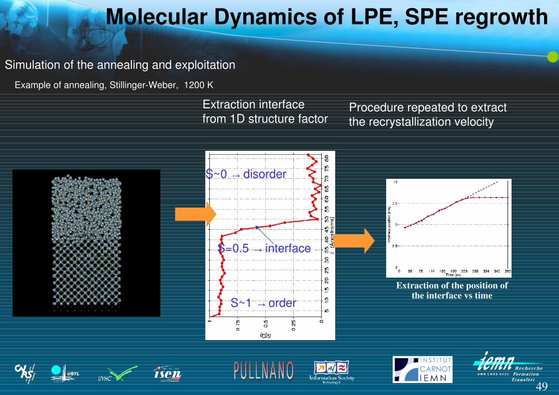
Example of annealing, StillingerWeber, 1200 K
Molecular Dynamics of LPE, SPE regrowth
Simulation of the annealing and exploitation
Extraction interface from 1D structure factor
Procedure repeated to extract the recrystallization velocity
S~1 → order
S~0 → disorder
S=0.5 → interface
Extraction of the position of the interface vs time

50
LPE
SPE
Conclusion :
Potentiality to simulate both SPE and LPE
Analysis of the velocities of recrystallization and of the structure of disordered part :
C. Krzeminski, Q. Brulin, V. Cuny, E. Lecat, E. Lampin et al, J. Appl. Phys. 101, 123506 (2007)
SPER or flash annealing
Laser annealing
Molecular dynamics of SPE, LPE regrowth (2)
(PULLNANO results)
51
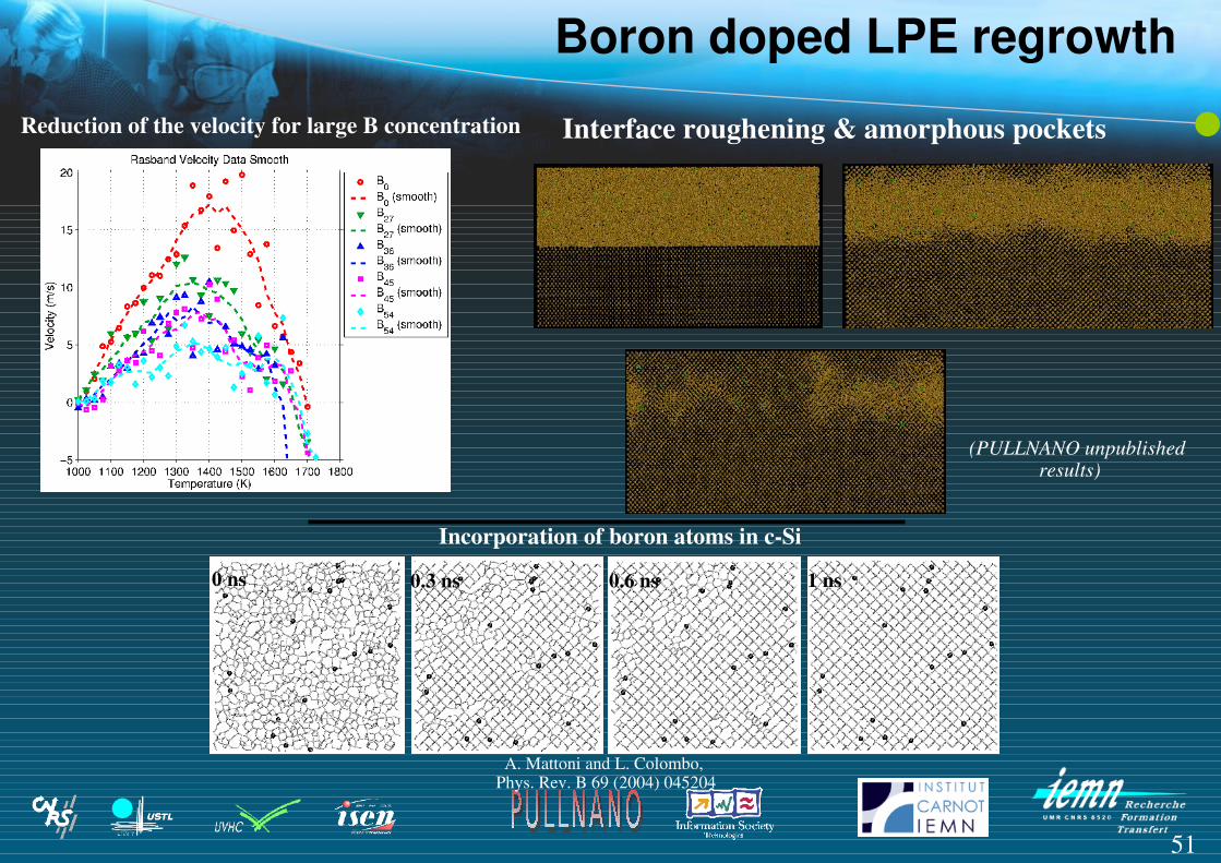
Reduction of the velocity for large B concentration
Incorporation of boron atoms in cSi
A. Mattoni and L. Colombo, Phys. Rev. B 69 (2004) 045204
0 ns 0.3 ns 0.6 ns 1 ns
Boron doped LPE regrowth
Interface roughening & amorphous pockets
(PULLNANO unpublishedresults)

52
LPE or SPE: influence orientation effects
Orientation influence for SPE [100]>[110]>[111]Orientation influence for LPE [100]>[110]>[111]
(PULLNANO unpublished results)

53
30 ns 60 ns 80 ns
Some grains begin to form by RNG
Thick amorphous layer
Thin crystalline germCrystallization has progressed by SPE
Competition SPE/RNG
(PULLNANO unpublished results)