Embed Size (px)
Citation preview

1
EE M216A .:. Fall 2010Lecture 5
Logical Effort
Prof. Dejan Marković[email protected]
Logical Effort Recap
Normalized delay– d = g·h + p– g is the logical effort of the gate
g C /C● g = CIN/CINV
● Inverter is sized such that RINV equals the gate’s drive strength
– h is the electrical effort● h = COUT/CIN
● The combination of g·h is essentially our fan‐out definition
– p is the parasitic effort● p = CSELF/CINV
D. Markovic / Slide 2
p SELF/ INV
● Typically ~1 for an inverter
May have different g, p for each type of gate structure– The g, p may differ per input, and for pull‐up/down
EEM216A .:. Fall 2010 Lecture 5: Logical Effort | 2

2
A Side Note: Total Gate Effort (gTOT)
One way of evaluating a gate is to look at the total logical effort of the gate– gTOT = CIN_TOT/CINV
● A sum of the total input capacitance● A sum of the total input capacitance
– Example:● 3‐input NAND● Equivalent inverter is 4:2● gINPUT = 10/6=5/3● gTOT = 30/6 = 5 (or 3·gINPUT)
WP:WN = 4:6
D. Markovic / Slide 3
The total gate effort is not very useful to calculate delay– But it is an indication of the “cost” of the gate– Can be very useful in gate mapping of logic synthesis
● To find which gate is best to use to map a given Boolean expression
EEM216A .:. Fall 2010 Lecture 5: Logical Effort | 3
A Note on Asymmetry
The gates used in examples so far have been symmetric– All inputs are essentially identical
● Some are bundled
P:N ratio is approximately equal to the mobility ratio– P:N ratio is approximately equal to the mobility ratio● Same as the reference inverter
The truth is that inputs of most gates are not symmetric– Different inputs may see different capacitances– Even series stacked gates may not be the same size
Pull‐up and pull‐down is rarely equal resistanceC ll thi “ k d” t
D. Markovic / Slide 4
– Call this “skewed” gates– P:N sizing for optimal delay is β = root(µ)– Inverter in a domino gate often favors the PMOS to improve
speed
EEM216A .:. Fall 2010 Lecture 5: Logical Effort | 4

3
Asymmetric Examples
PMOS NOR: different sizingEquivalent inv is still 6:2– CinA = 10, CinB = 26
(10/8 5/4) t l t
For more complex gates:Equivalent inv is now 9:3− gEDC=21/12=7/4,
g 30/12 5/2– gA (10/8=5/4) not equal to gB (26/8=13/4)● B input is much worse…
(for a reason)
Bd
e
a’
b’cde
2412
12
18
18
999
gA’B’=30/12=5/2
D. Markovic / Slide 5
A
NOR
Outputb’a’
c
d
8
2 2
12
12
12 12
Same β = µ = 3
The larger g is BAD! (More effort to do logic)
EEM216A .:. Fall 2010 Lecture 5: Logical Effort | 5
What is the Reference Inverter?
The assumption of logical effort is that the reference inverter has equal rise and fall delays– β =µ
The implication for different pull‐up and pull‐down resistance is that the rising and falling delays are not equal– Similar to the parasitic delay calculation earlier
● dUP = gUP·h + pUP
● dDN = gDN·h + pDN
D. Markovic / Slide 6
Since static CMOS gates are inverting, the transitions through subsequent gates must be alternating– Use an average logical effort (and parasitic effort) – a good idea
● gAVG = (gUP + gDN)/2
EEM216A .:. Fall 2010 Lecture 5: Logical Effort | 6

4
Skewed P:N Ratio Gates
Assume: β = 1.7, µ = 3Example: Inverter– Pull‐up: reference inverter is sized P:N of WP:WP/µ
W (1 1/1 7)/W (1 1/ ) 1 19● gUP = WP(1+1/1.7)/WP(1+1/µ) = 1.19
– Pull‐down: reference inverter is sized P:N of µWN:WN
● gDN = WN(1+1.7)/WN(1+ µ) = 0.675
– gAVG = 0.93 (instead of 1)Example: 2‐input NAND Gate– gUP = WP(1+2/1.7)/WP(1+1/µ) = 1.63
W (2 1 7)/W (1 ) 0 925
D. Markovic / Slide 7
– gDN = WN(2+1.7)/WN(1+ µ) = 0.925– Average = 1.28 (instead of 5/4)
Skewing rise/fall transition in gates may improve delay(because reference gate wasn’t optimized for min tp)
EEM216A .:. Fall 2010 Lecture 5: Logical Effort | 7
Velocity Saturation
Velocity saturation complicates a little– Need to account for the change in resistance
A f i t i W 2WAssume reference inverter is WP=2WN
Example: a 2‐input NAND gate with sizing WP=2, WN=2– Assuming RN_nostack=(4/3)RN_stack, RP_nostack=(6/5)RP_stack
– The equivalent inverter with same drive resistance● Pull‐up: equiv inv = 2:1, gUP=4/3 (same as before)
D. Markovic / Slide 8
● Pull‐down: equiv inv = 8/3:4/3, gDN=4/4=1
This makes sense because velocity saturation allows the transition through the series stacking be faster (more current)
EEM216A .:. Fall 2010 Lecture 5: Logical Effort | 8

5
Choosing a Reference Inverter
The reference inverter can actually be any βLogical effort can be used for “optimally” sizing a logic chain– Part of optimal sizing is to add inverters to increase N
(the number of logic stages)(the number of logic stages)– It is inconvenient to add inverters that do not have a LE of 1
A common practice is to choose the reference × inverter β to be the one that is used. Use a normalization to adjust the g.– Calculate gINV(β =µ) assuming the reference × inverter gAVG = 1– Example:
● g = 1 with β = 1 7 (µ = 3)
D. Markovic / Slide 9
● gREF = 1 with β = 1.7 (µ = 3)● gAVG_INV(β=µ) = 1.16 for β = 3 (µ = 3) ● A 2‐input NAND β = 1.7 has g = 1.37● A 2‐input NAND β = 3 has g = 1.45 = 1.25·1.16
– g of 2‐input NAND with reference inverter of β = µ is 1.25
EEM216A .:. Fall 2010 Lecture 5: Logical Effort | 9
Generalization for Multistage Networks
Same concept applies at the path level
Stage effort: fi = gi· hi
Path electrical effort: Hpath = Cout /Cin
Path logical effort: Gpath = g1g2…gN
Branching effort: B th = b1b2 bN I hi
D. Markovic / Slide 10EEM216A .:. Fall 2010 Lecture 5: Logical Effort | 10
Branching effort: Bpath b1b2…bN
Path effort = Gpath· Hpath· Bpath
Path delay D = Σdi = Σpi + Σgi· hi
Ignore thisfor now

6
Total Effort
A path can have a total effort
– G = Path Logical Effort ∏=
=N
iiPATH gG
1
– H = Path Electrical Effort
– F = Path Effort● Consider path effort as fanout. Total fanout
should be a product of all fanouts.
Treat the path as a single “gate”
∏=
=
=
=
N
iiPATH
IN
OUTPATH
i
fF
CCH
1
1
D. Markovic / Slide 11
– Treat the path as a single “gate”
EEM216A .:. Fall 2010 Lecture 5: Logical Effort | 11
Example: Total Effort
Calculations
– G = (4/3)2(5/3) = 3∏
=
=
OUT
N
iiPATH
CH
gG1
– H = 60/4 = 15
– F = 45; F ?= GH (yes for this case)
g=4/3p =2
WP:WN=2:2f = 4
∏=
=
=
N
iiPATH
IN
OUTPATH
fF
CH
1
WP:WN=24:6
D. Markovic / Slide 12EEM216A .:. Fall 2010 Lecture 5: Logical Effort | 12
g=4/3
p =2
p =2
g=5/3
p =2
Cout=60
WP:WN=6:6
12
3f1 = 4
f2 = 3.33
f3 = 3.33
7
Example: Random Multi‐stage Networks
Delay of a multi‐stage network = sum of stage delays
– Path Effort Delay ∑=i
iF fD
– Path Parasitic Delay
– Total Path Delay
∑=i
ipP
∑ +==i
Fi PDdD
f1 = 4
f 3 33g = 4/3W :W = 2:2
D. Markovic / Slide 13EEM216A .:. Fall 2010 Lecture 5: Logical Effort | 13
f2 = 3.33
f3 = 3.33
DF = 10.66, P = 6
D = 16.66 (τ delays)g = 4/3p = 2
g /3p = 2
g = 5/3p = 2
Cout = 60
WP:WN = 2:2
WP:WN = 6:6
12
3
WP:WN = 24:6
Add Branching Effort
Ratio of total to on‐path capacitance– How much more current is needed to supply on‐path
(given that some current “flows” off‐path)
Con-path
Con-path + Coff-pathb =
D. Markovic / Slide 14EEM216A .:. Fall 2010 Lecture 5: Logical Effort | 14
cload

8
Branching Example #1
5
15
90
g =h =F =f
190/5 = 1818 (wrong!)(15+15)/5 6
Introduce new kind of effort to account for branching:
– Branching Effort:
15 90f1 =f2 =F =
(15+15)/5 = 690/15 = 636, not 18!
Con‐path + Coff‐path
Cb =
D. Markovic / Slide 15
– Path Branching Effort:
EEM216A .:. Fall 2010 Lecture 5: Logical Effort | 15
Con‐path
Π biB =
Now we can compute path effort: H = ∏g·h·b
Multistage Networks with Branching
General logical effort formulation
Stage effort: fi = gi· hi
Path electrical effort: Hpath = Cout /Cin
Path logical effort: Gpath = g1g2…gN
Branching effort: B th = b1b2 bN
D. Markovic / Slide 16EEM216A .:. Fall 2010 Lecture 5: Logical Effort | 16
Branching effort: Bpath b1b2…bN
Path effort = Gpath· Hpath· Bpath
Path delay D = Σdi = Σpi + Σgi · bi · hi
Branching
9
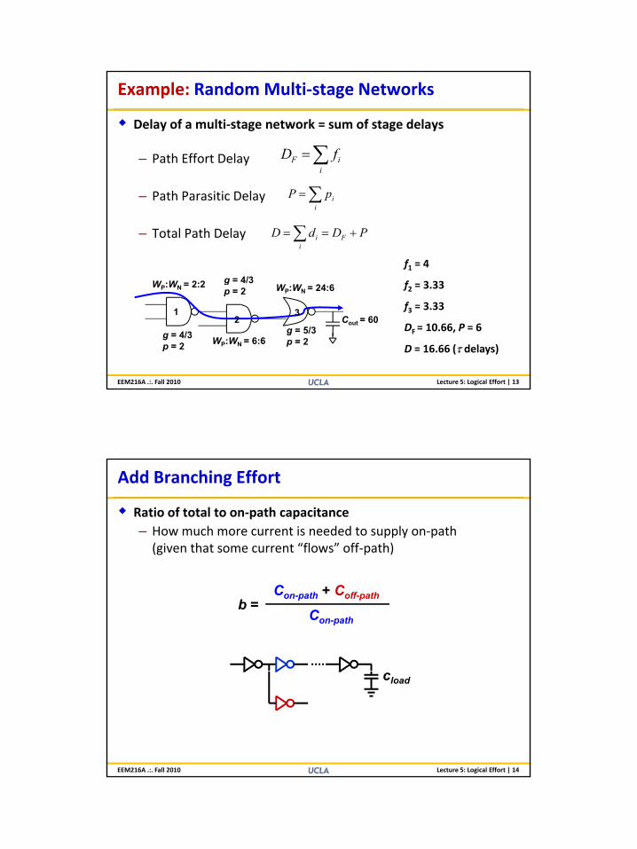
Branching Example #2
g = 4/3p = 2
Cout = 60Cin = 4
WP:WN = 2:2 WP:WN = 24:6
WP:WN = 6:6 WP:WN = 24:6
12
3
f1 = 8
f2 = 6.66
f1 = 4
f2 = 3.33
branching w/o bran.
For circuits with branching:– GPATH is the same = 3– HPATH is the same = 15– FPATH differs
g = 4/3p = 2
g = 5/3p = 2
Cout 60
WP:WN = 6:6
2f3 = 3.33 f3 = 3.33
D. Markovic / Slide 17
FPATH differs● h1 = 24/4= 6, h2 = 60/12=5, h3=2● FPATH = 4/3 · 6 · 4/3 · 5 · 5/3 · 2 = 177.8
F is no longer GH– New FPATH with branching: FPATH = G·B·H
EEM216A .:. Fall 2010 Lecture 5: Logical Effort | 17
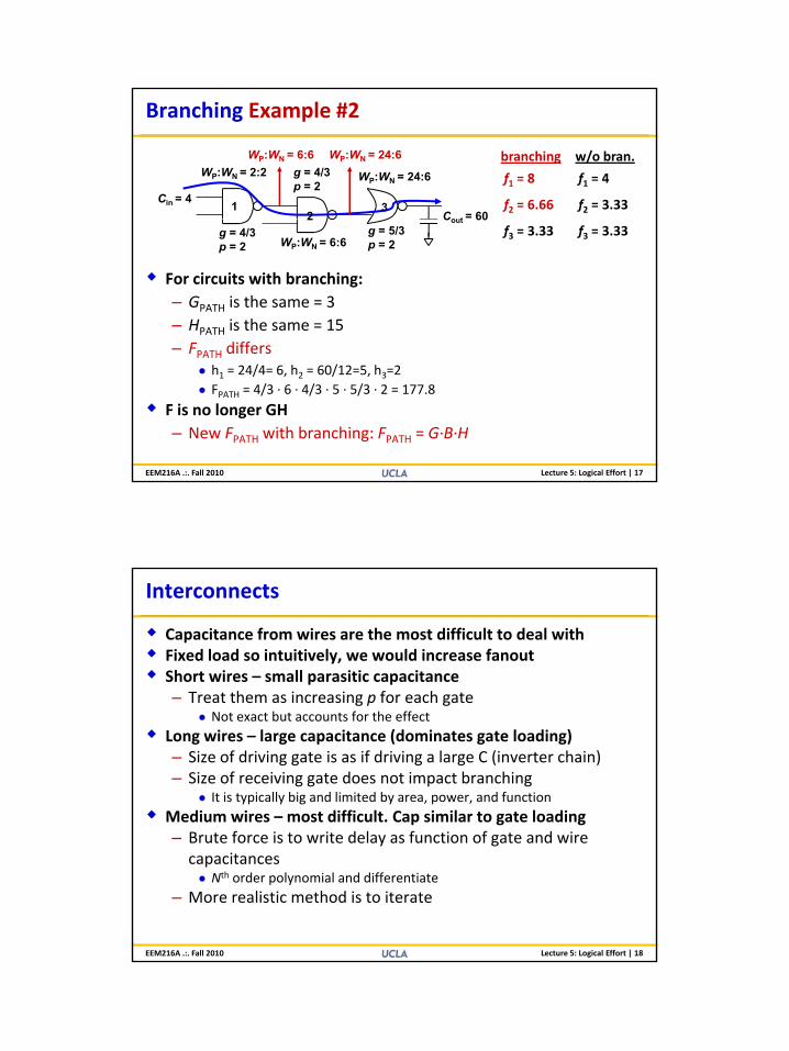
Interconnects
Capacitance from wires are the most difficult to deal withFixed load so intuitively, we would increase fanoutShort wires – small parasitic capacitance– Treat them as increasing p for each gateTreat them as increasing p for each gate
● Not exact but accounts for the effectLong wires – large capacitance (dominates gate loading)– Size of driving gate is as if driving a large C (inverter chain)– Size of receiving gate does not impact branching
● It is typically big and limited by area, power, and functionMedium wires – most difficult. Cap similar to gate loading
D. Markovic / Slide 18
– Brute force is to write delay as function of gate and wire capacitances ● Nth order polynomial and differentiate
– More realistic method is to iterate
EEM216A .:. Fall 2010 Lecture 5: Logical Effort | 18

10
Handling Wires & Fixed Loads
iCL
Cw
i
D. Markovic / Slide 19EEM216A .:. Fall 2010 Lecture 5: Logical Effort | 19
Summary
Delay and/or power of a logic network depend significantly on the relative sizes of logic gates (not transistors within a gate)Inverter buffering is a simple example of the analysis– The analysis leads to ~FO4 as being optimal fanout for drivingThe analysis leads to FO4 as being optimal fanout for driving
larger capacitive loadsTo generalize analysis of delay, we introduce logical effort– Delay normalized by inverter delay, d = g·h + p– g and p are characteristics of a logic gate that depends on its
structure and does not depend on gate size.● May have different g’s and p’s for different inputs and PU / PD
D. Markovic / Slide 20
● Simplify by using gAVG and ignoring C’s of intermediate nodes– Once a table of g’s and p’s are created for the catalog of gates,
delay can be calculated quickly and easilyNext we will look at how to size a network (instead of just analyzing it)
EEM216A .:. Fall 2010 Lecture 5: Logical Effort | 20

11
Optimum Effort per Stage
When each stage bears the same effort:
Fanout of each stage:
Complex gates should drive smaller load!!!
D. Markovic / Slide 21EEM216A .:. Fall 2010 Lecture 5: Logical Effort | 21
Minimum path delay
Gate Sizing Example (1/2)
From: David Harris
First, compute path effort:
Hpath
D. Markovic / Slide 22
The optimal stage effort is:
path
EEM216A .:. Fall 2010 Lecture 5: Logical Effort | 22

12
Gate Sizing Example (2/2)
We can now size the gates:
8.1345.1201 =⋅=z 5.14
45.135
=⋅=yx
D. Markovic / Slide 23
7.1245.13
4=⋅=
zy 1045.1
1 =⋅=xCin
The total normalized delay is (assuming pinv = 1):
EEM216A .:. Fall 2010 Lecture 5: Logical Effort | 23
Sizing Example with Branching
Size the gates for optimum delayOnce the path effort is determined, it is quite easy to determine the appropriate gate sizes
Start from the output of a pathiiout gC
C _=– Start from the output of a path– Work backwards to the input
● Check your work if the input is the same as the specification● Assuming each unit W has capacitance of unit C
optiin f
C _ =
g = 4/3Gate 2 (dup) Gate 3 (dup)
B = b1b2=4
F = 177.8, fopt = 5.62
D. Markovic / Slide 24EEM216A .:. Fall 2010 Lecture 5: Logical Effort | 24
g = 4/3p = 2
g 4/3p = 2
g = 5/3p = 2
Cout = 601
23Cin = 4
Cin3 = 60*5/3*1/5.6 = 17.9
Cin2 = b2*17.9*4/3*1/5.6 = 8.5
Cin1 = b1*8.5*4/3*1/5.6 = 4
WP3 = 4/5*17.9 = 14.3
WP2 = ½*8.5 = 4.25

13
Branches: Same # Stages, Different Loads
Example: 2 paths with the same # of stages but different loads– Optimal system has all paths with equal delay– Branching for path 1, b = 1 + α
A ti i th t ~● Assumption is that p1 ~ p2
Cout1
2
2222
1
1111
2211
1 2
in
out
in
out
NN
CCGBF
CCGBF
pFNpFN
DD
===
+=+
=Cin1
Path 1
D. Markovic / Slide 25EEM216A .:. Fall 2010 Lecture 5: Logical Effort | 25
Cout2
111
222
1
2
out
out
in
in
CGBCGB
CC
== αCin2
Path Effort Estimate
With equal‐stage branches, the Path Effort can be estimatedwithout knowing each stage’s, b– Htot = (Cout1+Cout2)/Cin (with B = 1)
Simple example for Path 1:– G = gNAND
– H1 = Cout1/Cin
– B = (1+Cout2/Cout1) ● Since F1 = F2 and G1 = G2, B = (1+Cout2/Cout1)
– F = G·H1·B = gNAND(Cout1+Cout2)/Cin
Cout1
Cout2
Cin1
Cin2
Path 1
Cin
D. Markovic / Slide 26
– Same as F = G·Htot
The errors occur with different g and p for the gates in the two different paths
EEM216A .:. Fall 2010 Lecture 5: Logical Effort | 26

14
Unequal‐Length Branches (Not Straightforward)
If both branches are long, then N1=N2 is an o.k. assumptionOtherwise, fopt differs between two paths
Solving precisely, example:C = H C
2dinv
1C1
– 2dinv − p = Cout1/C1
– (dinv − p)2 = Cout2/C2
– dnand = gnand(C1 + C2)/Cin
– D = dnand + 2dinv = gnand(Cout1/(2dinv − p) + Cout2 /(dinv − p)2) + 2dinv
– Take partial derivative of ∂D/∂(dinv)
Cout2
= H2·Cin
Cin = 1
Cout1 = H1·Cin
dinv dinvdnand 2
C2
D. Markovic / Slide 27
Not easy so ignore p to simplify– If gNAND = 4/3, H1 = H2 = 3: dnand= 2.35, dinv = 1.80– The per stage f = g·h (no p) is different per stage
Most branches are relatively long or not critical path
EEM216A .:. Fall 2010 Lecture 5: Logical Effort | 27
Re‐convergent Paths
Very similar to unequal branching, another logic structure that adds complexity to Logical Effort is recombined branches.– Typically constrains the sizing problem
Example: ignoring parasitics. Let x = Cin = 1– fa = (y+z)/x– fb = (3z/y)– fc = gNANDCout/z– 2 variables
Cout
Cinx
yz
fa
fb
fc2x NANDz
D. Markovic / Slide 28
– Constrain with fa = fb = fc, 2 vars equations (directly solve)● Any constraints are possible
– Increase variables by introducing more buffering (parallel to y)
EEM216A .:. Fall 2010 Lecture 5: Logical Effort | 28

15
Logic Opt. Example: 2‐Stage; 8‐Input AND
Assume symmetric 8‐input AND (β = µ =2, 3Wo is unit C)– gNAND=10/3, pNAND=8 for an 8‐input NAND– gINV = 1, pINV=1– Cout=100, Cin=1Cout 100, Cin 1
Logical effort– G = 10/3, B = 1, H = 100– F = 333.3– For 2 stages, fopt=18.3
● h2 = 18.3, Cin2 = 5.5, WP = 11Wo● h1 = 5.5, Cin1 = 1, WP = 0.6Wo
D l 36 6 9 45 6
x8
Cout
G1 G2
D. Markovic / Slide 29
● Delay = 36.6 + 9 = 45.6– Buffering
● For 3 stages, fopt = 7 (1 extra inverter), Delay = 31● For 4 stages, fopt = 4.3 (2 extra inverters), Delay = 28.2● For 5 stages, fopt = 3.19 (closer to optimal of 3.6), Delay=28● For 6 stages, fopt = 2.63 (below optimal of ~3.6), Delay=28.8
EEM216A .:. Fall 2010 Lecture 5: Logical Effort | 29
Logic Opt. Example: Multi‐2‐Input Gate 8‐AND
Many ways to implement this same function
Use a tree of fewer input AND gates– (A0A1)(A2A3)…– If multiple ANDs (as in a memory decoder), then partial
results can be shared
D. Markovic / Slide 30EEM216A .:. Fall 2010 Lecture 5: Logical Effort | 30

16
2‐input Implementation
Assuming that 3W has capacitance of unit C
out
Cout = 100
G7G6G5G4G3G2
Cin = 1
Assuming that 3Wo has capacitance of unit C– F = B·G·H = 4/33 ·100 = 235– fopt = 2.48 (too small)– D = 6·2.48 + 3·2 + 3·1 = 14.88 + 9 = 23.88
● Still better than 8‐input NANDOptimal sizing– G7: Cin7 = 100ginv/f = 40, WP=80W0
D. Markovic / Slide 31
– G6: Cin6 = Cin7gnand/f = 21.5, WP=32W0
– G5: Cin5 = Cin6ginv/f = 8.7, WP = 17.4W0
– G4: Cin4 = Cin5gnand/f = 4.7, WP = 7W0
– G3: Cin3 = Cin4ginv/f = 1.88, WP = 3.8W0
– Double check G2: Cin = Cin3gnand/f = 1, WP=1.5W0
EEM216A .:. Fall 2010 Lecture 5: Logical Effort | 31
4‐input Implementation
out
Cout = 100
G5G4G3G2
Cin = 1
Assuming that unit for C = 3Wo
– F = B·G·H = 4/3·6/3·100 = 266– fopt = 4.04 (a tad high)– D = 4·4.04 + 1·4 + 1·2 + 2·1 = 16 .:. 16 + 8 = 24.16
● Slightly worse than 2‐input! Due to self‐loadingOptimal sizing
D. Markovic / Slide 32
p g– G5: Cin5 = 100ginv/f = 24.75, WP=50W0
– G4: Cin4 = Cin5gnand/f = 8.16, WP=12.5W0
– G3: Cin3 = Cin4ginv/f = 2.02, WP=4W0
– Double check G2: Cin=Cin3gnand4/f = 1, WP=1.0W0
EEM216A .:. Fall 2010 Lecture 5: Logical Effort | 32

17
Example: 2‐NOR Implementation
i h i f
out
Cout = 100
G5G4G3
G2
Cin = 1
Assuming that unit for C = 3Wo
– F= BGH = 4/32*5/3*100 = 296– fopt = 4.14 (a tad high)– D = 4·4.14 + 3·2 + 1·1 = 16.56 + 7 = 23.6 (Best one!)
Optimal sizing– G5: Cin5= 100ginv/f = 24.1, WP=48W0
D. Markovic / Slide 33
5 5 0
– G4: Cin4 = Cin5gnand/f = 7.76, WP=11.6W0
– G3: Cin3 = Cin4gnor/f = 3.125, WP=7.5W0
– Double check G2: Cin = Cin3gnand/f = 1, WP = 1.5W0
Lesson: use close to optimal f, use gates with small p
EEM216A .:. Fall 2010 Lecture 5: Logical Effort | 33
Logical Effort “Design Flow”
Compute the path effort: Path Effort = F = ∏ g· h· b
Find the best number of stages: N* ~ log4(PathEffort)
Compute the stage effort: se* = (PathEffort)1/N
Working from either end, determine gate sizes:
D. Markovic / Slide 34EEM216A .:. Fall 2010 Lecture 5: Logical Effort | 34
Reference: Sutherland, Sproull, Harris, “Logical Effort,” (Morgan-Kaufmann 1999)

18
Summary of LE Design Methodology
1. Draw network2. Buffer non‐critical paths with minimum‐sized gates
• Minimize loading on critical path• Simplifies sizing of non‐critical pathSimplifies sizing of non critical path
3. Estimate total effort along each path (without branching)4. Verify that the number of stages is appropriate
• Add inverters if fopt > 55. Assign branch ratio of each branch
• Estimate based on the ratio of the Effort of the paths• Ignore paths that have little effect (i.e. min‐sized)
D. Markovic / Slide 35
• Include wire capacitances6. Compute delays for the design (include parasitic delay)
• Adjust branching ratios (especially with wire capacitance)• Repeat if necessary until delay meets specification
7. Re‐optimize logic network if fopt is small (Return to step 3)EEM216A .:. Fall 2010 Lecture 5: Logical Effort | 35