Embed Size (px)
Citation preview
MICROELECTRONIC & INFORMATION SCIENCES CENTER
Program Review 1985
Institute of Technology University of Minnesota
227 Lind Hall/207 Church Street SE Minneapolis, MN 55455 612/376-9122

tJ',S& t---\ se):.,
Prof. Wallace Lindemann, Director Dr. Martha G. Russell, Associate Director
Management Board
Dean E. F. Infante, Institute of Technology, Chair Prof. Robert Collins, Electrical Engineering Prof. H. Ted Davis, Chemical Engineering and Materials Science Prof. Robert Hexter, Chemistry Dean Robert Holt, Graduate School Mr. John Lacey*/Mr. Mike Schumacher, Control Data Corporation Prof. Wallace Lindemann, MEIS Assoc. Prof. Kurt Maly*/Prof. David Fox, Computer Science Vice President Rama Murthy, Academic Affairs Dr. Martha G. Russell, MEIS Dr. Gerald Dinneen*/Dr. William Sackett, Honeywell Mr. David Turcotte, Sperry Dr. Ennio Fatuzzo*!Dr. C.T. (Thomas) Walker, 3M
Technical Coordinating Committee
Prof. H. Ted Davis*/Prof. Wallace Lindemann, Chair Dr. Martha G. Russell, MEIS, Vice Chair Dr. William Sackett*/Dr. Don Boyd, Honeywell Dr. Krzysztof Burhardt, 3M Prof. Allen Goldman, Physics Prof. Richard Kain, Electrical Engineering Dr. Wall ace Lindemann* /Dr. James Key, Control Data Corporation Prof. James Slagle, Computer Science Mr. Larry Walker, Sperry Prof. John Weaver, Chemical Engineering and Materials Science
Executive Committee
Prof. H. Ted Davis, Chemical Engineering and Materials Science Department Head Prof. Robert Collins, Electrical Engineering Department Head Assoc. Prof. Kurt Maly*/Prof. David Fox, Computer Science Department Head
Fellowship Committee
Dr. Martha G. Russell, MEIS, Chair Asst. Prof. Wayne Gladfelter, Chemistry Prof. Marvin Marshak, Physics Prof. William Munro, Computer Science Prof. Allen Nussbaum, Electrical Engineering Prof. John Weaver, Chemical Engineering and Materials Science
* indicates previous member

Table of Contents
Executive Summary ................................................................... 1
Sponsorship ........................................................................... s
Perspectives From the University ...................................................... 7
Research ............................................................................. 11
Team Research Programs ........................................................ 13
Artificially Structured Materials for Microelectronics ................................ IS
High Performance Integrated Circuits ............................................. 23
III-V Compound Semiconductors and High Speed Devices ............................ 31
Intelligent Systems ............................................................ 39
Small Grants Program ........................................................... 51
Laboratory and Research Facilities ............................................... 53
Education ............................................................................ 59
Doctoral Fellowships ........................................................... 61
Faculty Development ........................................................... 67
Course Expansion .............................................................. 69
Technology Transfer ................................................................. 71
Videotaped Seminars ........................................................... 73
Technical Reports .............................................................. 75

Executive Summary
The university-industry partnership which initiated the Microelectronic and Information Sciences Center (MEIS) has grown into a network of over 200 scientists and engineers who conduct research in the fields of microelectronic and information sciences. Supported by industrial contributions and by the State of Minnesota, this technical community includes faculty, graduate students and industrial researchers.
MEIS is halfway through its first program cycle. This cycle is based on the 5-7 year period required to initiate new lines of research, prepare graduate students to assist in the conduct of that research, complete their dissertation and degree activities and move into the workplace. The products of MEIS programs include new knowledge disseminated through publications, new scientists with expertise in these new fields of knowledge, and intellectual vitality enhanced by stimulating collegial interactions.
The return on investment in MEIS is already visible. It can be seen in additional research funding leveraged for MEIS sponsored projects, published and presented research results, the addition of quality faculty members and graduate students, new and remodeled laboratory facilities, new courses, and the establishment of a research community.
To the $6 million of industrial contributions which initiated MEIS in 1980-81, the State of Minnesota has added $1.2 million in the 1983-85 biennium and $1.35 million in the 1985-87 biennium. These funds have helped attract over $10 million of outside support to the University for research in microelectronic and information sciences -- $2 million in 1983, $2 million in 1984, and $6 million in 1985.
The second half of this first program cycle will bring these research projects to fruition and begin the flow of approximately I 00 graduate scientists into the academic and industrial workplace. In the next 3-5 years, results of research activities now underway will be reported to the technical
community. Collaborative activities generated by these results will provide the scientific basis for the next cycle of MEIS research programs. The community of researchers will expand to include alumni and new students, and this expanded interaction will continue to strengthen the MEIS partnership.
The MEIS program cycle, shown graphically on the following page, is a continuous building of cooperative university-industry interaction resulting in advancement of microelectronic and information sciences research and education at the University of Minnesota and at member companies.
During this first program cycle, MEIS has focused on four fundamental team research programs:
• Artificially Structured Materials for Microelectronics
• High Performance Integrated Circuits
• III-V Compound Semiconductors and High Speed Devices
• Intelligent Systems
These research programs were chosen because they bridge the intellectual strengths at the University of Minnesota, the research interests of our corporate sponsors, and the demand for well-educated scientific personnel. Faculty expertise in these areas provides a continuing source of able consultants for industry. This consultation provides industry with early access to new ideas and provides faculty with insights into the technological concerns of industry. Graduate students provide a source of innovative ideas and assistance for faculty and also establish links between faculty and industry researchers through their summer jobs and eventual employment.
In the next five years, about 100 M.S. and Ph.D.

MEIS PROGRAM CYCLE 5-7 YEARS
COOPERATIVE ~ RES. PROJECTS
'/ INFORMATION ....... TRANSFER
81 - 83 83- 85
2
GRADUATE STUDENTS WORK
SUMMER IN INDUSTRY
85- 87

scientists who have been part of MEIS related research will have graduated and will be contributing their analytical skills to current problems in the microelectronic and information sciences. These students are being educated through research programs sponsored directly or indirectly by MEIS and through departmental programs which have been facilitated by new courses, new faculty, and new and remodeled laboratories.
The development of the MEIS research community has resulted from the involvement of people from seven departments at the University of Minnesota, and of our MEIS member companies -Control Data, Honeywell, Sperry, 3M, ADC Telecommunications, Cray, VTC, and Zycad.
Representatives from these companies have participated in all phases of the program cycle, from giving input for research directions to interacting with graduate students and reviewing research projects.
This involvement strengthens the University of Minnesota's research activities through exposure to state-of-the-art instrumentation and through the commitment to success encouraged by teamwork. This interaction augments member companies' own in-house research activities by giving their employees a chance to collaborate with scientific peers and to recruit outstanding graduate stu-
3
dents. Other partnership benefits to members of MEIS include early access to intellectual breakthroughs, opportunities for continuing education, research interaction, recruiting assistance, tax advantages and increased recognition on campus.
Continuing industrial support and additional federal research support for the second half of this first program cycle are being sought. Continued development of the Microelectronic and Information Sciences Center's programs will depend on the research partnerships now underway and on sustained support from member companies, the State of Minnesota and the University of Minnesota. This partnership is vital to the Minnesota research community.
Minnesota scientists are an enormous resource. By strengthening their research base, by increasing their numbers, and by building collaboration among them, MEIS increases the benefits of these intellectual resources to the entire research community.
Martha G. Russell, Ph.D. Associate Director

Sponsorship
Throughout its program cycle, MEIS has benefited from the sponsorship and active participation of member companies. Ongoing growth of the MEIS Center's physical, organizational and scientific aspects is a result of involvement by scientists and engineers from member companies.
MEIS offers important advantages to sponsors seeking collaborative opportunities in the microelectronic and information sciences research and education. Most important is the opportunity to participate in the development and direction of research and educational programs at the University of Minnesota.
Sponsors participate in MEIS Management Board deliberations. This alliance of industry and University representatives recommends program policy and research directions for MEIS. Scientists and engineers from sponsoring companies participate in research programs.
In addition to shaping education and research goals, member companies have early access to new knowledge on the cutting edge of the microelectronic and information sciences in the form of technical reports, workshops and symposia. Seminars and the videotapes made from them provide new technological information via lecturers and researchers from other academic, industry and government organizations.
The member companies are committed to this MEIS educational, research and technology transfer mission. Many of these industrial sponsors maintain corporate headquarters in the Twin Cities.
In addition to the support of corporate sponsors, MEIS is supported by the State of Minnesota and federal grants and contracts. The cooperation of these industrial, university, and governmental organizations enhances the development of MEIS as a leading center for research and education in microelectronic and information sciences.
5
Major Sponsors
MEIS was established through the initial sponsorship of four multinational corporations dedicated to the advancement of science and engineering in a joint venture with the University's Institute of Technology.
Control Data Corporation is based in the Twin Cities suburb of Bloomington and has its major research facilities in the Twin Cities area. Control Data has been a strong supporter of collaborative research organizations and an advocate of university-industrial partnerships. Control Data's products serve the areas of computingrelated hardware and computing-enhanced services, including computation, information, education, and finance.
Honeywell Inc. has its headquarters in Minneapolis and has numerous research and development centers in the Twin Cities metropolitan area. Honeywell is a leader in the areas of automation and control through its integration of computer, control, and communications technologies. Honeywell is a major supplier of integrated information and control systems for manufacturing and building automation.
Sperry Corporation has numerous research and development branches in Eagan and Roseville and other Twin Cities suburbs. These include the Semiconductor Operations, Knowledge Systems, and System Products Division as well as the headquarters for the Defense Products Group. Sperry recently increased its emphasis on electronics, with a coordinated long-term commitment to research and development in specific electronics fields and systems integration.
3M has its corporate headquarters in St. Paul and has extensive research and development activities throughout the Twin Cities area. 3M is comprised of four sectors with a global market for: tapes, adhesives and abrasives; health and personal safety products and services; graphic, audiovisual and advertising products; and elec-

tronic, telecommunications, information processing and recording products.
Associate Sponsors
The Associate Sponsorship category was approved by the MEIS Management Board in 1985 to encourage the active participation of smaller companies with more specific research interests in microelectronic and information sciences. Four companies have already taken advantage of the opportunity to become involved in MEIS as Associate Sponsors.
ADC Telecommunications, Inc. is located in the Twin Cities suburb of Bloomington where its major research and development facilities are based. ADC Telecommunications designs, manufactures and sells diverse electromechanical and electronic products for the telecommunications industry.
Cray Research, Inc. is a leading producer of supercomputer hardware and software. Cray has
6
committed over 100 million dollars to the design of supercomputers over the past four years. The company is best identified with CRA Y -1 , CRA Y X-MP, and CRA Y-2 computers. Cray' s corporate headquarters are in Minneapolis with its major software research facilities in the Twin Cities suburb of Mendota Heights and advanced research and development facilities in Chippewa Falls, Wisconsin.
VTC Incorporated is based in the suburb of Bloomington. VTC's two divisions design and market high performance semiconductor devices. The VHSIC Technology Division specializes in high-speed CMOS logic and radiation hardened devices. The Microcircuits Division manufactures mainly bipolar devices.
Zycad Corporation is located in the Twin Cities suburb of Arden Hills. Zycad designs, manufactures and markets high-performance special purpose processors used to increase engineering productivity in the design and development of complex integrated circuits and electronic systems.

Perspectives From the University
From the Institute of Technology
Investments in the Microelectronic and Infonnation Sciences Center (MEIS) are paying off significantly. MEIS programs have had a major impact in the Institute of Technology through strengthening existing programs and initiating new directions for research and education. Numerous recent developments in the Institute of Technology have been possible because of additional departmental strengths developed with resources from MEIS.
MEIS is now joined in its research, education and infonnation transfer missions by the Supercomputer Institute, the Productivity Center, and other interdepartmental centers and research programs. These exist because of the model established by MEIS for industry-universitygovernment cooperation. In addition, many of these other research and educational activities have been based on activities which received their strong initial push from MEIS. For example, the large grant recently received by faculty in the Department of Computer Science recognizes the strength in high perfonnance computing in that department. This strength would not have existed without the investments made by MEIS in faculty research programs.
The University of Minnesota is constructing a new building for the Departments of Electrical Engineering and Computer Science. This new facility will be the home for a substantial number of research activities at the center of the charter of MEIS. This building will serve as the flagship for the implementation of the ten year facilities plan of the Institute of Technology. Programs of MEIS are a very high priority in this plan.
Prof. E. F. Infante, Dean
7
From the Graduate School
Although MEIS has been in existence for only a brief time, it has already made major contributions to the efforts by the Graduate School to provide high quality educational programs for graduate students and to promote excellence in research and scholarship by University of Minnesota faculty and students. These contributions will certainly grow as MEIS pursues its program cycle over the next 3-5 years and beyond.
Several of the MEIS activities have had particular significance for the Graduate School. Some are more directly related to graduate education. First, MEIS has made a special effort to attract graduate students by emphasizing a multidisciplinary, interdepartmental approach to graduate programs. Such an approach coincides with and reinforces Graduate School efforts to encourage interdisciplinary study and research. Second, the recruiting and promotional mechanisms used by MEIS serve as useful models for other programs which have been less successful in obtaining students. Third, funding for interdepartmental programs from conventional University sources is still limited and thus the MEIS fellowship program fills an important gap while stimulating interactions among disciplines. By bringing in industry funds, MEIS widens the financial base for graduate student support in general, which is especially important in this time of increased costs of graduate education.
Other activities are more related to the stimulation of research by faculty, as well as students. First, through its sponsors and contacts, MEIS provides continual input concerning new and projected basic research needs of industry. This input keeps the faculty and students current and offers a direct avenue for application of findings. Second, the small grant funds administered by
MEIS complement Graduate School support for faculty research, thus expanding the resources available to set up new faculty and to act as seed money for new research projects. Third, by encouraging and supporting use of various University-wide facilities, such as the Surface Analysis and Electron Microscope units in the Shepherd Labs, MEIS increases their visibility and helps them maintain a stable funding base.
Clearly, MEIS and the Graduate School share many goals. Their continued and expanded interactions will certainly lead to further increase in the quantity and quality of research and graduate training in technology at the University of Minnesota.
Prof. Robert T. Holt, Dean
From the Department of Chemical Engineering and Materials Science
The Department of Chemical Engineering and Materials Science has profited substantially from the existence of MEIS, and many of our faculty play central roles in the Center. Interests of the Department, as reflected by our faculty, overlap to a significant degree with those of MEIS. These range from the chemical engineering aspects of microelectronic processes, to the development of new materials for devices, to the understanding of adhesion in polymer photoresists.
Since 1982 when we made the decision to establish a microelectronic materials thrust, MEIS has helped the Department to attract key professors who have provided the "physics flavor'' for materials research at Minnesota. Over the past three years, these faculty members have been highly successful in establishing showcase laboratories for the Department, the University, and MEIS. In addition, the MEIS-sponsored synchrotron radiation beamline project provided us with a very attractive dowery for a new faculty member.
In 1983 an MEIS-sponsored visiting professor and a professor in our Department created, with MEIS support, a very successful course which focuses on microelectronic processing in device
8
fabrication. They have since been preparing a text on the subject.
Several faculty members in the Department are active in two of the team research programs which receive direct research assistance from MEIS. Additional MEIS support for the faculty of Chemical Engineering and Materials Science has been awarded through the small grants program.
The clear overlap between the interests of the faculty of the Department and MEIS has helped us to establish new research areas within the University of Minnesota and to strengthen our already strong position in chemical engineering and materials science.
Prof. H. Ted Davis, Head
From the Department of Chemistry
The emergence of MEIS as a focal point and impetus for research and teaching in microelectronics has been of substantial benefit to the Department of Chemistry. MEIS has brought the significant problems of microelectronics to the chemists' attention and has encouraged them to get involved in solving these problems.
The chemists who are involved in the Artificially Structured Materials program have now been able to expand their research activities into areas of importance for microelectronics. This has broadened the knowledge and expertise in this area, generated new ideas, and encouraged more activity in the general area of electronic materials. These faculty and the students provide a new knowledge base and personnel base for the future.
Of particular importance to chemists have been the faculty seminars involving physicists, chemists, materials scientists and engineers, and the symposium on "Organic Chemistry and Microelectronics." These seminars have brought together researchers who otherwise would not communicate with each other and served to stimulate a number of innovative ideas.
Of more obvious importance is the seed money

provided for new projects in microelectronics. These grants have allowed each investigator to initiate a project which would otherwise not exist. All of the investigators have ongoing research programs and these would continue without MEIS. The difference is that the seed money has attracted their attention and efforts to new projects in the microelectronic sciences.
Prof. Larry L. Miller, Chairman
From the Department of Computer Science
The interaction between MEIS and the Department of Computer Science has created positive growth in computer science education and research. MEIS has funded the development of a number of new courses in the areas of artificial intelligence and VLSI design. Many of these courses are offered via the University of Minnesota's University-Industry Television for Education (UNITE) system thereby expanding the continuing education offerings of the Department.
MEIS has also helped in the addition of faculty and funds for their research to enable fast startup research. Contributions by MEIS have included the sponsoring of the Intelligent Systems program and providing a $125,000 seed grant to a research team in 1982-83. A subgroup of that team submitted and has received an award of $3.75 million from the National Science Foundation for high performance computing research. The Department of Computer Science now has two large, self-sustaining laboratories which have won national acclaim for their significant contribution in the research community.
Assoc. Prof. Kurt J. Maly, Head
From the Department of Electrical Engineering
The Department of Electrical Engineering has benefited from the cooperation and support of MEIS through its impact on many of our programs. Participation in the MEIS-supported VLSI facility has allowed Electrical Engineering
9
faculty to offer courses in the computer-aided design of VLSI circuits. Many of the students are employed in local industry and it is essential for them to improve their professional skills by such courses. MEIS support for course development has greatly enhanced the ability of the Department to maintain research in this field.
Another important aspect of the cooperation between the Department of Electrical Engineering and MEIS has been the support offered to the Microelectronics Laboratory. Support has been provided by MEIS as a grant to aid in modification of the existing building and the initial installation of the clean room facilities, as well as maintenance of the laboratory for research and teaching. Continued support of the research activities conducted in this laboratory will aid the ability of the Department to train graduate and undergraduate students in this important area of technology.
The support offered to faculty members in two of the team research programs has helped shape the graduate program within the Department. The active partiCipation in these programs has changed the character of the Department in a very positive way.
In the year to come, the cooperation with MEIS is expected to greatly enhance the ability of the Department to attract senior faculty in the area of microelectronics. With the completion and activation of the new clean room facilities and the related construction of a new Electrical Engineering and Computer Science building, the continued support of MEIS will be an added asset in the ability of our department to recruit faculty.
Prof. Robert J. Collins, Head
From the School of Physics and Astronomy
MEIS has had an impact on both the research and teaching programs of the School of Physics and Astronomy. In the case of the teaching program, the development of courses in solid-state physics had taken place years before the founding of MEIS. Funds from MEIS were used,

however, to help support the development of a course in use of Monte Carlo and other computation techniques in physics.
The research programs of the faculty of the School have been assisted both through the Small Grants program and a seed grant program which evolved into the Artificially Structured Materials for Microelectronics program. Participation in these programs has helped to foster university-
10
industry cooperation, and has made the members of the Physics faculty more aware of the opportunities for interdisciplinary and multidisciplinary research. The support of the School by MEIS has greatly assisted in establishing the research programs of the younger faculty, as well as in augmenting the programs of more senior faculty.
Prof. Charles F. Campbell, Head
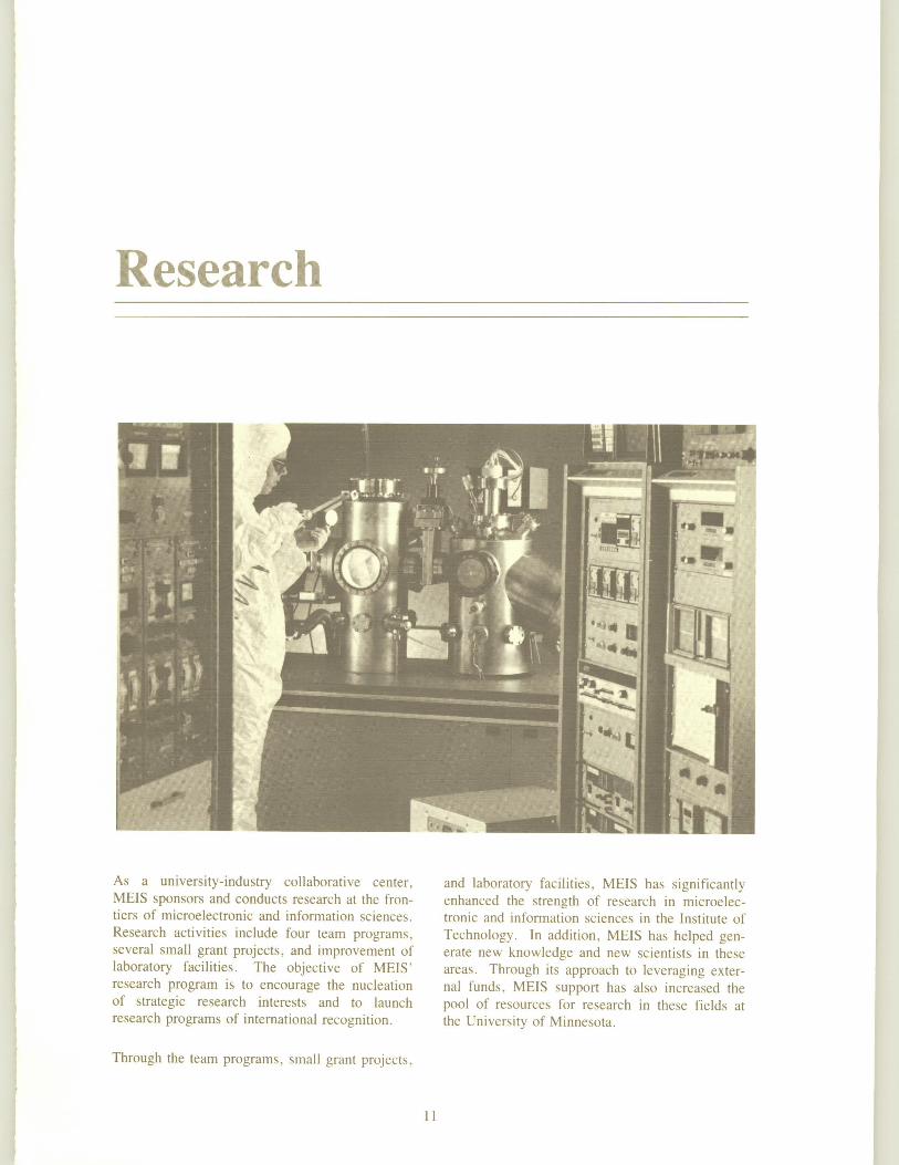
Research
As a university-industry collaborative center, MEIS sponsors and conducts research at the frontiers of microelectronic and information sciences . Research activities include four team programs , several small grant projects , and improvement of laboratory facilities . The objective of MEIS' research program is to encourage the nucleation of strategic research interests and to launch research programs of international recognition .
Through the team programs, small grant projects ,
11
and laboratory facilities, MEIS has significantly enhanced the strength of research in microelectronic and information sciences in the Institute of Technology . In addition, MEIS has helped generate new knowledge and new scientists in these areas . Through its approach to leveraging external funds, MEIS support has also increased the pool of resources for research in these fields at the University of Minnesota.

Team Research Programs
MEIS sponsors four team research programs. The purposes of these programs are: (1) to stage carefully coordinated attacks on cutting edge problems which are long ranged and have high potential for practical payoffs; (2) to leverage additional funding to these important areas; and (3) to prepare new scientists with the analytical, creative and disciplined approaches needed in the future to solve problems.
The team programs accomplish this by bridging several disciplinary perspectives, by incorporating dissertation activities of graduate students, and by actively interfacing with industrial scientists and engineers.
These team research programs were initiated by MEIS in I982 with a call for proposals to University of Minnesota faculty to establish research teams in the microelectronic and information sciences. Proposals were reviewed by technical experts at the University of Minnesota and at participating companies. MEIS selected four team programs from the projects which had received seed monies in I982-83 plus several new proposals submitted during a second round in I983-84.
I3
The criteria for selection included consistency with collaboratively identified University and corporate research objectives, technical merit, strength of intellectual expertise, interdisciplinary synergy, and probable ability to generate additional research funding. Team research programs are required to match MEIS funds on at least a I: I basis.
MEIS team research programs are:
• Artificially Structured Materials for Microelectronics
• High Performance Integrated Circuits
• Ill-Y Compound Semiconductors and High Speed Devices
• Intelligent Systems
Each program holds an annual review to describe results of research conducted, provide access to those results for the technical community, and invite input regarding future directions and funding.

Artificially Structured Materials for Microelectronics
This program is a coordinated effort at synthesizing new electronic, magnetic, and optical materials using both physical and chemical techniques. The purpose of the work is to develop new types of small structures and to investigate their properties.
The emphasis is on basic research on systems which have structures and compositions which are unlike those of natural materials in thermodynamic equilibrium, and in which the synthesis involves control of both composition and structure over atomic distances. The effort combines investigations using the methods of materials science, chemistry, and condensed matter physics.
Research is focused on the crucial issues in artificially structured materials research: the development of better ways to fabricate and characterize materials, and the study of the unique properties they have due to their unusual structure.
Research has demonstrated that through the study of new materials, the discovery of new and unanticipated physical phenomena is almost inevitable. These discoveries have been, and will continue to be, the wellspring of new types of electronic devices.
The physics of small structures, or coupled small structures, goes beyond that of single crystals or natural surfaces. It is a field of study between bulk solids and isolated atoms and molecules. A large variety of structures can be fabricated. Examples are layers, channels, tubes, networks, islands, and blocks. The structures can be binary, ternary, or higher order structures. They can be epitaxial interfaces or can be compositionally modulated amorphous or polycrystalline entities.
Periodic epitaxial structures can be viewed as
15
artificial crystals. Structuring can involve materials of one general type or result from the juxtapositioning of materials of widely different types. The physical properties of structures depend upon whether their geometric scales are larger than, comparable to, or much smaller than certain characteristic length scales such as atomic spacings, electronic wavelengths, mean free paths, Debye lengths or the coherence lengths for the order parameter of an ordered phase such as ferromagnetism or superconductivity.
The work described here has been divided into two complementary sections which are directed at the study of the fundamental building blocks of artificially structured materials. The first section describes the fabrication and characterization of novel thin film structures, small particle structures and coupled small structures using physical vapor deposition techniques, as well as chemical techniques, which have not been used previously in the preparation of microelectronic materials.
The second section discusses the study of the electronic, magnetic and optical properties of the structures to be produced and characterized by the techniques and procedures discussed in the first section. The study of simple thin film and small particle systems should precede the study of more elaborate multilayer or superlattice configurations. The idea is to develop the expertise for future expansion into the investigation of more elaborate artificial structures.
Fabrication and Characterization
Fabrication and characterization research IS
divided into two main areas. The first to be described involves interfacial growth and structure of ultra-small composites.

Interfacial Growth and Structure of Ultra-Small Composites
Progress
Four areas of progress consist of (i) processing technology for laying down structures, (ii) transmission electron microscopy (TEM) techniques for examination of interfaces, (iii) scanning electron microscopy (SEM) techniques for characterizing defect densities, and (iv) preparation of interfaces with variable defect densities.
The processing technology area involves sputter deposition techniques for titanium/molybdenum modulated structures so that the phase transition behavior (the omega transition) can be better characterized.
The TEM techniques area is concerned with developing single jet-polishing in conjunction with chemical etching or ion-milling techniques to prepare metal/metal, metal/semiconductor or metal/oxide interfaces for TEM. An electron channeling technique which provides both crystallographic and defect density information with back-scattering electrons (BSE) from the nearsurface is being developed.
Members of the team have also been examining the evolution of structures of Ni films on Si02,
the stability of submicron stripes (wires) of Ni and Pt on Si0
2 using electron-beam lithography.
Two students have been participating in a senior design project to provide thermal cycling of Al!Si of Al-Cu/Si interfaces. Another student examined microstructures of metal films (Cu, Ni, Cr) on Si after Xe ion implantation using SEM, SAM, and XPS with sputter depth profiling. In the latter, films were prepared by scientists in the Advanced Technology Group at 3M who have excellent facilities for film growth and ion implantation.
Theoretical research on the nucleation and growth of order in systems driven far from equilibrium has also been carried out. Results on the growth of order have been obtained for several kinetic Ising models. The behavior of thin superfluid films, with emphasis on finite size effects, has also been investigated, particularly in connection with the quantum size effect studies carried out on thin metal films.
16
Planned Work
Future plans include the use of BSE techniques for probing interface defect structures, such as dislocation structures which may be produced by low temperature thermal cycling or mechanical cycling and precipitate phase defects, and verified with standard TEM techniques.
The study of the evolution of microstructures and stabilities of Ni wires and particles on Si0
2 or Si
will continue using high resolution TEM, SEM, and elemental analysis. The team anticipates that it will take several months to perfect the electron-beam lithography techniques to submicron structures, and the goal is to push this technique to 100 angstrom widths. The possibility of trapping the wires in the metastable wire state without breakup into particles will provide a· method of making wires much narrower than can be currently obtained using direct lithography.
Formation and stability of interfacial silicides of these materials will also be examined. The use of parallel stripes will permit examination of two-dimensional diffusion processes at the edges of metal wires. High resolution electron microscopy should yield the shapes of these structures down to almost atomic resolution.
The collaborative program with 3M will continue by examining the properties of vacuum and sputter deposited metal and compound films.
In the theoretical area, the team will continue to investigate the behavior of systems after they have been driven very far from equilibrium by a sudden change in the thermodynamic parameters and fields.
The influence of the following variables on the growth of order will be investigated: the presence of vacancies and defects, atomic concentrations, substrate structure, quenching rates, equilibrium lattice structure, and magnetic fields.
Future plans include extending theoretical techniques to models with non-stochastic dynamics, and to study the reasons for the formation of specific crystal structures from the melt.

Novel Fabrication and Characterization of Small Structures on Surfaces
The second area within fabrication and characterization of artificially structured materials involves novel fabrication and characterization of small structures on surfaces.
Progress
Significant progress has been made in the development of fabrication strategies based on chemistry initiated by low energy collisions between charged particles and reactive surface species. The vacuum system which is used to study plasma sheath chemistry has been completed and brought into service in studying plasma deposition of styrene and the plasma etching of hydrocarbon polymer thin films.
In both systems the unique physical environment of the sheath has been shown to allow access to ion-molecule reaction channels which are not followed in the corresponding thermal reactions. That is, the existence of the sheath allows for unique chemistry due to the acceleration of the ions in the sheath where they may undergo collisions with gas phase and surface species. For example, the team has observed the predominance of phenylacetylene cation radical chemistry in plasma reactions which lead to dimer and polymer formation in the vicinity of and on the surface at which plasma-deposited styrene polymer films are forming. This chemistry is not observed in thermal ion-molecule reactions which occur when styrene cation radical is formed by low energy electron impact at high pressures of styrene.
The second area of progress has been the design and construction of a coincident beam apparatus. The system became operational during the summer of 1985.
Another area of activity is the use of solid state organic synthesis to produce three dimensional molecular structures on surfaces. Progress has been made on producing large molecular building blocks and developing linking reactions.
Excellent samples for X-ray contact have been made available. A postdoctoral researcher has become an expert in electron microscopy. During the winter all of the new membrane samples
17
were completely recorded using electron microscopy. The team is awaiting the Brookhaven storage ring to come on line again, and IS
scheduled to use it beginning this summer.
Planned Work
The work on charged particle chemistry in the next year will involve investigating the role of low energy ion and electron bombardment of surfaces on which reactive precursors to film formation are absorbed.
Actual surface synthesis using oriented chemistry will commence in the next year. This phase of the activity has had to await the arrival of a postdoc with training in synthesis.
In the study of X-ray contact microscopy, the team will use approximately five weeks of synchrotron time over the next six months, and an equal amount of time in the following six months, mapping calcium in a large variety of striated muscle specimens. Having demonstrated that calcium can be mapped at the 100 Angstrom resolution level, the principal task will be to use this extraordinary tool and discover what the active site of muscle protein is that binds calcium.
In addition to being a very significant biological problem, it will serve to establish the technique of X-ray microscopy as the pre-eminent elemental mapping technique with the highest spatial resolution. The next step will be to transfer the application of this technique to materials of importance in microelectronics.
Electronic, Magnetic and Optical Properties of Small Structures
The second major area of research involves the study of electronic, magnetic and optical properties of small structures.
Progress
Work in this area has been concerned with the properties of ultra-thin films, the investigation of the properties of single interface GaAs/ AlGaAs heterostructures, and the theory of the electronic properties of heterostructures and ultra-thin films. In addition, theoretical and experimental studies

of nonlinear optical properties of thin films have been developed.
Research on ultra-thin films has been focused on the properties of a metal film at the threshold of electrical continuity and slightly beyond. Major progress was made with the successful comissioning of an apparatus which permits ultra-high vacuum growth of thin films using MBE techniques, analysis using scanning Auger spectroscopy, reflection electron diffraction studies, and in-situ electrical measurement at low temperatures. A study of the thickness-dependence of the properties of thin tin films, which was initiated for the purpose of testing the apparatus, has resulted in several unusual discoveries. In this instance the study of superconductivity is a very sensitive probe of the properties of the film at various stages of growth.
The team has identified the onset of conduction as a very sensitive probe of the properties of the film at various stages of growth. Team members have identifed the onset of conduction as a percolation process, but one which appears to be fundamentally quantum mechanical rather than classical. Studies of ordinary metallic systems do not permit this distinction to be made easily.
Other aspects of the work have involved the study of the temperature dependence of the precursive electrical conductivity above the superconducting transition temperature. These measurements can be used to probe models of electron dynamics in a disordered film. To facilitate the comparison of experiment and theory, the team has undertaken the study of artificial random materials which are being prepared using electron beam lithography. The purpose is to compare the results of measurements on real random systems and these model systems with the theoretical predictions.
A study of the thermoelectric properties of single interface GaAs/AIGaAs heterostructures has been completed providing the first thermodynamic information on the quantum Hall effect in single interface 20 electron systems. Research also indicates that thermopower measurements may be extremely valuable for understanding mobility limits in heterostructures.
Theoretical work on the electronic properties of
18
artificially structured materials includes studies of the effects of dimensional constraint, as well as the impact of unusual structural environments for the electrons.
The present focus is on the theory of the Anomalous Quantum Hall Effect which has been discovered experimentally in heterojunctions. The anomalies in this important discovery occur at fractionally occupied Landau levels. This is a cooperative phenomenon similar to superconductivity. Present work is on the elucidation of the energetics of this effect, particularly why certain well-defined fractions are preferred over others. Progress to date has included a demonstration that the simplest of these states occurs when the charge density is at precise values which permit local screening of the charges in such a way that the density is constant.
Planned Work
Research on superconductivity at the connectivity threshold will continue with emphasis shifting to the study of amorphous materials which are continuous when they are very thin and to the study of epitaxially grown AI films. Structural studies of film growth will be pursued using both Auger analysis to investigate substrate coverage and transmission electron microscopy to determine microstructure.
The study of models of random systems produced using electron beam lithography will be fully developed. Electrical measurements and magnetic susceptibility studies will be performed with a superconducting susceptometer. Future research will also examine electrical and magnetic properties of ultra-thin wires, threshold conditions for ferromagnetism in very thin films, and studies to provide information on the limits of mobility in devices based on GaAs/ AIGaAs technology.
There is a strong synergism between the above experimental work and theoretical work on the Anomalous Quantum Hall Effect. A theoretical formalism will be developed to investigate a model in which there is a condensed state of excitations, where the excitations are topological excitations similar to vortices and interacting via a 20 Coulomb-like interaction which is locally screened at specific densities.

• l I i
I
Investigators
P. F. Barbara, Assistant Professor of Chemistry and Chemical Physics, presently supervises a group of eight graduate students working on different aspects of molecular photophysics. He has authored 15 refereed publications. His research interests are in ultrafast chemical and physical phenomena of molecular substances as probed by time resolved (picosecond) laser spectroscopy. Professor Barbara's research group recently developed a new approach to picosecond spectroscopy that allows the detection of extraordinary subtle photophysical effects. He is presently an Alfred P. Sloan fellow and Presidential Young Investigator.
C. E. Campbell, Professor of Physics and Head, School of Physics and Astronomy, is a manybody theorist with a research program during the last eleven years at the University of Minnesota focusing primarily on the microscopic structure of quantum fluids and adsorbed systems. This program has been sponsored continuously by the National Science Foundation during this period, and usually consists of one post-doctoral research associate and one to three students, as well as substantial international collaboration with other physicists. Approximately 40 refereed publications and numerous invited papers have come out of this program, as well as involvement in the organization of a number of major international conferences and workshops. Most recently the research focus has been expanded to include the study of correlation effects in electronic systems.
E. D. Dahlberg, Assistant Professor of Physics, directs a research group consisting of seven graduate students. His present research interests primarily involve the experimental study of the effects of dimensional constraints and disorder on the electric and magnetic properties of metals. The studies involve measurements of the magnetoresistance, thermoelectric effect, specific heat, magnetization and magnetic susceptibility. He presently has authored 20 refereed publications. He is currently an Alfred P. Sloan fellow.
John F. Evans, Associate Professor of Chemistry, is presently engaged in research relating to the preparation and characterization of thin films with unusual properties. Within the context of these studies Professor Evans and his group are involved in the use of nonequilibrium plasma
19
chemistry for the fabrication of modified electrodes and for the etching of polymer overlays on metal/metal oxide composites. The chemistry and physics of low energy ( 10-1000 e V) ion and electron bombardment of reactive or bound species resident on solid surfaces is under study with regard to the involvement of such processes in the plasma surface interactions associated with the deposition or etching of surface films. Professor Evans supervises a group of fourteen graduate students and one postdoctoral research associate. He was recently awarded an Alfred P. Sloan Foundation fellowship for the period 1983-85.
William W. Gerberich, Professor of Materials Science, received a B.S. from Case-Western University and an M.S. at Syracuse University before working in the Aerospace Industry from 1959-1967, including JPL at Cal Tech. He subsequently returned to academia through Lawrence Berkeley in 1971. Since then he has been with the Department of Chemical Engineering and Materials Science and is currently Associate Head. His research program centers on the physical and mechanical characterization of solids and interfaces with special reference to fracture. This has resulted in 44 M.S. and Ph.D. degrees and approximately 140 published papers and book chapters, mostly with his students. He won the William Sparagen Award of the American Welding Society for the best research paper in 1968 and is currently on the Board of Review and Board of Publications of Metallurgical Transactions, ASM International Metals Reviews and Acta Metallurgical. His research program currently has six graduate students and commitments from DOE and NSF over the next three years.
Allen M. Goldman, Professor of Physics, is Coordinator of the Artificially Structured Materials for Microelectronics program. He presently supervises a group of seven graduate students and two research associates working on a number of experimental problems relating to thin films and tunneling junctions. He has authored more than 91 refereed publications and is the co-editor of a book on percolation, localization and superconductivity which has been published by Plenum Press. His research interests are primarily in the physics of superconductivity and magnetism with an emphasis on the effects of disorder and dimensional constraints on such systems and

the use of electron tunneling as a probe. Professor Goldman was a pioneer in the investigation of the Josephson effect and in the use of surface analytical techniques in superconducting materials research. He is a fellow of the American Association for the Advancement of Science and the American Physical Society and was an Alfred P. Sloan Foundation Fellow 1966-70.
Robert M. Dexter, Professor of Physical Chemistry, presently supervises a group consisting of a graduate student, a research associate, and a senior scientist working in two areas: surfaceenhanced Raman spectroscopy and x-ray microscopy. He has authored more than 45 refereed publications and is co-author of a monograph on molecular vibrations in crystals. His research interests have been in molecular spectroscopy with emphasis on vibrational and electronic spectroscopy of molecular crystals at low temperatures, rapid scanning infrared spectroscopy, Raman spectroscopy and x-ray absorption spectroscopy. Professor Hexter is known for first introducing the concepts of the vibration exciton and of librational motion in molecular crystals. He is also credited with the first use of modulation excitation infrared spectroscopy using excitation in the ultraviolet-visible region and detection in the infrared. Finally, he is also known for the design and construction of a rapid scan infrared spectrometer, having a scan rate (20,000 per second) which has not been exceeded. He held both NSF and NRC Postdoctoral Fellowships as well as Fulbright and Guggenheim Fellowships. Professor Hexter was Chairman of the Department of Chemistry from 1969-1975; Acting Director, MEIS 1981-1982; and Co-Director, NSF Regional Instrumentation Facility for Surface Analysis, 1979-present.
Larry L. Miller, Professor and Chairman of the Department of Chemistry, supervises a group of twelve co-workers working on a range of problems in organic chemistry, plasma chemistry, electrochemistry and surface synthesis. Professor Miller has taught at Colorado State University, and has been a Visiting Professor at the University of Southampton, England; the University of Aarhus, Denmark; and the Weizmann Institute of Science, Israel. He has published more than 100 papers, held both A. P. Sloan and J. S. Guggenheim Fellowships, and been elected a Fellow of the Japan Society of the Promotion of Science.
20
Lanny D. Schmidt, Professor of Chemical Engineering and Materials Science, supervises 12 graduate students in research related to surface chemistry. He has authored approximately 115 publications. He received a Ph.D. degree from the University of Chicago in Physical Chemistry in 1964 and has been at the University of Minnesota since 1965. His research interests include adsorption and reaction of well-defined metal surfaces, reaction kinetics, crystallographic anisotropies in adsorption and reaction, surface morphology, sintering of supported particles, and reaction engineering. Experimental techniques employed include temperature programmed desorption, Auger electron spectroscopy, low energy electron diffraction, photoelectron spectroscopy, scanning electron microscopy, and transmission electron microscopy. He has supervised theses of approximately 20 Ph.D. students and 10 M.S students at the University of Minnesota.
Oriol T. Valls, Associate Professor of Physics, is the author of more than thirty research articles in various areas of theoretical and condensed matter physics. He has also authored several review articles. His current research interests are in the area of non-equilibrium phenomena, kinetics of two-dimensional systems, superconductivity, phase transitions and superfluidity. He presently supervises one doctoral student and one post-doctoral fellow. He has been a Miller Fellow and a Visiting Professor at the University of Paris.
Post-doctoral Researchers
W. Christofel, James Gordon, Mieczyslaw Kaczorowski, Chia-Pyng Lee, V. Nagarajan, Max Schaible, Alex Wegmann.
Graduate Students
Barry Anderson, J. Ball, D. Berman, A. Brearley, J. Davidson, J. DePuydt, Luis Ferriero, S. Flom, James Freiermuth, H. Jaeger, M. Kahlow, Tze-Man Ko, Tan Leminh, Brad Orr, Tao Pang, Suellen S. Schulthesz, Michael J. Tarlov, S. Tessanovich, A. Thomas, D. Weist, Yang Xiang.
Matching Funds
$480,661 from National Science Foundation, Department of Energy, Office of Naval

Research, 3M, and University of Minnesota Graduate School.
Equipment Acquired
• Detection Equipment for Picosecond Laser Spectrometer (MEIS, NSF)
• Chemistry Department Laser Facility (NSF) • Vacuum System for coincident beam studies
(SOHIO, MEIS, Chemistry Dept.) • Selected area channeling pattern detector (NSF) • R. D. Mathis Crystal Rate Monitor (MEIS) • Superconducting Susceptometer (AFOSR,
Sperry, University of Minnesota)
Publications
"Transition Temperature Oscillations in Thin Superconductive Films," B. G. Orr, H. M. Jaeger, and A. M. Goldman, Physical Review Letters 53, 2046, 1984.
"Theory of Domain Growth in Order-Disorder Transitions," T. Valls and G. F. Mazenko, Physical Review B 30, 6732, 1984.
"Growth of Order in Order-Disorder Transitions: Tests of Universality", 0. T. Valls, G. F. Mazenko, and F. C. Zhang, Physical Review B 31' 1579, 1985.
"Nuclear Magnetic Resonance in TwoDimensional Superfluid Films," 0. T. Valls and Z. Tesanovic, Physical Review B 31, 1374, 1985.
"Kinetics of First-Order Phase Transitions: Monte Carlo Simulations, Renormalization Group Methods and Scaling for Critical Quenches," 0. T. Valls, G. F. Mazenko, and F. C. Zhang, Physical Review B 31, 4453, 1985.
"Ultrahigh-Vacuum Evaporation System with Low-Temperature Measurement Capability," B. G. Orr and A. M. Goldman, Reveiw of Scientific Instrumentation 56, 1288, 1985.
"Renormalization Group Theory of Spinodal Decomposition," G. F. Mazenko, 0. T. Valls, and F. C. Zhang, submitted to Physical Review B.
21
"Generalized Renormalization Group Treatment of the Growth Kinetics of Unstable Systems," S. R. Anderson, G. F. Mazenko, and 0. T. Valls, submitted to Physical Review B.
"Quantum Size Effect in Superfluid 3He Films," Z. Tesanovic and 0. T. Valls, submitted to Physical Review B.
"Slow Equilibrium in Systems Undergoing Diffusion Controlled Phase Separation on a Lattice," G. F. Mazenko and 0. T. Valls, submitted to Physical Review Letters.
"The Threshold for Superconductivities in UltraThin Si Films," B. G. Orr, H. M. Jaeger, and submitted to Physical Review Letters.
"Thermoelectric Properties of a Two-Dimensional Electron Gas Exhibiting the Quantum Hall Effect," J. S. Davidson, E. D. Dahlberg, A. J. Valois, and G. Y. Robinson, submitted to Physical Review Letters.
"Microstructures at Ni Particles in H2
and 02
Atmospheres," C. Lee, L. D. Schmidt, and T. Rusch, to be submitted.
Invited Presentations
"Superconductivity in Two Dimensions," A. M. Goldman, invited seminars at Argonne National Laboratory, the University of Illinois at UrbanaChampaign, and Notre Dame University, April 1985.
"The Quantum Hall Effect in GaAs-AlAs Heterostructures," E. D. Dahlberg, invited seminar at Argonne National Laboratory, June 1985.
"Anomalous Quantum Hall Effect," C. E. Campbell, IXth International Conference on Condensed Matter Theory, San Francisco, California, August 1985.
"Reentrance and the Quantum Size Effect in Superconducting Films," A. M. Goldman, Gordon Conference on Superconducting Films, August 1985.

l 1
J l i
I 1 l 1 I I
I I I
High Performance Integrated Circuits
This program is aimed at the development of monolithic, all-semiconductor, three-dimensional integrated circuits.
The research team has concluded that the use of the third dimension, or depth into the semiconductor wafer, can provide for greatly increased density of microelectronic devices without requiring a concurrent shrinkage in minimum-feature size or line width. Volumetric density is intended here; areal density is often cited in two-dimensional work, but even there, volumetric density is a more meaningful quantity.
The problem of interconnecting large numbers of devices could be greatly eased by the using a three-dimensional design. In addition, threedimensional devices could be placed closer together than is physically possible in a twodimensional architecture which should increase the overall speed of operation of a complex circuit.
The use of monolithic, all-semiconductor technology can significantly increase the yield and reliability of three-dimensional integrated circuits. The fabrication process can inherently be a continuous, in-situ process done in a lowpressure environment under automatic control. This can significantly reduce the possibility of contamination compared to the conventional fabrication technologies which are a sequence of many discrete steps (sometimes numbering in the hundreds) which include exposure of the wafer to contaminating materials such as photoresist. The problem of contamination is so serious that many of the discrete fabrication steps in conventional technologies are literally contaminatedecontaminate steps, such as photoresist application and photoresist removal.
Automatic control and a reduced number of
23
fabrication steps should diminish the chances of operator error. In addition, reliability problems associated with interfaces between dissimilar materials could be virtually eliminated because such interfaces will exist only on the outside surfaces of the monolith.
The team has identified the fundamental problems that must be solved in order to realize the objective of monolithic, all-semiconductor, three-dimensional integrated circuits (3-D ICs). The members of the team have internationally recognized research programs in epitaxial-filmgrowth methods, device physics and modeling, heterojunction modeling, large-scale circuit design, testing and reliability, and acoustic microscopy. Jointly they have formulated a sixcomponent program which addresses the fundamental problems in a parallel and coordinated manner.
The six components are:
l. Growth of epitaxial films of silicon by de triode sputtering and the spatially selective doping of the film by shadow masking during the growth.
2. Growth of epitaxial films of gallium arsenide by molecular beam epitaxy and the spatially selective doping of the film during growth by steered ion beams of desired impurity.
3. Theoretical and experimental studies of the device and circuit geometries and electrical isolation methods that are appropriate and amenable to 3-D implementation.
4. Development of acoustic microscopy as a tool for the nondestructive examination of the interior of 3-D IC structures.
5. Clarification of the fundamental nature of

heterojunctions and ways of modeling such junctions particularly as they will be used in 3-D ICs.
6. Studies of system architecture, yield and reliability issues common to all large-scale circuits regardless of the technology used for their implementation, denoted by the phrase "total system integration."
The compelling need for the approach being pioneered by this program is demonstrated by the research efforts of other groups that are attempting to take advantage of the third dimension in IC fabrication. These efforts are exemplified by the two- and three-layer interconnect schemes used in most present technologies and the development efforts in stacked CMOS. These efforts may be deemed evolutionary approaches in that they are attempting to extend conventional technology to the third dimension. These approaches, however, will implicitly carry along with them many of the shortcomings of present technology, are short-term in their outlook and offer only modest payoffs.
The High Performance Integrated Circuits program's approach does away with many of the problems of present technology by concentrating on a single monocrystalline semiconductor monolith. This approach is more difficult and uncertain compared with an evolutionary approach, but the payoff can be far greater.
Sputter Epitaxy
The goal of this component of the project is the growth of epitaxial films of silicon by sputtering, and the controlled and spatially selective doping of the film durimg growth. Silicon is the semiconductor to which this task is directed because huge technological investments have been made in this material in the microelectronics industry.
Progress
Epitaxial films of silicon have been grown by de triode sputtering in both mercury and argon sputtering systems with very similar results. Most of the films have been grown in the mercury system for experimental convenience. Films have been grown on substrates as large as four square centimeters at substrate temperatures
24
as low as 200 degrees Centigrade. Typical growth rates were about one micron per hour and bombarding ion energies during depostion (subsidizing for elevated substrate temperature) were about 10 e V. The monocrystallinity of the films was determined by electron-channeling-pattern measurements.
The resistivity of the films reproduced the target resistivity (doping) as was anticipated on the grounds of mass conservation. This points the way to a simple and straightforward method of controlling the level of doping. However, studies of the films by secondary ion mass spectroscopy (SIMS) revealed that many of the films had high levels of impurities, mainly calcium and carbon. Some possible sources of the impurities have been identified including contaminated starting wafers, leaks in the vacuum system, and glass bell jar walls.
Planned Work
Plans include efforts at increasing the rate of deposition, to deposit the film on larger area substrates, and to do the depositions at lower substrate temperatures.
Detailed electrical characterization of the films by four-point probe measurements, capacitancevoltage measurements, deep-level-transient spectroscopy (DLTS), Hall-effect measurements, and 1-V measurements of pn junctions are also to be conducted.
MBE With Steered Ion Beams
In this component, molecular beam epitaxy (MBE) is used to grow epitaxial films of gallium arsenide (GaAs) on substrates. Steered ion beams composed of desired impurities are to be incorporated in the growth chamber and directed at the growing film in order to selectively dope, both spatially and in magnitude, the growing film. In other words, doped areas are "written" into the growing film. GaAs is the semiconductor chosen for the initial work because MBE is a more highly developed technique in GaAs than in silicon. However, most of the techniques developed for GaAs should be transferable to silicon.
Progress
Good quality epitaxial films of GaAs were grown

over previously deposited GaAs films that had in the interim been heavily implanted with Be impuntles. Good quality films were obtained using standard growth parameters over a substrate film that had been implanted by 30 Ke V
Be ions to a doping level of 1018 per cubic centimeter. This result demonstrates that the damage caused by ion implantation is sufficiently annealed out by normal growth temperatures to permit high quality epitaxial films to be grown over the doped area. Since the damage caused by ion implantation is identical to the damage that would be caused by steered ion beams that will be used to write spatially selected areas, this represents a significant demonstration of the basic concept.
In parallel with this effort, a significant design effort has been underway to incorporate several steerable ion sources into the growth chamber of the MBE system. The design is nearing completion and the ion sources have been ordered.
Planned Work
Team members plan to continue construction efforts to incorporate a steerable ion source which is a liquid metal (Sn) gun. When the gun is operational, the group plans to fabricate a simple diode to test the quality of the film. The test should show if heavily doped, abrupt junctions, which are required for some 3-D ICs, can be obtained. Researchers also plan to carry out materials characterization by DLTS and Halleffect measurments.
Plans include making improvements in the prototyping method of performing growth and ion implantation in separate vacuum chambers. The chief improvement to be made is capping the MBE prepared GaAs in situ with a layer of lnAs. The cap should protect the GaAs from exposure to the surrounding environment which could produce an inordinate amount of carrier depletion at the surface of the GaAs. After ion implantation and transfer through air back to the MBE system, the capping layer would be removed before further MBE growth. This capping procedure should be useful in the fabrication of permeable metal base transistors.
3-D Circuit and Device Concepts
The goal of this component is the identification,
25
modeling, fabrication and testing of device and circuit concepts that are suitable for monolithic, all-semiconductor, 3-D ICs. The team is using quasiconventional fabrication technology initially until the epitaxial growth and doping methods discussed earlier are well developed.
Progress
A scheme, termed an orthogonal isolator, has been devised for electrically isolating one region in the interior of a monolith from another. Two generations of prototypes of this scheme have been fabricated using quasiconventional technology and they have exhibited some of the expected characteristics.
The junction field-effect transistor (JFET) has been identified as the most promising device for use in an all-semiconductor 3-D monolith because the JFET has no inherent need for a metal or insulator and since it is normally used with junctions biased in a nonconducting state. Team members have decided that a bistable circuit using JFET' s in a complementary connection or enhancement-depletion connection used as a memory cell will be the focus of the first 3-D circuit implementation efforts in order to minimize expected power dissipation problems.
PN junctions, particularly step junctions, are the basic building blocks of the initial 3-D devices and circuits. Thus a significant effort has been undertaken to improve the modeling of such junctions. More accurate modeling of depletion and accumulation layers has been developed and applied to metal oxide semiconductor field-effect transistor (MOSFET) devices.
Planned Work
The team plans to fabricate a third generation prototype orthogonal isolator and expect that its characteristics will be well-enough understood to permit comparison with the results of modeling studies.
Plans include a detailed design of a specific flipflop embodiment of a memory cell. If quasiconventional technology can be used to produce this structure with reasonable precision, team members plan to start fabrication of the memory cell using those methods.
Members of the group plan to conduct experimen~al studies of tunnel junctions because, as ohm1c contacts, these junctions are essential in the planned 3-D structures. Plans also include thermal modeling of the planned 3-D structures to establish target values of power dissipation per unit volume and to calculate heat transfer.
Acoustic Microscopy
The goal of this project component is to develop acoustic microscopy as a tool for the nondestructive imaging andl examination of the interior of ICs including 3-D ICs. It is expected that this tool would produce quantitative information as well as qualitative images of buried features.
Progress
A computer-controlled scanning laser acoustic microscope (SLAM) with digital data acquisition capability has been designed and is being constructed. Nearly all of the system hardware is finished and is operational. The system consists of a microprocessor-based control subsystem that puts an acousto-optic subsystem containing raster scanning hardware and a sample stage with provision for insonifying the sample under the control of a computer.
An analog signal processing section acquires the optical and acoustic information from the acousto-optic section and presents it in a suitable form to the analog-to-digital conversion section. The A-D section, under the control of the computer, digitizes the data which is then stored temporarily in the computer memory. After the data for a complete image is acquired, the data (256 by 256 pixels of 12-bit data per pixel) is stored to disk for subsequent processing.
In parallel with the hardware development leading to the system just described, a comprehensive software development has been underway. One major effort has been the writing of a microscope control program which controls all aspects of the microscope operation including field of view changes, magnification changes, data acquisition, data presentation, disk operations, and data processing. The program is designed to be user friendly so that the microscope will be straightforwared to use.
The other major software effort has been the
26
development of algorithms to take the raw data from the microscope (the normal component of ~he acoustic displacement at sample surface) as mput and produce as output a two-dimensional image of the wave number magnitude (or equivalently acoustic velocity). The algorithm basically inverts the wave equation and solves for the wave number given the displacement at every pixel position. Both the control program and the image process program have been tested and are operational.
The complete system, both hardware and soft_ware, has been exercised using test samples havm.g known acoustic features. The microscope functioned properly and produced high quality acoustic images of the known features. The microscope has operated with both bulk wave (compressional wave) and surface acoustic wave insonification.
Planned Work
Team members plan to further explore the capabilities and limitations of the microscope. This involves construction of new test samples with more complicated features for testing purposes. Samples to be tested include semiconductor wafers with IC-like features and actual ICs.
Plans include work on improved image reconstruction algorithms. In the near term, a backprojection algorithm is to be tested that should give the microscope the ability to image subsurface features with good clarity if the number of features is not extremely large. The group also plans to start work on a tomographic imaging capability. Tomographic reconstruction is ultimately the only way to obtain high quality images of buried features, particularly if there are a large number of different features at different depths.
In conjunction with the planned software efforts, some hardware will be required which is not now part of the system. A new sample stage is necessary for the tomographic imaging. This new stage must be able to insonify the sample from many different angles. Plans are to increase frequency of operation of the microscope from its present value of 100 MHz to the 500 to 1000 MHz range in order to increase the spatial resolution of the microscope.

Plans also include exploring the possible application of the microscope hardware to thermal wave microscopy and a scanning optical microscope. Both of these concepts appear feasible with minimal changes to existing hardware.
Heterojunction Modeling
In this component, the goal is to achieve a better fundamental understanding of heterojunction behavior. This improved understanding is then to be applied to the modeling of several junction structures of interest for 3-D applications.
Progress
There are currently several theories which purport to describe the behavior of heterojunctions. However, each of these theories conflicts with the others in some respect and none appear to adequately explain the size of the observed band structure discontinuities. These discrepancies must be explained before accurate modeling of proposed heterojunction structures for 3-D applications can be undertaken.
A team member has recently developed a new theory that appears to do a much better job of characterizing the observed bahavior of heterojunctions than other theories. In particular this new theory produces a description of the band structure discontinuities that is in reasonable agreement with experimental resutls. This new theory is based on a position-dependent potential well description of the semiconductor in the vicinity of the junction. Older theories assumed a rigid position-independent potential well description of the semiconductor lattice.
Planned Work
Plans are to continue developing the new theory of heterojunction behavior and to compare its predictions against available experimental information. It is also hoped that this effort will clarify the shortcomings of other theories and resolve the long-standing controversy over the appropriate description of heterojunction behavior.
The group plans to initiate application of the new theory to the modeling of structures of interest for 3-D IC applications. Two structures of immediate interest are low leakage barriers for
27
electrical isolation and so-called spike-notch structures for MODFET devices.
Total System Integration
The goal of this component of the program is to address and clarify issues common to all largescale approaches. These issues include yield enhancement, interconnects, power and current, and Rent's Rule.
Progress
Team members have demonstrated, enough to stimulate further inquiry, that there is a correlation between "noise margin" and "production yield." A complete solution to the yieldenhancement question has been developed subject to the constraint that errors occur one at a time.
In considering the interconnect problem, it is convenient to consider three different large scale circuit architectures: (I) memories, (2) smart memories, and (3) processors. Memories are passive devices which perform only service functions, while smart memories are full-fledged, stand-alone systems. In memory circuits, the constraints imposed by interconnection considerations are not a serious problem. In processors, however, the interconnection problem is the limiting factor. The approach to this problem has been to design the processor around a basic building block. Team members have developed such a building block which is termed the CORDIC primitive.
In the area of power and current, the conventional wisdom is that power dissipation is the limiting factor in how large a circuit can be or how densely components can be packed together. The team has concluded that current magnitude is the more important parameter and should be the deciding factor in determining what to integrate and in the overall design of the circuit.
Rent's Rule, the increase in terminal count with increasing circuit complexity, is often cited as a fundamental limiting factor in designing large circuits. This is true if the approach taken is to integrate everything on the chip. However, if the boundaries of integration are set at those places where the required speed is low and where the terminal count is low, then large and

complex circuits are feasible.
Planned Work
In order to demonstrate the validity of the methods described, a series of design and fabrication efforts were initiated and are to be continued. These efforts include the design of a four megabyte smart memory, design of a specialpurpose processor based on the CORDIC primitive, development of optimization equations for input/output buffers, and macromodeling studies and identification of circuit design hints derived from study results.
Investigators
Philip I. Cohen, Associate Professor of Electrical Engineering, has research interests in the growth mechanisms of Ill-Y compounds and related materials. He is particularly interested in RHEED studies to understand the role of surface structure, morphology, defects, impurity concentrations, and ion damage in the growth of GaAs. Other interests include crystallography of surfaces, and electron diffraction to study the role of surface structur'e in the growth of Ill-Y compounds by MBE. Dr. Cohen was Co-Chairman of the MBE Workshop at the University of Minnesota, August, 1985.
Rolf K. Mueller, Professor Emeritus of Electrical Engineering, has research interests in acoustics, image processing and optics. Dr. Mueller is the Director of the Acoustics Imaging Center at the University of Minnesota.
Allen Nussbaum, Professor of Electrical Engineering, has research interests in the theory of heterojunctions and homojunctions, MOSFET analysis, applied optics, group theory and its application to solid-state physics. Dr. Nussbaum is Director of Graduate Studies, Department of Electrical Engineering.
William P. Robbins, Associate Professor of Electrical Engineering is the Coordinator of the High Performance Integrated Circuits program. Dr. Robbins' primary research interests are in the applications of acoustic microscopy to the examination of integrated circuits. His interests also include surface acoustic wave phenomena and basic materials studies of piezoelectric materials, magnetic materials, and sputtered thin films of magnetic and piezoelectric materials.
28
Alfons A. Tuszynski, Associate Professor of Electrical Engineering, has research interests in design techniques for high yield, high performance and high reliability VLSI with emphasis on fast arithmetic and dynamic memories, as well as error correction circuitry and faulttolerant systems. Other interests include self test, low-level and high-level redundance, and system integrated problems. Dr. Tuszynski is the supervisor of the MEIS VLSI Design Laboratory.
Raymond M. Warner, Jr., Professor of Electrical Engineering, has research interests in new silicon devices and integrated circuits, and the modeling of devices and phenomena. Dr. Warner is currently involved in the investigation of three-dimensional integrated circuits and the modeling of surfaces, step junctions, and yieldreliability linkage. Recent research has involved feasibility demonstrations on two varieties of monolithic series-array solar batteries and the channel-collector transistor, modeling the BJT under high-level conditions, integrated-circuit yield, and avalanche breakdown.
Gottfried K. Wehner, Professor Emeritus of Electrical Engineering, has research interests in the area of plasma and surface physics. He is presently studying artifacts which may arise when sputtering is used in various surface and thin film analysis techniques, using Auger Electron Spectroscopy as a tool for obtaining a better understanding of the sputtering process and investigating the formation of epitaxial Si on Si coatings by sputter deposition.
Post-doctoral Researchers
Z. Q. Zhou and H. Li.
Graduate Students
R. Gravrok, Y. Kim, Quang Le, N. C. Li, S. Murphy, Paul Pukite, Ron Schrimpf, M. Schroeder, T. Skaar, B. Soumekh, Long Tran, H. Unlu, J. M. Van Hove, P. Wang, Greg Whaley, A. Wowchak, A. Young.
Matching Funds
$107,612 (January to June, 1985) from Semiconductor Research Corporation, National Science Foundation, Department of Energy, Naval Ocean

Systems Center, and Control Data Corporation.
Publications
"Scanning Laser Acoustic Microscope Using Surface Acoustic Waves and Digital Image Processing," Rolf K. Mueller and William P. Robbins, Proc. of 1984 IEEE Ultrasonics Symposium, 561, 1984.
"Memory Testing," chapter written by A. Tuszynski in Testing and Fault Simulation, edited by T. A. Williams, North Holland Co., 1985.
"The Dependence of RHEED Oscillations on MBE Growth Parameters," J. M. Van Hove, P. R. Pukite, and P. Cohen, J. Vac. Sci. Techno!., B3, 563, 1985.
"Response to a Set of Comments on Heterojunction Discontinuities," A. Nussbaum, IEEE Electron Device Lett., EDL-6, 273, 1985.
"Explaining the Saturation of Potential Drop on the High Side of a Grossly Asymmetric Junction," R. M. Warner, Jr., R. D. Schrimpf, and P. D. Wang, J. Appl. Phys., 57, 1239, 1985.
"Layer by Layer Evaporation of GaAs(OO 1) ," J. M. Van Hove, P. R. Pukite, and P. Cohen, summary abstract in J. Vac. Sci. Techno!., in press.
"Diffraction from Stepped Surfaces II. Arbitrary Terrace Length Distributions," P. R. Pukite and P. Cohen, Surface Science, in press.
"A Precise Scaling Length for Depleted Regions," R. D. Schrimpf and R. M. Warner, Jr., Solid State Electronics, accepted for publication.
"Normalization in Semiconductor Problems," R. M. Warner, Jr., Solid State Electronics, accepted for publication.
"Cone Formation as a Result of Whisker Growth on Ion-Bombardment Metal Discharges," G. K. Wehner, J. Vac. Sci. Techno!. A., accepted for publication.
"Quantitative Analysis of RHEED Streaks," C. S. Lent and P. Cohen, submitted to Surface Science.
29
"Mass-Action Control of the Growth of GaAs and GaAlAs in Molecular Beam Epitaxy," J. M. Van Hove and P. Cohen, submitted to Applied Physics Letters.
"High Resolution Imaging with Scanning Laser Acoustic Microscopy Using Digital Image Processing," R. K. Mueller, W. P. Robbins, B. Soumekh, T. Skaar, Z. Q. Zhou, H. Li, and E. Rudd, abstract submitted to 1985 IEEE Ultrasonics Symposium.
"Theory of Image Reconstruction m Laser Scanned Acoustic Microscopy," Ben Hoor Soumekh and Rolf K. Mueller, abstract submitted to 1985 IEEE Ultrasonics Symposium.
"Physical Modeling of Heterojunction Devices," H. Unlu and A. Nussbaum, submitted to Solid State Electronics (special issue on Heterojunctions).
"Looking Ahead: All-Semiconductor 3-D Integrated Circuits," R. M. Warner, Jr., A. Tuszynski, and R. D. Schrimpf, Solid State Electronics submitted for publication.
Presentations
"Layer by Layer Evaporation of GaAs(OOl)," J. M. Van Hove, P. R. Pukite, G. Whaley, A. M. Wowchak, and P. Cohen, Physics and Chemistry of Semiconductor Interfaces Conf., Tempe, Arizona, January 1985, and American Physical Society Meeting, Baltimore, Maryland, March 1985.
"Measurement of Terrace Length Distributions by Reflection Electron Diffraction," P. R. Pukite, J. M. Van Hove, G. Whaley, A. M. Wowchak, C. S. Lent, and P. Cohen, American Physical Society Meeting, Baltimore, Maryland, March 1985.
"Status Report on the High Performance IC Pinnacle," William P. Robbins, Sperry Corporation, Eagan, Minnesota, March 1985, and 3M Company, St. Paul, Minnesota, May 1985.
"A New Approach to Understanding the Heterojunction," A. Nussbaum, High Performance IC Pinnacle Technical Review, April 4, 1985.

"Dependence of the Growth Rate of GaAs and GaAlAs on As2 and As4 Flux," J. M. Van Hove, A. M. Wowchak, G. J. Whaley, P. R. Pukite, and P. Cohen, Midwest MBE Users Group Meeting, St. Louis, Missouri, April 1985.
"Review of Substrate Preparation Procedures, Sample Temperature Measurement, and Beam Flux Measurements in MBE," P. Cohen, Midwest MBE Users Group Meeting, St. Louis, Missouri, April 1985.
30
"Testing Large Memories," A. Tuszynski, 1985 Computer Society VLSI Test Symposium.
"Hierarchical Error Correction," Steven Murphy, 1985 Computer Society VLSI Test Symposium.

~
I I I
I j
III-V Compound Semiconductors and High Speed Devices
The III-V Compound Semiconductors and High Speed Devices program is a coordinated project combining synthesis, characterization, and modeling of advanced semiconductor materials with applications in device development.
Devices and integrated circuits based on GaAs and related materials have emerged as strong contenders for the superfast solid state technologies of the 1990's. Ring oscillator delays close to I 0 ps at 77 K have already been obtained and even shorter delays are possible. Integrated circuits of several thousand gate complexity have been fabricated, and monolithic microwave integrated circuits have been produced in economically feasible yields opening new opportunities for satellite broadcasting applications.
Moreover, large scale computer companies have expressed interest in using GaAs technology for the next generation of supercomputers. In addition, the field of optoelectronics continues to develop with challenging scientific, processing, and device modeling problems.
This program's objectives are to incorporate new methods of surface and interface preparation of GaAs and related III-V semiconductors into new solid-state devices which will have an impact on high speed integrated circuits. The research team consists of experts in fundamental materials science and in device modeling and technology who have established internationally recognized research programs. Students, postdocs, and visitors participating in this team research are developing a broad-based expertise in microelectronics materials and device technology.
Coordinated research thrusts involving physics, chemistry, electrical engineering, and chemical engineering have been established which integrate basic materials research with device fabrication and device performance:
31
I. Studies of metal-GaAs interface properties which are scientifically fundamental and technologically relevant, with emphasis on electronic and structural modifications as interfacial chemical and physical parameters are changed, to lead to new methods of surface/interface control.
2. Implementation of these new surface/interface preparation methods on Ill-Y device structures using metal-organic chemical vapor deposition (MOCVD), thereby immediately exploiting the scientific developments.
3. Characterization and performance evaluation of III-V field-effect devices incorporating the advances made possible by interface modification and synthesis.
The group has identified four research projects for the team research program. These are outlined in the following text.
The combination of novel fundamental interface research with device fabrication and processing techniques (MOCVD) place the research group in the forefront of III-V research. By concentrating on compound semiconductors, the group has several options for future expansions in the sensor and optical device areas.
Metal Overlayers on Semiconductor Surfaces
This component emphasizes chemical reactions occuring at metal/GaAs interfaces. These are being studied by advanced and unique interface and surface characterization techniques including synchrotron radiation photoemission, LEED, angle resolved Auger, inverse photoemission, small-spot high resolution XPS, and electron microscopy.

Progress
The group has undertaken and completed exhaustive characterizations of the reactions which occur at representative metal!GaAs interfaces, including Ti, V, Cr, Cu, Au, Sm and Ce metal overlayers. The tf!chniques used for these studies have included synchrotron radiation photoemission, LEED, and Auger spectroscopy. To date, the emphasis has been on the evolving room temperature interface, but plans for next year include studies at both higher and lower temperature.
The importance of the work so far has been that the researchers can now begin to be predictive in assessing the properties of reactive metal overlayers on simple and compound semiconductors. The group has shown, for example, that reactions which occur are highly heterogeneous on the surface, that more than a single reacted species forms, that the first species which forms is stable at room temperature and is not consumed by subsequent reactions, that the amounts of out diffusion of Ga and As can be controlled by choice of the metal adatoms, and that the reactivity of the surface region changes with overlayer thickness as its morphology/constituency evolves.
Planned Work
The group plans to continue work in metal overlayers and semicondutor surfaces during the upcoming year. The goal is to use a new high resolution, small-spot x-ray photoelectron spectrometer in detailed studies of representative interfaces as a function of temperature, with and without the presence of interlayer materials (diffusion barriers).
The instrumentation can be utilized to give greater depth sensitivity than has been possible in the past, and the team plans to use high spatial resolution for examining heterogeneous surfaces. Furthermore, the group plans to undertake studies of the influence of thin native oxides on the kinetics and growth morphologies of representative interface systems. Plans are to couple this work with modeling and theory.
New Gate and Insulating Materials for GaAs
This project focuses on controlling the chemical
32
reactions that take place at semiconductor surfaces and interfaces through the exploitation of catalytic effects. The goal is to synthesize new metallic and insulating materials on GaAs surfaces and to control interdiffusion and contact stability.
Progress
Synchrotron radiation photoemission studies of the effect of ultrathin Cr overlayers on the reactivity with oxygen of GaAs(llO) surfaces showed that for Cr coverages above a critical threshold coverage (2 Angstroms) the overlayer sharply enhances the oxygen adsorption kinetics so that relatively thick oxide layers cannot substantially affect the oxygen adsorption rate. The critical threshold coverage corresponds to the onset of reactive interdiffusion at the GaAs(llO)-Cr interface and to the formation of As-Cr reacted surface phases that act as catalysts for the semiconductor oxidation reaction.
The group has also explored the use of reactive metal interlayer to control metal-semiconductor interdiffusion and increase contact stability on GaAs surfaces. Synchrotron radiation photoemIsston studies of Al interlayers at the GaAs(llO)-Cr junction have shown that it is possible to modify the junction by trapping the diffusing species in the interlayer. In particular we have shown that Al interlayers are effective in trapping As at the interface and yield a junction profile and composition that is controlled by the interlayer thickness.
To complement the synchrotron radiation studies, the researchers have designed and acquired a Reflection Energy Loss Fine Structure spectrometer that will allow them to gain insight on the atomic structure of the surface reaction products.
Preliminary measurements on thin Ag and Cr films deposited in situ on inert substrates have shown the potential of this new structural analytical technique in terms of high tunable surface sensitivity and signal-to-noise ratio. A thorough laboratory remodeling was necessary to house the new spectrometer and is now finished.
Planned Work
The team plans to explore the use of different

metal overlayers (Ag, AI, Sm) during semiconductor reaction with oxygen and nitrogen to grow insulating layers. Furthermore, the group plans to perform studies as a function of annealing temperature and surface preparation to ascertain the potential of such catalytic effects in ordinary device processing conditions.
Studies of AI interlayers at the GaAs(llO)-Cr junction are to be extended to different kinds of interlayers and overlayers. The group also plans to explore how temperature affects the trapping mechanism and, therefore, the junction profile.
MOCVD Synthesis of AIGaAs and GaAs Heterojunctions
This project focuses on the chemical and physical rate processes underlying the growth of compound semiconductor heterojunctions by metalorganic chemical vapor deposition (MOCVD).
Progress
A MOCVD system for AlGaAs has been designed and built. This system incorporates several novel features including well controlled flow fields, short residence times, radiant heating, and mass spectrometer gas monitoring. These features should insure film composition and thickness uniformity as well as abrupt interfacial composition changes. This is necessary to produce heterojunctions, modulation doped layers and eventually superlattices, which in tum will provide new opportunities for device structures.
The MOCVD reactor has a dual purpose. First, it will produce III-V materials with electronic properties which can be compared, through collaboration, with those of MBE grown materials. Second, the reactor will allow careful investigations of fundamental chemical mechanisms and physical rate processes involved in MOCVD. This is crucial to both process scale up and to the solution of special MOCVD problems, in particular carbon incorporation.
The experimental effort has been complemented by modeling of MOCVD reactors. The fluid flow has a pronounced influence on film thickness and composition uniformity. Recirculating flows caused by the large temperature gradients in typical MOCVD reactors may result in gross
33
nonuniformities and autodoping problems. Large scale finite element calculations on the U of M's Cray-1 has been used to predict these effects in conventional MOCVD reactors and to design new reactors, including the present experimental system, where secondary flow effects are minimized.
Planned Work
Future plans include the testing of the MOCVD system by growth of GaAs from different organometallic source compounds. The film morphology, electronic properties, (mobilites), and impurity concentrations (carbon levels), are to be examined as a function of growth conditions. These first studies can also be used to investigate the growth kinetics of GaAs from methyl and ethyl organometallic sources.
The next set of investigations are to be focused on the growth of AIGaAs on GaAs with the ultimate goal of depositing quantum well structures. The kinetics of AI incorporation are to be investigated and the feasible level of junction abruptness and minimum layer thickness is to be established. The deposition of composition graded layers are also to be considered. The electrical and optical properties of the grown structures are to be examined through collaboration with researchers at MEIS companies.
In addition to thermally driven MOCVD, the feasibility of producing special III-V structures by laser assisted MOCVD is to be pursued in collaboration with Professor R. W. Carr in Chemical Engineering and Materials Science. These studies are also expected to include laser spectroscopy of MOCVD gas phase reactions. Finally, a special molecular beam mass spectrometer sampled reactor system is to be built to examine intermediates and radicals in MOCVD chemistry. The modeling and large scale computations are to be continued to provide a comprehensive understanding of the overall process and thus improve the ability to realize special III-V structures.
Characterization, Modeling and Simulation of III-V Devices and Circuits
This project focuses on characterization, design, modeling and simulation of III-V devices and

integrated cirucits. It provides the device feedback to the basic materials science research and the materials growth studies. Devices studied in this project include: GaAs field effect transistors, AlGaAs-GaAs modulation doped devices, and novel submicron ballistic structures.
Progress
Studies of the device physics of modulation doped devices and heterojunction bipolar junction devices have progressed significantly. A new theory for scattering by impurities in modulation doped structures has been developed. It demonstrates that much higher mobilities may be obtained than previous research has indicated.
Device models tor GaAs and AlGaAs/GaAs circuits have been implemented on a variety of computers (IBM PC, PC/XT and Cray) for computer aided circuit design. These models include MODFET, GaAs MESFET, GaAs ion-implanted MESFET and ungated saturated transistor descriptions. In addition, a model has been developed for GaAs and AlGaAs/GaAs logic gates (DCFL) and used to optimize ultrahigh speed circuits.
One of the major practical benefits from this project has been the contribution to the development of the fastest integrated cirucits made so far. Then circuits were fabricated by N. Cirillo and J. Abrokwah of Honeywell. Similarly, the research has contributed to Honeywell's development of 2K gate arrays.
Planned Work
Future plans include the design and optimization of high speed integrated circuits. Based on circuit simulations and analytical considerations, a set of design rules is to be developed for SSI, MSI, LSI circuits. The team plans to test the design rules using ring oscillators, inverter chains, flip-stops, and frequency dividers. In addition, further advancement of integrated circuit simulation on the Cray is planned. This should make it possible to link process parameters with circuit yields, reliability and performance.
The team members plan to continue the studies on device physics of heterojunctions with
34
emphasis on improving the current heterojunction device model. Finally, complementary GaAs heterojunction logic will be considered with the goal of developing complementary heterojunction devices and circuits.
Investigators
Klavs F. Jensen, Associate Professor of Chemical Engineering and Materials Science, is Coordinator of the III-V Compound Semiconductors and High Speed Devices program. He presently supervises a group of ten graduate students and one research associate working on metalorganic chemical vapor deposition, plasma processing, reaction and transport in porous structures, and nonlinear dynamics of chemical systems. He has coauthored more than 20 refereed publications. He received the 1983 Young Authors' Award in Solid State Science and Technology from the Electro-Chemical Society. He has been an invited speaker at international conferences on chemical vapor deposition and IS a NSF Presidential Young Investigator.
Alfonso Franciosi, Assistant Professor of Chemical Engineering and Materials Science, heads a group of four students and one postdoc. He has authored more than 15 reefereed publications. He joined the faculty at Minnesota in September 1983 as part of the microelectronic materials thrust. He completed his Ph.D. in physics at the University of Rome and has been active in research on metal-semiconductor interfaces, first at the Polytechnic of Milan and then at the University of Wisconsin Synchrotron Radiation Center. During 1981 he was a visiting professor at the University of Calabria. His research program focuses on semiconductor interface reactivity and interface catalysis.
Michael Shur, Professor of Electrical Engineering, presently supervises a group of seven graduate students and one research associate working on different aspects of device physics, characterization, modeling and simulation as well as IC simulators. He has coauthored more than 180 refereed publications. He has been involved in research on semiconductor devices and integrated circuits for almost twenty years. He has been a visiting scientist at IBM Thomas J. Watson Research Center, he has served as a reviewer for many IEEE and AlP publications,
l I ,l i l
I J
I I
NSF, ARO and other government agencies and has been a technical consultant to many industrial firms. His major research contributions include a prediction of a new effect used to measure the electron temperature and the development of new types of solid state devices. He also contributed to the development of the fastest solid state gate ever reported, to the design of an award winning gate, and to the development of novel, fast, low power complementary logic. He is a senior member of IEEE.
John H. Weaver, Professor of Chemical Engineering and Materials Science, presently heads a group of nine Ph.D. students, four postdocs, one senior research fellow, and two visiting professors focusing on electronic and structural interactions at metal/semiconductor and metal/metal interfaces. He is Director of the MEIS synchrotron radiation beamline project at the University of Wisconsin, Director of Graduate Studies in Materials Science, author of over 130 refereed papers, chapters, and reviews, and holds appointments with both Ames Laboratory and Argonne National Laboratory. He joined the faculty at the University of Minnesota in 1982, after spending eight years at the Synchrotron Radiation Center, University of WisconsinMadison, and has established the microelectronic materials thrust at Minnesota.
Post-Doctoral Researchers
R. A. Butera, C. Caprille, S. A. Chambers, A. Fujimori, M. del Giudice, M. Grioni, A. A. Grinberg, M. W. Ruckman, X. Zhong, P. Zhou.
Graduate Students
C. Aldato, A. Baek, B. Bernhard, S. Chang, C. Chandler, C. H. Chen, J. Cenger, C. Houtman, C. Hyun, L. P. Jenkins, J. Joyce, D. Kaput, P. Lee, H. Moffat, D. O'Neill, P. Philip, D. Skouby, I. Vitomirov, A. Wall.
Matching Funds
$750,000 from Army Research Office, Department of Defense, National Science Foundation, Office of Naval Research, Honeywell, and University of Minnesota Graduate School.
35
Equipment Built or Acquired
• Angle resolved Auger spectrometer (NSF, MEIS)
• Inverse photoemission spectrometer (DOD)
• Small spot x-ray photoelectron spectrometer (ONR, ARO, Univ. of Minn.)
• Reflection electron energy loss fine structure spectrometer (ONR, Univ. of Minn.)
• MOCVD system (NSF, MEIS)
• Laser equipment for MOCVD (NSF, Univ. of Minn.)
Publications
"Current-Voltage and Capacitance-Votage Characteristics of a Metal!AI
0_5Ga
0_5As/GaAs
Capacitor," T. J. Drummond, R. Fisher, D. Arnold, H. Morkoc and M. S. Shur, Appl. Phys. Lett. 44, No.2, 214-216 Jan. 1984.
"Parasitic MESFET in (Al,Ga)As/GaAs Modulation doped FET," K. Lee, M. S. Shur, T. J. Drummond and H. Morkoc, IEEE Tmns. Electron Devices, ED-31, No. I, 2935, Jan. 1984.
"A New Interpretation of 'End' Resistance Measurements," K. Lee, M. S. Shur, K. W. Lee, T. Vu, P. Roberts, M. Helix, IEEE Electron Device Letters, EDL-5, No.1, 5-7, Jan. 1984.
"GaAs Gate array," T. Vu, P. C. Roberts, R. D. Nelson, G. M. Lee, B. R. Hansal, K. W. Lee, N. Zafar, D. R. Lamb, M. J. Helix, S. A. Jamison, S. A. Hanka, J. C. Brown ~nd M. S. Shur, IEEE Trans. Electron Devices, ED-31, No. 2, 144-156, Feb. 1984. Reprinted in IEEE Journal of Solid-State Circuits, SC-/9, No. I, Feb. 1984.
"Low Field Mobility in GaAs Ion-Implanted FET's," K. Lee, M. S. Shur, K. W. Lee, T. Vu, P. Roberts and M. Helix, IEEE Trans. Electron Devices, ED-3/, No.3, 390-393, March 1984.

"Self-Aligned Modulation Doped (Al,Ga)As/GaAs Field-Effect Transitor," N. C. Cirillo, J. K. Abrokwah and M. S. Shur, IEEE Electron Device Letters, EDL-5, No.4, 129-131, April 1984.
"Parallel Conduction Correction to Measured Room Temperature Mobility in (AI, Ga)As-GaAs Modulation Doped Layers," K. Lee, M. S. Shur, J. Klem, T. J. Drummond and H. Morkoc, Japanese Journal of Applied Physics, 23, No. 44, L230-L231, April, 1984.
"De!lsity of Two-Dimensional Electron Gas in Modulation Doped Structure with Graded Interfaced," A. A. Grinberg and M. S. Shur, Appl. Phys. Lett., 45(5), 573-574, Sept. 1984.
"A New Technique for Characterization of the 'End' Resistance in Modulation Doped FETs," K. Lee, M. S. Shur, A. Valois, G. Y. Robinson, X. Zhu and A. van der Ziel, IEEE Trans. Electron Devices, ED-3I, No. 10, 1394-1398, Oct. 1984.
"New Technique for Measurement of Electron Saturation Velocity in GaAs MESFETs," K. W. Lee, M. S. Shur, T. T. Vu, IEEE Electron Device Letters, EDL-5, No. 10, 426-427, Oct. 1984.
"Novel Multilayer Modulation Doped (AI, Ga)As/GaAs Structures for Self-Aligned Gate FETs," N. C. Cirillo, A. Fraasch, H. Lee, L. F. Eastman, M. S. Shur. S. Baier, Electronics Letters, 20, No. 2I, 854-855, Oct. 1984.
"An Investigation of the Effect of Graded Layers and Tunneling on the Perfornace of AIGaAs/GaAs Heterojunction Bipolar Transistors," A. A. Grinberg, M. S. Shur, R. Fisher and H. Morkoc, IEEE Trans., ED-3I, No. 12, Dec. 1984.
"Modulation Doped Structures with Graded Interfaces," A. A. Grinberg and M. S. Shur, J. Appl. Phys., Dec. 1984.
"A Self-Aligned Gate Process for ICs Based on Modulation Doped (Al,Ga)As/GaAs FETs," N. C. Cirillo, J. K. Abrokwah, M. S. Shur, IEEE Trans. Electron Devices, Dec. 1984.
36
"Synchrotron Radiation Photoemission Spectroscopy of Semiconductor Surfaces and Interfaces,"G. Margaritondo and A. Franciosi, Annual Review of Materials Science, I4, 67, 1984.
"Modelling of CVD Reactors," K. F. Jensen, invited review for the 9th Int. Conf. CVD, Electrochem. Soc., 3-20, 1984.
"Temperature Dependence of Al/Undoped Al
0.5Ga05As/GaAs MIS Capacitors, T. J. Drum
mond, R. Fisher, W. Kopp, D. Arnold, J. Klemm, H. Morkoc, M. S. Shur, IEEE Trans. Electron Devices, ED-3I, No. 9 1164-1168, 1984.
"Charge Control Model of Inverted GaAsAIGaAs Modulation Doped FET's (IMODFETs)," K. Lee, M. S. Shur, T. J. Drummond and H. Morkoc, J. Vac. Sci, Tech., B2(2), 113-116, 1984.
"Folded Gate -- A Novel Logic Gate Structure," M. S. Shur, IEEE Electron Device Letters, EDL-5, No. Il, 454-455, 1984.
"Analytical Models of GaAs FETs," M. S. Shur, IEEE Trans. Electron Devices ED-32, Jan. 1985.
"Analytical Models of Ion-Implanted FETs," T. H. Chen, M. S. Shur, IEEE Trans. Electron Devices, ED-32, Jan. 1985.
"Capacitance Model of GaAs MESFET's," T. H. Chen and M. S. Shur, IEEE Trans. Electron Devices, ED22, Jan. 1985.
"Simulation and Design of Self-Aligned Modulation Doped AlGaAs/GaAs Integrated Circuits," T. H. Chen, C. H. Hyun, P. N. Jenkins, M. S. Shur and N. Cirillo, Jr., accepted for publication in Proceedings of the International Solid State Circuit Conference, New York, Feb. 1985.
"Gate, Drain and Source Series Resistances of GaAs MESFETs, K. Lee, M. S. Shur, K. W. Lee, T. Vu, P. Roberts and M. Helix, IEEE Trans. Electron Devices, ED32 (5), May, 1985.
"Current-Voltage Characteristics of Ungated FETs," J. Baek, M. Shur, K. Lee and T. Vu, IEEE Trans. Electron Devices, Nov. 1985.
"Large Scale Finite Element Computation of Reacting Flows in CVD Reactors," H. Moffat, C. Houtman, K. F. Jensen, 5th European Conf. CVD, 73-87, 1985.
"Critical Development Stages for the Reactive Cr-GaAs(llO) Interface," J. H. Weaver, M. Grioni, and J. Joyce, Phys. Rev. B, 3/, 5348-5354, 1985.
"Reactions at a Rare-Earth!GaAs Interface: Ce/GaAs," M. Grioni, J. Joyce and J. H. Weaver, Phys. Rev. B, 31, 5290-5296, 1985.
"Characterization of Intermixing in MetalSemiconductor Interfaces by Means of AngleResolved Auger Electron Emission: Cu/Si(111 )7x7 ," S. A. Chambers, T. R. Greenlee, G. A. Howell and J. H. Weaver, Phys. Rev. B, 31, 6402-6410, 1985.
"Modeling of Interface Reaction Products with High Resolution Core Level Photoemission," M. Grioni, M. del Giudice, J. Joyce and J. H. Weaver, J. Vac. Sci. Techno!., A3, 907-910, 1985.
37
"Room Temperature Reaction at a Refractory Metal-Semiconductor Interface: V/GaAs(llO)," M. Grioni, J. Joyce and J. H. Weaver, J. Vac. Sci. Techno/., A3, 918-921, 1985.
"Temperature Dependent Growth Morphology of a Semiconductor/Metal Interface: Ge/Ta(110)," Phys. Rev. B, 32, 1077-1084, 1985.
"Adatom Aggregation, Reaction, and Trapping at the Srn!GaAs(110) Interface," M. Grioni, J. J. Joyce and J. H. Weaver, Phys. Rev. B. 32, 962-968' 1985.
"Rare-Earth Metal/Semiconductor Interface Reactions: Thermodynamic Aspects," A. Fujimori, M. Grioni and J. H. Weaver, Phys. Rev. B., in press.
"Photoemission Study of the Development of the Ti/GaAs(110) Interfaces," M. W. Ruckman, M. del Giudice, J. J. Joyce and J. H. Weaver, Phys. Rev. B., in press.
"Microscopic Control of Semiconductor Surface Oxidation," A. Franciosi, Shu Chang, P. Philip, C. Caprille and J. Joyce, J. Vac. Sci. Tech., in press.

t
I !
1 :j ~
;
I l i l I
l ),
Intelligent Systems
The Intelligent Systems program is aimed at the development of high performance computing systems which incorporate human reasoning techniques. Since many of the scientific, engineering, and management problems for which computer aids are envisioned are currently solved with reasonable competence by human experts, an understanding of the mechanisms of human performance can offer powerful insights into possible computational approaches to these problems.
Few existing research programs, however, have made any serious attempt to combine a formal analysis of possible solutions to problems with an understanding of the functioning of biological systems which have evolved to solve the same problems. This Minnesota group has gained prominence in this area by focusing narrowly upon the construction of machine representations of highly skilled activities drawn both from an analysis of the information processing requirements of a task and from biological models of task performance.
The field of Artificial Intelligence (AI) is rapidly extending the power and flexibility of modem computers. Working systems exist in areas such as expert problem solving, automated perception, the organization and retrieval of complex data, and natural language understanding.
The difficulties and complexities of the problems attacked by researchers in AI requires expertise in a wide variety of disciplines. Sophisticated software is needed to effectively represent and utilize complex knowledge bases. Often, specialized computer architectures are required to efficiently execute AI programs. Psychology provides representations of knowledge and skill based upon insight into how people solve similar problems. Electrical and mechanical engineering techniques allow the construction of sensors for
39
perception and robots to effect actions. The Intelligent Systems program has an interdisciplinary approach to these problems which provides advantages over conventional AI research programs.
The Intelligent Systems program is a nationally recognized, interdisciplinary AI research group. The team is a member of the SUMEX-AIM computer network managed by the Stanford University Heuristic Programming Project. This is a select group of eight universities funded by NIH to study and develop AI decision support systems. The team is also one of ten groups chosen from among sixty-four applicants for funding by the new Image Understanding Program of the Air Force Office of Scientific Research. Group activities are visible through presentations at national and international conferences on AI and via numerous journal publications.
The Intelligent Systems group is active in two different research areas: computational vision and expert systems. Research on computational vision is aimed at understanding the fundamental principles that underlie vision. Such an understanding should make it possible to build automatic vision systems for tasks such as manufacturing or vehicle guidance. Research on expert systems is aimed at developing models of the processes by which difficult problems can be solved. Such models allow the implementation of computer programs for problem solving in a broad range of application areas.
In addition, the group has been active m the acquisition of essential laboratory facilities. AI research requires specialized, high capacity computing resources. Therefore, the development of the Artificial Intelligence Laboratory is crucial to the group's continued success.

Computational Vision
Automated visual processing is needed for tasks ranging from manufacturing to autonomous vehicle guidance. An ability to determine the spatial organization of a scene is necessary for problems requiring complex visual analysis. A description of spatial organization must provide information on both the geometric structure of objects and the geometric relationships between objects.
The research focuses on the pre-recognition aspects of image understanding. That is, members of the group are investigating techniques which are able to describe properties of a scene without the need to identify specific objects in the scene. Examples of prerecognition processing include segmentation and stereo triangulation. Team members are particularly interested in determining geometric properties of scenes.
Much of the existing work in estimating scene geometry uses cues such as stereo, shading, texture, and motion to determine precise positional properties such as three-dimensional location and surface orientation. These methods are seldom able to deal with the variability, complexity, and noise encountered in real imagery. Robustness can be substantially improved if the analysis need only provide a qualitative description of a scene. For example, it may be relatively straightforward to find that one surface is in front of another surface, even though it is impossible to determine the actual positions of the surfaces. Qualitative descriptions of geometry are most often phrased in terms of relationships between geometric entities (e.g. the in front relationship above). Such descriptions are called specifications of topological spatial organization and are distinguished from the more precise specifications of topographical spatial organization.
The group's research concentrates on techniques based on visual motion, which is a rich source of information about scene geometry. The problem of integrating information from different visual and non-visual sources is an additional and important factor in determining spatial organization. Motion-based image understanding is much less subject to ambiguity problems than methods which deal with one image frame at a time. Methods exist for passive ranging based on motion. In theory, motion can also be used to
40
determine such properties as surface orientation, though significant practical limitations exist. Current efforts involve a variety of motion-based techniques for finding object boundaries, determining spatial relationships, passive ranging, and the recognition of certain types of objects and events.
Progress
Most of the work described here is based on analyzing the optical flow field characterizing an image sequence. Optical flow is the image plane velocity of the projection of points on visible surfaces. It is represented as a two-dimensional vector field and characterizes the instantaneous changes of an image due to motion. The University of Minnesota has been prominent in researching the two principal techniques for computing optical flow. The Intelligent Systems program builds on this work by interpreting flow in respect to other related image properties.
Significant results have been achieved on the problems associated with motion-based segmentation. Discontinuities in optical flow are necessarily due to surface boundaries or discontinuities in depth in the scene. Thus, detected edges in an optical flow necessarily correspond to important properties of scene geometry, while edges in properties such as luminance can be due to a wide variety of scene properties. The group's approach is based on understanding the threedimensional scene structure leading to an edge in optical flow. As a result, researchers can simultaneously detect edges and determine important three-dimensional properties of the associated scene surfaces.
Motion-based segmentation can not only find boundaries that are difficult to locate in a single view, but it can also provide much more information about the structure of the scene. The group's approach makes it possible to distinguish between occluding and occluded surfaces at a boundary. Occlusion boundaries arise due to geometric properties of the occluding surface, not the occluded surface. Thus, while the shape of the edge provides significant information on the structure of the occluding surface, it says little or nothing about the structure of the surface being occluded. Motion-based segmentation may make it possible to link image regions corresponding to
a partially occluded object and to produce

descriptions of object boundaries that are less affected by occlusion.
Three aspects of computational VIsion are involved in the research. Mathematical analysis is used to formally determine the relationships between object motion and changes in an image. The group has determined several fundamental properties associated with the images of surface boundaries. These properties, not previously described in the literature, give critical information about spatial organization. Developments in image analysis methods developed based on these results have been tested through extensive computer simulations. Television cameras directly connected to computers allow experimentation with real images and give an indication of the practicality of the methods. Finally, experiments are being conducted on human perception to better understand human vision and to use that understanding to improve computer vision techniques.
Planned Work
Most stereo and motion-based VISion techniques generate a depth map of the environment, sometimes augmented by with the locations of recognizable objects or landmarks. Precise topographic descriptions of a scene are difficult to produce, however, without substantial knowledge of the properties of the objects and surfaces making up the scene. Research results have led the group to the conclusion that qualitative labelings (e.g. close, far) and ordinal relationships (e.g. in front, behind) are often all that is required for many tasks. To explore this, members of the group will start by looking at motion and stereo cues which directly provide information about the qualitative structure of surface boundaries and hence the topological relationships between surfaces. This approach will lead to the generation of a qualitative depth map of the environment.
While a qualitative analysis may at first seem much less desirable than a quantitative analysis, this is not necessarily the case. Substantially greater reliability is possible if only qualitative descriptions are required. In addition, in unfamiliar environments, goals and maps are likely to be stated topologically (e.g. "tum left at the second junction"), rather than topographically.
Techniques similar to those used for motion-
41
based segmentation are also relevant for determining topological spatial organization. Identification of occluding and occluded surfaces relates directly to the relative depth of surfaces. The result of this study will be techniques for determining significant depth discontinuities along with information about the relative position of surfaces in the scene.
Autonomous navigation requires an ability to recognize relevant scene structures for which precise scene models may not be available. Motion cueing methods detect objects moving with respect to the background. The background moves with respect to the sensor as a single rigid object. The optical flow generated by sensorbackground motion is thus fully specified by six parameters of relative motion and the distance between sensor and background surface for each image pixel. As a result, it is possible to predict flow values over the image. If the parameters of motion and the depth map are known, then flow values which are inconsistent with predictions correspond to objects moving with respect to the background.
In unfamiliar environments, precise depth maps are not available. In addition, exact parameters of sensor motion may be difficult or impossible to determine. In such circumstances, it is not possible to predict exact flow values. It is possible, however, to determine enough about the parameters of motion to predict the direction of background flow. This determination can be based only on observed flow in the image. Any actual flow values with a direction in conflict with these predictions must be moving.
One aspect of the motion cueing study will be to investigate the utility of using two different imaging systems to deal with the detection and analysis of moving objects. An extremely wide angle viewing system seems most appropriate for simultaneously determining sensor motion and detecting image regions inconsistent with that motion. A narrow view, high resolution system can then track these objects and provide detailed information relevant to interpretation.
Most existing structure-from-motion techniques can compute only relative range and scaled (usually not unique) motion parameters. The recovery of absolute range to objects in a scene may be useful, for instance, in navigating an autonomous

vehicle so that it does not collide with objects and for estimating the vehicle's position in relation to recognizable landmarks.
Traditional stereo methods can determine absolute range of a point on the visible surface by simple trigonometric transformation once the stereo correspondence problem is solved. The team believes it is useful to incorporate into the motion analysis process range information established from stereo analysis. They call this approach stereo motion. Stereo motion utilizes a pair of time-vary image sequences acquired by a pair of cameras (moving or stationary) separated by a known distance viewing a scene containing objects in general motion. The team members believe that stereo motion can be used to determine spatial organization as well as 3-D motion parameters for objects in the scene.
Often, the information provided by a vision system is simply not adequate for the development of plans to accomplish a particular goal. For example, in a navigation task, key portions of the terrain may be hidden from view. Path planning based on this incomplete information might well lead to serious problems. Team members argue that planning systems should be able to generate subgoals designed to assist sensing systems in providing information relevant to the satisfaction of some higher level goal. In the example above, interaction between vision and planning systems may generate a path designed to position the sensors such that they can view the hidden areas. On a more detailed level, small motions of a sensor in a particular direction can generate sufficient motion parallax to significantly improve the effectiveness of motion-based segmentation techniques. The problem of planning to assist a V'ision system which is in tum operating in support of the planning system has received almost no study, yet is likely to be of great importance as more and more dependence is placed on information obtained from the sensing systems.
Expert Systems
In the past few years it has become possible to construct computer programs capable of performing tasks previously done only by human experts. These programs, called expert systems, have dramatically changed the way we think
42
about problems ranging from the diagnosis of disease to the design of computer hardware. Although still in its infancy, expert systems technology offers the opportunity for enhancing human productivity through the development of tools that aid in the performance of complex problem solving and decision making tasks.
This research is focused upon the development of strategies for discovering and representing the knowledge and skill of expert problem solvers. In the last 15 years considerable progress has been made in synthesizing the expertise required for solving complex problems. However, most expert systems embody only a limited amount of expertise. What is still lacking is a theoretical framework capable of reducing dependence upon the expert's intuition or upon the near exhaustive testing of possible ways of organizing information.
The group's research methodology consists of: (1) extensive use of techniques such as verbal thinking aloud protocols as sources of information from which to make inferences about underlying knowledge structures and processes; (2) development of computer models as a means of testing the adequacy of inferences derived from studies of human experts; (3) testing and refinement of the computer models based upon the study of human and model performance in experimental settings. Currently, group members are investigating problem-solving expertise in domains of medicine, financial auditing, agriculture, engineering, management and law.
Progress
Past research at Minnesota has resulted in a theory of diagnostic reasoning in medicine and an embodiment of that theory in the form of a computer simulation model. This research was called the GALEN project.
Recent work on the GALEN project has focused in two areas: (1) the investigation of Garden Path problems, in which initial cues in a problem statement strongly suggest responses that are later proved incorrect and (2) the extensibility of the GALEN rule interpreter to other domains of problem solving. Work on Garden Path problems has shown that successful solution of such problems depends upon rejecting an initial

incorrect response in favor of a later appropriate one. Errors in Garden Path problems are generally not due to a lack of knowledge but rather to a confusion over the conditions under which specific rules apply. GALEN has been used to identify and test strategies for avoiding errors as well as the specific clinical knowledge needed to overcome errors in diagnostic reasoning when they occur.
One project to test the extensibility of the GALEN architecture into other domains has recently been completed in an area of accounting (Internal Audit Controls). The objective of the study was to formulate and test a model of the processes employed by audit managers and partners in reviewing and evaluating internal accounting controls. In collaboration with an international accounting firm, a rule base was developed and successfully tested against the actions of expert auditors.
Another project explored the extension of the GALEN architecture into a problem in agriculture. The main objective of this research was to determine whether the basic postulates about expert reasoning made in GALEN would apply successfully in another diagnostic domain. The problem domain chosen for this purpose was plant pathology. This application of GALEN is currently going through evaluation and fine tuning to bring it up to an expert performance level. This application may be useful in the Agricultural Extension Service at the University of Minnesota, which provides diagnostic information to farmers over the phone lines.
In another area of research, a small rule based program called PROTEUS was recently completed for the problem of computer hardware diagnosis. A number of hardware diagnostic programs are currently based upon structures which are essentially equivalent to decision tree. As a program's competence becomes larger, however, the program becomes increasingly difficult to modify. The purpose of the PROTEUS project was to investigate how a rule based system could be used to represent the same diagnostic knowledge as a decision tree and yet be easier to understand and modify due to the modular nature of production rules.
PROTEUS represents the problem being solved as a tree of symbols. For example, some
43
portions of the tree represent lines of questioning that should be followed to get information about the problem. Other portions represent facts that have been obtained as a result of previous questions. Still others represent conclusions that were drawn from the these facts. PROTEUS works by using rewrite rules to transform the tree. A rewrite rule recognizes a subtree that matches the pattern in its antecedent and either replaces or modifies this subtree with a new tree from its consequent. This single general mechanism is used to ask questions, draw conclusions from the answers, and modify the line of questioning accordingly.
Another direction in the current research has focused upon developing a generalized inference engine as an extension and improvement of the ideas found in BATTLE, an expert consultant system for weapon to target allocation. The BATTLE inference engine models the relevant considerations for allocating a set of weapons to a set of targets. The system incorporates variants of several important techniques of artificial intelligence and makes the first use of the Merit system for question selection.
The Merit system enables the system to direct the acquisition of information by finding questions with a high ratio of probable importance to difficulty. In the first phase of the allocation process, the system uses a computation network to determine the effectiveness of each individual weapon against each prospective target. The network, built by a domain expert in advance, allows reasoning with logical, Rayesian, and expert-defined operators. After the calculation of individual effectiveness values, a portion of the allocation tree is constructed to determine effective allocation plans for the set of weapons. The individual effectiveness values are used to direct the traversal and pruning of the allocation tree.
This approach has been extended in the GENIE system. GENIE was designed to provide greater representational power, simplified knowledge specification, and smaller storage requirements. GENIE can manipulate elementary concepts involving several objects at once and can represent the subset-superset relationships of the types of objects. The elementary concepts may have values taken from any well-defined data type. Moreover, representational structures such as nodes and edges are shared whenever

possible, and some redundancies of the previous system are reduced, resulting in an increase of storage efficiency in GENIE. The current version of GENIE includes the use of the Merit questioning system and a menu-driven interface. GENIE does not only represent a significant achievement in research on inference engines, but also provides as excellent tool for future research on Merit.
Planned Work
Since human experts are notoriously poor at describing their own knowledge, one of the planned research objectives is to investigate problem solving tasks through which experts can reveal criteria for initiating specific hypotheses and methods for investigating those hypotheses. Members of the group have recently begun preliminary work into how symbolic models of a physical system can be used to acquire knowledge for diagnosing the cause of its observed faults. Previous work at Minnesota on both the GALEN and PROTEUS projects suggests that a model-based approach could be useful in acquiring diagnostic knowledge from experts, as well as providing a framework for building an expert system that puts this knowledge to use.
The group plans to test a model seen as a network of component frames that are connected by bidirectional communication links. Each frame represents a real. or imaginary component of the system that is being studied. Each link represents a possible dependency between the states of the two components that it connects. For example, a model of a computer might include a memory frame, an arithmetic unit frame, and a bus frame. The arithmetic unit frame might be linked to the bus frame, and the bus frame linked to the memory frame. Symbolically represented information can flow back and forth between frames along links. Other frames that are not part of the computer itself may be included as well. For instance, it may be useful to imagine that all frames are linked to a general environment frame that describes conditions under which the computer is operating.
A component frame has an internal state that is represented symbolically within it. It also has a set of rules that specify relationships between the internal state and the information flowing in and
44
out through the communications links. These rules operate bidirectionally. If a symptom is presented to a frame through one of its links, the frame's rules deduce an internal state that could plausibly give rise to the symptom. Alternatively, if the internal state changes so that a symptom would be expected, the rules work in the other direction and deduce a symptom that is sent out along a link. The model therefore functions much like a constraint network.
Once the physical model is constructed, researchers intend to use it as the heart of a diagnostic expert system. To use the model in diagnosis, descriptions of symptoms are placed in the internal state of its environment frame. Rules in this frame are applied to suggest changes in the internal states of other frames by sending results along their common communication links. These changes propagate through the model in the same way. Finally, the rules in some frame deduce possible faults that could explain the observed symptoms. Each possible fault also causes conjectured symptoms to be deduced. Checks for the presence or absence of these symptoms could be used to confirm or disconfirm the fault. Results of these checks could then be fed back into the model so that incorrect conjectured faults can be removed and correct ones can be strengthened.
The group plans to address a question they call the inversion problem. While it is relatively easy to obtain knowledge from experts about what faults cause what symptoms; it is more difficult to obtain knowledge about what symptoms allow the diagnosis of faults. It is tempting to suppose that the first kind of knowledge, determining symptoms given faults, could be obtained and inverted to obtain the more diagnostically useful knowledge about determining faults given symptoms. This supposition is difficult because one symptom may be caused by several different faults, so new knowledge must be provided to decide between them. Such information includes, but is not limited to several questions: What level of detail and abstraction is appropriate for diagnostic reasoning about a system? What faults are the most plausible causes of an individual symptom? What procedures or tests can be executed to investigate a conjectured fault? How can the results suggest what to do next?
A second area of planned work is the
investigation of reasoning by analogy within the context of law. Lawyers reason using legal rules, and they reason about the formation and foundation of the rules themselves. While current expert systems technology supports rulebased reasoning when the underlying rules are fixed, the processes involved in reasoning about rules is less well understood. An important feature of legal reasoning is the use of precedents. Precedents are used to discover legal rules and to formulate legal arguments about such rules.
The group plans to develop a computer model of reasoning with precedents that will be used to investigate the role of "context" in selection and use of precedents. The context selection mechanism is hypothesized to be represented by a system like the GALEN system. The goal of this project is to develop a system that can simulate the reasoning processes of an attorney in selecting relevant precedents from a "knowledgebase" of case law.
A third area of planned work is machine learning. One research project currently underway is developing methods for the automated generation of comprehensible decision rules from empirical data, with emphasis upon logic-based knowledge representation formats and upon problems drawn from the domain of medicine. This work addresses two shortcomings of previous work on induction of classification rules. These are, first, lack of comprehensibility of the induced rules, and second, lack of flexibility in specifying the diagnostic performance (sensitivity, specificity, or efficiency) desired for the rules that are to be derived.
Comprehensibility of the derived rules or descriptions can be enhanced by imposing restrictions upon the format which the rules may take. For example, the restriction of rules to a boolean function format follows the induction of rules that can often be simplified to a criteria table type of representation. The type of diagnostic performance which a rule must have will depend upon its purpose. Specifying the purpose may allow inductive inference algorithms to trade off small decrements in diagnostic performance for large increments in comprehensibility, or to increase their robustness in the face of noisy or uncertain data.
45
Based on research results, the group believes successful development of these techniques will lead to enhanced capabilities for deriving rule bases for expert classification systems from empirical data, and will provide new methods for the conceptual analysis of data.
Preliminary results have been obtained for the problem of deriving rules for the identification of bacteria based upon their biochemical profiles in the medical microbiology lab. Other problem domains under investigation are the analysis and interpretation of endocrine laboratory tests, and the induction of rules for the diagnosis of congenital heart disease, for comparison with the rules used in GALEN.
Related research is also under way in methods of automating the process of acquiring knowledge from a domain. The objective of this research is to design, implement, and test a computerized procedure to derive from examples a nonmonotonic set of rules for an expert classification system. Systems using such rules are generally more efficient than those using monotonic classification processes and more closely approximate psychological models as well.
Research results suggest a process for automated learning of preliminary rule base, subject to a set of efficiency constraints which are consistent with a formally defined, psychologically plausible model of classification. The constraints include an upper bound on the amount of information required to explain observations not accounted for by the current set of beliefs, and a lower bound on the degree of inconsistency allowed in the knowledge base at any given time. The group hopes to show that these constraints can be used to guide the automated determination of classification systems. The group expects the resulting rule base to be more focused and efficient, and to more closely duplicate the lines of reasoning of domain experts.
A representational formalism for classification of knowledge bases based upon a nonmonotonic logic belief called autoepistemic logic (Moore, 1985) is planned. Having thus defined a representation for the knowledge base, the group plans to develop a methodology for instantiating its concepts within a given application domain. The general approach is to use heuristics to iden-

tify, from a set of input, examples of various contextual situations that occur and the types of rules to associate with them. The rule acquisitions module will be tested in two different applications domains. The resulting expert systems will be evaluated for correctness of classification and similarity of their lines of reasoning with those of human experts.
The major premise of this research is that constraints similar to those observed in expert human classification processes can be used to guide the empirical induction of an efficient expert system rule base. Supporting this conclusion is the elucidation of a formal nonmonotonic model of classification, and the design and subsequent testing of the rule acquisition module and expert systems. derived by it.
A fourth area of planned work will be on improving and extending the Merit control strategy described earlier. This is a new computer strategy for deciding what piece of evidence to look for at each stage of the decision process. Every proposition of interest is assigned a weight (called a merit value) proportional to its ability to alter the decision. At each stage of the consultation, the user is asked the question having the highest merit value. An efficient algorithm has been devised to find the proposition having the highest merit. After the relevant evidence has been gathered, the algorithm updates merit values to reflect the new information. The advantage of this approach is that in a time-critical task, the user is assured that the most critical questions are asked first. Therefore, if questioning must be prematurely terminated, the time has been used to maximum advantage.
The current Merit system, as implemented in BATTLE is theoretically based on an infinitesimal change to the value of a top node caused by an infinitesimal change to the value of a node on a tree. Merit ts efficient, so that it can handle a BATTLE knowledge base with about 700 nodes on the inference network and a data base with about 5,000 data items. Merit has worked well experimentally and will be extended to handle six situations: ( 1) Merit should be defined and used relative to any set of nodes, not just one top node; (2) Merit should handle a potential finite change to the value; (3) Merit should be based on a directed acyclic graph, not just a tree; (4) Merit should handle the propagation of distri-
46
butions, not just single values; (5) Merit should be made practical for a larger knowledge base (7 ,000 nodes on the inference network); (6) Merit should be made practical for a larger data base (50,000 data items).
Finally, the group is looking at ways in which expert systems interact with their environments. Within the context of solving classification problems, the group intends to investigate two related aspects of this interaction: query generation and explanation.
Some simple expert systems proceed from a fixed set of input data to an evaluation of that data. For most problem domains, however, the space of possibly relevant information is large, and some or all of this information may have costs associated with its acquisition. Thus, computational and other costs can be reduced by some mechanism which intelligently selects appropriate queries designed to solicit information that is relevant and cost effective in terms of the problem being solved.
Expert systems for complex problem domains must also be able to generate explanations for their actions. Unless the system operates entirely autonomously, users must be apprised of the rationale for system actions; there is a particular need for explanations tailored for system users rather than system designers.
In its general form, the query generation problem arises any time an expert system requires outside information. This information typically can be provided my one of three sources: the user, sensors, or other systems. Most current systems get information about a particular problem by directly querying a user. Data entry is slow and user patience limited, so it is important that the number of questions asked be restricted and that the particular questions asked seem reasonable to the user.
Some expert systems have direct access to sensors. The selection of sensor data becomes important if the number of sensors is large, if sensor data can conflict, or if costs are associated with sensing. Query generation may require substantial domain knowledge, particularly when different queries can interact. At times, the set of possible queries is large and poorly structured, requiring that complex queries be synthesized

I l l l t :I
J ! ~ !
I i
I !
rather than selected from a preexisting collection.
Finally, expert systems are now being integrated into larger software systems. Such systems may need to access information in other components, such as a large data base. These queries are likely to require substantial computational resources, and should be chosen in an appropriate manner. In typical systems today, queries are chosen in either a depth first or a breadth first manner (relative to the deduction tree). Intelligent query generation will become increasingly more important as expert systems techniques are applied to increasingly complex problems.
Explanations are required by both system users and system designers. Users require a rationale for system actions in order to evaluate the utility of those actions. System designers need to be able to monitor and modify the reasoning processes used by the system. The simplest explanation capabilities provide an exact trace of the line of reasoning used to come to a decision (for example, in rule-based systems, an explanation may consist of an ordered list of rule firings). More sophisticated explanations are possible if the line of reasoning is reformulated by mapping it into a level of abstraction more easily comprehended.
The group plans to address the needs of accounting for the different audiences requiring explanation capabilities. The heuristics needed to solve complicated problems often make the workings of an expert system difficult to understand, particularly by users not familiar with the internal structure of the system. A trade-off exists between efficient and comprehensible inference. Comprehensibility can be improved by including in expert systems knowledge structures and inference mechanisms specific to explanation generation.
Artificial Intelligence Laboratory
The Artificial Intelligence Laboratory provides computational facilities for research in artificial intelligence. Laboratory equipment has been purchased with $320,000 of support provided by MEIS, along with an equipment donation from SUN Microsystems, Incorporated. Space is provided by the Computer Science Department. Operational support is funded by external grants
47
and is provided by the systems staff of the Computer Science Department.
Artificial intelligence research requires high performance computers capable of running specialized software. Highly interactive systems are needed to develop complex AI systems. Specialized peripherals are also often required. The laboratory supports research in both computer vision and expert systems. Vision research requires cameras and graphics displays closely coupled to high performance computers. Work in expert systems requires LISP machines and associated, specialized software tools. The Artificial Intelligence Laboratory provides these important resources.
Curriculum Development
The Intelligent Systems group has recently completed a major revision of courses in artificial intelligence taught by the Computer Science Department. These revisions significantly expand the courses offered, providing an integrated curriculum for students concentrating in AI. The core of the new AI curriculum is a three quarter sequence intended for advanced undergraduates and graduate students. The first two quarters give an overview of all important aspects of the field. The third quarter is a laboratory course on AI programming techniques. These courses are complemented by three regularly scheduled graduate level courses and a number of specialty courses offered on a periodic basis. Courses on computer vision, expert systems, and AI techniques for robotics are offered each year. In addition, research seminars and special topics courses are frequently given. The AI curriculum is supported by courses in pattern recognition, cognitive psychology, perception, and linguistics taught by a variety of departments.
Investigators
Paul Johnson, Professor of Management Sciences, is Co-Coordinator of the Intelligent Systems program. Professor Johnson's research focuses on the investigation and formalization of expertise in professional and technical fields, including science and engineering, medicine, management, and law. He heads the GALEN project which is developing computational

models for fault diagnosis and which has constructed a high performance diagnostic expert system at Minnesota. Johnson's current work addresses two major barriers to the development of more effective expert systems: I) the need for tools and techniques for identifying and transferring expertise from human to computer environments, and 2) the lack of an understanding of efficiency mechanisms employed by human experts in order to avoid exhaustive search of large data bases in solving relatively unstructured problems.
James Slagle, Professor of Computer Science, is interested in many aspects of artificial intelligence, including automated deduction, heuristic search, clustering pattern recognition, learning, robotics, multipurpose problem solving, symbolic mathematics, and especially expert consultant systems. Professor Slagle's earlier work in heuristic search led the way to model symbolic mathematics systems. He is currently particularly interested in control strategies and explanation strategies in expert systems.
William Thompson, Associate Professor of Computer Science, is Co-Coordinator of the Intelligent Systems program. Professor Thompson is actively investigating problems in computer vision and in expert systems. His work in vision is focused on discovering the processes involved in perceiving the spatial relationships between objects and surfaces. Significant results have been achieved in describing how motion provides information about spatial organization. For the last six years, Thompson has also been active in the study of expert systems. Together with Paul Johnson, he has developed a formal model of diagnostic reasoning capable of expert level performance.
Harry Wechsler, Associate Professor of Electrical Engineering, is working in the area of computational vision. He has concentrated on developing models of the visual system which derive their utility from a compact and coherent collection of fundamental principles. His current work is based on the development of transform techniques for encoding visual data in a manner which is well suited for a wide range of analysis tasks. Such techniques may be crucial to the effective operation of computer vision systems. Professor Wechsler is also working on methods for integrating vision and world knowledge into a
48
knowledge-based system for target identification and video tracking.
Albert Yonas, Professor, Institute of Child Development, is a psychologist specializing in the field of visual perception. His research deals with two related areas: the study of the development of spatial perception and the psychophysical study of the basic mechanisms of spatial vision. A primary goal underlying his research is to understand the properties of pictorial data that make the perception of spatial relationships possible. Professor Yonas currently holds a joint contract with William Thompson from the AFOSR Image Understanding Program. This project is using discoveries about the mechanisms of biological vision to assist in the construction of computer vision systems.
Graduate Students
Martha Arterberry, Keith Bellairs, Lincoln Craton, Marci Glicksman, Marc Gluch, James Held, Ian Horswill, Lowell Jacobson, Paul Krueger, Rayman Meservy, James Moen, Jose Nanez, Marius Poliac, William Sewell, Kent Spackman, Nikolas Vasillas, Michael Wick, Lee Zimmerman, Imran Zulkernan,
Matching Funds
Approximately $350,00 in external research support has been provided by the National Science Foundation, Air Force Office of Scientific Research, National Institute of Child Health and Human Development, National Institutes of Health, Control Data Corporation, and Sun Microsystems in the last year.
Equipment Acquired
• Sun Microsystems workstations with color graphics displays
• Dage/MTI laboratory quality television cameras
• Datacube frame grabber
• Perq workstations with Common Lisp programming environment
' ' l I ~
~ 'I l I I l
Publications
"An Intelligent Control Strategy for Computer Consultation," J. R. Slagle and M. Gaynor, IEEE Transactions on Pattern Analysis and Machine Intelligence, March, 1984.
"A Path Toward Solving the Bin-Picking Problem," L. Jacobson and H. Wechsler, International Conference on Robotics, Atlanta, March, 1984.
"Time-Varying Image Sequence Analysis and the DSR, a High-Temporal Resolution 3-D Synchronous Volume Scanner," R. Acharya, R. Robb, and H. Wechsler, IEEE International Conference on Acoustics, Speech, and Signal Processing, San Diego, March, 1984.
"The Effect of Surface Layout on Motion Generated Depth," A. Yonas, M. E. Arterberry, E. A. Opland, and W. B. Thompson, Association for Research in Vision and Opthamology (abstract), Sarasota, Florida, April, 1984.
"A New Theory for Invariant Object Recognition in the Pronto-Parallel Plane," L. Jacobson and H. Wechsler, IEEE Transactions on Pattern Analysis and Machine Intelligence, May, 1985.
"Analyzing Object Motion Based on Optical Flow," W. B. Thompson, K. M. Mutch, and V. A. Berzins, Proceedings of the Seventh International Conference on Pattern Recognition, July, 1984.
"Gradient-Based Estimation of Optical Flow with Global Optimization," J. K. Kearney and W. B. Thompson, Proceedings of the First Conference on Artificial Intelligence Applications, December, 1984.
"The Perception of Spatial Layout from Motion," A. Yonas, Proceeding of the First Conference on Artificial Intelligence Applications, Denver, December, 1984.
"The Expert Mind: A New Challenge for the Information Scientist," P. E. Johnson, Beyond Productivity: Information Systems Development for Organizational Effectiveness, T. M. A. Bemelmans, ed., Elseview Science Publishing, 1984.
49
"The Role and Development of Medical Knowledge in Diagnostic Expertise," P. J. Feltovich, P. E. Johnson, J. H. Moller, and D. B. Swanson, Readings in Medical AI, W. Clancey and E. H. Shortliffe, eds., Addision-Wesley, 1984.
"Freedom Descriptions: A Way to Find Figures That Approximate Given Points," J. R. Slagle and J. Dixon, Pattern Recognition, 1984.
"Using Accretion and Deletion to Analyze Boundaries in Dynamic Scenes," K. M. Mutch and W. B. Thompson, IEEE Transactions on Pattern Analysis and Machine Intelligence, March, 1985.
"Surface: A Prototype Expert System for Selecting Surface Analysis Techniques," K. A. Smith, B. Farm, and P. E. Johnson, Proceedings of the IEEE Conference on Computers and Communications, Phoenix, March, 1985.
"Dynamic Occlusion Analysis in Optical Flow Fields," W. B. Thompson, K. M. Mutch, and V. A. Berzins, IEEE Transactions on Pattern Analysis and Machine Intelligence, July, 1985.
"Joint Spatial/Spatial-Frequency Representations for Image Processing," H. Wechsler and L. Jacobson, SP/E Conference on Intelligent Robots and Computer Vision, Boston, September, 1985.
"FOVEA - A System for Invariant Visual Form Recognition," H. Wechsler and L. Jacobson, International Conference on Computer Vision for Robots, Cannes, France, December, 1985.
"Problem Solving," P.E. Johnson, Encyclopedia of Science and Technology, McGraw-Hill, 1985.
"Alpha Beta Pruning," J. R. Slagle, Encyclopedia of Artificial Intelligence, S. Shapiro, ed., John Wiley and Sons, Inc., New York, 1985.
"Heterogeneous Discrete Expenditure for Diminishing Returns," J. R. Slagle and H. Hamburger, Naval Research Logistics Quarterly, John Wiley and Sons, Inc., New York, 1985.
"The Development of Sensitivity to Kinetic Binocular and Static Monocular Depth Information in Human Infants," A. Yonas and C. Granrud, Brain Mechanisms and Spatial Vision, D. Ingles, D. Lee, and M. Jeannerod, eds., Amsterdam: Martinus Nijhoff Press, 1985.
"Auditing, Artifidal Intelligence, and Expert Systems," A. D. Bailey, Jr., G. L. Duke, P. E. Johnson, R. D. Meservy, and W. B. Thompson, Decision Support Systems: Theory and Application, A. B. Whinston, ed., North Holland Publications, 1985.
"Garden Path Errors in Medical Diagnosis," P. E. Johnson, J. B. Moen, and W. B. Thompson, to appear in Computer Expert Systems, L. Bole and M. J. Coombs, eds., Springer-Verlag.
"Recognition of Moving Objects Using Feature Signatures," R. L. Madarasz and W. B. Thompson, to appear in IEEE Transactions on Pattern Analysis and Machine Intelligence.
"An Expert Syste:m for a Resource Allocation Problem," J. R. Slagle and H. Hamburger, accepted for publication, CACM.
50
"Invariant Analogical Image Representations and Pattern Recognition," L. Jacobson and H. Wechsler, accepted for publication in Pattern Recognition Letters.
"Development of Sensitivity to Relative Size Information for Distance," A. Yonas, C. E. Granrud, and L. Pettersen, accepted for publication in Developmental Psychology.
"Infants' Perception of Shape From Shading," C. E. Granrud, A. Yonas, and E. A. Opland, accepted for publication in Perception and Psychophysics.

Small Grants Program
The MEIS Small Grants program is intended to encourage University of Minnesota faculty to submit grants to external funding agencies for support of research in microelectronic and information sciences.
MEIS Small Grants are for a maximum of $20,000/ year to a project. These MEIS grants must be matched on at least 3:1 ratio by an external funding agency.
Proposals are selected on the basis of: relevance to objectives of MEIS and contribution to momentum of MEIS, quality of the proposed research, contribution to state-of-the-art research, potential of research success, and potential of funding success.
1985 Small Grants:
Views for ECAD Databases, Valdis Berzins, Computer Science. Funding agency: Honeywell.
A Datamodel for Integrated CAD Databases, Valdis Berzins, Computer Science. Funding agency: Sperry.
Electronic Properties and Interface Chemistry of Variable Gap Semimagnetic Semiconductors, Alfonso Franciosi, Chemical Engineering and Materials Science. Funding agency: Army Research Office.
Diffusion of Small Molecules in Bulk Polymers and Polymer Solutions Near the Glass Transition Temperature by Forced Rayleigh Scattering, Timothy P. Lodge and Matthew Tirrell, Chemical Engineering and Materials Science. Funding agency: Army Research Office.
Global Optimization for Large Scale Problems Using Vector Processing, J. Ben Rosen, Computer Science. Funding agency: National Science Foundation.
Layout of Structured Integrated Circuits, Sartaj Sahni, Computer Science. Funding agency: Control Data.
51
Low Frequency Noise in Solid State Devices, Aldert van der Ziel, Electrical Engineering. Funding agency: National Science Foundation.
Morphology and Electronic Structure of Buried and Lateral Metal/Semiconductor Interfaces, John H. Weaver, Chemical Engineering and Materials Science. Funding agencies: Office of Naval Research, Army Research Office.
1984 Small Grants:
Investigation of Nonlinear GaAs Distributed Structures with Application of ULTRAMicrowave Integrated Circuits, Keith Champlin, Electrical Engineering. Funding agency: National Science Foundation.
Electronegative Gas Glow Discharge Investigations, Lome Chanin, Electrical Engineering. Funding agency: National Science Foundation.
Reflection High-Energy Electron Diffraction Studies of Epitaxial Growth, Philip Cohen, Electrical Engineering. Funding agencies: National Science Foundation, Office of Naval Research.
Microscopic Control of Semiconductor Interface Reactivity, Alfonso Franciosi. Funding agency: Office of Naval Research.
Characterizing and Synthesizing Chiral Smectic C Materials for Fast-Switching Device Applications, C. C. Huang, Physics. Funding agency: 3M.
A New Reactor for Experimental and Modeling Studies of Plasma Deposition Processes, Klavs Jensen, Chemical Engineering and Materials Science. Funding agencies: National Science Foundation, Army Research Office.
Research on Stable Processible Conducting Polymers for Electronic Applications, Stephen Wellinghoff, Chemical Engineering and Materials Science. Funding agencies: Office of Naval Research, National Science Foundation, Air Force Office of Scientific Research.

1983 Small Grants:
Problems in Computational Complexity, Oscar Ibarra, Computer Science. Funding agency: National Science Foundation.
Experimental and Theoretical Studies of Chemical Vapor Deposition Processes, Klavs Jensen, Chemical Engineering and Materials Science. Funding agency: National Science Foundation.
Algorithmic Study of Combinational Problems, Sartaj Sahni, Computer Science. Funding agency: National Science Foundation, Office of Naval Research.
Modeling of Multilayered Modulation Doped FETS, Michael Shur, Electrical Engineering. Funding agencies: National Science Foundation, Honeywell.
Surface Forces Apparatus, Matthew Tirrell, Chemical Engineering and Materials Science. Funding agencies: National Science Foundation, Department of Defense.
Studies of Electronic and Structural Interactions at Metal and Semiconductor Surfaces and Interfaces, John Weaver, Chemical Engineering and Materials Science. Funding agencies: National Science Foundation, Office of Naval Research, Department of Defense, Army Research Office.
52

Laboratory and Research Facilities
Laboratories and equipment are crucial for research and education in the microelectronic and information sciences. To help provide critical instrumentation and facilities, MEIS has directly and indirectly sponsored the acquisition of new equipment and the updating of laboratories in several MEIS-affiliated departments.
Funds leveraged from MEIS investments in team research programs and small grant programs have had an significant impact on the procurement of additional equipment in laboratories at the University of Minnesota.
MEIS researchers also have access to facilities not funded by MEIS, in cooperation with other agencies and departments. Faculty members and graduate students working on MEIS programs have also used laboratory facilities at member companies.
Plans for the new Electrical Engineering and Computer Science Building, to be completed in 1988, include space for a new Microelectronics Laboratory which will interface with MEIS programs and activities.
Microelectronics Laboratory
Research and experimentation in microelectronic materials, devices, and integrated circuits are performed in this laboratory.
The lab is supported by federal grants, charges for services to the industrial and university community, the corporate affiliates program in Electrical Engineering, and MEIS.
MEIS has contributed $25,000 per year for operation. Remodeling of the laboratory was completed this year with $368,000 provided by MEIS and $200,000 provided by the University of Minnesota.
A laboratory course offered by the Electrical Engineering Department gives students experi-
53
ence in integrated circuit fabrication techniques. Students perform experiments involving a series of processing steps including design, metallization, and testing of the circuits. The course is centered around MOS technology, rather than on bipolar devices, to take advantage of the new facilities. Techniques learned in the course represent processes used in industry and prepare students for further research work.
Equipment
A complete Bipolar/MOS semiconductor pilot processing line includes internal design and mask fabrication functions with appropriate testing and evaluation equipment. Capabilities include ion implantation, electron beam lithography, submicron optical lithography, molecular beam epitaxy (MBE), anisotropic and isotropic plasma etching (RIE). Lithography functions are housed in a new Class l 00 Clean Room which is operating at almost Class l 0 level.
Technical staff includes a full-time laboratory manager and several part-time assistants.
Laboratory Manager: Mr. Stephen Gilbert.
Director: Prof. Bill Robbins, EE.
VLSI Design Laboratory
Facilities for the design of VLSI devices have been maintained by MEIS for research and instructional purposes. Calma design stations were contributed by General Electric; a logic simulator was contributed by Zycad Corporation.
Faculty and graduate students conduct research using this equipment. In addition, students of the VLSI Engineering course sequence execute CMOS and Bipolar designs of the digital and analog varieties.
Student project groups are formed in the fall quarter of each academic year to study circuit

configurations. SPICE verification, using parameters supplied by MEIS member companies (Honeywell, Sperry, VTC) completes the circuit design phase of the project.
Layout engineering and design rule checks take place in the winter quarter. Individual projects are assembled into multi-chip die in the spring quarter. The resulting CALMA tapes are sent to commercial vendors for fabrication of masks.
Wafers are processed by member companies during the summer quarter. Wafer test, packaging and final test are scheduled for the fall quarter of the second academic year.
Equipment
CALMA GDS II system has three color design stations and a 42" Versatec plotter, Zycad Logic Evaluator with Zylos software.
Availability
These facilities are available free of charge to faculty, graduate students, and to MEIS sponsors. Non-participating companies pay an initiation fee and an hourly charge.
Project Assistant: N. C. Li.
Director: Prof. Alfons Tuszynski, EE.
Intelligent Systems Laboratory
The Intelligent Systems Laboratory provides computational facilities for research in artificial intelligence. Laboratory equipment has been purchased with $320,000 of support provided by MEIS, along with an equipment donation from SUN Microsystems, Incorporated. Space is provided by the Computer Science Department. Operational support by the systems staff of the Computer Science Department is funded by external grants.
Artificial intelligence research requires high performance computers capable of running specialized software. Highly interactive systems are needed to develop complex AI systems. Specialized peripherals are also often required.
The laboratory supports research in both computer vision and expert systems. Vision research
54
requires cameras and graphics displays closely coupled to high performance computers. Work in expert systems requires Lisp machines and associated, specialized software tools.
Equipment
Three SUN-2 Microsystems MC68010 based workstations are available for computer vision. All stations have attached, high speed disk drives. Two of the stations have integrated color graphics displays. The third has a Datacube framegrabber capable of real time digitization of television imagery.
Two DAGE-MTI laboratory quality cameras, with a variety of additional video equipment are available. Four PERQ-2 workstations support work in expert systems. The PERQs run a Common Lisp programming environment, and support a number of tools such as Flavors and OPS-5. All systems are connected by an Ethernet. Shortly, direct ARPAnet access will be possible.
Laboratory Manager: Mr. Ian Horswill.
Director: Prof. William Thompson, CSci.
Microelectronic Interface Research Laboratory
This lab is used to characterize properties of evolving interfaces formed between two dissimilar materials, where one is typically a metal and the other a semiconductor.
MEIS sponsors much of the research performed in the laboratory through funding of small grants and a team research program. Funding is also provided by other agencies; space is provided by the Chemical Engineering and Materials Science department.
There are four major instruments in the laboratory, each of which is designed for characterizing interfaces in terms of the chemical evolution and the morphology of the boundary layer.
Equipment
Small-spot, high-resolution x-ray photoemission: a unique instrument which provides state-of-theart information about the chemical species that

evolve at interfaces. High spatial resolution provides for examination of lateral inhomogeneities on the surface. High energy resolution makes it possible to determine the changing chemical state of different species. By using x-rays instead of uv photons, it is possible to examine thicker interfaces and the so-called buried interface.
Angle resolved Auger spectrometer: a special instrument which provides the means to follow interdiffusion of the atomic species at an interface as a function of the physical parameters under which it is formed. Likewise, through the use of Auger electron diffraction, direct structural information for atoms on a surface can be gained.
Inverse photoemission: this unique spectrometer makes it possible to evaluate the role of the empty states in the evolving electronic structure of the interface. For the first time, researchers can directly probe states above EF using the pro-
cess which is the time-reversed analog of photoemission.
UV photoemission, LEED, and Auger spectrometer: this instrument is a mainstay of the laboratory in that it provides a wealth of information about junction formation, particular chemical, and structural and spatial distribution. An identical unit has been constructed as a part of the beamline project so that information obtained in the home laboratory can be complemented by synchrotron radiation photoemission studies taken under equivalent conditions.
Director: Prof. John Weaver, CEMS.
Synchrotron Radiation X-Ray Beamline
This instrumentation provides tunable, monochromatic radiation for conducting electron spectroscopy and x-ray lithography.
The Synchrotron Radiation X-Ray Beamline is supported by federal grants, Argonne National Laboratory and MEIS. Argonne National Laboratory and MEIS each furnished $250,000 to purchase and install the beamline.
55
The beamline is at the National Synchrotron Light Source (NSLS), Brookhaven National Laboratory, Long Island, New York.
Equipment
State of the art beamline on synchrotron radiation source, 800 MeV electron storage ring, functions to provide monochromatic radiation for 37<hv<1000 eV.
Availability
There are no fees for MEIS researchers. The beamline can be scheduled according to time available. Minnesota has four months beamtime per year. Instrumentation will be available for use by June 1986.
Director: Prof. John Weaver, CEMS.
Surface Analysis Facility
The Surface Analysis Facility provides for analysis of solid surfaces and thin films and for growing films by molecular beam epitaxy.
The National Science Foundation (NSF) Regional Instrumentation Facility for Surface Analysis was funded in 1980. The facility is now maintained by NSF, the University, and user fees. The purpose of the facility is to provide access to state of the art instrumentation for analysis of solid surfaces for basic research.
Equipment
Three instruments constitute the facility. ( 1) A chemical analysis system has capabilities for AES, XPS, SIMS, UPS and sputtering for analysis of submonolayer quantities of elements on surfaces and depth analysis of thin films.
(2) A microanalysis system uses a scanning Auger microprobe to analyze surfaces and thin films with 1000 Angstrom lateral resolution.
(3) A molecular beam epitaxy (MBE) system is used to grow and analyze single crystal films of compound semiconductors under ultraclean conditions. RHEED and AES are used to characterize film purity and perfection.

A permanent staff and part-time graduate assistants maintain the facility, analyze samples, and assist users.
Availability
The facility is available to all qualified users, academic and industrial, with or without operator assistance, for basic research purposes. Samples must be solids which are compatible with ultrahigh vacuum and which are not damaged by electron or x-ray impact.
Directors: Profs. Lanny D. Schmidt, CEMS, and Robert M. Hexter, Chemistry.
Electron Microscopy Center
This service facility for the university and industry research community is administered by and located in the Space Science Center, a unit of the Graduate School.
The facility provides for the characterization and analysis of materials by scanning and transmission electron microscopy with additional capabilities for electron diffraction, energy dispersive, elemental analysis, and electron channeling.
Equipment
A JEOL 100CX 100 KV, scanning transmiSSion electron microscope (STEM) is equipped with a Kevex energy dispersive X-ray analyzer (EDX) and Tracor Northern 1710 X-ray data reduction system.
A Cambridge MKIIA, 30 KV scanning electron microscope has EDX capabilities. A cold stage attachment is available for study of liquids and other difficult SEM observations in vacuum.
A JEOL 84011 40 KV, high resolution scanning electron microscope (HRSEM): this instrument features high quality SEM performance with large sample size and user friendly operation. The JEOL 840II is equipped with Tracor Northem EDX and the advanced TN 5500 X-ray data of color images and ql'~ntitative X-ray data reduction. It is also equipped with a microfocusing capability for electron channeling.
56
Availability
The EMC is available to all qualified university and industrial users. Operator assitance and training are available as well as analysis of samples by EMC staff.
Director: Prof. Paul Weiblen, Geology and Geophysics.
University Computer Center
A CRA Y -1 supercomputer, capable of vectorprocessing executions in excess of 100 million floating-point operations per second, is the center of UCC's multi-mainframe system. The CRAY-1 is structured for high-speed processing, with a CYBER 170-845 system and a VAX 11/790 system as front-end machines.
During 1985-86, UCC will have access to three new supercomputers and will offer access to a CYBER 205 with two vector pipelines and 8 million words of memory. UCC will offer University researchers CRAY-2 services in January of 1986 on a single-processor CRA Y -2 with 16 million words of memory and on a four-processor CRAY-2 with 256 million words of memory. Both machines will run UNIX operating system.
Equipment
UCC's central configuration as of July 1985: CRAY-1 with COS 1.12, one million 64-bit words of central memory; CYBER 170-845 with NOS 1.4, 5.2 million chracters of central memory; VAX 11/780 with VMS 3.6, 4 megabytes of central memory. Supporting equipment includes 13 magnetic tape transport units, 2 plotters and a color film recorder.
In addition to the operating systems, UCC provides a wide range of software including languages, statistics packages, mathematics and engineering packages, simulation languages and packages, libraries, text editing packages, data base management systems, and graphics packages.

Availability
For a small initial fee, University graduate students and faculty researchers receive grants of up to $1000 worth of computer time on the CYBER 845 and the CRA Y -1. This grant program will be extended to include the CYBER 205 and CRAY-2 supercomputers.
Director: Michael S. Skow, UCC.
Faculty and Departmental Laboratories
Individual faculty and departmental laboratories feature a variety of instrumentation for a wide range of test capabilities. A Computer Science department laboratory houses ten Apollo color work stations and a laser printer for large scale scientific computing.
Equipment in Physics faculty laboratories include a cryogenic lab for measuring processes in
environments ranging from 0.045°K to room temperature, a superconducting susceptometer system for measuring magnetic properties, and an ultra-high vacuum evaporation system with low temperature measurement capability.
57
Faculty laboratories in the Chemistry department have equipment for determining picosecond emission, nanosecond absorption and femtosecond spectroscopies, and cryogenic matrix isolation. A system of conventional reactors is used for plasma etching and polymer thin film deposition, used in the study of nonequilibrium-surface interactions. There is also a system for mass spectroscopy of ions and neutrals resulting from plasma/solid surface interaction.
Electrical Engineering faculty laboratories include such instrumentation as oscilloscopes, power amplifiers, signal generators, optical components and systems, capacitance and impedance bridges, and electromagnets for surface wave device and acoustic microscope research.
The Chemical Engineering and Materials Science department has an x-ray facility with wide angle and small angle x-ray diffractometers. Instrumentation in faculty laboratories include plasma reactors for etching, two low-pressure chemical vapor deposition reactors, thermogravimetric analyzer, and a microprocessor controlled optical multichannel analyzer for emission spectroscopy of plasma etching and deposition.

Education
One of the main objectives of MEIS has been to strengthen the educational offerings in the microelectronic and information sciences. MEIS helps to strenghten departmental programs by attracting outstanding graduate students and faculty, and by encouraging new course development.
Through a program of cost sharing, leading to integration into University of Minnesota recurring support, educational programs are sponsored
59
by MEIS. These programs have concentrated on strengthening departmental programs by attracting high-quality faculty, encouraging new course development, and bringing high-capable students to the graduate program.
The first group of MEIS Doctoral Fellowship recipients completed its first year of graduate study in 1982-83 and selected among academic and industrial research opportunities for summer employment. Most of these returned to continue
work on their doctoral degrees, many with thesis topics in areas of MEIS sponsored research.
A second, third and fourth group of MEIS Doctoral Fellowships has been awarded, bringing a total of 62 graduate students to Ph.D. programs in microelectronic and information sciences. In addition, over 20 postdocs and over 80 graduate students are supported by funds leveraged by, or used to match, MEIS funds.
The MEIS Doctoral Fellowship program is already successful in bringing in high quality Ph.D. candidates and has expanded to include a low-cost-to-MEIS increase in the number of Fellows recruited annually. Participating departments are able to award more MEIS Fellowships than the number financed by MEIS. All the Fellows are selected by the MEIS Fellowship Committee and are included in the industrial summer job program. The departments pay the fellowship stipend for these additional fellows. The result will be to expand the number of oustanding Ph.D. candidates in the microelectronic and information sciences and to give them early exposure to opportunities in the participating companies with no extra fellowship costs to MEIS. In some cases when the industrial supervisor, the student and the faculty adviser agree, the industrial supervisor has participated as a coadviser for the student's degree work.
Several new faculty positions in the Computer Science, Electrical Engineering, and Chemical Engineering and Materials Science Departments have been initiated by MEIS. In addition to paying and supplementing first and second year salaries for these faculty, MEIS has also provided funds to accelerate the start-up of their research activities and instructional programs.
New courses have been added in the Computer Science, Electrical Engineering, Physics, and Chemical Engi111eering and Materials Science Departments and have been integrated into departmental instructional programs at both the
60
undergraduate and graduate levels. Additional courses and developments are growing out of new research expertise and interest resulting from the team and small grant research programs.
In the Computer Science Department, the areas most affected were those of software engineering, design automation, and artificial intelligence. Taken in conjunction with faculty additions in the areas of VLSI architecture, artificial intelligence, and robotics, major impacts have been created in exactly those areas of interest to MEIS.
MEIS has been directly responsible for additional course offerings in the Electrical Engineering Department. The previous VLSI courses have been consolidated into two sequences of courses (a total of six now) which include Calma design facility and implementation facilities. Complementing this is a sequence on high speed compound semiconductors.
Opportunities offered by MEIS contributed to the replacement of the Metallurgy degree program by the Materials Science degree program in the Chemical Engineering and Materials Science Department. The new program strongly emphasizes electronic materials, semiconductors, and ceramics, with the addition of three new faculty members in these areas. This new program is attracting top-caliber students equal in quality to students admitted to the Chemical Engineering degree program which is ranked number one nationally.
MEIS plans to continue to identify and help support special emphasis courses which support its research program. These courses are expected be especially valuable for educating scientists and engineers and for providing continuing education for scientists and engineers at sponsoring companies. MEIS plans to play an aggressive role in determining what specialty courses the community needs and in attracting adjunct professors from industry to help teach the courses.

Doctoral Fellowships
MEIS Doctoral Fellowships are designed to bring to the University of Minnesota the best graduate students studying in the fields of microelectronic and information sciences. Sixty-two MEIS Fellowships have been awarded since the program began in 1982.
Nomination for the MEIS Doctoral Fellowship is made by the graduate program committee of the respective department. Notification of awards is made in early March. To be eligible for the MEIS Fellowship, candidates must have an undergraduate technical degree, an outstanding academic record, and a commitment to a Ph.D. degree. Graduate degrees in fields of microelectronic and information sciences are granted through coursework and research opportunities offered in the departments of Chemistry, Chemical Engineering and Materials Science, Computer Science, Electrical Engineering, and Physics.
Each fellowship includes a nine month stipend of $10,000 plus tuition and fees for up to 44 credits. In addition, opportunities are available for summer research employment at the University of Minnesota or in Twin Cities companies, including Control Data, Honeywell, Sperry, 3M and others.
Many of the first-round Fellows will complete graduate study in the 1986 academic year. These new scientists and engineers will enter academic or industrial workplaces, contributing their analytical skills to current problems in the microelectronic and information sciences. These students are being educated through research programs sponsored directly and indirectly by MEIS and through departmental programs which have been energized by new courses, new faculty, and new and remodeled laboratories sponsored by MEIS.
1985-1986 Fellows
Jeffrey C. Brauch is a graduate student in Electrical Engineering. He earned a B.S. in Electrical Engineering at the University of Colorado at Boulder. Mr. Brauch is interested in control systems, robotics and digital signal processing.
61
Jois Malathi Char is a graduate student in Computer Science. She earned a B. Tech. in Electrical Engineering at The Indian Institute of Technology, New Delhi, where she excelled in computer science and mathematics courses. Ms. Char has worked as a systems analyst for Tata Consultancy Services, the largest software house in India. Her research interests are in artificial intelligence and distributed computing.
David P. Craig is a graduate student in Physics. He earned a B.S. in Physics at Southern Oregon State College. Mr. Craig is interested in solidstate and condensed matter physics as well as microelectronics.
Claude L. Fennema is a graduate student in Computer Science. He earned a B.S. in Mathematics at Massachusetts Institute of Technology and an M.A. in Mathematics at Johns Hopkins University. Mr. Fennema intends to specialize in artificial intelligence. He worked for 3M as a Senior Physicist and Research Specialist from 1972-1978 and he has worked for Control Data as a Principal Engineer/Manager since 1978.
Martin W. Feyereisen is a graduate student in Chemistry. He earned a B.A. in Chemistry at the College of St. Thomas in St. Paul, Minnesota. Mr. Feyereisen received a 3M scholarship for outstanding achievement and has worked for 3M as a technical aide. His research interests are in physical chemistry.
David W. Kaiser is a graduate student in Chemistry. He earned a B.A. in Chemistry at Portland State University and received several awards: Fred G. Zohn Scholarship, Leonard Howarth Scholarship, Outstanding Student, President's List of Honored Students, Trustee Scholarship, and UPS Honors Convocation. Mr. Kaiser has research interests in physical chemistry, electronic and magnetic effects at the atomic level, photochemistry and laser chemistry.
Kurt D. Krebsbach is a graduate student in Computer Science. He earned a B.A. in Mathematics/Computer Science and Music from Lawrence University in Appleton, Wisconsin.

He has worked for Sperry at the Knowledge Systems Center. Mr. Krebsbach is interested in artificial intelligence, programming languages, numerical analysis, data base management and optimization.
Jeffrey A. Naylor is a graduate student in Computer Science. He earned a B.A. in Psychology at Haverford College, Pennsylvania. Mr. Naylor has worked as a computer programmer for Walonick Associates and as a computer consultant at Haverford College. His research interests include computer architecture, assembly languages, operating systems and data base systems.
Lance E. Stover is a graduate student in Physics. He earned a B.A. at Concordia College in Moorehead, Minnesota where he also worked as a laboratory assistant and tutor. Mr. Stover has worked as a student researcher at Argonne National Laboratory. His research interests are in solid-state physics and biophysics.
Brian M. Trafas is a graduate student in Chemical Engineering and Materials Science. He earned a B.S. in Physics at St. John's University at Collegeville, Minnesota. Mr. Trafas has worked for IBM at the Yorktown Heights Semiconductor Plant and for 3M at the Magnetic Memories Division. His research interests include semiconductors, electronic devices and solid-state electronics.
Norman J. Troullier is a graduate student in Chemical Engineering and Materials Science. He earned a B . S. in Physics and Mathematics from the University of Wisconsin at Platteville where he also worked as a research assistant. Mr. Troullier is interested in laser technology, vacuum systems, and physical properties of materials under stress.
Thomas J. Wagener is a graduate student in Chemical Engineering and Materials Science. He earned a B.S. at St. John's University in Collegeville, Minnesota. Mr. Wagener has worked for 3M as a computer interfacer and programmer. He is interested in surface science and semiconductors.
62
1984-1985 Fellows
Mark K. Clare is a graduate student in Electrical Engineering. He received his B.S. in Physics and M.S. in Philosophy and Physics from Ball State University. He won the Golden Key Award, Whitcraft Hall Award and has been named Outstanding Senior; he is a member of Sigma Pi Sigma and Sigma Zeta. While at Ball State, Mr. Clare gained experience as a teaching assistant and undergraduate laboratory instructor. His research interests include applied magnetics, digital magnetic recording process and quantum mechanics.
Christopher D. Conger is a graduate student in Electrical Engineering. After receiving his B.A. in Electrical Engineering at the University of Missouri, Mr. Conger worked as a component engineer at Sperry Corporation Computer Systems. Mr. Conger is interested in the practice of digital signal processing in the areas of image processing and communications, as well as development of DSP theory. He is a member of several professional honor societies.
Diane H. Glinsman is a graduate student in Computer Science. She completed her B.S. degree at the University of Minnesota in geophysics, has received a Chevron Fellowship Scholarship and is a member of Phi Kappa Phi. Ms. Glinsman's career includes responsibilities with the Minnesota Department of Natural Resources as well as teaching assistance role at Cambridge Community College. Her research focus is on software for the various geophysical prospecting interpretative methods.
Bruce D. Koski is a graduate student in Electrical Engineering. He received his B.S. in Computer Science from Iowa State University. Mr. Koski's professional experiences include the duties of associate systems analyst at Honeywell Information Systems and associate engineer at the Iowa State University Computer Center Engineering Laboratory.
Mark R. Kozlowski is a graduate student in Chemical Engineering and Materials Science. He received his B.S. degree in Chemical Engineering from the University of Illinois at Champaign. Mr. Kozlowski's history includes a

number of academic awards, as well as membership in Alpha Chi Sigma, Phi Eta Sigma and Tau Beta Pi. He has worked in Contamination Control at IBM of Rochester and has experience as a laboratory assistant from the University of Illinois. Mr. Kozlowski's sphere of research includes semiconductor properties of metal oxide films and breakdown mechanisms for passive oxide films. He is also interested in the investigation of the photoelectrochemistry of corrosion at Ti/TiO/electrolyte interfaces.
Duane E. Leon is a graduate student in the Department of Physics. He received his B.S. degree in Physics from Northwest Nazarene College in Idaho and has been awarded a number of honor scholarships. Mr. Lenn was a teaching assistant and surface science group intern at Northwest Nazarene College and University. His major interest is mathematical physics.
Laurie E. Lynch is a graduate student in the Department of Chemistry. She completed her B.S. studies in Chemistry at Canis ius College of Buffalo, New York. Ms. Lynch has a number of professional affiliations and publications to her credit; she has been honored as an Alumni Scholar and as a Distinguished Student from Western New York. She was also recognized by the New York State Regents and the Stanley Ruskovich A ward for Distinguishment in Chemistry. Her career history includes work as research assistant and laboratory assistant at Canisius College and the University of Utah. Ms. Lynch's research interests include organic chemistry and drug delivery from conducting polymers.
Cheinan M. Marks is a graduate student in Chemical Engineering and Materials Science. He completed his B .Ch.E. degree at the University of Delaware in Newark. Mr. Marks is the recipient of an Academic Incentive Scholarship and is a member of Tau Beta Pi. His career history includes five years as a computer programmer in the Office of Computer Based Instruction at the University of Delaware. Mr. Marks has many research interests, including thermodynamics, kinetics and theoretical studies. He is also interested in physics -- particularly quantum mechanics and statistical thermodynamics -- and the study of surface chemistry by laser induced fluorescence.
63
Steven A. Murphy is a graduate student in the Department of Electrical Engineering. His educational background includes a B.E.E. from the University of Minnesota and a M.S. in Electrical Engineering from Johns Hopkins University. Mr. Murphy has work experience as a design engineer for the National Security Agency of the U.S. Navy and he is mainly interested in VLSI design. He has also worked for AT&T Bell Laboratories.
Steven J. Ratering is a graduate student in the Department of Computer Science. He received his B.S. degree in mathematics and computer science from Central College in Pella, Iowa and worked as a computer programmer there. Recently, Mr. Ratering worked at Sperry Corporation in the artificial intelligence group. He studies automata theory, mathematical logic, artificial intelligence, algorithms, and the theory of computation.
Nancy E. Reed is a graduate student in the Department of Computer Science. She completed her B.S. degree in Biology at the University of Minnesota and has had a variety of research experiences. Ms. Reed was a research assistant at the Simian Virus 40 Research Laboratory in Boulder, Colorado; she was a physical science technician at the U. S. Environmental Hygiene Agency in Aurora, Colorado and also worked as a laboratory technician in the Gastrointestinal Research Unit at the Mayo Clinic. Ms. Reed's particular field of study is expert systems. Among her professional affiliations are the American Association of Artificial Intelligence, the Association of Computing Machinery and IEEE. She has received an AEA Fellowship for 1985-86.
Richard J. Roiger is a graduate student in the Department of Computer Science. He completed both the B.S. degree and the M.S. degree in Mathematics at Mankato State University. Mr. Roiger has more than ten years experience as a mathematics and computer science instructor and is a member of the Association of Computing Machinery and Kappa Delta Pi. He is mainly interested in the study of computation and algorithms theory, artificial intelligence, expert systems and learning.

Matthew F. Schmidt is a graduate student in the Physics Department. He completed his B.A. degree at Gustavus Adolphus College with majors in Physics and Mathematics; he is honored by Phi Beta Kappa. While a student at Gustavus Adolphus, Mr. Schmidt was a laboratory assistant. He also has experience as a laboratory assistant for the U.S. Department of Energy at Ames and as a technical aide in the Semiconductor Division at Sperry.
Roland K. Schulze is a graduate student in the Department of Chemistry. He received his B.S. degree in Chemistry from the University of Minnesota at Duluth and was honored with the 1984 undergraduate award in Analytical Chemistry. Mr. Schulze is also a member of the American Chemical Society. His studies include thin films, solid-state device fabrication and processing and electrochemistry.
Michael F. Wick is a graduate student in Computer Science with research interests in operating systems, non-numeric programming including artificial intelligence, and systems programming. Mr. Wick received his B.S. degree in Computer Science and Mathematics from the University of Wisconsin at Eau Claire. While at Eau Claire, he was a grading and programming assistant for the Department of Computer Science. He has received an AEA Fellowship for 1985-86.
1983-1984 Fellows
Peter M. Andersen is a graduate student in the Department of Physics. His research interests include Hall effect, semiconductor devices and solid-state physics. Mr. Andersen completed his summer industrj employment at Sperry and currently works as a research assistant in the Physics Department.
Saad Bedros is a graduate student in the Department of Computer Science and is interested in control systems, digital signal processing, and communication. Mr. Bedros is a teaching assistant in Electrical Engineering.
Paul D. Boyle is a gr»duate student in the Department of Chemistry. He is interested in physical inorganic and organometallic chemistry and homogeneous catalysis. He currently works
64
in the University of Minnesota X-ray Diffractometer Laboratory.
David A. Brown is a student in the Department of Electrical Engineering. He is interested in VLSI or semiconductor research and development, fabrication design, modeling and 3-D VLSI. Mr. Brown has worked as a teaching assistant and research assistant in Electrical Engineering.
John Budenske is a graduate student in the Department of Computer Science and his research interests include the application of learning and problem solving in the field of artificial intelligence. He was the recipient of a General Motors Scholarship and has worked for General Motors. Mr. Budenske currently works part-time as an Associate Research Scientist for Honeywell.
Charles C. Butler is a graduate student in the Department of Computer Science. His research interests include compilers, databases, distributed systems, microcomputers, operating systems and text processing.
Bradford E. Clements is a graduate student in the Department of Physics. He is interested in theoretical studies of two-dimensional systems in condensed matter physics, as well as studies in quantum fluids. Mr. Clements works as a research assistant in Physics.
Laurella L. Gerholz is a graduate student in the Department of Computer Science and is interested in artificial intelligence and computer graphics. Ms. Gerholz completed her summer industry employment at Sperry and currently is a teaching assistant in Computer Science.
Vincent M. Hietala is a graduate student in the Department of Electrical Engineering. He studies microwave/millimeter integrated circuits and measurement. Mr. Hietala is a research assistant in Electrical Engineering and is investigating micro-dimension coplanar waveguides.
Bruce B. Loehle is a graduate student in the Department of Computer Science and is interested in operating systems. Bruce is currently employed at 3M in the Engineering Systems Division.

John G. Martin is a graduate student in the Department of Computer Science. He is a research assistant in Computer Science and he has interests in syntax directed editing and attributive grammars.
Kurt W. Mechelke is a graduate student in the Department of Computer Science and is interested in artificial intelligence and systems design. He is pursuing his degree while serving in the Air Force.
Kevin T. Riggs is a graduate student in the Department of Chemical Engineering and. Mate~als Science. Mr. Riggs is a research assistant m Physics. He studies inter~ctions ~n surface/interface systems with special emphasis on semiconductor/metal and metal/metal systems using techniques such as photoelectron spectroscopy, Auger electron spectroscopy, and low energy electron diffraction.
Thomas P. Schmitz is a graduate student in the Department of Computer Science and is interested in software and systems programming and language and compiler design. He is currently a teaching assistant in Computer Science.
Ursula M. Schwuttke was a graduate student in the Department of Electrical Engineering. Her research included problem definition and resolution, microelectronics, and development of semiconductor materials and devices for advanced technology process applications.
Benhoor Soumekh is a graduate student in the Department of Electrical Engineering and is interested in controls, communications, and digital signal processing.
Arthur C. Wall is a graduate student in the Department of Chemical Engineering and Materials Science. He is interested in physics applications to microelectronic devices and is currently concentrating on ternary semiconductor substrates. Mr. Wall worked several summers at Sperry and is currently a research assistant in Chemical Engineering and Materials Science.
Louise M. Wheeler is a graduate student in the Department of Chemistry and is interested in diffusion of branched polymers in concentrated ternary solutions by dynamic light scattering. Ms.
65
Wheeler has been a teaching assistant in Chemistry and is currently a research assistant in that department.
1982-1983 Fellows
Jayram Bhasker is a graduate student in t~e
Department of Computer Science and IS
interested in VLSI design automation. Mr. Bhasker has worked for Sperry in the CAD Division and has interests in VLSI design automation, graph theory, algorithm design, and computational complexity and geometry.
Asgeir T. Eiriksson is a Ph.D. candidate in the Department of Electrical Engineering. He has received his M.S. degree and is studying computer components and subsystems. Mr. Eiriksson is a Fulbright Scholar.
Richard J. En body is a graduate student in the Department of Computer Science. He is intrested in CAD algorithms and CAD database and is currently a research assistant in Computer Science.
Jacob Fuchs was a graduate student in the Department of Electrical Engineering. ~~ter completing his M.S. degree, he took a position at Tadiran Israel Electronic Industries, Inc. He was the principal author of an MEIS Technical Report titled, Transition From Single-Layer to Double-Layer Steps on GaAs( 1 10) Prepared by Molecular Beam Epitaxy.
Thaddeus Gabara is a graduate student in the Department of Electrical Engineering; he is interested in solid-state physics and VLSI design. His Master's thesis topic was titled, Study of Topographical Changes in Jon-Bombarded Target Surfaces of Mercury Cadmium Telluride.
Bruce B. Greenwood is a graduate student in the Department of Chemistry. He is interested in surface analysis of metals and metal compounds. Bruce is currently employed at Sperry as an etch engineer in the Semiconductor Division.
Dariush Keyani-Yazdi was a graduate student in the Department of Electrical Engineering and is now pursuing a Ph.D. at the University of California, Los Angeles.

Heng-Chen Lin was a graduate student in the Department of Computer Science and also worked as a teaching assistant in that department.
James R. McGee is a graduate student in the Department of Electrical Engineering and is interested in very large-scale integrated circuits (VLSI). He was a project leader for a design team in the VLSI Des gin Laboratory in 1983.
Daniel B. McGregor is a graduate student in the Department of Electrical Engineering. He has worked for GTE Labs as a Research and Development Physicist and for Honeywell as a Student Aide. Mr. McGregor is currently working on a research project in Europe.
Surendra Nahar is a graduate student in the Department of Computer Science. He is particularly interested in algorithms for super computers and works part-time at Sperry in computer-aided design examining algorithm design for the CAD Division.
Paul Pukite is a graduate student in the Department of Electrical Engineering and is currently a research assistant in that department. Mr. Pukite has completed his M.S. and his research has focused on the role of surface wave resonances in relflection high-energy electron diffraction (RHEED).
66
Karen Ryan earned a Ph.D. in Linguistics in 1983 and an M.S. in Computer Science in 1984. Her research interests include database and knowledge base systems as well as natural language processing. Ms. Ryan is a Principal Research Scientist at Honeywell, Artificial Intelligence Section, and is the President of the Twin Cities Special Interest Group on Artifical Intelligence.
John Slavik is a graduate student in the Department of Computer Science and has worked as a teaching assistant in that department.
Jerri L. Smith is a graduate student in the Department of Electrical Engineering and is interested in integrated circuit design. Ms. Smith has worked for General Motors Technical Center, Hewlett-Packard, Honeywell Corporate Technology Center, and Mostek Corporation.
Warren R. Smith is a graduate student in the Department of Computer Science and has worked as a teaching assistant in that department.
Rene P. Zingg was a graduate student in the Department of Computer Science. Mr. Zingg's interests included semiconductor technology, particularly in the area of recrystallized silicon layers for a stacked CMOS process.

Faculty Development
Through MEIS sponsorship, several new faculty positions have been added to departments affiliated with MEIS. These new faculty members bring research and instructional expertise and have facilitated the addition of new courses in microelectronic and information sciences at the University.
MEIS encourages faculty to stay on the cutting edge by enabling them to conduct state of the art research, to work with industrial and academic colleagues, and to be involved with technology transfer in the community. Only through a dynamic combination of quality faculty, facilities and students can a superior science education be offered and a superior research program be conducted.
MEIS has provided research, instructional or equipment funds for over 50 faculty members. A full listing of MEIS-affiliated faculty is available in the Interest Profiles 1985.
Electrical Engineering
Pramod Khargonekar joined the Electrical Engineering faculty in 1984. Previously, he was an instructor at the University of Florida where he completed his Ph.D. in 1981. Dr. Khargonekar' s expertise reaches into linear systems, time-varying systems, systems and control theory, robust and optimal control and filtering, and distributed systems.
William A. Plice became a faculty member in 1984 after working for several years as a Research Staff Scientist at Honeywell. Dr. Plice received his Ph.D. at the University of Minnesota in 1975 and has research interests in computer aided test design, built-in tests, design for testability, and error detection and correction in VLSI systems.
Anthony J. Valois joined the University of Minnesota's Electrical Engineering faculty
67
recently after completing his Ph.D. here in 1985. He is interested in molecular beam epitaxy, deep level transient spectroscopy, III-V semiconductor contacts and semiconductor devices.
Computer Science
Neta Amit joins the Computer Science faculty in Fall 1985, upon completion of the Ph.D. degree at Yale University. Dr. Amit has many research interests, including programming methodology and transformational programming, programming languages aspects of supercomputers and concurrency control of distributed database management systems.
Maria L. Gini completed her Ph.D. in Physics at the University of Milan, Italy in 1972. Dr. Gini worked in the Artificial Intelligence Laboratory at Stanford University before joining the Computer Science Department in 1982. She has research interests in artificial intelligence, equipping robots with visual sensors, developing advanced software for robots, use of knowledge bases, and automated error recovery.
Ting-Chuen Pong completed his Ph.D. in Computer Science and Applications at Virginia Polytechnic Institute and State University in 1984. He has been on the Computer Science faculty since 1984 and his major research interests are computer vision and image processing.
Patrick Powell has research interests in VLSI design, computer architectures, software engineering and real time systems. He completed his Ph.D. work at the University of Waterloo in Ontario, and joins the Department of Computer Science here in 1985.
James Slagle came to the University of Minnesota after several years' research in artificial intelligence and communications science at the Naval Research Laboratory. Prof. Slagle earned

his Ph.D. at MIT in 1961. He is interested in all aspects of artificial intelligence, particularly expert consultant systems, control strategies, and explanation strategies in expert systems.
Wei-Tek Tsai studied Computer Science and Electrical Engineering for a Ph.D. degree at the University of California in Berkely. He is mainly interested in the research of distributed systems control, software engineering and operating systems and theoretical computer science.
Shankar Venka'tesan came to the University of Minnesota in 1983 after receiving a Ph.D. in Computer Science from Pennsylvania State University. His research interests include analysis of algorithms, combinatorial algorithms and optimization, computational complexity, data structures, graph theory, parallel and distributed computing, and VLSI algorithms and complexity.
Chemical Engineering and Materials Science
Alfonso Franciosi has been on the faculty since 1982 after studying Physics at the University of Rome. His general areas of expertise are metalsemiconductor interfaces, electronic properties of solids, surface and interface properties, photoem-
68
ission and electron spectroscopy techniques and synchrotron radiation. Prof. Franciosi is a member of the III-V Compound Semiconductors and High Speed Devices Project research project affiliated with MEIS.
Martha MeCartney has come to the University of Minnesota recently after completing her Ph.D. in Materials Science and Engineering at Stanford University. The topic of her dissertation is high temperature reactions of Si
3N4 and silicate
glasses. Dr. MeCartney will teach courses in electron microscopy and ceramics.
John Weaver has been active in the MEIS Center's mission, serving on the Technical Coordinating Committee and the Fellowship Committee. He is also a researcher for the III-V Compound Semiconductors and High Speed Devices research project. Prof. Weaver earned his Ph.D. at Iowa State University/ Ames Laboratory USDOE in 1973 and has been a faculty member here since 1982. His research interests include electronic interactions of ordered and disordered solids, surface phenomena, electronic interactions and morphology of interfaces and interface formation, hydrogen interactions in solids, photoelectron spectroscopy with synchrotron radiation, and inverse photoemission.

Course Expansion
MEIS programs over four years have facilitated the development of curricula in microelectronic and information sciences.
Many new courses now offered through departments of the Institute of Technology complement MEIS research thrusts and other MEIS activities.
Chemical Engineering and Materials Science
5013 - Introduction to Electronic Properties of Materials
8213 - Electronic Properties of Materials
8214 - Advanced Topics in Electronic Properties of Materials
8403 - Chemical Bonding at Surfaces
8903 - Microelectronics Processing
Computer Science
5180 - Software Engineering I
5181 - Software Engineering II
5280 - Computer Aided Design I
5281 - Computer Aided Design II
5511 - Artificial Intelligence I
5512 - Artificial Intelligence II
5531 - Artificial Intelligence Programming Techniques
5599 - Problems: Artificial Intelligence
8501 - Computer Vision
8502 - Expert Systems
8551 - Artificial Intelligence Techniques in Robotics
69
Electrical Engineering
3351 - Introduction to Logic Design
3352 - Introduction to Microprocessors
5355 - Microprocessor Interfacing and System Design
5571 - VLSI Engineering: Circuit Design
5572 - VLSI Engineering: Chip Layout
5573 - VLSI Engineering: Test Technology
5574 - Computer-Aided VLSI Design Laboratory I
5575 - Computer-Aided VLSI Design Laboratory II
5576 - VLSI Modeling and Processing
5654 - High Speed Compound Semiconductor Devices I
5655 - High Speed Compound Semiconductor Devices II
5656 - High Speed Compound Semiconductor Devices III
5670 - Basic Microelectronics
5702 - Stochastic Processes and Optimum Filtering
Physics
5601 - Using Computers in Science

Technology Transfer
MEIS provides active exchange of information between those seeking discovery and those making application. Technology transfer activities include technical reports based on research results, guest lectures, seminars, and other publications.
Through these publications, University-industry group meetings, seminars, symposia and workshops, MEIS plans to continue to agres-
71
sively promote strong interaction between industrial and academic researchers.
The MEIS technology transfer program was initiated during 1983 to complement the dissemination of research results in open scientific literature. Activities in the technology transfer program have centered on building and maintaining the flow of information and technologies between the MEIS member companies and the University

of Minnesota and on shortening the time from discovery to application. The technology transfer program addresses these goals through direct scientist-to-scientist communication, through MEIS technical reports, and through distribution of a newsletter.
Informational Events
The MEIS Seminar Series began in June 1983 and has since continued with a regularly scheduled series of invited speakers. Designed to bring in scientists and engineers of international reputation to set and calibrate standards of excellence in the microelectronic and information sciences, the seminars have attracted faculty, students and industrial scientists and engineers and have been broadcast live and interactive to industry participants via the University of Minnesota's University-Industry Television for Education (UNITE) program for continuing professional education.
The MEIS technology transfer program also includes workshops, symposia and conferences, often in coordination with co-sponsors. These events bring together local and international scientists from industry and academe to discuss state-of-the-art research and education.
In addition to seminars and workshops, MEIS arranges meetings between University faculty and scientists from individual companies to discuss technical issues of mutual interest.
Program Reviews
Program reviews of MEIS-sponsored research are presented annually by the research teams.
Interest Profiles
In order to make information about faculty research expertise available to the MEIS techni-
72
cal community, MEIS has developed a directory of faculty research interests called Interest Profiles 1985.
Technical Reports
A series of technical reports of MEIS-sponsored research was begun in 1983. These reports serve as preprints of papers accepted for publication and offer an expedient way to circulate early results before journal publications.
Newsletter
The MEIS Newsletter, which is distributed nationally, is circulated every other month and carries information about MEIS programs, including the availability of MEIS Technical Reports and videotapes of seminars available for loan.
Research Liaison Program
MEIS has initiated a research liaison program to provide continuing interaction between research groups in sponsoring companies and MEIS research teams. Each industrial sponsor has identified a researcher to interact with each MEIS project team. These industry liaisons participate or stay actively informed about MEIS research teams and provide feedback to and from the companies they represent.
Personnel Exchanges
Several visiting scientists from academic and industrial institutions have spent sabbatical years at MEIS, and many MEIS-affiliated faculty consult for sponsoring companies. A major goal for the 1985-88 period is to substantially increase the amount of research collaboration between university and industrial engineers and scientists by encouraging this type of personnel exchange.

Videotaped Seminars
Each academic year the MEIS Center invites scientists from within and outside the University to speak for the MEIS Seminar Series. These experts represent major universities and international research institutions.
Members of the MEIS community may attend lectures on campus or view the seminars live and interactive on UNITE -- an instructional television system that broadcasts Institute of Technology graduate courses to participating companies in the Twin Cities area.
Over the past two years, MEIS Seminars have been documented on videotape and are available to participating companies. Upon receipt of a $50 deposit check, MEIS will loan the requested tape to a sponsoring organization for one week. The deposit check will be returned in exchange for the tape.
What follows is a current list of the seminar tapes available for loan. Other tapes will be added to the library as the MEIS Seminar Series continues in the Fall of 1985.
Hg1.xCdxTe Thin-Film Growth: An Overview, C.
A. Castro, Texas Instruments, Inc., presented January 15, 1985.
The Physics of Deep Impurity Levels in Semiconductors, John D. Dow, University of Notre Dame, presented February 5, 1985.
Radiation Effects on Power MOS. Kenneth F. Galloway, National Bureau of Standards, presented February 18, 1985.
Metallization for VLSJ Circuits, P. B. Ghate, Texas Instruments, presented April 26, 1984.
Architectural and Design Issues for High Performance Signal Processors: The Synergism Between Algorithms and Technology, Barry K. Gilbert, Mayo Foundation, presented February 22, 1985.
73
Introduction to the Quantum Hall Effect with Application to GaAs Heterostructures, Steve Girvin, National Bureau of Standards, presented May 7, 1985.
Materials Science for VLSI Technology: Perspective and Opportunities, Paul S. Ho, IBM T.J. Watson Research Center, presented February 12, 1985.
Research Frontiers at Corporation, James Research Corporation, 1984.
Semiconductor Research Key, Semiconductor
presented October 16,
Creativity in Engineering, Jack Kilby, Consultant, presented May 1, 1984.
Contamination Control in Semiconductor Manufacturing, Graydon B. Larrabee, Texas Instruments, presented February 6, 1985.
Fat Trees: Universal Networks for HardwareEfficient Supercomputing, Charles E. Leiserson, Laboratory for Computer Science, MIT, presented February 26, 1985.
Interface Studies on Jli-V Compound Semiconductors, Rudi Ludeke, IBM T. J. Watson Research Center, presented April 30, 1985.
Hot-Electron Devices, Serje Luryi, AT&T Bell Laboratories, Murray Hill, presented June 4, 1985.
VLS/ and Beyond, James Meindl, Stanford University, presented March 6, 1984.
Topics on Tetrahedrally Bonded Amorphous Semiconductors, Shashanka S. Mitra, University of Rhode Island, presented April 12, 1985.
New Materials for Integrated Circuit Fabrication, Shyam P. Murarka, Center for Integrated Electronics, Rensselaer Polytechnic Institute, presented April 23, 1985.

Microwave Semiconductor Device Research at Lincoln Laboratory, R. A. Murphy, Lincoln Laboratory, MIT, presented January 22, 1985.
Interactive Expert Systems in Technology Planning, Karol Pek, Technical University of Warsaw, Poland, presented May 3, 1985.
Artificial Intelligence and Manufacturing, Raj Reddy, Carnegie-Mellon University, presented April 2, 1984.
Cross-Sectional Transmission Electron Microscopy of Electronic and Photonic Devices, T. T. Sheng, AT&T Bell Laboratories, presented October 9, 1984.
74
Materials Modifications Using Ion Beams and Lasers, C. W. White, Oak Ridge National Laboratory, presented April 2, 1985.
Fundamental Limits on Communication and Storage of Information, Aaron D. Wyner, AT&T Bell Laboratories, presented March 12, 1985.

Technical Reports
MEIS Technical Reports are published in order to provide early access to research results intended for publication. Manuscripts are reviewed and approved for MEIS Technical Reports by the MEIS Executive Committee.
MEIS Technical Reports are available in the Institute of Technology Library and libraries of member companies. Copies of Technical Reports may also be requested from MEIS.
A Three-Dimensionai-CMOS Design Methodology
MEIS Technical Report #OI
B. Hoefflinger S. T. Liu B. Vajdic
A technoiogy-updatable design methodology for three-dimensional (3D) CMOS circuits has been developed. Four levels of abstraction have been implemented with topographical conguence: I. Technology Level, 2. Mask Level, 3. Transistor Level, 4. Logic Level. A novel transistor level A novel transistor level symbolic representation is introduced which emphasizes the threedimensional nature of the circuits.
A logic level representation was developed in such a way to assure masking of unnecessary details while providing all the necessary logic and placement information. Potential advantages of the 3M CMOS circuits are discussed. A number of design examples are presented. Emphasis is placed on processor and memory elements.
75
An Interface Catalytic Effect: Cr at the Si(lll)-Au Interface '
MEIS Technical Report #02
A. Franciosi D. G. O'Neill J. H. Weaver
Synchrotron radiation photoemission studies of the effect of Cr interlayers on Si(lii)-Au interface reaction show that Cr concentrations below
I x 1015 atoms/cm2 retard Si-Au intermixing,
concentrations between I and 7.5 x I015
atoms/cm2 sharply reduce intermixing. The variations are shown to depend on the three formation stages of the Si-Cr junction. Cr itself is shown only to be indirectly involved in the SiAu reaction and Si is shown to be the only moving species.
A Systolic Design Rule Checker
MEIS Technical Report #03
R. Kane S. Sahni
A systolic system for integrated circuit design rule checks is described. The systolic system differs from earlier work on hardware assisted design rule checks in that it is edge-based rather than bit-map-based. Consequently, it has the potential of being much faster than earlier designs. The systolic design rule checker reports spacing and width errors, and may be extended to include other design rule checks. The potential for systolic systems in design automation applications is also discussed.

Modeling of Chemical Vapor Deposition Reactor'S for the Fabrication of
Microelectronic Devices
MEIS Technical Report *04
K. F. Jensen
The modeling of reactors for chemical vapor deposition (CVD) of thin solid films is reviewed. Both production and experimental reactor systems are considered. The discussion of production equipment centers on conventional horizontal, barrel, and tubular reactors while the treatment of experimental systems focuses on rotating disk and stagnation point flow reactors. The analogies between CVD snd heterogeneous catalysis are pointed out and also illustrated through a modeling study of the multiple-waferin-tube low pressure CVD reactor. The reactor model is shown to be equivalent to a fixed bed reactor model. The deposition of polycrystalline Si from SiH
4 is considered as a specific example.
The model predicts experimental observations and provides quantitative comparison with experimental data from reactor studies.
Tunneling Anomalies and the Coexistence of Ferromagnetism and Superconductivity in ErRh4B4 Films
MEIS Technical Report *05
A. M. Goldman A.M. Kadin
L-J. Lin C. P. Umbach
Single-particle tunneling measurements have been used to study the paramagnetic, superconducting and ferromagnetic phases of polycrystalline films of the reentrant superconductor ErRh4B4 .
Anomalous features of the tunneling conductance in the ferromagnetic phase which persist into the superconducting state have been observed. These features seem intimately connected with the onset of ferromagnetism in the region of coexistence of ferromagnetism and superconductivity just above Tc2.
76
Nature of the Smectic-A Smectic-C Transition Near a
Nematic-Smectic-A - Smectic-C Multicritical Point
MEIS Technical Report *06
C. C. Huang S.C. Lien
A mean-field Landau model with a sixth-order term is employed to analyze the x-ray and heatcapacity data along the smectic-A - smectic-C (AC) transition line near one nematic-smectic-A -smectic-C (NAC) multicritical point. Even though this model gives a satisfactory fitting to all data along the AC transition line, the coefficients obtained for this model suggest that the fluctuations near the NAC point may be important.
Performance Bounds on Multiprocessor Schedules
MEIS Technical Report *07
R. Y. Kain A. A. Raie
Optimizing general uniprocessor task scheduling is an NP-hard problem. For multiprocessor systems, list scheduling is not optimum but is easily implemented. Bounds on the total finishing time of list scheduling algorithms are known. Bounds on the performance of a multiprocessor list scheduling algorithm compared to the optimum schedule for the particular problem instance are shown. Situations are considered in which the system performance is measured by the weighted mean task finish time or measured by payoffs that exponentially decrease as a function of task completion times. For each measure, bounds are determined for two cases: 1) all processors can initiate processsing at the same time, and 2) each processor has a given start time. All four problems utilize similar proofs. The proofs and results apply when task execution times are known quantities or when they are random variables with known probability distributions; the latter case is not discussed in this paper.
Parasitic MESFET in (Al,Ga)As/GaAs Modulation Doped FETs and MODFET
Characterization
MEIS Technical Report *08
K. Lee M. Shur
T. J. Drummond H. Morkoc
A charge control model for n-channel Modulation Doped FETs (MODFETs) is extended to inlcude the drain-to-source current through the doped (Al ,Ga)As layer which becomes important for large positive gate voltages. A unified and complete characterization technique for deducing the parameters of a model is introduced and used for the device characterization. Parameters deduced using the model (e.g., the saturation velocity, two dimensional gas concentration at equilibrium, and thickness of the doped (Al,Ga)As layer), are in good agreement with the independent calculations and measurements. However, the deduced values of the room temperature, low field mobility of the two dimensional electron gas are considerably smaller than those measured by Hall effect and in long gate MODFETs. This model is in good agreement with the characteristics of high current normally-on MODFETs. The maximum measured current swing of 300 mAimm gate is reported.
Analysis and Design in MSG: Formalizing Functional Specifications
MEIS Technical Report *09
V. A. Berzins M. Gray
Model building is identified as the most important part of the analysis and design process for software systems. A set of primitives to support this process are presented, along with a formal language for recording the results of analysis and design. The semantics of the notation is defined in terms of the actor formalism, which is based on a MeSaGe passing paradigm. The automatic derivation of a graphical form of the specification for user review is discussed. Potentials for computer aided design based on MSG are indicated.
77
An Approach to Custom Design of VLSI Circuit Design Automation
MEIS Technical Report * 10
E. Bruce Lee C. Kim
M. Perkowski
Over the last ten years, MOS technologies (NMOS, PMOS, CMOS) have been used extensively in the quickly developing field of semiconductors. MOS design methodologies for LSI and VLSI circuits are subjects of current study, yet none are widely accepted or practically used. As the design of VLSI MOS circuits continues to be complex, the possibility of a "hardware gap" increases. For instance, most of the currently used systems are of the interactive type and lack high level language description and processing capabilities. This report proposes an approach for VLSI circuits, attempting to construct systematic design procedures integrated in a complex design automation system.
Modelling of Chemical Vapor Deposition Reactors
MEIS Technical Report * 11
K. F. Jensen
The modelling of chemical vapor deposition (CVD) reactors is reviewed with emphasis on reactors for growth of electronic materials. Fluid flow phenomena characteristic of CVD systems including free convection driven instabilities are described. The formulation of detailed species balances to account for the combined mass transfer and chemical kinetics are outlined. In addition, the development of kinetic rate expressions for CVD is discussed. The utility of CVD reactor analysis in extracting chemical kinetics from experimental deposition data is demonstrated from three particularly advantageous reaction configurations, (1) rotating disk, (2) stagnation point flow, and (3) impinging jet. Finally, the perceived future needs in CVD reactor modelling are outlined.

Analysis of Multicomponent LPCVD Processes: Deposition of Pure
In Situ Doped Poly-Si
MEIS Technical Report * 12
K. F. Roenigk K. F. Jensen
A general model has been developed for multicomponent-multireaction systems in the hot wall multiple-wafers-in-tube LPCVD reactor. The modelling equations describe the coupled convective and diffusive mass fluxes in the annular reactor flow region as well as those between each pair wafers. Complex reaction mechanisms involving both gas phase and surface reactions can be included in the model formulation. Multicomponent transport effects in the deposition of pure and doped polycrystalline Si are analyzed. The model predicts experimentally observed growth rates for pure polycrystalline Si quite well. However, because of insufficient data, a comparison of model predictions and experimental growth rates has not been feasible for in situ doped Si. The model is also used to predict the performance of a new continuous moving boat LPCVD reactor offering excellent film uniformity and process automation.
Modelling the Inversion Layer at Equilibrium
MEIS Technical Report * 13
D.-H. Ju R. M. Warner, Jr.
Recent developments in the modelling of a step junction or a semiconductor surface at equilibrium have yielded a set of approximate-analytic expressions that relate normalized potential to normalized position outside the inversion regime. Here an analogous approximate-analytic expression for the relations between normalized potential, normalized position and normalized electric field, within the inversion regime, for a range of variables of practical interest is offered. A real charge density in the inversion layer obtained analytically using these expressions is compared with the value obtained from the charge-sheet model of Brews, and is shown to be appreciably more accurate.
78
Field and Related SemiconductorSurface and Equilibrium-Step-Junction
Variables in Terms of the General Solution
MEIS Technical Report * 14
R. J. Warner, Jr. R. P. Jindal B. L. Grung
A depletion-approximation replacement offered recently employs one of two asymptotic functions of a universal curve of potential versus position to define a spatial origin, which is then used to write approximate-analytic expressions of simple form for the universal curve. The authors extend analagous treatment to additional functions, writing expressions as a function of normalized potential, and of normalized position.
Multiple Layer Techniques in Optical Lithography: Applications
to Fine Line MOS Production
MEIS Technical Report * 15
M. A. Listvan M. Swanson
A. Wall S. A. Campbell
The theory and practical concerns of multi-layer techniques using an anti-reflective polymer coating will be discussed. Anti-Reflective Coating (ARC, Brewer Science, Inc.) was incorporated into the metal lithography process for a 1.2 micron gate CMOS prototype production line. Previously, reflections from substrate topography had caused a loss in linewidth control. These reflections were minimized by the ARC, which also restored process latitude. For the process described, ARC coating uniformity was 5 nm, adhesion was good, and step coverage was seen to be adequate to 0.8 micron high verticle was steps.

Designing Systolic Algorithms Using Sequential Machines
MEIS Technical Report * 16
0. H. Ibarra M. A. Palis S.M. Kim
A methodology for simplifying the design and analysis of systolic systems is described. Specifically, characterizations of systolic arrays are given in terms of (single processor) sequential machines which are easier to program and to analyze. Several examples are used to illustrate the design methodology. In particular, it is shown how systolic arrays can be easily designed to implement priority queues, integer bitwise multiplication, and dynamic programming. Because the designs are based on the sequential machines, the constructions obtained are much simpler than those that have appeared in the literature. A conclusion is that one does not have to deal with the problems of concurrency and synchronization when using the characterizing machines.
Derivation of Optical Flow Using A Spatiotemporai-Frequency Approach
MEIS Technical Report * 17
L. Jacobson H. Wechsler
The spatiotemporal-frequency (STF) approach for computing the optical flow of a time-varying image is advanced. STF flow derivation provides an attractive alternative to earlier approaches based on (1) feature correspondence, (2) spatiotemporal gradients, and (3) Fourierphase changes. After briefly surveying these three earlier approaches to flow computation, an historical overview of the development of the STF approach is provided. An improved STF method for flow derivation that has recently been developed by the authors is presented along with experimental results that demonstrate its use. The paper concludes by show in that STF derivation (a) promises substantially improved performance over other flow computation methods, and (b) provides a partial explanation of motion coherence as observed in human vision.
79
Critical Development Stages for the Reactive Cr-GaAs(llO)
Interface
MEIS Technical Report * 18
J. H. Weaver M. Grioni J. Joyce
High resolution synchrotron radiation photoemission studies provide the first detailed microscopic view of reactions at a refractory metal!GaAs interface. Core level and valence band results indicate weak interaction between the Cr adlayer and the substrate at low coverage; i.e., no reaction products are observed although the Fermi level is fully pinned by 1. Instead, a metastable Cr overlayer forms and, at a critical coverage of 2, it triggers extensive substrate disruption.
A model is presented to account for the onset of reaction. Between 2 and 8 the morphology changes rapidly, corresponding to atomic intermixing and formation of Cr-Ga and Cr-As bonds. Arsenic outdiffuses readily thorugh the intermixed region and is present in chemical states corresponding to a Cr-As phase and surfacesegregated As. Galium outdiffuses very little, but it too forms a Cr-Ga phase. At coverages of 50 the valence bands are dominated by Cr dstates and resemble those of Cr metal, but core studies show that arsenic is still repesent in substantial quantities (20% of original level).
Normalization in Semiconductor Problems
MEIS Technical Report 4F 19
R. M. Warner, Jr.
For the sake of convenience and simplicity it has long been customary to use the thermal voltage kT/q for voltage normalization in semiconductor problems. One of several illustrations of the physical meaningfulness of the thermal voltage is the fact that voltage drop on the heavily doped side of a grossly asymmetric junction amounts to kT/q. For distance normalization, Debye length has been extensively used. Originally developed in a theory of strong electrolytes, it too had early

application in semiconductor theory. It is a description of the screening phenomenon exhibited by mobile: charged species and its efficacy as a scaling distance is readily demonstrated.
An accumulation layer associated with a semiconductor surface, or with a high-low step junction, constitutes a familiar one-dimensional physical configuration. Numerical computation of potential versus position, or electric field versus position, in an accumulation layer produces a universal curve when Debye length is used to normalize the spatial scale, this holding for all values of equilibrium bulk potential (in the region containing the layer) above approximately two normalized units. Furthermore, it becomes evident that the accumulation layer exhibits a thickness that for practical purposes amounts to one Debye length.
One the other hand, for quantities such as carrier mobility, and hence conductivitity, arbitrary values have been employed for normalization. All that is needed, however, to bring these physical quantities within the preserve of variables possessing "natural" values is an appropriate formulation for normalizing the time variable. Here it is proposed that the time required by a majority carrier moving at its average thermal velocity to traverse a distance of one extrinsic Debye length constitutes a useful and natural unit of time.
Explaining the Saturation of Potential Drop on the High
Side of a Grossly Asymmetric Junction
MEIS Technical Report #20
R. M. Warner, Jr. R. D. Schrimpf
P. D. Wang
It is shown that electric field at a strongly in\·erted or accumulated surface is uniquely related to surface potential, and is independent of other variables such as substrate doping an (in the MOS context) insulator thickness or permittivity. Equivalently, junction potential is a sufficient determinant of the analogous electric-field value in a grossly asymmetric junction, and this value is unaffected by forward bias and modest reverse bias. The field value in question is
80
exponentially related to junction (or surface) potential, and this fact combined with the fieldcontinuity requirement and analytic treatment of high-side field explains the saturated high-side potential drop of kT/q.
Reaction at a Refractory Metal Semiconductor Interface:
V/GaAs(llO)
MEIS Technical Report #21
M. Grioni J. Joyce
J. H. Weaver
Synchrotron radiation photoemission spectroscopy has been used to study the formation of the reactive V/GaAs(llO) interface. Valence band and core level results indicate that metal deposition produces an extended intermixed phase involving the formation of both V -Ga and V-As bonds. In this reacted region the Ga3d core line exhibits a continuous shift to lower binding energy (total shift 1.55 eV over band bending) indicative of a variable chemical environment, while analysis of the As3d lineshape suggests that As is present in two well-defined chemical states. Core level intensity profiles show preferential outdiffusion of arsenic, with As present at 6% of the original level with coverages of 100 Angstroms. Comparison to previous results for Cr/GaAs(llO) shows similar Ga and As attenuation profiles.
Heterojunction Discontinuities: The Currrent Position
MEIS Technical Report #22
A. Nussbaum
With reference to the nature of three band structure of heterojunctions, a simple, analytic proof is offered to support the position of previous publications. The basis of this proof is the form of the Poisson equation applicable to semiconductors, where the symbols have their wellknown meanings.

Electron and hole concentrations are derived by using Boltzmann statistics for non-degenerate silicon or germanium. Substituting these concentrations into the Poisson equation results in the Poisson-Boltzmann equation. This report considers a heterojunction of intrinsic germanium and intrinsic gallium arsenide, with explicit calculations for clarification.
The Role of Knowledge in The Architecture of a Robust
Robot Animal
MEIS Technical Report *23
M. Gini R. Doshi M. Gluch R. Smith
I. Zualkernan
A goal of robotics is to make robots able to recognize and handle situations that do not conform with normal operating conditions. In this paper, the researchers attempt to do this without having to consider explicitly errors caused by missing or defective parts, or by malfunctioning. To achieve this goal, the authors present the detailed design of a system in which the controller of the robot takes advantage of a large knowledge base to ensure proper execution of the robot task. Real time considerations played a large role in the design.
A Precise Scaling Length For Depleted Regions
MEIS Technical Report *24
R. D. Schrimpf R. M. Warner, Jr.
The extrinsic Debye length is an excellent choice for scaling accumulated regions in semiconductors, but it is less effective in scaling the thickness of depleted regions. Recognizing this, Jindal and Warner developed an approximate scaling length (L1w) that is conveniently applied to
the depleted regions near PN junctions and semiconductor surfaces. In this paper, the authors define more precise scaling methods that lead to
81
very nearly universal curves of potential versus position throughout semiconductor samples that possess both depletion and inversion layers. These scaling techniques will be useful for modeling MOS structures and one-sided step junctions, as well as simple PN junctions.
Transition From Single-Layer to Double-Layer Steps on GaAs(llO)
Prepared by Molecular Beam Epitaxy
MEIS Technical Report *25
J. Fuchs J. M. Van Hove
P. R. Pukite G. J. Whaley P. I. Cohen
Even though GaAs(llO) is the only semiconductor whose surface structure is known with confidence, little is known about its microscopic growth mechanisms. We have used RHEED to study the role of steps in the MBE growth of GaAs on vicinal GaAs(llO) surfaces which are misoriented by less than 2 mrad.
After thermally desorbing the initial oxide, 20 layers of GaAs deposited at 700K produced a surface with single atomic-layer steps having an average terrace length of a few hundred Angstroms. Upon annealing to 800K, a slow mass migration occurred producing a surface with one thousand Angstrom average terrace lengths and predominantly double layer step heights. The RHEED pattern was nearly instrument limited at in-phase angles of incidence, with little background intensity and bright Kikuchi lines.
Subsequent deposition showed only weak oscillations in the RHEED intensity, in contrast to growth on the (001) surface. The period of the observed oscillations indicates that the layer-bylayer growth involves single-layer steps. Growth of as little as 5 atomic layers on a surface with double steps could not be annealed to give a RHEED intensity as great as the first annealed surface. These measurements reconcile previous LEED results with the oxygen adsorption measurements of Ranke. The results clearly show the dominance of steps in the formation of RHEED streaks.

Synchrotron Radiation Photoemission Studies of Interfaces
MEIS Technical Report *26
J. H. Weaver
This report describes synchrotron radiation photoemission as it is applied to studies of interfaces. The important scientific and technological issues of interface formation are defined. Case studies are used to show the contributions that can be made with the various techniques of photoemission. They emphasize ordered and disordered over-layer formation, cluster formation on surfaces, disruptive atomic intermixing, interface abruptness, diffusion barriers, and enhanced surface reactivities.
VLSI Architectures for LU Decomposition
MEIS Technical Report *27
K. H. Cheng S. Sahni
VLSI architectures involving meshes, meshes with broadcast capability, and chains are examined for the LU decomposition problem. The authors present designs with superior performance to earlier designs. In this paper, the authors are concerned solely with the LU decomposition problem. The authors examine the mesh and chain architectures, as well as consider broadcast lines as used in previous publications for the matrix multiplication and back substitution problems. According to the authors, there has been no earlier research on the use of a broadcast mesh for LU decomposition. A broadcast line has the property that data put on this line becomes available at all PEs on the line in 0(1) time, and an example is given.
Electronic Structure of Ternary Semimagnetic Semiconductors
MEIS Technical Report *28
A. Franciosi S. Chang C. Caprile
82
R. Reifenberger U. Debska
The electronic structure of the ternary semiconductor alloys Hg1_xMn Se, Cd1.xMn Se and Zn1_ Mn SE was exammed" througli sync'hrotron radt-
x X
ation photoemission studies of single crystals cleaved in situ for O<x<20%. Comparison with the parent binary compounds HgSe, CdSe and ZnSe and resonant photoemission at the 3p-3d transition energy indicate that a Mn-derived density of states feature appears 3.5 + or - 0.1 eV below the valence band maximum and exhibits elemental 3d character with no evidence of important hybridazation effects. The constant binding energy ;of the Mn 3d states in all of the compounds explored forces a reevaluation of existing models of bonding in ternary magnetic semiconductors.
Microscopic Control of Semiconductor Surface Oxidation
MEIS Technical Report *29
A. Franciosi S. Chang P. Philip
C. Caprile J. Joyce
The effect of ultrathin (0 .1-10 Angstroms) chromium overlayers on the reactivity with oxygen of Si(lll) and GaAs(llO) cleavage surfaces is described. Synchrotron radiation photoemission shows that for Cr coverages below a critical threshold coverage the overlayer does not affect substantially the oxygen adsorption rate.
For chromium coverages above threshold, the overlayer sharply enhances the oxygen adsorption kinetics so that most semiconductor atoms in the surface and near-surface region appear oxidized at activated oxygen exposures as low as 100 Langmuirs. The critical threshold coverage corresponds to the onset of reactive interdiffusion at the Si(lll)-C and GaAs(110)-Cr interfaces. The authors suggest that ultrathin Si-Cr and AsCr reacted phases created at the surface act as activation layers for semiconductor oxidation.

Efficient Algorithms for Layer Assignment Problem
MEIS Technical Report *30
K. C. Chang H. C. Du
The layer assignment problem for interconnect is the problem of determining which layers should be used for wiring the signal nets, the objective being to minimize the number of vias required. Thus, it is often also referred to as the via minimization problem. In a via minimization problem, if the topology of the given layout is fixed, the problem is referred to as a Constrained Via Minimization (CVM) problem. On the other hand, if both the topology of the layout and the layer assignment are to be decided, it is referred to as an Unconstrained Via Minimization (UVM) problem. In this paper, both the CVM and UVM problems are studied.
Efficient algorithms are proposed, which can be easily modified to take extra constraints into consideration and are intended for various objectives for both problems. Experimental results show that the proposed algorithms for the CVM problem are time efficient and accurate when compared with existing algorithms. Proposed algorithms for the UVM problem generate better results but may take more computational time. In the CVM problem, some vias have to be selected and cannot be replaced by other possible vias. Efficient algorithms for identifying essential vias are also presented and discussed in this paper.
The Importance and Design of the Student-Model
Data Structure
MEIS Technical Report *31
R. Doshi B. Koski D. Hu
H. Wechsler M. Wick
The data structures used by an Intelligent Computer Aided instruction system for modelling the student are used for various purposes like Expla-
83
nation and Tutoring. The development and design of the primitives that these data structures are made up of, is very crucial to the success of the ICAI system. Primitives for the domain of teaching Programming Languages are presented. The authors describe the power of reasoning and student modeling these data structures can support.
Application of Acoustic Microscopy to the Examination of
Integrated Circuits
MEIS Technical Report *32
W. P. Robbins R. K. Mueller
The interest in acoustic microscopy for the examination of integrated circuits lies in its potential for nondestructively visualizing subsurface or buried features which are not visible optically. Such features include materials having acoustic properties which are significantly different from those of the host silicon lattice.
In addition, other features within the semiconductor single crystal may also be capable of being imaged since they also involve some change in acoustic parameters compared to the host semiconductor crystal. High quality acoustic images of the above mentioned features, where high quality means not only a qualitatively crisp image but an image from which detailed quantitative information may be extracted, were obtained. The application of several of the imaging modalities available on the scanning laser acoustic microscope (SLAM) are described.
The Development of Sensitivity to Kinetic, Binocular and Pictorial
Depth Information in Human Infants
MEIS Technical Report *33
A. Yonas C. E. Granrud
A program of research is described that explores the development of sensitivity to three classes of spatial information in human infants. The research suggests that sensitivity to kinetic, bino-

cular and pictorial depth information develops in a fixed sequence.
Some sensitivity to kinetic information may be present at birth or soon thereafter; sensitivity to binocular information appears between three and five months; and sensitivity to static monocular information appears between five and seven months of age. These findings may direct research on the development of neural mechanisms that underlie the emergence of responsiveness to spatial information in human infants.
Galen Manual: Instruction Manual for Building a Knowledge Base
for Use with the Galen Program
MEIS Technical Report # 34
Anne Malm-Hossfeld
This report introduces Galen, an expert system initially designed to perform diagnosis in non-
84
emergency cases in pediatric cardiology. The inference engine of Galen has been separated from its pediatric cardiology knowledge base and used successfully to implement expert systems in such widely varying fields as business auditing and plant pathology.
Galen's applicability as a stand-alone expert system shell has produced a need for a manual that does not merely describe the reasoning mechanism of Galen but which also provides design specifications and heuristic recommendations for how to build a knowledge base whose intended use is with the Galen shell. This manual combines a description of the features of Galen with the requirements for efficient use of the shell. Information presented provides the background needed to learn how to use the inference engine of Galen to build an expert system in a domain of choice.