Embed Size (px)
Citation preview
Programmable Logic Devices - I
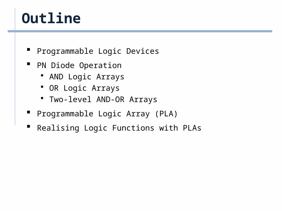
Outline
Programmable Logic Devices
PN Diode Operation AND Logic Arrays OR Logic Arrays Two-level AND-OR Arrays
Programmable Logic Array (PLA)
Realising Logic Functions with PLAs
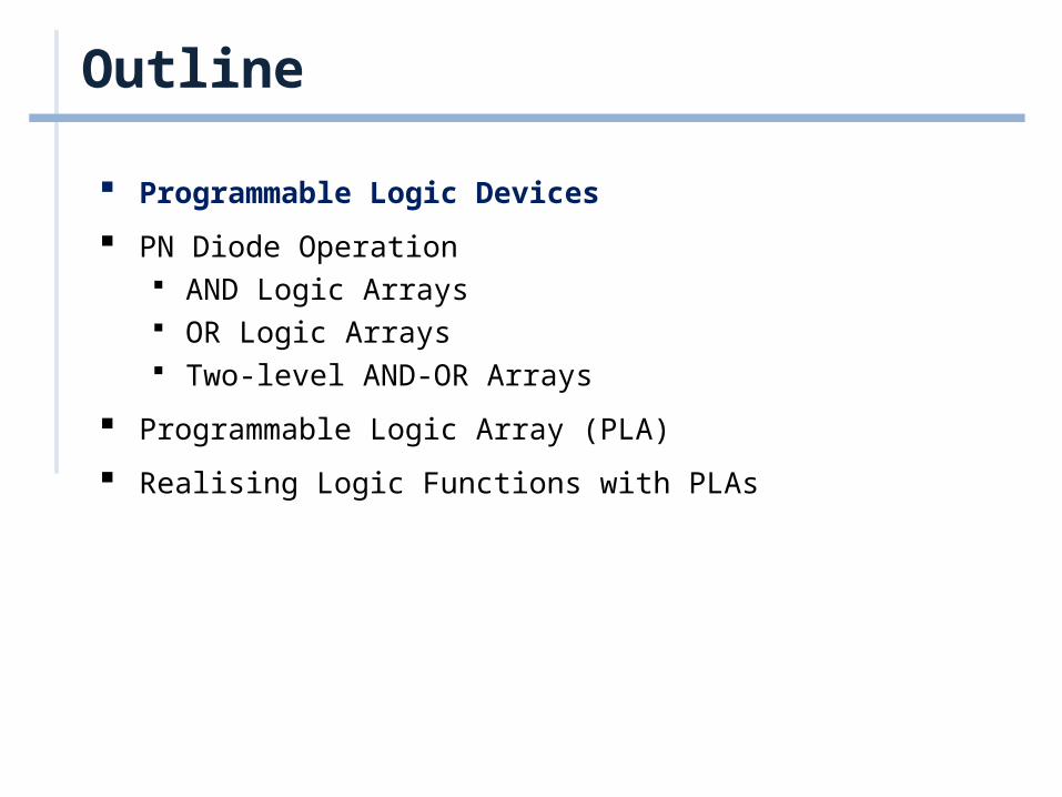
Outline
Programmable Logic Devices
PN Diode Operation AND Logic Arrays OR Logic Arrays Two-level AND-OR Arrays
Programmable Logic Array (PLA)
Realising Logic Functions with PLAs
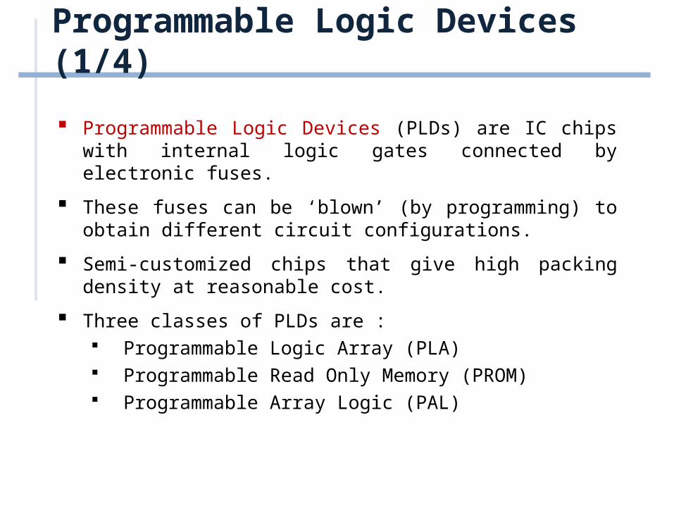
Programmable Logic Devices (1/4)
Programmable Logic Devices (PLDs) are IC chips with internal logic gates connected by electronic fuses.
These fuses can be ‘blown’ (by programming) to obtain different circuit configurations.
Semi-customized chips that give high packing density at reasonable cost.
Three classes of PLDs are : Programmable Logic Array (PLA) Programmable Read Only Memory (PROM) Programmable Array Logic (PAL)
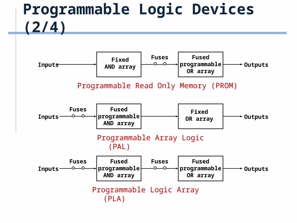
Programmable Logic Devices (2/4)
FixedAND array
Fusedprogrammable
OR array
FusesInputs Outputs
FixedOR array
Fusedprogrammable
AND array
FusesInputs Outputs
InputsFused
programmableOR array
FusesOutputs
Fuses Fusedprogrammable
AND array
Programmable Read Only Memory (PROM)
Programmable Array Logic (PAL)
Programmable Logic Array (PLA)
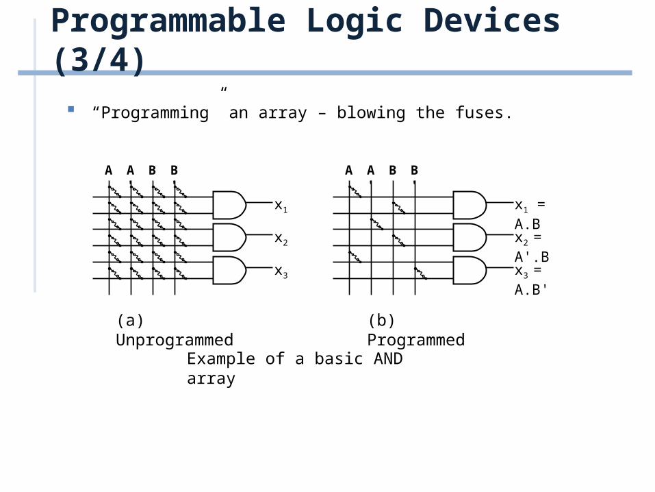
Programmable Logic Devices (3/4)
“Programming” an array – blowing the fuses.
A A' B B'
x1
x2
x3
A A' B B'
x1 = A.B
x2 = A'.B
x3 = A.B'
(a) Unprogrammed (b) Programmed
Example of a basic AND array
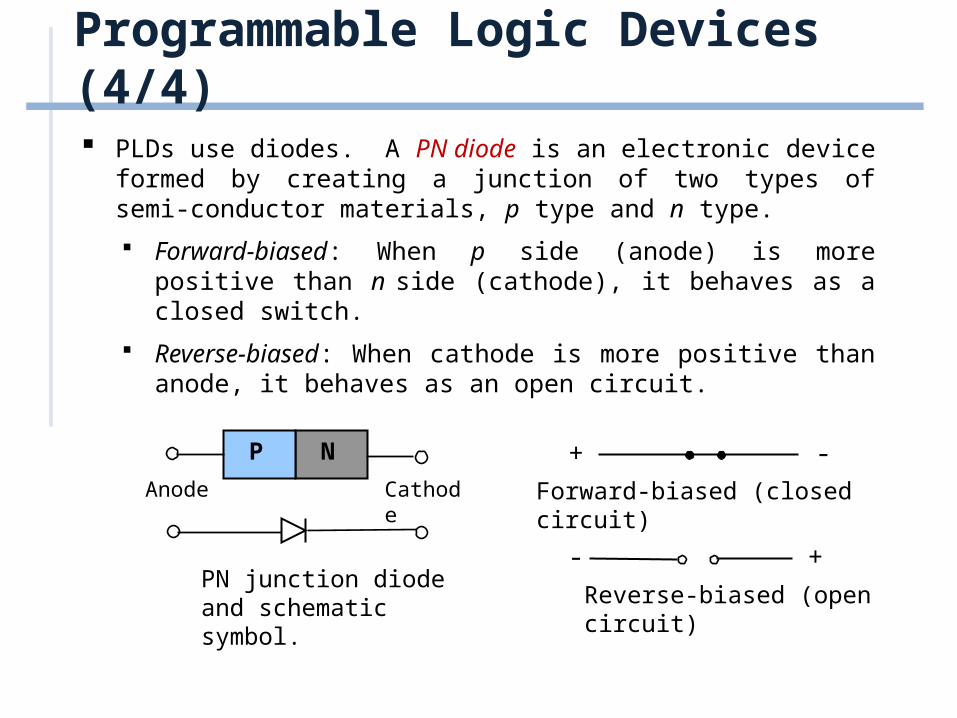
Programmable Logic Devices (4/4)
PLDs use diodes. A PN diode is an electronic device formed by creating a junction of two types of semi-conductor materials, p type and n type.
Forward-biased: When p side (anode) is more positive than n side (cathode), it behaves as a closed switch.
Reverse-biased: When cathode is more positive than anode, it behaves as an open circuit.
P N
Anode Cathode
+-
+ -
PN junction diode and schematic symbol.
Forward-biased (closed circuit)
Reverse-biased (open circuit)
Outline
Programmable Logic Devices
PN Diode Operation AND Logic Arrays OR Logic Arrays Two-level AND-OR Arrays
Programmable Logic Array (PLA)
Realising Logic Functions with PLAs
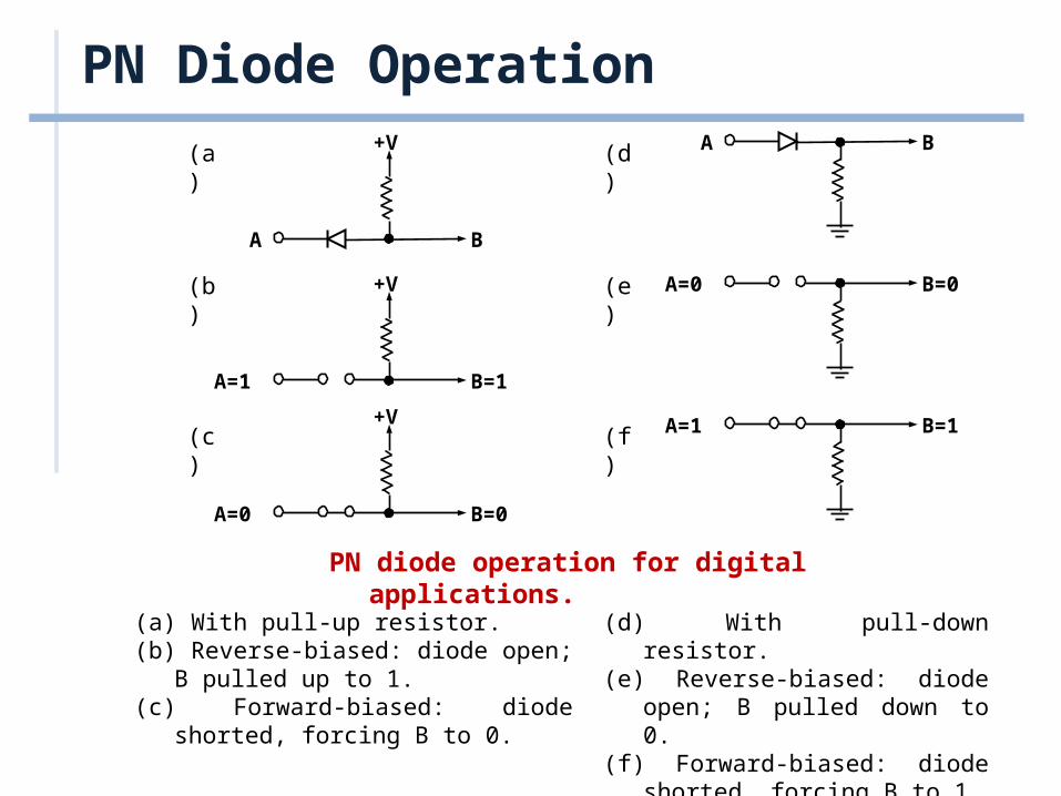
PN Diode Operation
A B
+V
A=1 B=1
+V
A=0 B=0
+V
(a)
(b)
(c)
(a) With pull-up resistor. (b) Reverse-biased: diode open; B pulled
up to 1. (c) Forward-biased: diode shorted, forcing
B to 0.
(d) With pull-down resistor. (e) Reverse-biased: diode open; B
pulled down to 0. (f) Forward-biased: diode shorted,
forcing B to 1.
PN diode operation for digital applications.
A B
A=0 B=0
A=1 B=1
(d)
(e)
(f)
Outline
Programmable Logic Devices
PN Diode Operation AND Logic Arrays OR Logic Arrays Two-level AND-OR Arrays
Programmable Logic Array (PLA)
Realising Logic Functions with PLAs
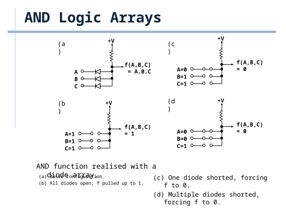
AND Logic Arrays
(a)
(b)
Af(A,B,C) = A.B.C
+V
BC
A=1f(A,B,C) = 1
+V
B=1C=1
A=0f(A,B,C) = 0
+V
B=1C=1
A=0f(A,B,C) = 0
+V
B=0C=1
(c)
(d)
(a) Basic configuration.
(b) All diodes open; f pulled up to 1.
AND function realised with a diode array.
(c) One diode shorted, forcing f to 0.
(d) Multiple diodes shorted, forcing f to 0.
Outline
Programmable Logic Devices
PN Diode Operation AND Logic Arrays OR Logic Arrays Two-level AND-OR Arrays
Programmable Logic Array (PLA)
Realising Logic Functions with PLAs
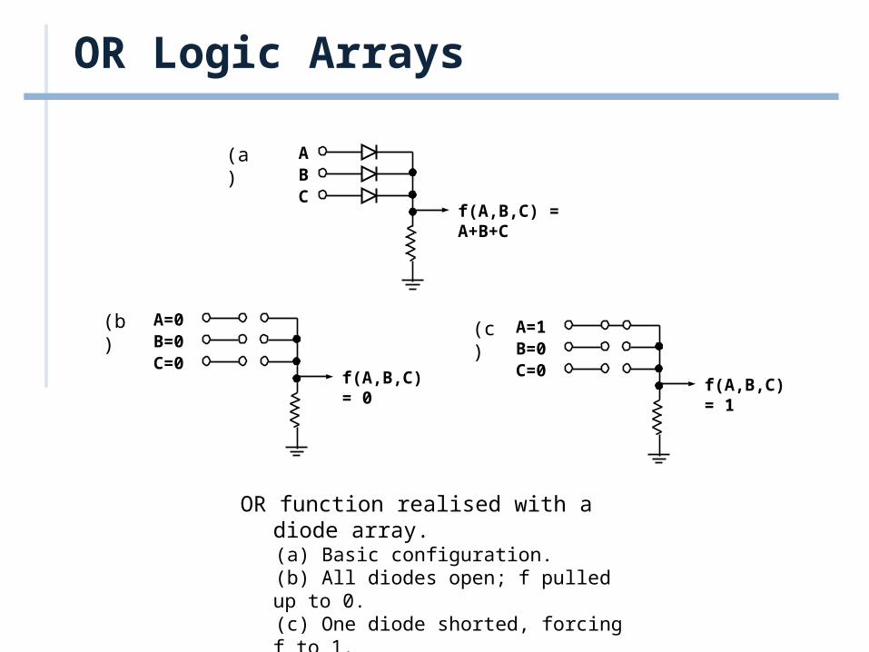
OR Logic Arrays
A
f(A,B,C) = A+B+C
BC
A=0
f(A,B,C) = 0
B=0C=0
A=1
f(A,B,C) = 1
B=0C=0
(a)
(b) (c)
OR function realised with a diode array. (a) Basic configuration. (b) All diodes open; f pulled up to 0. (c) One diode shorted, forcing f to 1.
Outline
Programmable Logic Devices
PN Diode Operation AND Logic Arrays OR Logic Arrays Two-level AND-OR Arrays
Programmable Logic Array (PLA)
Realising Logic Functions with PLAs
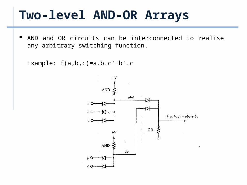
Two-level AND-OR Arrays
AND and OR circuits can be interconnected to realise any arbitrary switching function.
Example: f(a,b,c)=a.b.c'+b'.c
Outline
Programmable Logic Devices
PN Diode Operation AND Logic Arrays OR Logic Arrays Two-level AND-OR Arrays
Programmable Logic Array (PLA)
Realising Logic Functions with PLAs
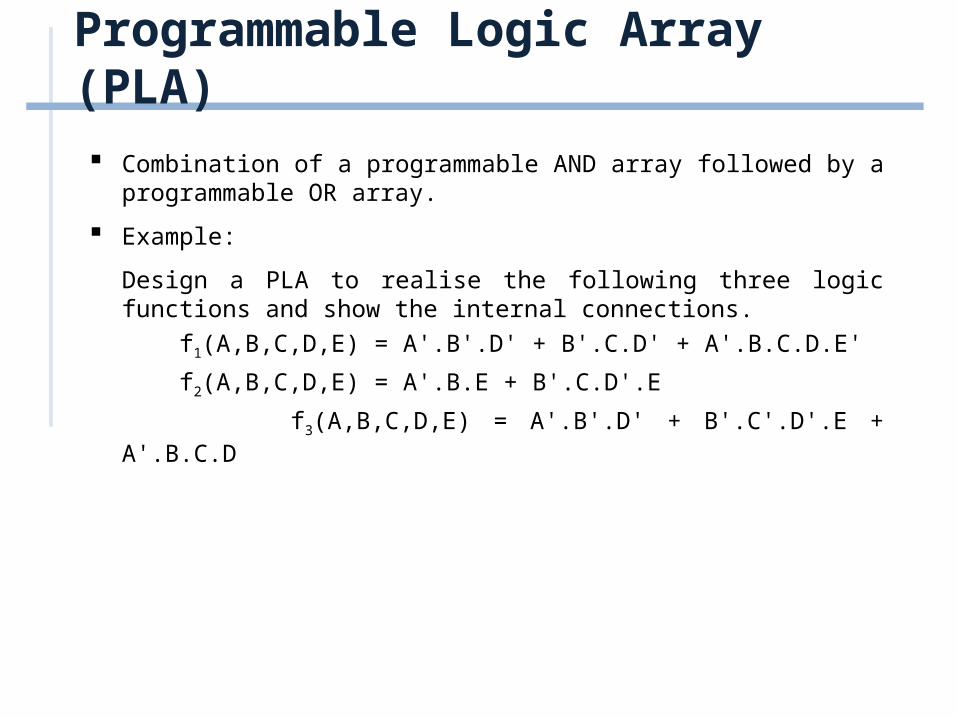
Programmable Logic Array (PLA)
Combination of a programmable AND array followed by a programmable OR array.
Example:
Design a PLA to realise the following three logic functions and show the internal connections.
f1(A,B,C,D,E) = A'.B'.D' + B'.C.D' + A'.B.C.D.E'
f2(A,B,C,D,E) = A'.B.E + B'.C.D'.E
f3(A,B,C,D,E) = A'.B'.D' + B'.C'.D'.E + A'.B.C.D
Outline
Programmable Logic Devices
PN Diode Operation AND Logic Arrays OR Logic Arrays Two-level AND-OR Arrays
Programmable Logic Array (PLA)
Realising Logic Functions with PLAs
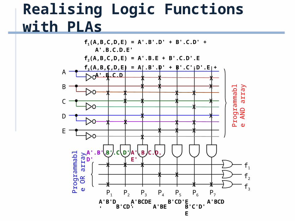
Realising Logic Functions with PLAsf1(A,B,C,D,E) = A'.B'.D' + B'.C.D' + A'.B.C.D.E'
f2(A,B,C,D,E) = A'.B.E + B'.C.D'.E
f3(A,B,C,D,E) = A'.B'.D' + B'.C'.D'.E + A'.B.C.D
A
B
C
D
E
P1 P3 P4 P6P5P2 P7
Pro
gram
mab
le
OR
arr
ay
Pro
gram
mab
le
AN
D a
rray
A'B'D'
X
X
X
B'CD'
X
X
X
X
X
X
X
X
A'BCDE'A'BE
X
X
X
X
X
X
X
B'CD'EB'C'D'E
X
X
X
X
A'BCD
X
X
X
X
f1
f2
f3
X X X
X X
X X X
A'.B'.D' B'.C.D' A'.B.C.D.E'