Embed Size (px)
Citation preview
Df dfs
UNDERSTANDING
PROGRAMMABLE LOGIC
Understanding GAL devices within the context of the
various N8VEM projects.
THE GAL 22V10

June 21th, 2014 – Document Version 1.6
The PAL and GAL – An introduction
This paper contains original material plus content I copied from information found on the internet. I’ve edited
some of the found content to remove unnecessary references; to reformat it and to clean it up a bit. Where
possible I’ve tried to give credit to the original authors or sources.
I’m very new to the world of programmable logic; I can’t guarantee the accuracy of the content although I’ve tried
to make it as accurate as possible.
The intent of the document is to help those who are new to programmable logic come up to speed in the context
of the N8VEM efforts. As the N8VEM boards become more complex we will need to start using programmable
logic to help the designs fit on a single board.
Most likely one or more of the members of the N8VEM work will be able to provide programmed GAL devices to
those who don’t have a GAL programmer. I’ve recently purchased a GAL programmer and will be able to help
provide programmed GALs.
The portions I wrote fall under the Creative Commons NC (Non‐Commercial) license. You may reuse it or modify it
as long as the resulting material continues to be free and you list the original source and author. Commercial use is
restricted. I want the material to be useful; reuse is encouraged. If you reuse it please let me know.
Please feel free to send feedback, corrections etc. to me at [email protected]
Thanks.
Neil B. Breeden II

TABLE OF CONTENTS
introduction ................................................................................................................................................................... 2
The 22V10 – A great place to start ................................................................................................................................ 3
PALs, GALs, PALASM and the Device Programmer ........................................................................................................ 4
PALASM Supported Devices .......................................................................................................................................... 5
Defining the logic for the GAL ........................................................................................................................................ 6
Reading the equations ................................................................................................................................................... 9
Let’s look an example PDS file. .................................................................................................................................... 10
Some Best Practices, Notes, Ramblings and Comments…. .......................................................................................... 13
My Testing Rig for 22V10 GALs .................................................................................................................................... 14
Typical 22V10s and the generic GAL 22V10 pinout: .................................................................................................... 15
Resources .................................................................................................................................................................... 16
The Design Cycle .......................................................................................................................................................... 17
Programmable logic devices ........................................................................................................................................ 18
Boolean functions ........................................................................................................................................................ 19
PALASM Language Guide ............................................................................................................................................. 22
Design with Boolean Equations ............................................................................................................................... 22
Design with State Machines .................................................................................................................................... 23
Simulation ............................................................................................................................................................... 25
Simulation Commands ........................................................................................................................................ 25
Writing Simulations............................................................................................................................................. 30
Interpreting Simulation Results .......................................................................................................................... 30
.PDS file Vocabulary ..................................................................................................................................................... 31
Characters ............................................................................................................................................................... 31
Legal .................................................................................................................................................................... 31
Illegal ................................................................................................................................................................... 31
Lines ........................................................................................................................................................................ 31
Reserved Words ...................................................................................................................................................... 31
Special Symbols ....................................................................................................................................................... 32
Operator Precedence .............................................................................................................................................. 33
State Machine Symbols ........................................................................................................................................... 33
Boolean Design Grammar ............................................................................................................................................ 34
State Machine Design Grammar .................................................................................................................................. 35
1
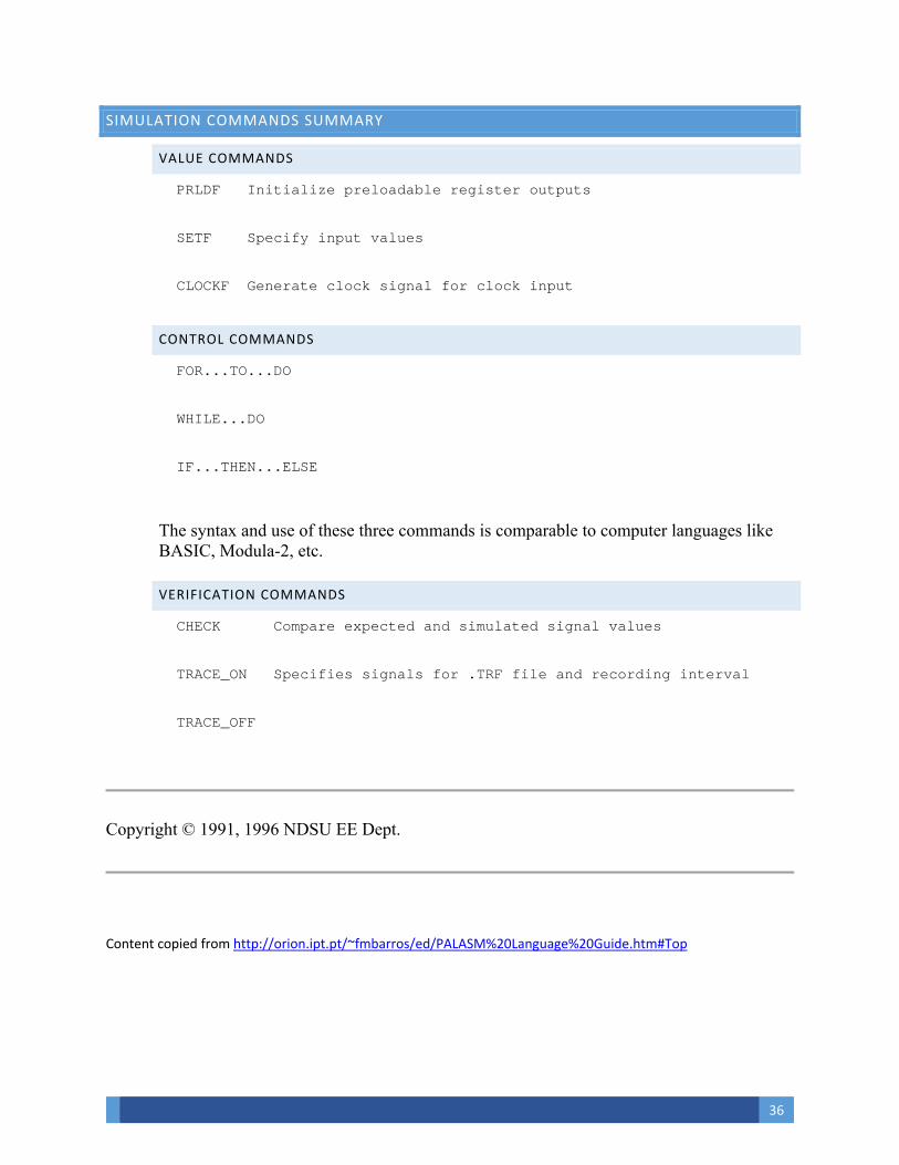
Simulation Commands Summary ................................................................................................................................ 36
Value Commands .................................................................................................................................................... 36
Control Commands.................................................................................................................................................. 36
Verification Commands ........................................................................................................................................... 36
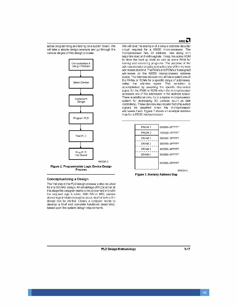
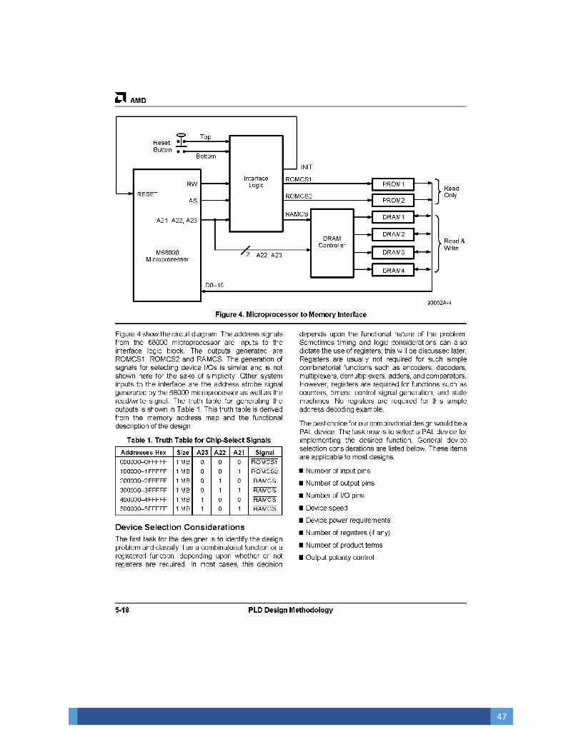
PLD Design Methodology ............................................................................................................................................ 45
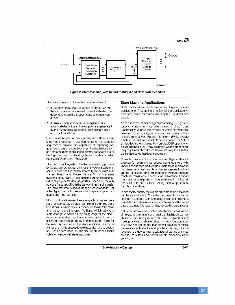
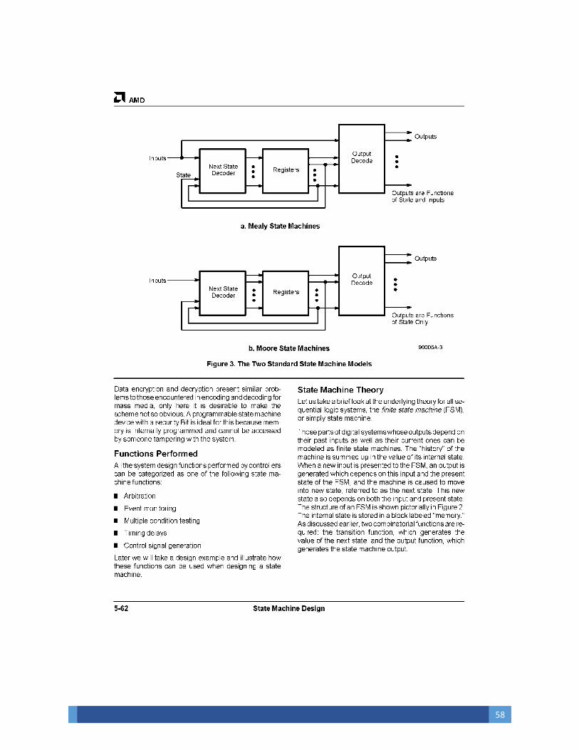
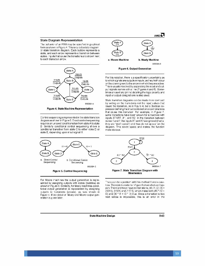
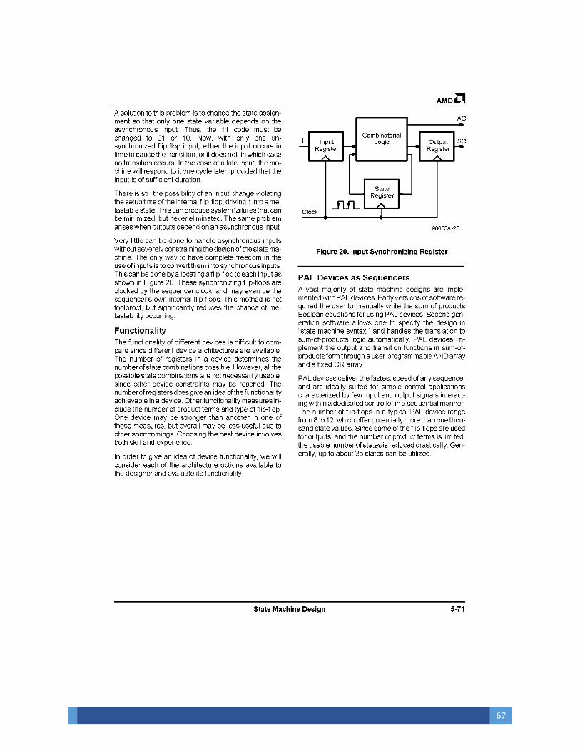
STATE MACHINE DESIGN ............................................................................................................................................. 56
Registered logic Design ................................................................................................................................................ 69
Example Execution of PALASM .................................................................................................................................... 89

2
INTRODUCTION
Traditional logic such as the TTL ICs used in most of the N8VEM designs are dedicated to the function they provide.
The 74LS00 has four 2‐input AND Gates; the 74LS04 has six inverters (NOT gates).
Some N8VEM boards already use programmable devices such as EPROMs and FLASH memories. Typically these
contain software (firmware) that the microprocessor requires for the system to operate. EPROM and FLASH can
also be used to store look up tables; character sets for video boards and many other things.
The use of GALs will expand the range of boards that can be designed as part of the N8VEM project.
Programmable logic allows you to customize the IC to provide the exact function you need. They can have tens or
hundreds of logic gates in a single IC. By programming the device you customize which gates and combinations of
gates are to be used. It might take 5 regular TTL ICs to create an address decoder; the same functionality can be
defined in a single programmable device. Instead of 5 ICs on the printed circuit board we only need one; this frees
up space one the board for other functionality.
3
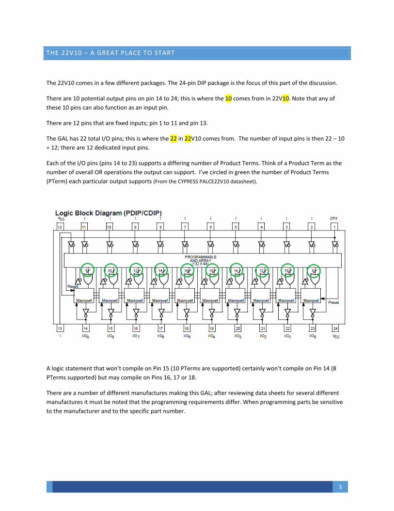
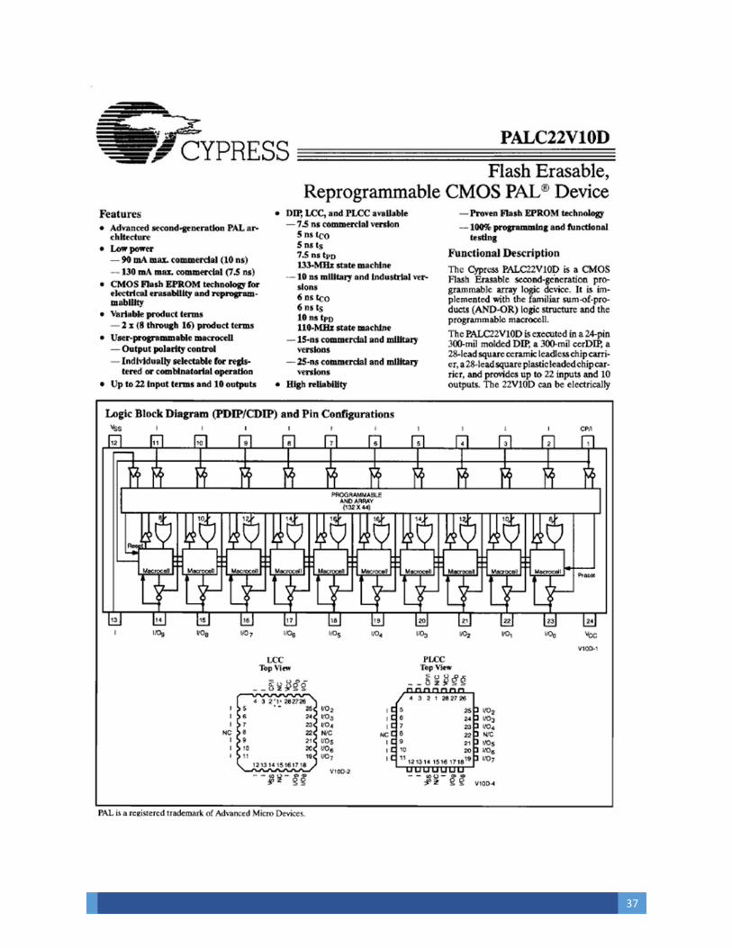
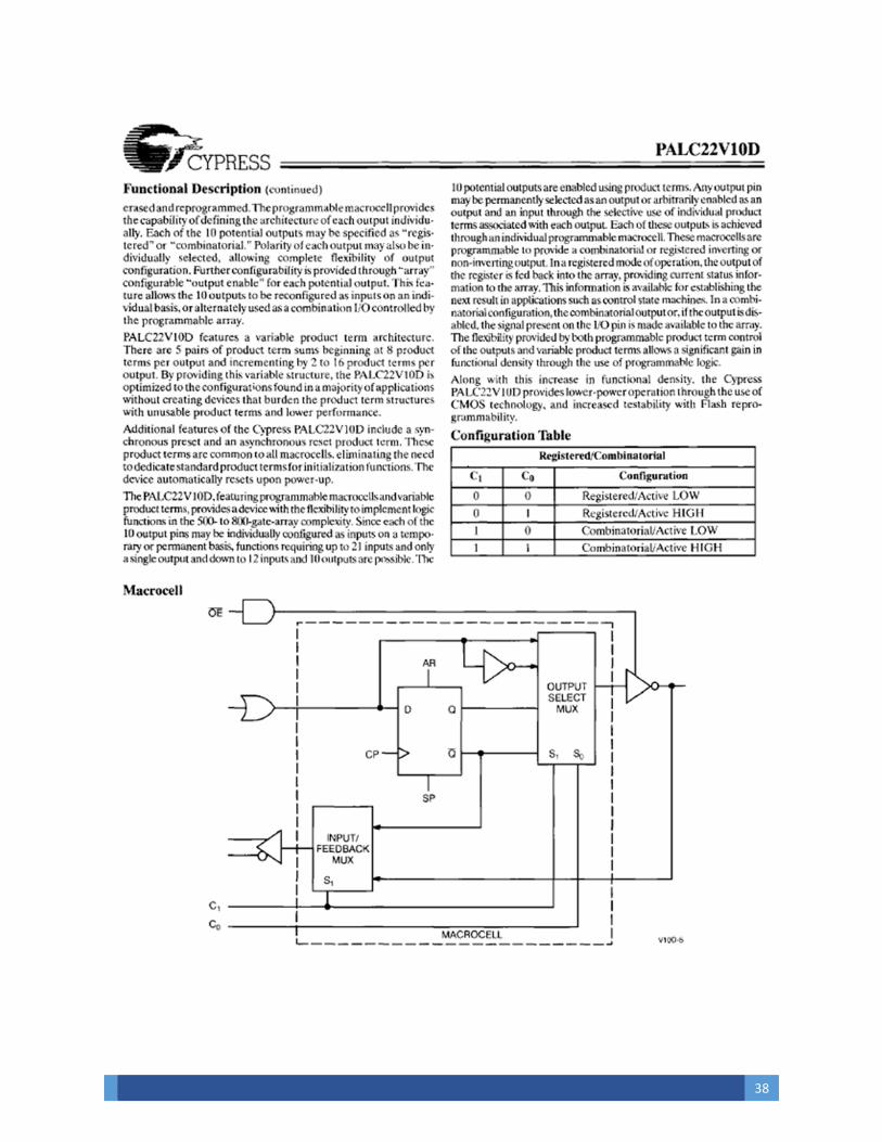
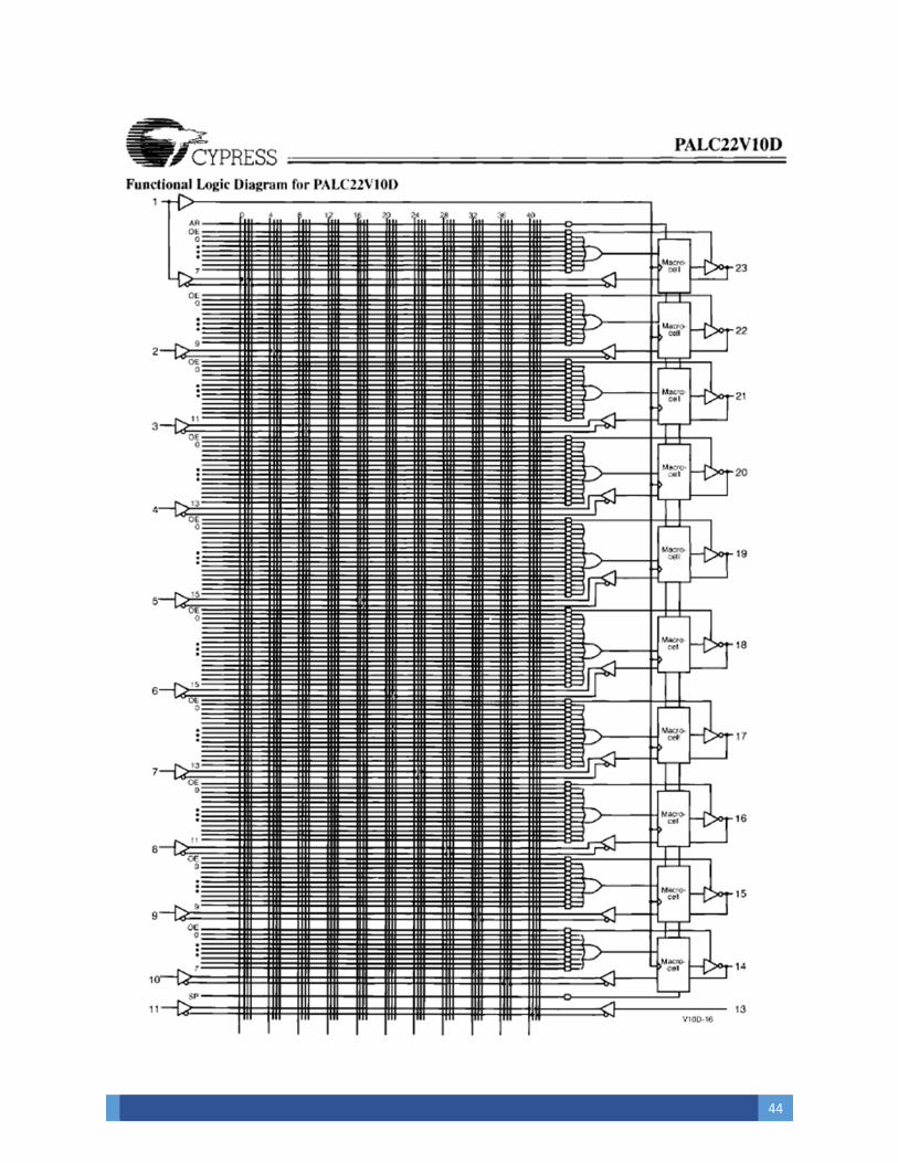
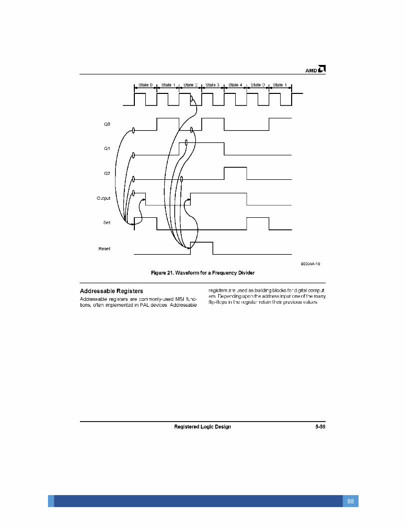
THE 22V10 – A GREAT PLACE TO START
The 22V10 comes in a few different packages. The 24‐pin DIP package is the focus of this part of the discussion.
There are 10 potential output pins on pin 14 to 24; this is where the 10 comes from in 22V10. Note that any of
these 10 pins can also function as an input pin.
There are 12 pins that are fixed inputs; pin 1 to 11 and pin 13.
The GAL has 22 total I/O pins; this is where the 22 in 22V10 comes from. The number of input pins is then 22 – 10
= 12; there are 12 dedicated input pins.
Each of the I/O pins (pins 14 to 23) supports a differing number of Product Terms. Think of a Product Term as the
number of overall OR operations the output can support. I’ve circled in green the number of Product Terms
(PTerm) each particular output supports (From the CYPRESS PALCE22V10 datasheet).
A logic statement that won’t compile on Pin 15 (10 PTerms are supported) certainly won’t compile on Pin 14 (8
PTerms supported) but may compile on Pins 16, 17 or 18.
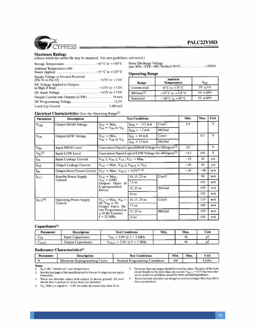
There are a number of different manufactures making this GAL; after reviewing data sheets for several different
manufactures it must be noted that the programming requirements differ. When programming parts be sensitive
to the manufacturer and to the specific part number.

4
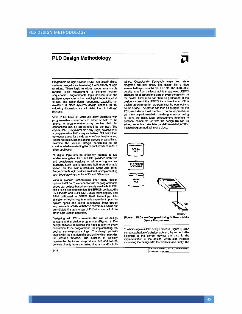
PALS, GALS, PALASM AND THE DEVICE PROGRAMMER
PALs are one time programmable devices; GALs can be erased and reprogrammed a limited number of
times.
The GAL version of a device is functionally equivalent to the PAL version.
PALASM is a program that inputs the definition of the function to be implemented and outputs a file that
the device programmer can use to ‘program the device’.
PALASM compiles .PDS files; it outputs a .JED file.
The .JED file is the programming definition for a generic type of device. Example: You use PALASM to
compile for a ‘PAL22V10’ device, a .JED file is created. You can then program a ‘GAL22V10’ device using
the .JED file from PALASM. The .JED file is the generic programming map for a ‘22V10’ – it doesn’t care if
the device is a PAL22V10 or a GAL22V10.
My programmer is a Wellon VP‐390; it allows me to test the GAL after programming it at +/‐ 10 percent of
VCC. I highly recommend enabling these tests as part of your programming cycle.
The Wellon VP‐290 also appears to be a good choice for a general purpose programmer.
If you make the decision to buy a programmer consider buying a higher quality unit. There are many
cheap programmers on eBay; my experience with these has been pretty poor. I would strongly suggest
consulting the N8VEM forums for advice before you commit to a programmer.
5
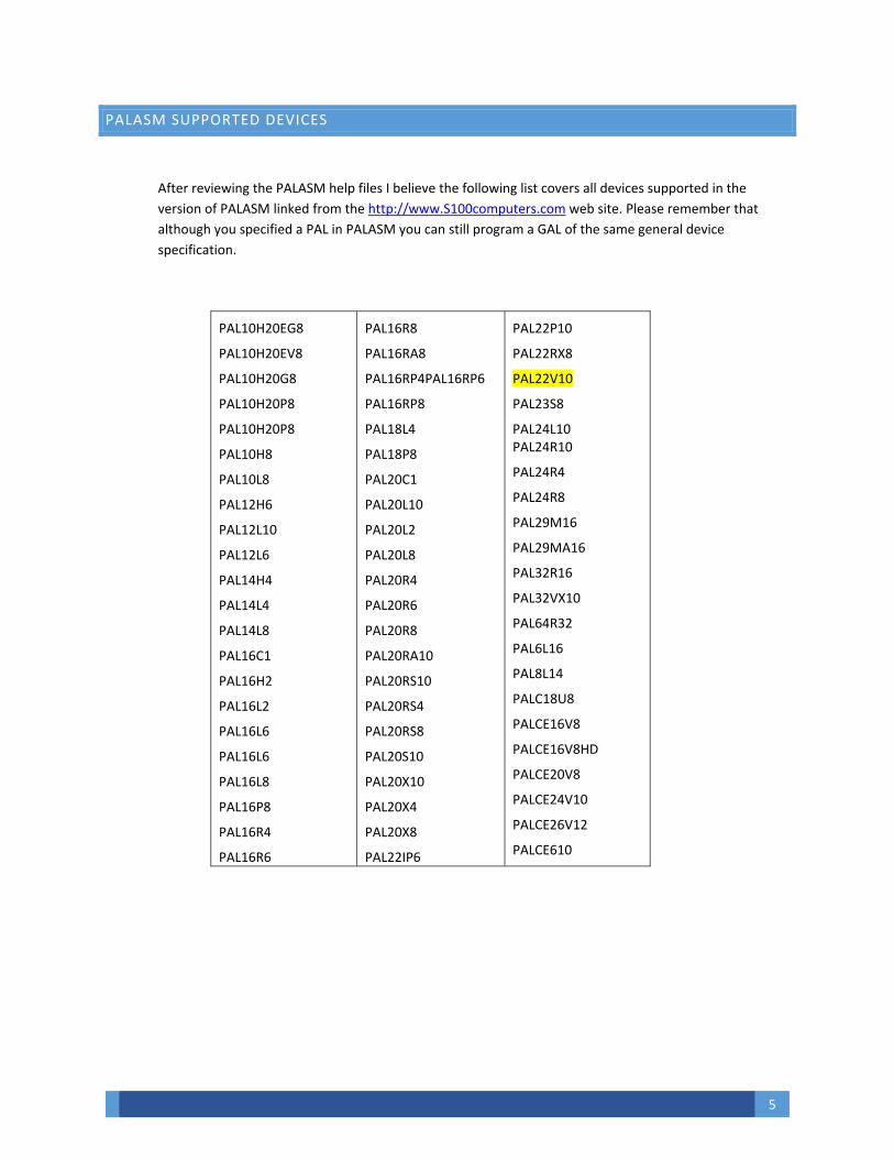
PALASM SUPPORTED DEVICES
After reviewing the PALASM help files I believe the following list covers all devices supported in the
version of PALASM linked from the http://www.S100computers.com web site. Please remember that
although you specified a PAL in PALASM you can still program a GAL of the same general device
specification.
PAL10H20EG8
PAL10H20EV8
PAL10H20G8
PAL10H20P8
PAL10H20P8
PAL10H8
PAL10L8
PAL12H6
PAL12L10
PAL12L6
PAL14H4
PAL14L4
PAL14L8
PAL16C1
PAL16H2
PAL16L2
PAL16L6
PAL16L6
PAL16L8
PAL16P8
PAL16R4
PAL16R6
PAL16R8
PAL16RA8
PAL16RP4PAL16RP6
PAL16RP8
PAL18L4
PAL18P8
PAL20C1
PAL20L10
PAL20L2
PAL20L8
PAL20R4
PAL20R6
PAL20R8
PAL20RA10
PAL20RS10
PAL20RS4
PAL20RS8
PAL20S10
PAL20X10
PAL20X4
PAL20X8
PAL22IP6
PAL22P10
PAL22RX8
PAL22V10
PAL23S8
PAL24L10 PAL24R10
PAL24R4
PAL24R8
PAL29M16
PAL29MA16
PAL32R16
PAL32VX10
PAL64R32
PAL6L16
PAL8L14
PALC18U8
PALCE16V8
PALCE16V8HD
PALCE20V8
PALCE24V10
PALCE26V12
PALCE610
6
DEFINING THE LOGIC FOR THE GAL
Being comfortable with the following will go a long way towards helping you define the required logic for your
design.
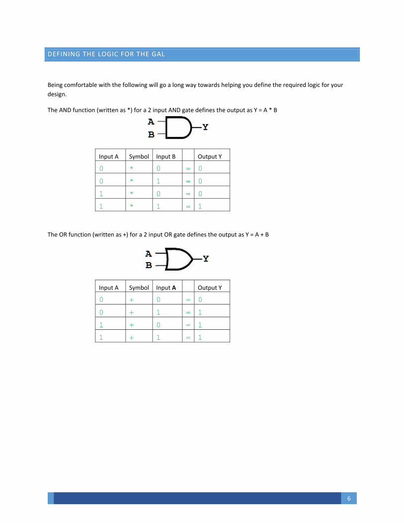
The AND function (written as *) for a 2 input AND gate defines the output as Y = A * B
Input A Symbol Input B Output Y
0 * 0 = 0
0 * 1 = 0
1 * 0 = 0
1 * 1 = 1
The OR function (written as +) for a 2 input OR gate defines the output as Y = A + B
Input A Symbol Input A Output Y
0 + 0 = 0
0 + 1 = 1
1 + 0 = 1
1 + 1 = 1
7
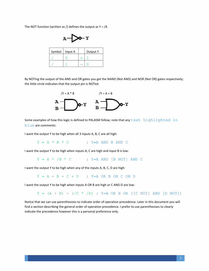
The NOT function (written as /) defines the output as Y = /A
Symbol Input A Output Y
/ 0 = 1
/ 1 = 0
By NOTing the output of the AND and OR gates you get the NAND (Not AND) and NOR (Not OR) gates respectively;
the little circle indicates that the output pin is NOTed.
/Y = A * B /Y = A + B
Some examples of how this logic is defined to PALASM follow; note that any text highlighted in blue are comments:
I want the output Y to be high when all 3 inputs A, B, C are all high:
Y = A * B * C ; Y=A AND B AND C
I want the output Y to be high when inputs A, C are high and input B is low:
Y = A * /B * C ; Y=A AND [B NOT] AND C
I want the output Y to be high when any of the inputs A, B, C, D are high:
Y = A + B + C + D ; Y=A OR B OR C OR D
I want the output Y to be high when inputs A OR B are high or C AND D are low:
Y = (A + B) + (/C * /D) ; Y=A OR B OR ([C NOT] AND [D NOT])
Notice that we can use parenthesizes to indicate order of operation precedence. Later in this document you will
find a section describing the general order of operation precedence. I prefer to use parenthesizes to clearly
indicate the precedence however this is a personal preference only.
8
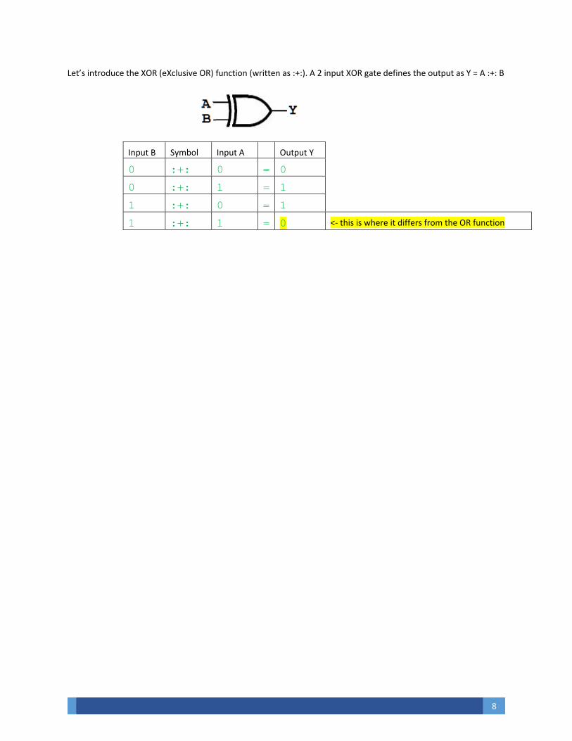
Let’s introduce the XOR (eXclusive OR) function (written as :+:). A 2 input XOR gate defines the output as Y = A :+: B
Input B Symbol Input A Output Y
0 :+: 0 = 0
0 :+: 1 = 1
1 :+: 0 = 1
1 :+: 1 = 0 <‐ this is where it differs from the OR function
9
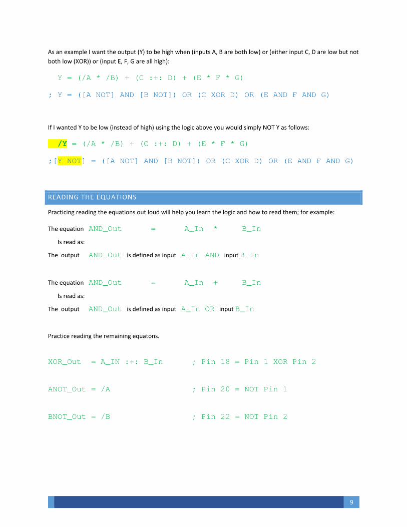
As an example I want the output (Y) to be high when (inputs A, B are both low) or (either input C, D are low but not
both low (XOR)) or (input E, F, G are all high):
Y = (/A * /B) + (C :+: D) + (E * F * G)
; Y = ([A NOT] AND [B NOT]) OR (C XOR D) OR (E AND F AND G)
If I wanted Y to be low (instead of high) using the logic above you would simply NOT Y as follows:
/Y = (/A * /B) + (C :+: D) + (E * F * G)
;[Y NOT] = ([A NOT] AND [B NOT]) OR (C XOR D) OR (E AND F AND G)
READING THE EQUATIONS
Practicing reading the equations out loud will help you learn the logic and how to read them; for example:
The equation AND_Out = A_In * B_In
Is read as:
The output AND_Out is defined as input A_In AND input B_In
The equation AND_Out = A_In + B_In
Is read as:
The output AND_Out is defined as input A_In OR input B_In
Practice reading the remaining equatons.
XOR_Out = A_IN :+: B_In ; Pin 18 = Pin 1 XOR Pin 2
ANOT_Out = /A ; Pin 20 = NOT Pin 1
BNOT_Out = /B ; Pin 22 = NOT Pin 2
10
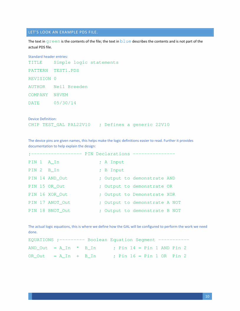
LET’S LOOK AN EXAMPLE PDS FILE.
The text in green is the contents of the file; the text in blue describes the contents and is not part of the actual PDS file.
Standard header entries: TITLE Simple logic statements
PATTERN TEST1.PDS
REVISION 0
AUTHOR Neil Breeden
COMPANY N8VEM
DATE 05/30/14
Device Definition: CHIP TEST_GAL PAL22V10 ; Defines a generic 22V10
The device pins are given names, this helps make the logic definitions easier to read. Further it provides
documentation to help explain the design:
;------------------ PIN Declarations ---------------
PIN 1 A_In ; A Input
PIN 2 B_In ; B Input
PIN 14 AND_Out ; Output to demonstrate AND
PIN 15 OR_Out ; Output to demonstrate OR
PIN 16 XOR_Out ; Output to Demonstrate XOR
PIN 17 ANOT_Out ; Output to demonstrate A NOT
PIN 18 BNOT_Out ; Output to demonstrate B NOT
The actual logic equations, this is where we define how the GAL will be configured to perform the work we need
done.
EQUATIONS ;--------- Boolean Equation Segment -----------
AND_Out = A_In * B_In ; Pin 14 = Pin 1 AND Pin 2
OR_Out = A_In + B_In ; Pin 16 = Pin 1 OR Pin 2
11
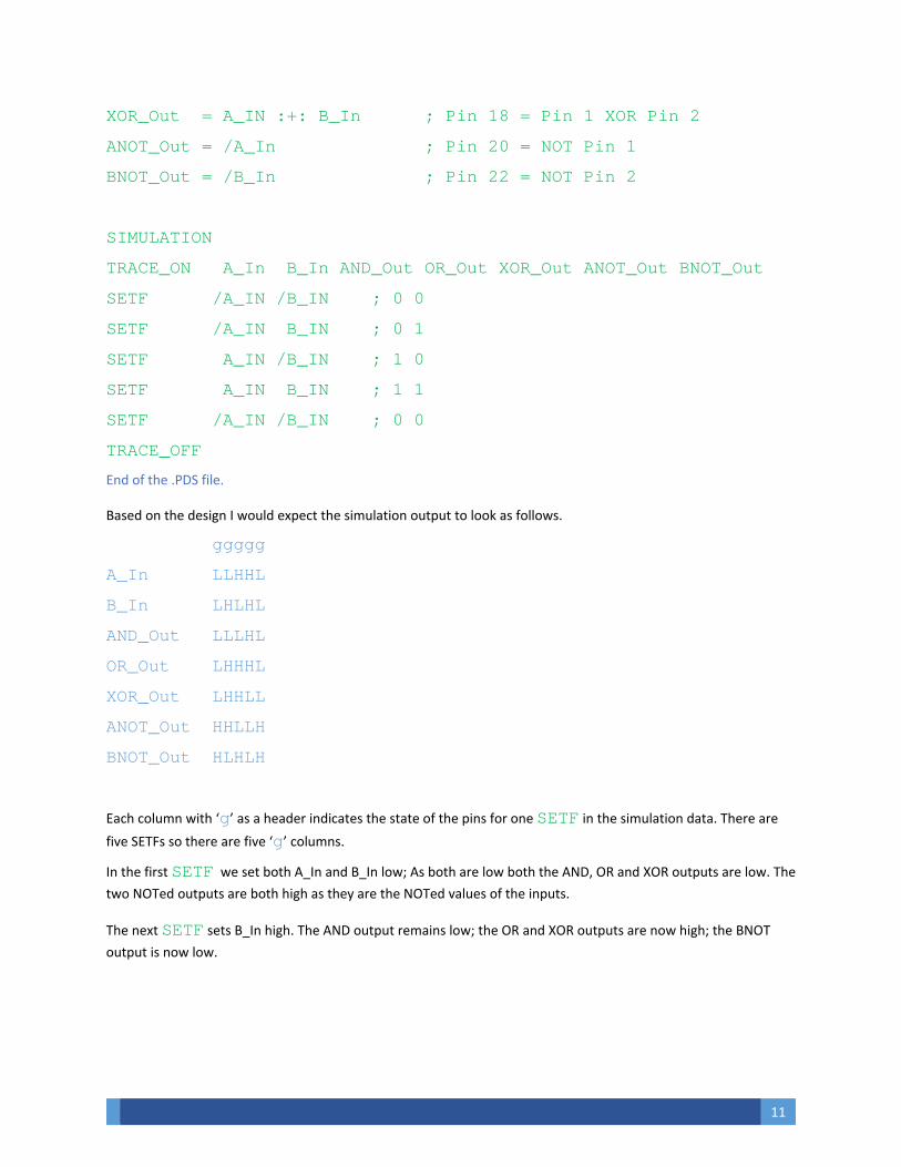
XOR_Out = A_IN :+: B_In ; Pin 18 = Pin 1 XOR Pin 2
ANOT_Out = /A_In ; Pin 20 = NOT Pin 1
BNOT_Out = /B_In ; Pin 22 = NOT Pin 2
SIMULATION
TRACE_ON A_In B_In AND_Out OR_Out XOR_Out ANOT_Out BNOT_Out
SETF /A_IN /B_IN ; 0 0
SETF /A_IN B_IN ; 0 1
SETF A_IN /B_IN ; 1 0
SETF A_IN B_IN ; 1 1
SETF /A_IN /B_IN ; 0 0
TRACE_OFF
End of the .PDS file.
Based on the design I would expect the simulation output to look as follows.
ggggg
A_In LLHHL
B_In LHLHL
AND_Out LLLHL
OR_Out LHHHL
XOR_Out LHHLL
ANOT_Out HHLLH
BNOT_Out HLHLH
Each column with ‘g’ as a header indicates the state of the pins for one SETF in the simulation data. There are
five SETFs so there are five ‘g’ columns.
In the first SETF we set both A_In and B_In low; As both are low both the AND, OR and XOR outputs are low. The two NOTed outputs are both high as they are the NOTed values of the inputs.
The next SETF sets B_In high. The AND output remains low; the OR and XOR outputs are now high; the BNOT
output is now low.

12
Can you explain the remaining columns results?
On pin 19 add a NOR PTerm along with the simulation data.
Add a more complex PTerm such as Y = ((A * B) + (C * D) * E)
What would the simulation data look like?
What would the simulation output look like?
13
SOME BEST PRACTICES, NOTES, RAMBLINGS AND COMMENTS….
Different manufactures of the same device type can have very different programming requirements. I damaged 4
Lattice parts when I programmed them using the definition for a NS device. The Lattice part wanted 9 volts for
VPP; the NS part wanted 14 volts for VPP. This is also true for EPROMS, FLASH etc. An Intel 2764 has a different
programming configuration then an Intel 27C64. VPP refers to the programming voltage applied to the device to
erase or program it.
An erased GAL has all PTerms functionality enabled; this will result in all of the output pins always being high; keep
this in mind.
When erased the output is basically defined as “Output = (A * B) + (/A * B) + (A * /B) etc….”, this results in the
output always being true (high). By programming you disable the unneeded terms.
I was confused several times thinking my design wasn’t working when in reality the GAL was erased due to the fact
that the software my VP‐390 uses clears the data buffer each time the GAL type is changed; this includes changing
the manufacture for the same type of GAL. With the buffer cleared a programming pass will leave the device
erased. You may need to reload the .JED file after changing devices.
Using LEDs, a breadboard and jumper wires you can build a test rig to allow you to do a basic verify test to see if
the programmed device works as expected. This is HIGHLY recommended as trying to debug a design in circuit is
very difficult.
Don’t be afraid to fail; you may destroy a few parts; your designs may not work initially or they may not represent
what you were trying to do. This is OK, you should stay with it and try to understand why it failed; this is where the
BEST learning comes from.
Reach out and ask for help when needed. This is why we have the N8VEM forums. For me there are times when
the act of typing the question; of trying to explain the problem will suddenly give me insight that allows me to fix it
or to try something different.
Keep notes; keep notes; be sure to keep notes. I keep detailed notes as I work on a design; when I solder up a
board; when I write code etc. I go so far as to scan 200dpi and 600dpi images of both side of the blank PCB before I
begin to assemble it. Again, get in the practice of keeping notes.
Review the forums first. I’m guilty of not always doing this; it is however a practice I’m working on getting into.
Share your experiences, share your successes, and share your failures. As a community we learn together.
14
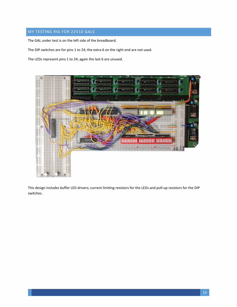
MY TESTING RIG FOR 22V10 GALS
The GAL under test is on the left side of the breadboard.
The DIP switches are for pins 1 to 24; the extra 6 on the right end are not used.
The LEDs represent pins 1 to 24; again the last 6 are unused.
This design includes buffer LED drivers; current limiting resistors for the LEDs and pull‐up resistors for the DIP
switches.
15
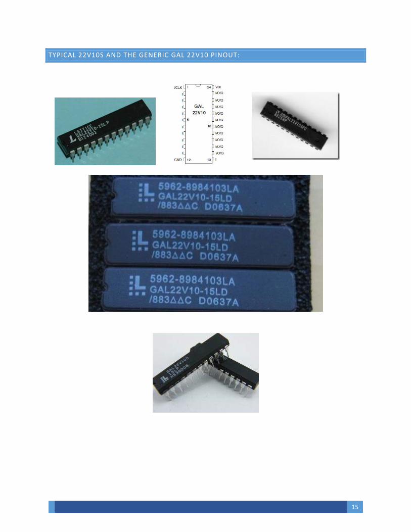
TYPICAL 22V10S AND THE GENERIC GAL 22V10 PINOUT:

16
RESOURCES
S100 Computers discussion of GALs
Includes instructions on downloading PALASM and getting it to run:
http://www.s100computers.com/My%20System%20Pages/ISA%20to%20S100%20Bus/Intro%20To%20GA
Ls.htm
Examples of various logic implementations:
http://orion.ipt.pt/~fmbarros/ed/palasmex.pdf
A lot of good reviews and insights into good tools along with a lot of good material on electronics:
www.eevblog.com
Videos lectures on electronics and GALs:
http://www.allaboutcircuits.com/videos/index.html
http://www.allaboutcircuits.com/videos/89.html
Interesting information ‐ the preview doesn’t show all pages but there is a lot of interesting material presented:
An interesting book on Google Books
Other links:
http://mazsola.iit.uni‐miskolc.hu/cae/docs/theor00.html
http://ee.sharif.edu/~logic_circuits_t/readings/PLD.pdf
http://sourceforge.net/projects/logiccircuitd/?source=directory
17
THE DESIGN CYCLE
Plan, Document, Execute, Document, Test, Document – repeat as required.
1. Define the requirements – what is the problem to be solved?
a. Document it – if you can’t clearly and completely describe it then you are not ready to move to
the next step.
2. Decide how you want to solve it; in this example I am assuming you will be using a PLD.
a. Document the pro’s and con’s to the various approaches you consider.
3. Define the inputs and outputs for the projects.
a. Document it – if you can’t clearly and completely describe them then you are not ready to move
to the next step.
4. You should be able to define a simulation data set for PALASM; if you can’t then you most likely don’t
understand your design sufficiently to test the programmed part.
a. Document it.
5. Create or update the PALASM PDS file.
6. Using PALASM compile the PSD file; fix any bugs and compile again until you get a clean compile.
7. Simulate the design in PASASM; repeat steps 5 thru 7 until the simulation is successful.
8. Program a GAL using the JED file produced by PALASM.
a. Be sure to select the correct manufacture and device in the programming software.
b. Be sure to load / reload the .JED file as required; changing the device or manufacturer of a device
will require you to reload the JED file.
9. Test the design on a breadboard; repeat steps 5 thru 9 until it works on the breadboard.
10. Make a backup copy the PDS file. Rename it to include the time and date.
a. You may end up with multiple copies; I believe it’s safest to keep them all as you can revert back
to an older one if needed.
11. Test in the application, repeat steps 5 thru 11 until it works in the application.

18
All content below this point was copied from resources found on the internet.
PROGRAMMABLE LOGIC DEVICES
Programmable Logic Devices (PLDs) (also known as PALs) are popular devices for implementing digital designs. These devices can be used where earlier systems used TTL or CMOS logic ICs. The PLDASM is a tool that allows Boolean equations to be programmed into a PLD in order to perform a user‐defined logic function. Boolean equations make it possible to describe a function in an efficient manner, and this assures that the designer achieves the most compact solution with the fastest propagation delays. Furthermore, with Boolean equations the PLD can function as an address decoder, state machine or counter, and perform any number of other tasks ranging from the simple to the complex. While initially PLDs provided a savings in the amount of space used on a PC board, recent high speed PLDs are often significantly faster than the equivalent circuit implemented in TTL logic. Another recent development in PLDs is the complexity of the macrocells used for I/O. PLDASM automatically configures these macrocells, according to a set of simple rules which apply to all the PLDs supported by PLDASM. This allows substitution of one device for another, and reduces the amount of time required to 'learn' a new PLD.
A PLDs internal structure is built as an AND/OR matrix. A programmable input AND array can generate any AND function of all device inputs (with or without inversion). These AND functions are called 'Product Terms'. Product terms feed a multiple input OR gate. Since the AND/OR matrix can express any Boolean transfer function, the flexibility and functionality of a PLD is limited only by the number of terms available in the AND ‐ OR arrays. PLD devices are available in different sizes, some with over 40 inputs, and some with up to 19 Product Terms per output. The outputs range from simple tri‐state drivers to complex registered macrocells with programmable inverters.
19
BOOLEAN FUNCTIONS
In an un‐programmed PLD, all fuses are intact. In other words, every input line is 'ANDed' with all other input lines (including any feedback terms available in the device) The output of these AND functions is fed into an OR gate and is then either fed onto more complex functions or presented directly on the output pins of the device.
For example, let us assume that we have a simple PLD with two input terms (A and B) and two output terms (X and Y). Internally, the device also makes the inverse of the input terms available (/A and /B). In the un‐programmed state, the logical function of the device can be represented by the following Boolean equations.
X = A*B + /A*/B + A*/B + /A*B
Y = A*B + /A*/B + A*/B + /A*B
In this state clearly the device has little use; X and Y are always equal to 1, regardless of the inputs A and B. However, when some of the terms in each of the AND functions are removed, the power of the device becomes obvious. For example, let us assume that the following fuses are 'blown':
From X, /A*/B, A*/B
From Y, A*B, /A*/B, /A*B
In the example given, the fuses were 'blown' so that no connection remained. The equations that remain after programming of the device are shown below.
X = A*B + /A*B
Y = A*/B
As can be seen, very quickly it becomes possible to provide complicated logic functions in a single package. The other main advantage of PLDs is that their precise function can be adapted by the individual designer to meet the application needs, even if the design specification changes after PC boards have been built, (or if bugs are found during system testing and production).
20
The above equations are usually entered into a disk file using a text editor or the editor built into PALASM. The disk file is passed through PALASM to create a JEDEC file. The JEDEC file can then be loaded into the PAL program for programming a device.
In order to program a PLD, it is necessary to address each fuse in the device individually and to program it. PALASM compiles the equations in the .PLS file into a fuse file formatted as JEDEC data; this file has a .JED extension.
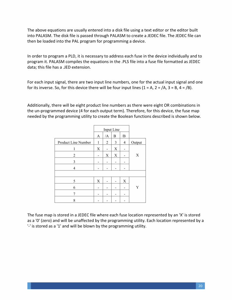
For each input signal, there are two input line numbers, one for the actual input signal and one for its inverse. So, for this device there will be four input lines (1 = A, 2 = /A, 3 = B, 4 = /B).
Additionally, there will be eight product line numbers as there were eight OR combinations in the un‐programmed device (4 for each output term). Therefore, for this device, the fuse map needed by the programming utility to create the Boolean functions described is shown below.
Input Line
A /A B /B
Product Line Number 1 2 3 4 Output
1 X - X -
X 2 - X X -
3 - - - -
4 - - - -
5 X - - X
Y 6 - - - -
7 - - - -
8 - - - -
The fuse map is stored in a JEDEC file where each fuse location represented by an 'X' is stored as a '0' (zero) and will be unaffected by the programming utility. Each location represented by a '‐' is stored as a '1' and will be blown by the programming utility.
21
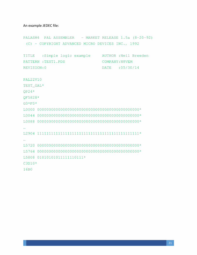
An example JEDEC file:
PALASM4 PAL ASSEMBLER - MARKET RELEASE 1.5a (8-20-92)
(C) - COPYRIGHT ADVANCED MICRO DEVICES INC., 1992
TITLE :Simple logic example AUTHOR :Neil Breeden
PATTERN :TEST1.PDS COMPANY:N8VEM
REVISION:0 DATE :05/30/14
PAL22V10
TEST_GAL*
QP24*
QF5828*
G0*F0*
L0000 00000000000000000000000000000000000000000000*
L0044 00000000000000000000000000000000000000000000*
L0088 00000000000000000000000000000000000000000000*
…
L2904 11111111111111111111111111111111111111111111*
…
L5720 00000000000000000000000000000000000000000000*
L5764 00000000000000000000000000000000000000000000*
L5808 01010101011111110111*
C3D10*
16B0
22
PALASM LANGUAGE GUIDE
Content copied from http://orion.ipt.pt/~fmbarros/ed/PALASM%20Language%20Guide.htm#Top
DESIGN WITH BOOLEAN EQUATIONS
A .PDS file using Boolean equations to specify a design consists of two or three sections: declarations, equations,
and optional simulation specifications. The declaration section is used to identify the design, list target device data,
and define string constants. The equation section defines the outputs in terms of inputs and feedback paths. It also
supports device‐specific configuration.
The vocabulary of .PDS files is given separately. The grammar and syntax for .PDS files with Boolean equations is also given separately. General comments about grammar and syntax issues follow.
Note that the first several lines of the grammar (TITLE, PATTERN, ..., DATE) are all optional. If the optional lines are omitted, warning messages will be generated. The information following these optional lines is limited to 24 characters.
The reserved word CHIP is required. The description is limited to 13 alphanumeric characters. The device name must designate a device supported by the software. The on-line databook (in PALASM2) shows which devices are supported. The names of the pins as they are used in the program follow. Traditional style dictates that the pin numbers be placed by the names using comment lines.
Some PLDs have internal global preset or reset lines which affect all the registers in the device. If the device being programmed has this feature (e.g., PAL22V10s), PALASM requires the definition of a phantom pin at the end of the pin definitions. For a 24 pin device, the phantom pin would be defined as a 25th pin. Typical names for the pin are global.rst or global.set which can then be used in the equations section, if desired. Omitting a phantom pin results in the warning "Not enough pins defined".
The STRING section is optional. It permits frequently used patterns to be replaced by a name. For example, a four-literal expression for the numeric value three could be declared as "ONE '/I3 * /I2 * I1 * I0'". Strings can contain other strings, but the references must not be recursive.
The section starting with the reserved word EQUATIONS is required. What follows is a set of Boolean equations which define the functions implemented by the PLD. The results can be combinational (designated with "="), synchronously registered (designated with ":="), or asynchronously latched (designated with "*="). The equations can span more than one line, but no single line may span more than 128 columns.
23
The permitted operations are the standard Boolean operators with normal precedence: NOT ("/"), AND ("*"), OR ("+"), and XOR (":+:"). Parentheses may be used to group terms.
The output can also be specified as being asserted low or asserted high. Outputs which are to be asserted low are preceded by a slash. For example, /Q2 = I2 + /I1 + I0 would be low when I2=1, I1=0, and I0=1. It would be high otherwise.
DESIGN WITH STATE MACHINES
PALASM allows state machine circuits to be descibed as either Mealy machines (outputs depend on both current
state and current inputs) or as Moore machines (outputs depend on just the current state). The specific syntax and
semantics for .PDS files with state machine design is given separately. Specific comments about the syntax and
semantics follow.
The declaration section follows the same rules as for a Boolean equation design.
The type of state machine to be implemented is specified by using the reserved word MEALY_MACHINE or MOORE_MACHINE.
The global defaults provide a concise way of specifying circuit behavior for cases not explicitely defined in later parts of the design specification. Default state transitions can be specified in one of three ways:
DEFAULT_BRANCH <state name>
DEFAULT_BRANCH HOLD_STATE
DEFAULT_BRANCH NEXT_STATE
The first defaults to the specified state, the second to the same state, and the third to the next state appearing in the design description.
Default outputs can also be specified as shown below.
OUTPUT_HOLD <output pin list>
DEFAULT_OUTPUT <output pin values>
24
In the first case, the list specifies output pins which do not change. In the second case, the output pins go to the specified values. The character '%' preceding a pin name in a pin list denotes a "don't care" output while a '/' preceding a pin name indicates a low output value.
The optional state assignment section equates state names with a unique set of state variable values. The variable values are stored in registers. The syntax of state assignments is
<state name> = <var1val> * <var2val> * .... * <varNval>
The character '/' precedes variables which are low. State names must be unique and may contain up to 14 characters. By assigning your states values, you may get a better design than by allowing Palasm to do the assignment for you.
The state equations define the state transitions of the state machine. The syntax of each state equation is
<current state name> := <condition1> -> <next state 1>
+ <condition2> -> <next state 2>
...
+ <conditionN> -> <next state N>
+-> <local default state>
The current state and next state names are those defined in the state assignment section. The conditions are defined in the condition section. The local default state line is optional. When present, the local default state overrides any global default state definition. When absent, the global default is used. An unconditional state transition should use the reserved word VCC as the condition.
An output equation for each state equation is required if OUTPUT_HOLD (in PLS and PROSE designs) or DEFAULT_OUTPUT is specified in the design. Otherwise, the output equations are optional. If the outputs are the same as the state, do not specify output equations. Registered Mealy outputs take on new values one clock cycle after a new state is reached. All others are valid when the new state is reached. For Mealy machines, the output syntax is
<state name>.OUTF <OP> <condition1> -> <output list 1>
+ <condition2> -> <output list 2>
...
+ <conditionN> -> <output list N>
+-> <local output defaults>

25
For Moore machines, the syntax is
<state name>.OUTF <OP> <output list>
where <OP> is again either := for registered outputs or = for combinational outputs. The syntax of the output list is
<pin label> * <pin label> * ... * <pin label>
where the number of labels in the list is one or more.
The condition section is used to define unique input value combinations. These conditions are then used in the state transition section. The condition section begins with the reserved word CONDITIONS and is followed by a list of definitions with the following syntax:
<condition name> = <input Boolean expression>
The condition name can contain up to 14 characters and must be unique. The input Boolean expression must use input names as defined in the pin list or string section and it must be unique. Conditions involving only one input do not need to be explicitely defined. Care should be taken to define conditions so that only one is true at any given time.
SIMULATION
PALASM provides an event‐driven simulator for PLD design. The simulation is specified as an optional part of the
.PDS design file. It begins with the reserved word SIMULATION and is followed by simulation commands. The
results of the simulation are stored in two files: the .HST file which contains a complete history of the simulation
and the .TRF file which contains a trace of signals specified by the TRACE_ON command.
The next section covers the syntax and meaning of the simulation commands as well as the interpretation of simulation results. A brief simulation command summary is also available.
SIMULATION COMMANDS
The simulation commands can be divided into three categories: value, control, and verification.
VALUE SIMULATION COMMANDS
The value commands set simulation values. The general syntax is
26
COMMAND <List of pin names and values>
The list of pin names consists of the name of one or more pins, possibly qualified by the '/' character. Names are separated by blank spaces. The '/' indicates the signal is low or complemented. Its absence indicates the signal is high or un-complemented. A '/' in the pin list will complement a '/' in the CHIP declaration section.
The PRLDF command is used to initialize the values of registers which can be loaded with a value at power-up (preloaded). For example, let P1, P2, and P3 be the output pins associated with registers which are to be preloaded with 1, 0, and 1, respectively. This would be stated in the simulation as
PRLDF P1 /P2 P3
If the device cannot be preloaded, the command simply initializes the registers. The Xeltek programmer in the EE department does not support preloading.
The SETF command specifies input signal values. For example, let I1, I2, and I3 be pins associated with input signals which are to be set to 0, 1, and 1, respectively. This would be stated in the simulation as
SETF /I1 I2 I3
The inputs will retain the values until explicitly changed. Until a value is specified, input values default to 'undefined'. SETF can be used with clock input pins.
The CLOCKF command generates a clock pulse signal on the specified clock input pins. The pulse goes low-high-low. For example, consider the clock signal CLK0. It would be pulsed by
CLOCKF CLK0
CONTROL SIMULATION COMMANDS
The control commands permit repetitive and selective execution of commands based on condition evaluation. The
conditions for the WHILE and IF commands make use of the relational operators< , >, =, <=, and >=. The conditional
expressions may not contain nested parentheses.
The syntax of the FOR command is
FOR <index var> := <start> TO <end> DO
BEGIN
27
<command list>
END
An example of the FOR command follows:
FOR J:=1 TO 8 DO
BEGIN
SETF /I0 I1
CLOCKF CLK0
END
FOR loops may be nested. The value of <start> must be less than that of <end> and both must be non-negative. If the limits are equal, the loop is NOT executed.
The syntax of the WHILE command is
WHILE <condition> DO
BEGIN
<command list>
END
An example WHILE statement:
WHILE (J <= 7) DO
BEGIN
SETF I0 I1
CLOCKF CLK1
J := J + 1
END
WHILE loops may be nested. The <condition> may be either a numeric comparison or Boolean evaluation.
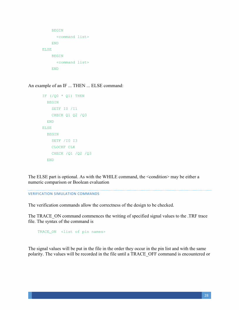
The syntax of the IF...THEN...ELSE command is
IF <condition> THEN
28
BEGIN
<command list>
END
ELSE
BEGIN
<command list>
END
An example of an IF ... THEN ... ELSE command:
IF (/Q0 * Q1) THEN
BEGIN
SETF I0 /I1
CHECK Q1 Q2 /Q3
END
ELSE
BEGIN
SETF /I0 I3
CLOCKF CLK
CHECK /Q1 /Q2 /Q3
END
The ELSE part is optional. As with the WHILE command, the <condition> may be either a numeric comparison or Boolean evaluation
VERIFICATION SIMULATION COMMANDS
The verification commands allow the correctness of the design to be checked.
The TRACE_ON command commences the writing of specified signal values to the .TRF trace file. The syntax of the command is
TRACE_ON <list of pin names>
The signal values will be put in the file in the order they occur in the pin list and with the same polarity. The values will be recorded in the file until a TRACE_OFF command is encountered or
29
the simulation ends. TRACE_OFF has no arguments. Different signals can be traced by specifying them in a TRACE_ON command which follows a TRACE_OFF.
The CHECK command compares simulation values with expected values. The syntax of the command is
CHECK <list of pin names and values>
The list of pin names consists of the name of one or more pins, possibly qualified by the '/' character. Names are separated by blank spaces. The '/' indicates the signal is low or complemented. Its absence indicates the signal is high or un-complemented.
For example, suppose that at a given point in a simulation, the pins P1, P2, and P3 are to have the values 0, 1, and 0, respectively. This would be specified as
CHECK /P1 P2 /P3
30
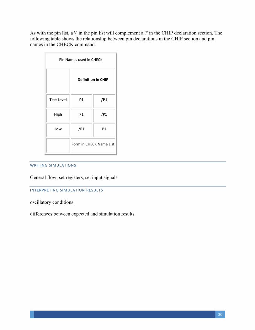
As with the pin list, a '/' in the pin list will complement a '/' in the CHIP declaration section. The following table shows the relationship between pin declarations in the CHIP section and pin names in the CHECK command.
Pin Names used in CHECK
Definition in CHIP
Test Level P1 /P1
High P1 /P1
Low /P1 P1
Form in CHECK Name List
WRITING SIMULATIONS
General flow: set registers, set input signals
INTERPRETING SIMULATION RESULTS
oscillatory conditions
differences between expected and simulation results
31
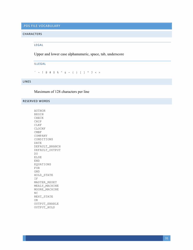
.PDS FILE VOCABULARY
CHARACTERS
LEGAL
Upper and lower case alphanumeric, space, tab, underscore
ILLEGAL
` ~ ! @ # $ % ^ & - { } [ ] " ? < >
LINES
Maximum of 128 characters per line
RESERVED WORDS
AUTHOR BEGIN CHECK CHIP CLKF CLOCKF CMBF COMPANY CONDITIONS DATE DEFAULT_BRANCH DEFAULT_OUTPUT DO ELSE END EQUATIONS FOR GND HOLD_STATE IF MASTER_RESET MEALY_MACHINE MOORE_MACHINE NC NEXT_STATE OR OUTPUT_ENABLE OUTPUT_HOLD
32
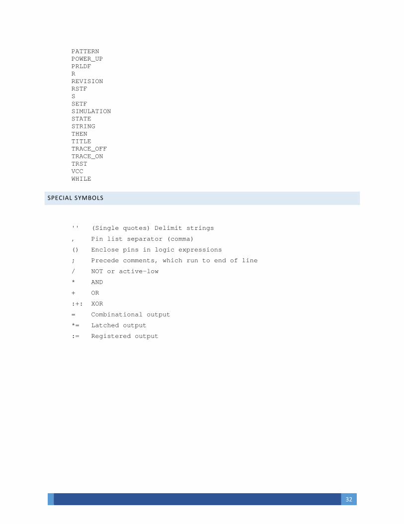
PATTERN POWER_UP PRLDF R REVISION RSTF S SETF SIMULATION STATE STRING THEN TITLE TRACE_OFF TRACE_ON TRST VCC WHILE
SPECIAL SYMBOLS
'' (Single quotes) Delimit strings
, Pin list separator (comma)
() Enclose pins in logic expressions
; Precede comments, which run to end of line
/ NOT or active-low
* AND
+ OR
:+: XOR
= Combinational output
*= Latched output
:= Registered output
33
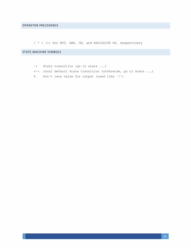
OPERATOR PRECEDENCE
/ * + :+: for NOT, AND, OR, and EXCLUSIVE OR, respectively
STATE MACHINE SYMBOLS
-> State transition (go to state ...)
+-> Local default state transition (otherwise, go to state ...)
% Don't care value for output (used like '/')
34
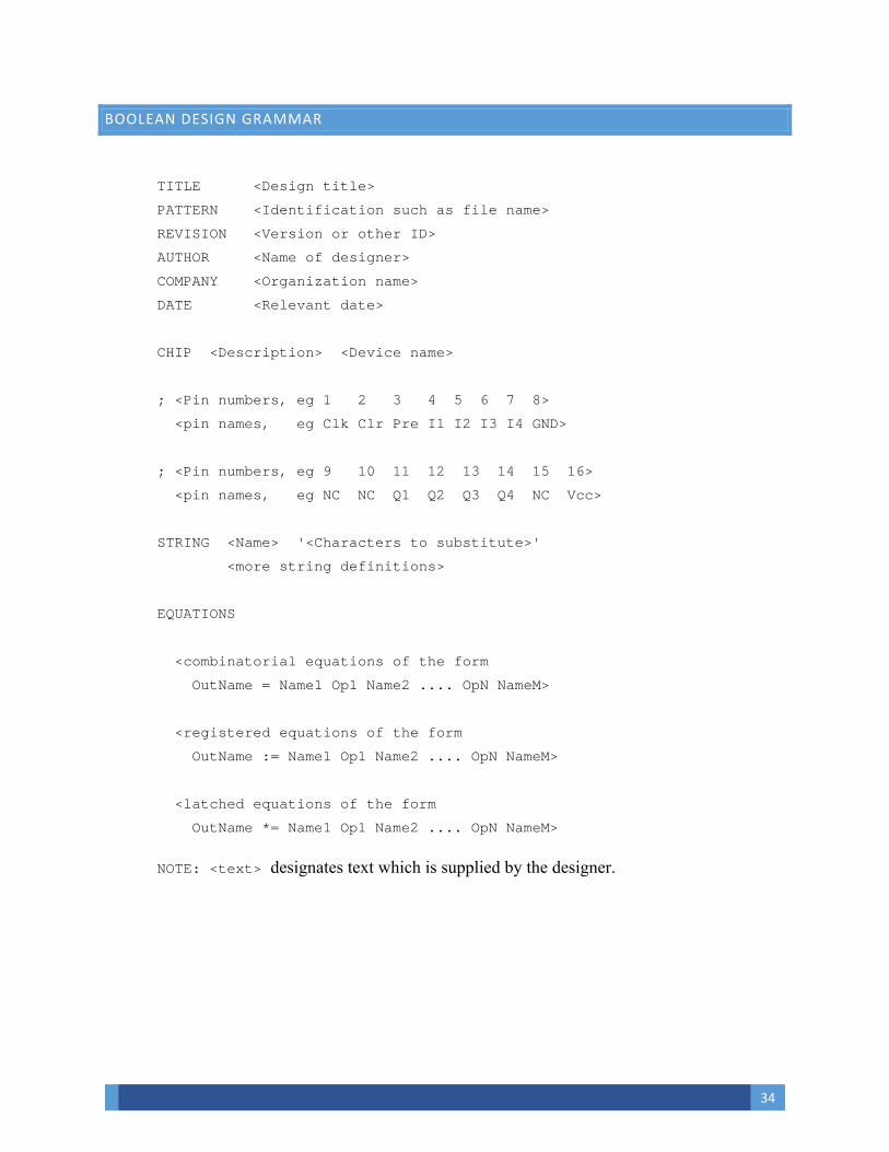
BOOLEAN DESIGN GRAMMAR
TITLE <Design title>
PATTERN <Identification such as file name>
REVISION <Version or other ID>
AUTHOR <Name of designer>
COMPANY <Organization name>
DATE <Relevant date>
CHIP <Description> <Device name>
; <Pin numbers, eg 1 2 3 4 5 6 7 8>
<pin names, eg Clk Clr Pre I1 I2 I3 I4 GND>
; <Pin numbers, eg 9 10 11 12 13 14 15 16>
<pin names, eg NC NC Q1 Q2 Q3 Q4 NC Vcc>
STRING <Name> '<Characters to substitute>'
<more string definitions>
EQUATIONS
<combinatorial equations of the form
OutName = Name1 Op1 Name2 .... OpN NameM>
<registered equations of the form
OutName := Name1 Op1 Name2 .... OpN NameM>
<latched equations of the form
OutName *= Name1 Op1 Name2 .... OpN NameM>
NOTE: <text> designates text which is supplied by the designer.
35
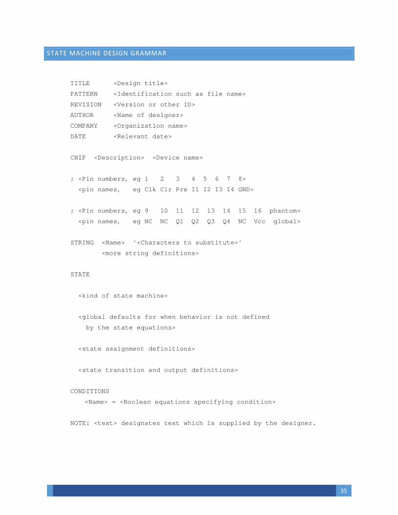
STATE MACHINE DESIGN GRAMMAR
TITLE <Design title>
PATTERN <Identification such as file name>
REVISION <Version or other ID>
AUTHOR <Name of designer>
COMPANY <Organization name>
DATE <Relevant date>
CHIP <Description> <Device name>
; <Pin numbers, eg 1 2 3 4 5 6 7 8>
<pin names, eg Clk Clr Pre I1 I2 I3 I4 GND>
; <Pin numbers, eg 9 10 11 12 13 14 15 16 phantom>
<pin names, eg NC NC Q1 Q2 Q3 Q4 NC Vcc global>
STRING <Name> '<Characters to substitute>'
<more string definitions>
STATE
<kind of state machine>
<global defaults for when behavior is not defined
by the state equations>
<state assignment definitions>
<state transition and output definitions>
CONDITIONS
<Name> = <Boolean equations specifying condition>
NOTE: <text> designates text which is supplied by the designer.
36
SIMULATION COMMANDS SUMMARY
VALUE COMMANDS
PRLDF Initialize preloadable register outputs
SETF Specify input values
CLOCKF Generate clock signal for clock input
CONTROL COMMANDS
FOR...TO...DO
WHILE...DO
IF...THEN...ELSE
The syntax and use of these three commands is comparable to computer languages like BASIC, Modula-2, etc.
VERIFICATION COMMANDS
CHECK Compare expected and simulated signal values
TRACE_ON Specifies signals for .TRF file and recording interval
TRACE_OFF
Copyright © 1991, 1996 NDSU EE Dept.
Content copied from http://orion.ipt.pt/~fmbarros/ed/PALASM%20Language%20Guide.htm#Top
37
38
39
40
41
42
43
44
45
PLD DESIGN METHODOLOGY
46
47
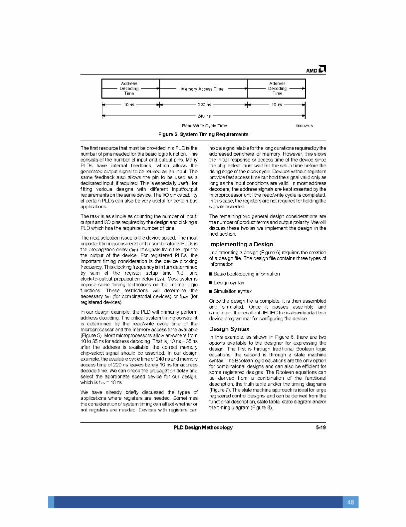
48
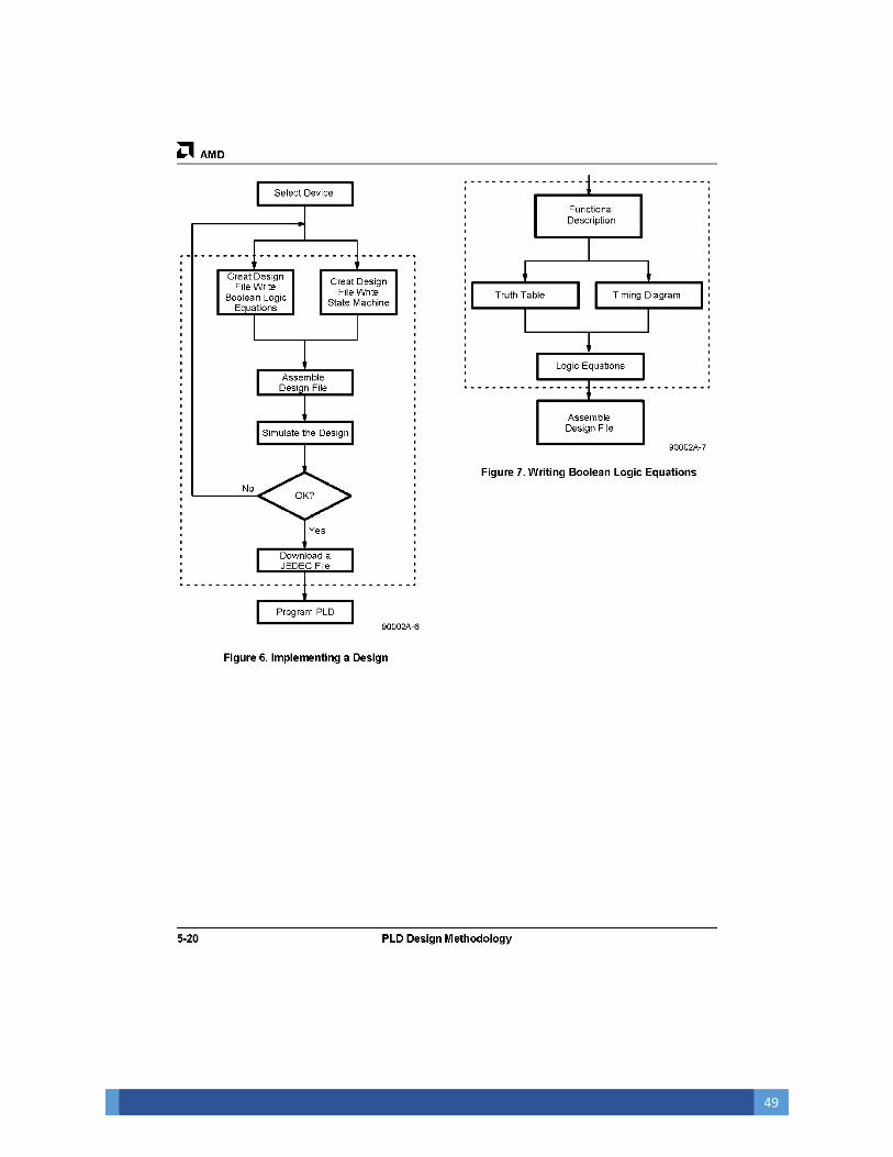
49
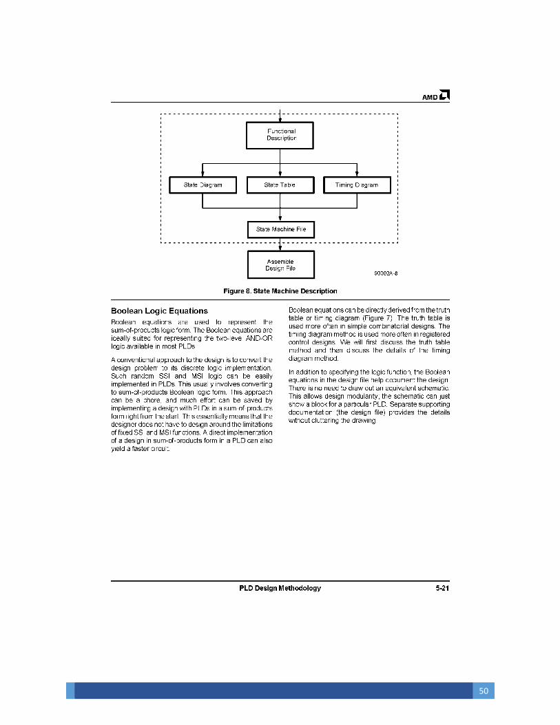
50
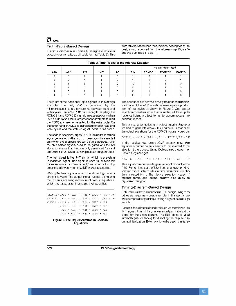
51
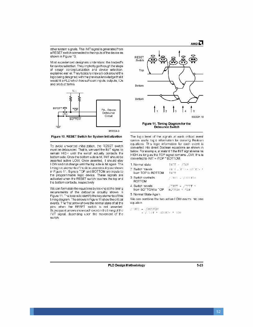
52
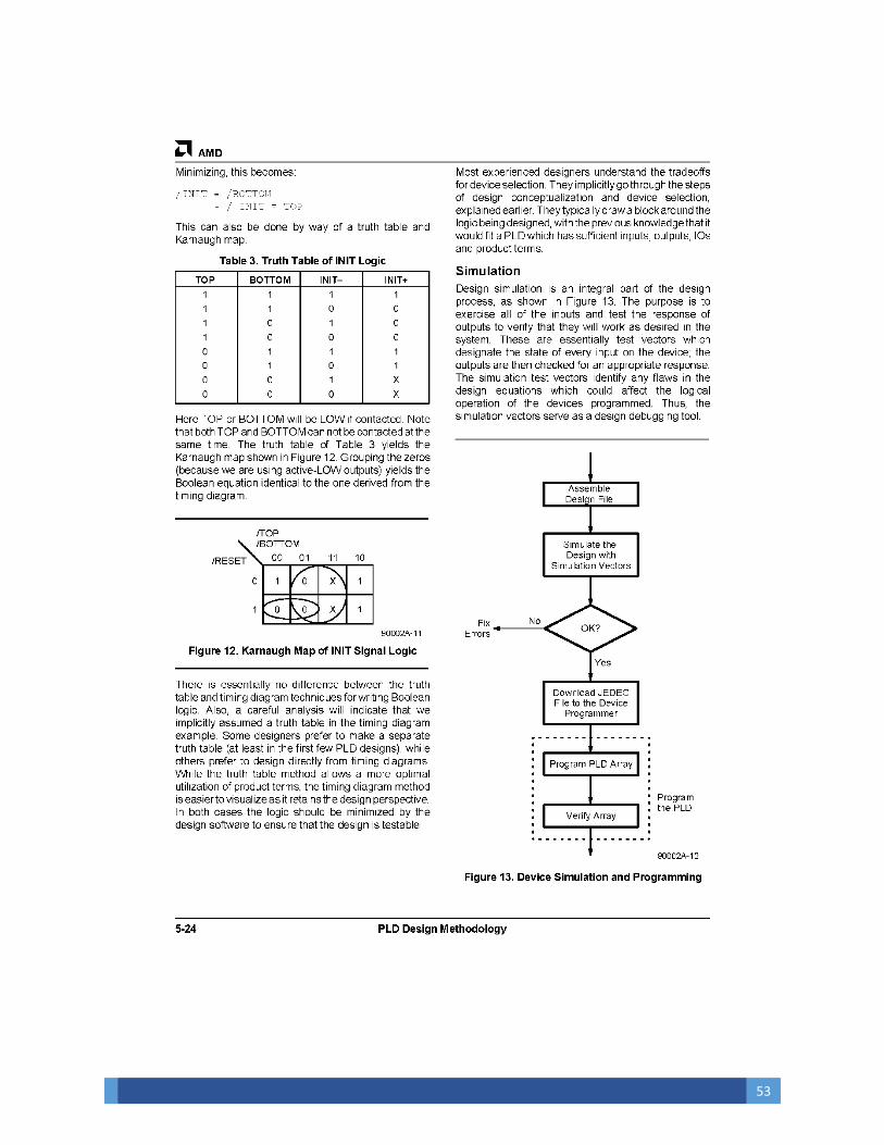
53

54
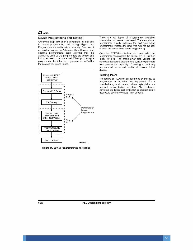
55
56
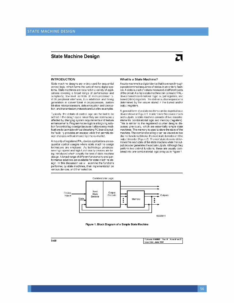
STATE MACHINE DESIGN
57
58
59

60
61
62
63
64

65
66
67
68
69
REGISTERED LOGIC DESIGN
70
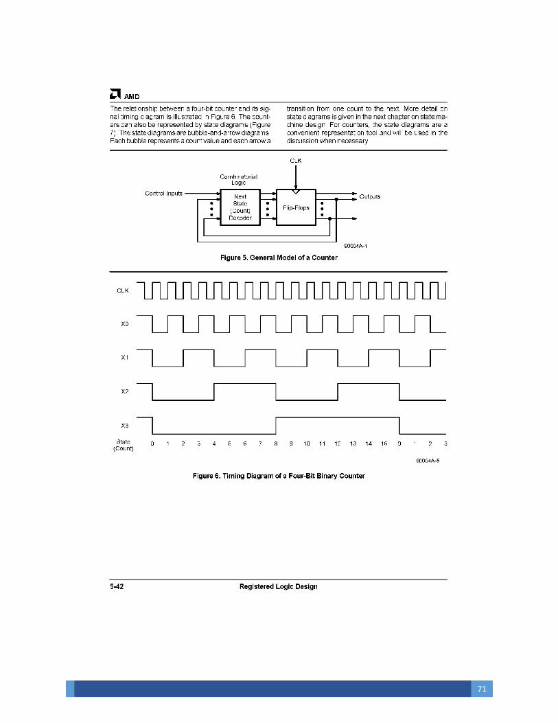
71
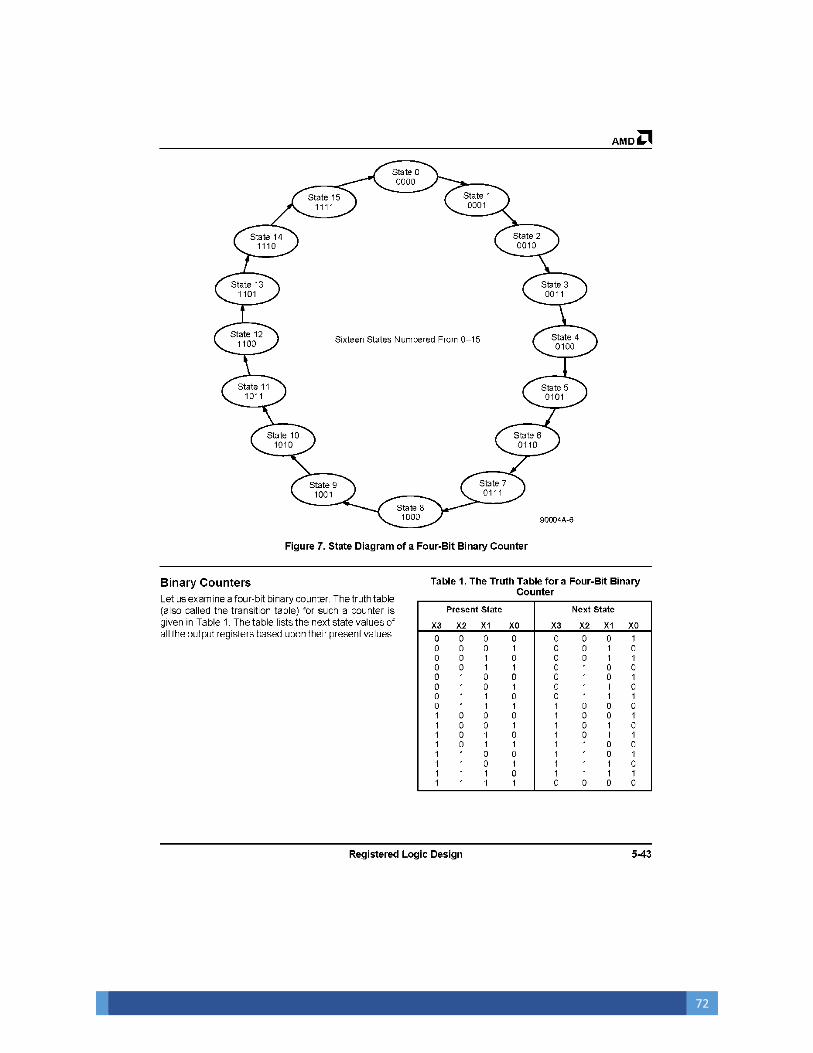
72
73
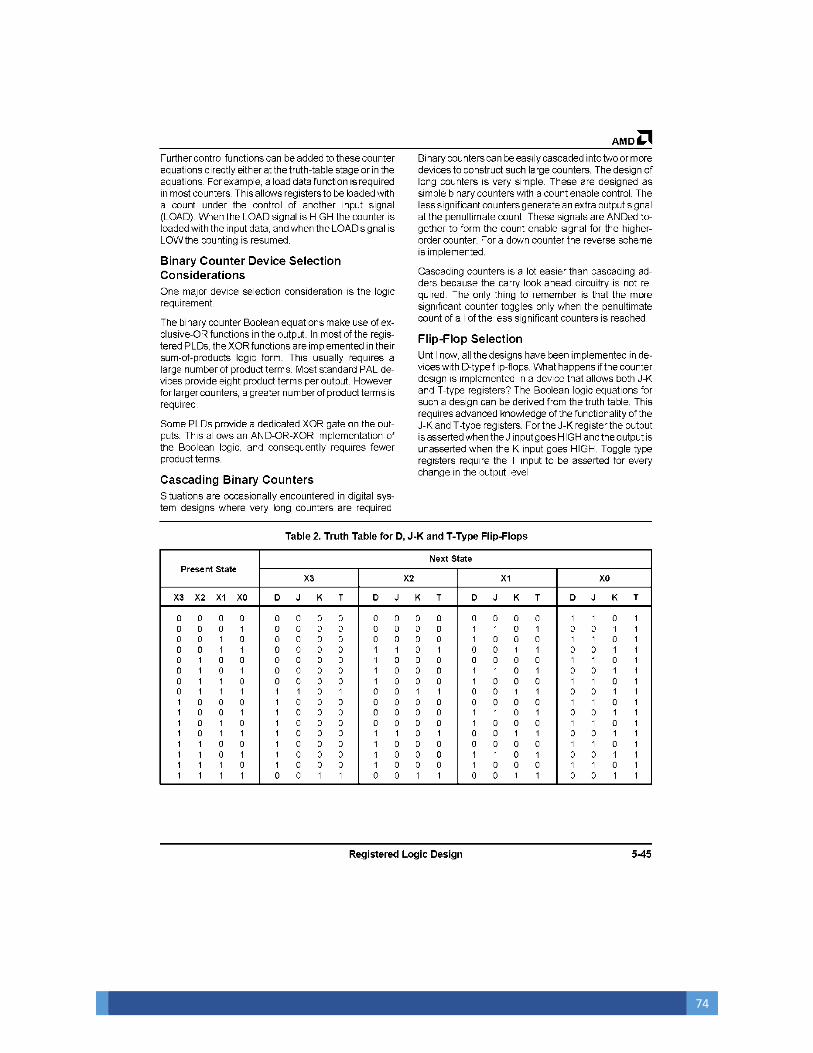
74
75
76
77
78
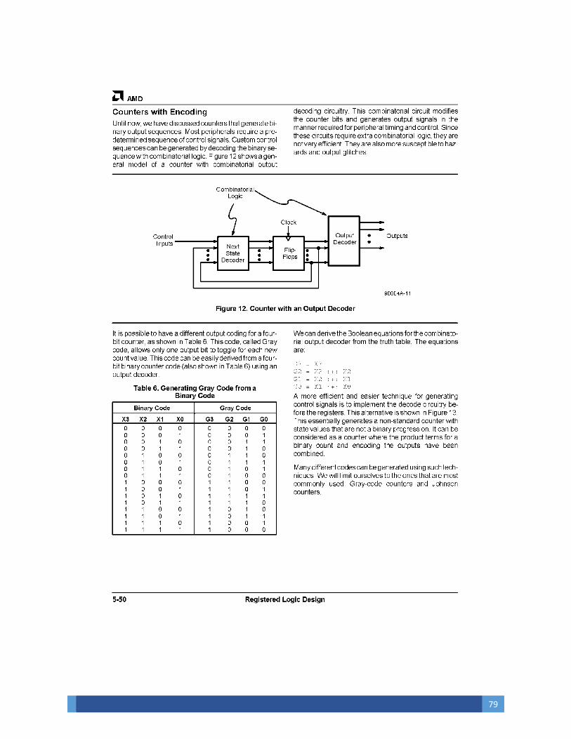
79
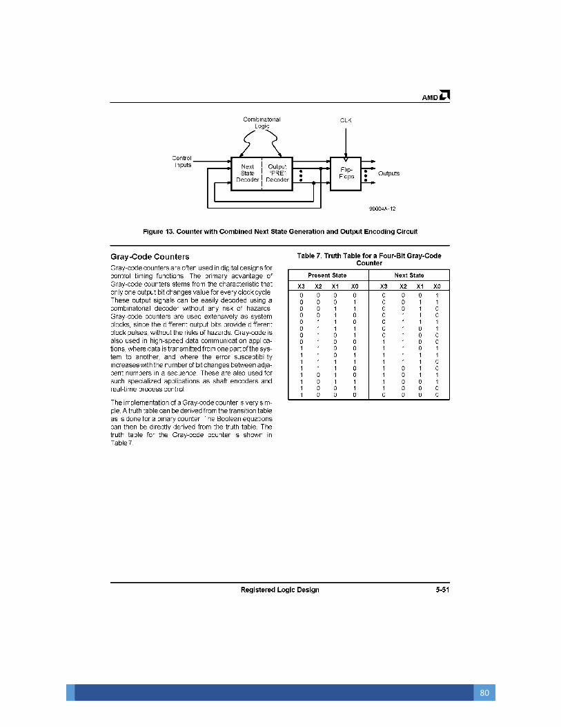
80
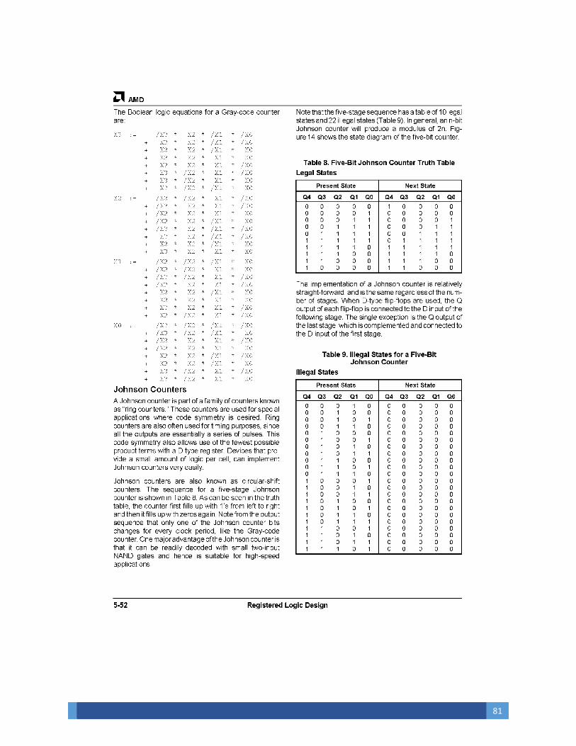
81
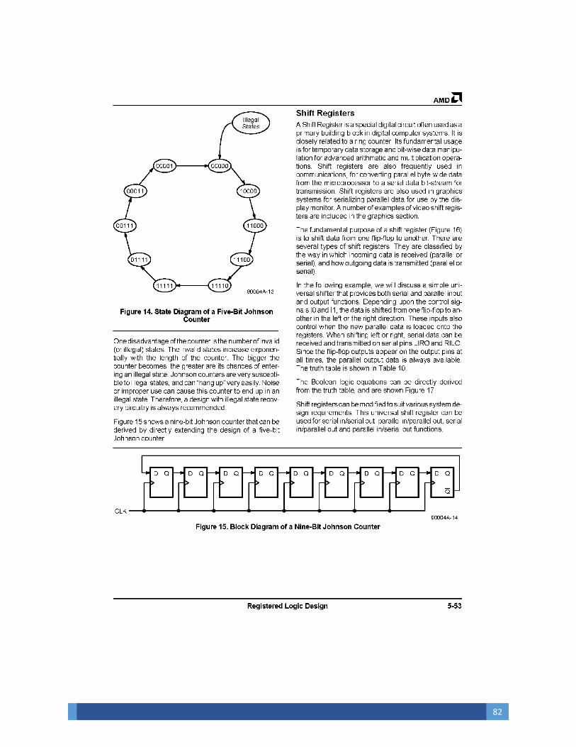
82
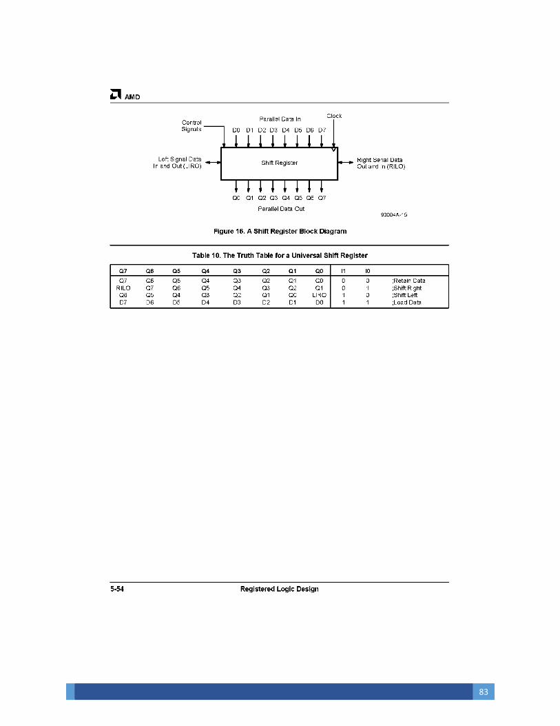
83
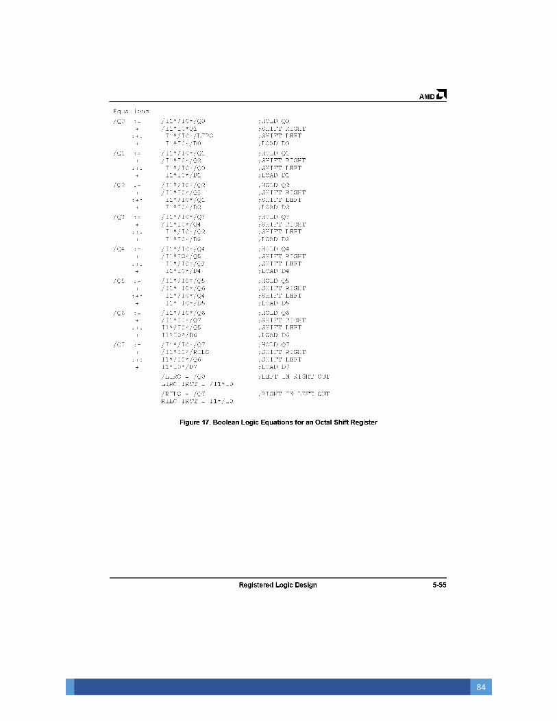
84
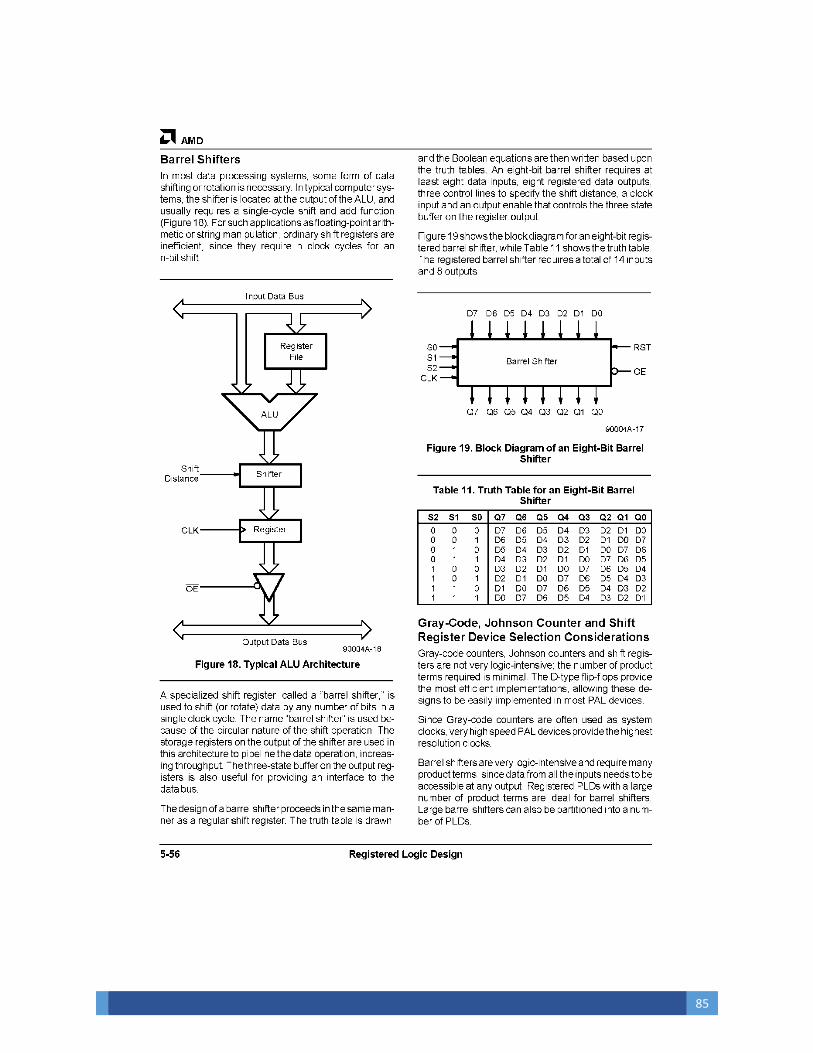
85
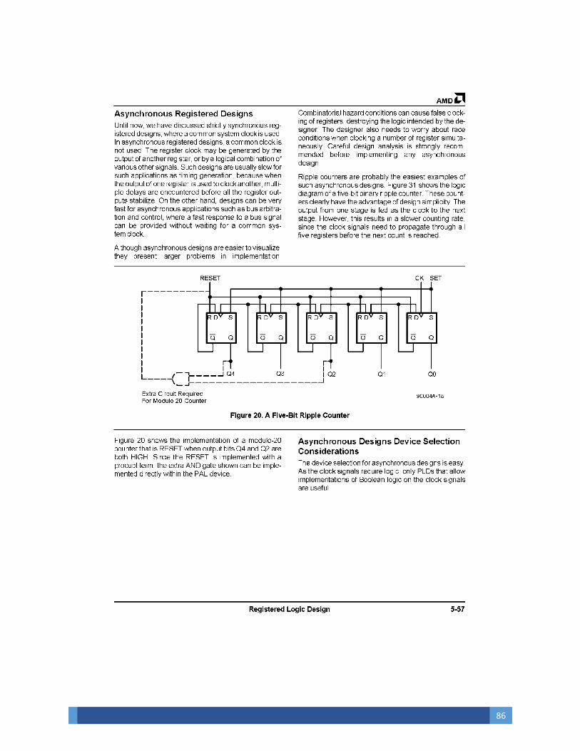
86
87
88
89
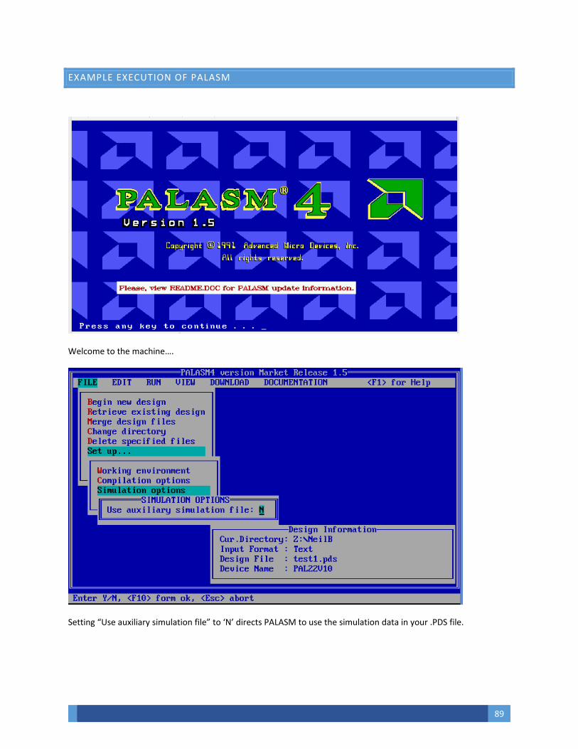
EXAMPLE EXECUTION OF PALASM
Welcome to the machine….
Setting “Use auxiliary simulation file” to ‘N’ directs PALASM to use the simulation data in your .PDS file.
90
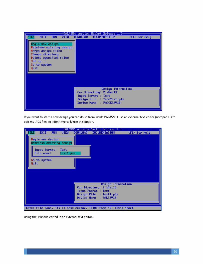
If you want to start a new design you can do so from inside PALASM. I use an external text editor (notepad++) to
edit my .PDS files so I don’t typically use this option.
Using the .PDS file edited in an external text editor.
91
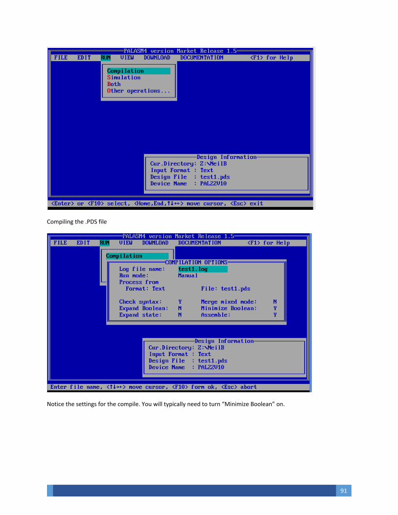
Compiling the .PDS file
Notice the settings for the compile. You will typically need to turn “Minimize Boolean” on.

92
It compiled!
Running a simulation of the design.
93
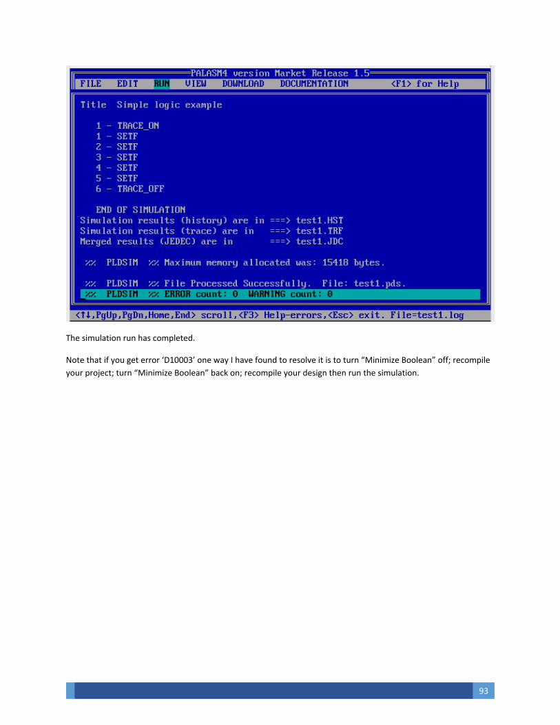
The simulation run has completed.
Note that if you get error ‘D10003’ one way I have found to resolve it is to turn “Minimize Boolean” off; recompile
your project; turn “Minimize Boolean” back on; recompile your design then run the simulation.
94
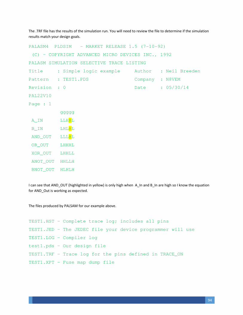
The .TRF file has the results of the simulation run. You will need to review the file to determine if the simulation
results match your design goals.
PALASM4 PLDSIM - MARKET RELEASE 1.5 (7-10-92)
(C) - COPYRIGHT ADVANCED MICRO DEVICES INC., 1992
PALASM SIMULATION SELECTIVE TRACE LISTING
Title : Simple logic example Author : Neil Breeden
Pattern : TEST1.PDS Company : N8VEM
Revision : 0 Date : 05/30/14
PAL22V10
Page : 1
ggggg
A_IN LLHHL
B_IN LHLHL
AND_OUT LLLHL
OR_OUT LHHHL
XOR_OUT LHHLL
ANOT_OUT HHLLH
BNOT_OUT HLHLH
I can see that AND_OUT (highlighted in yellow) is only high when A_In and B_In are high so I know the equation
for AND_Out is working as expected.
The files produced by PALSAM for our example above.
TEST1.HST - Complete trace log; includes all pins
TEST1.JED - The JEDEC file your device programmer will use
TEST1.LOG - Compiler log
test1.pds - Our design file
TEST1.TRF - Trace log for the pins defined in TRACE_ON
TEST1.XPT - Fuse map dump file

Version History:
V1.5 – Initial Release
V1.6 – Addition content and editiing