Embed Size (px)
Citation preview

Programming the Adapteva Epiphany 64-coreNetwork-on-chip CoprocessorAnish Varghese, Bob Edwards, Gaurav Mitra, Alistair P Rendell
Research School of Computer ScienceAustralian National University
Canberra, AustraliaEmail: [email protected], [email protected],
[email protected], [email protected]
Abstract—In the construction of exascale computing systemsenergy efficiency and power consumption are two of the majorchallenges. Low-power high performance embedded systems areof increasing interest as building blocks for large scale high-performance systems. However, extracting maximum perfor-mance out of such systems presents many challenges. Various as-pects from the hardware architecture to the programming modelsused need to be explored. The Epiphany architecture integrateslow-power RISC cores on a 2D mesh network and promises upto 70 GFLOPS/Watt of processing efficiency. However, with just32 KB of memory per eCore for storing both data and code, andonly low level inter-core communication support, programmingthe Epiphany system presents several challenges. In this paperwe evaluate the performance of the Epiphany system for avariety of basic compute and communication operations. Guidedby this data we explore strategies for implementing scientificapplications on memory constrained low-powered devices such asthe Epiphany. With future systems expected to house thousandsof cores in a single chip, the merits of such architectures as apath to exascale is compared to other competing systems.
Index Terms—Network-on-chip ; Epiphany ; Stencil ; Paral-lella ; Matrix-Matrix Multiplication
I. INTRODUCTION
The Epiphany architecture comprises a low power, multi-core, scalable, parallel, distributed shared memory embed-ded system created by Adapteva[1]. The Epiphany IV 64-core Network-on-chip (NoC) coprocessor contains 64 cores(referred to as eCores) organized in a 2D mesh with futureversions expected to house up to 4096 eCores. The ParallellaSystem-on-module (SoM) board[1] combines the Epiphany IVchip with a host ARM processor housed in a Zynq System-on-chip. An earlier development prototype of the Parallellauses an FPGA mezzanine “daughter” card (FMC) housing theEpiphany IV, attached to a ZedBoard [2]. In this paper wereport our evaluation of the hardware characteristics and soft-ware environment of the Epiphany system from the perspectiveof an application program developer using the ZedBoard andFMC daughter card setup.
To assess the performance of the Epiphany system weimplement a stencil based scientific application kernel anda parallel matrix multiplication kernel. Stencil kernels applyregular operations on a grid, and are common to a wide rangeof high performance computing applications, and have similarcharacteristics to other applications such as image processing.
They require good floating point performance but also fastcommunications. Parallelization is usually via domain de-composition with communications primarily between adjacentdomains. Such applications might be expected to map well tothe 2D mesh topology of the Epiphany coprocessor.
Multiplication of matrices is a fundamental operation whichis used in many scientific applications. Here, we implementand extend the parallel matrix multiplication algorithm de-scribed by Sapir [3] which involves data communicationbetween neighbouring cores following Cannon’s algorithm[4]. The relatively small memory per core presents somechallenges in implementing this, necessitating careful usageof available memory buffer space for communication betweencores.
In the following sections we give a brief overview of theEpiphany system and the programming model it supports. Wethen discuss how this impacts on program design. In SectionV we outline micro-benchmarks used to assess the basicperformance of the Epiphany coprocessor. Section VI detailsthe parallel stencil implementation along with performanceresults. Section VII details the parallel matrix multiplicationimplementation along with performance results. Section VIIIhighlights related work and contrasts the Epiphany with simi-lar many-core energy efficient systems. Conclusions and futurework are outlined in Section IX.
II. SYSTEM ARCHITECTURE
Both the Parallella and the prototype ZedBoard consist of aZynq SoC, shared memory and the Epiphany NoC coprocessoras shown in Figure 1.
The Xilinx Zynq 7000 series SoC contains a dual-core ARMCortex-A9 CPU running at 800 MHz on the Parallella and667 MHz on the ZedBoard, with standard on-chip peripheralssuch as USB 2.0, Ethernet, UART, MIO, AXI BUS, GPIO,HDMI, JTAG etc. It also contains a Field Programmable GateArray (FPGA) which is used to implement the “Glue-Logic”and eLink protocol required to interface with the Epiphanycoprocessor. In addition, the FPGA implements the AXImaster interface, AXI slave interface and a HDMI controller.
The Epiphany NoC has a 2D array of eCores connected toeach other by a mesh network-on-chip. Each eCore consistsof a RISC CPU, 32 KB of local scratchpad memory, a Direct
arX
iv:1
410.
8772
v1 [
cs.A
R]
30
Oct
201
4

Fig. 1: Adapteva Epiphany System
Memory Access (DMA) engine, and a network interface toan eMesh router. No cache is present. Each eMesh routerprovides three network communication channels; an on-chipwrite network (in blue), an off-chip write network (in green)and a read request network (in red). The eCore CPU issuper-scalar and can execute two floating-point operations anda 64-bit memory load/store operation in every clock cycle.Scratchpad memory can theoretically provide up to 32 Bytesper clock cycle of bandwidth.
The Parallella SoM has 1 GB of DDR3 RAM, while theZedBoard has 512 MB. The DRAM is partitioned such thatLinux running on the ARM Cortex-A9 CPU has its ownprivate O/S memory and the rest is accessible by both theARM and Epiphany. Shared memory access for the Epiphanyis handled by an eLink interface via the AXI bus and memorycontroller on the Zynq SoC. The Epiphany has a flat andunprotected memory map. Each eCore can address its localSRAM, other eCores’ SRAMs and shared off-chip DRAM.
III. PROGRAMMING MODEL
The Epiphany chip can be programmed using C, and hasan SDK [1] that provides some basic programming primitivesto facilitate writing parallelized C code for this architecture.Some of the key features of the SDK are:
• Workgroup model: To program the eCores, workgroupsare created by specifying the number of rows andcolumns of nodes and the location of the starting nodeof the group. The SDK provides functions to determinethe ID and location of neighbouring eCores.
• Memory addressing: All eCores share the same addressspace and it is possible to read and write directly tothe local memory of another eCore. The SDK providesfunctions to obtain the global address of a memorylocation in another eCore’s local memory facilitating datatransfer between the nodes.
• Communication between eCores: The SDK provides APIsto transfer blocks of data between nodes and to the sharedmemory. These can be achieved by using either the CPUor the DMA engine. Two DMA channels are availablein each node supporting both non-blocking and blockingDMA transfers.
• Barriers: The SDK provides functions for setting syn-chronization points and barriers in the program.
• Hardware Mutex: Mutexes are available to ensure mutualexclusion while accessing shared resources. The work-group defines a memory location on the chip as the mutexobject. The SDK provides functions to enable the eCoresto utilize the mutex object.
• Event Timers: Each eCore has two event timers that canbe configured to independently monitor key events withinthe node such as clock counter, watchdog timing etc. Thiscan be used to count the number of clock cycles whichhave elapsed during execution of a block of code.
The steps required to execute a program are:1) Host program creates a workgroup by specifying the
number of rows and columns required and the positionof the start node in the group.
2) Host resets all the nodes and loads the device-side exe-cutable image into each eCore.
3) Host signals all the eCores in the workgroup to startexecution
4) Host communicates with each eCore either by accessingthe core’s local memory or using the shared memory.
5) Once the execution is complete, the host is signalled. Thehost reads the result either directly from each eCore’slocal memory or from the shared memory.
IV. PROGRAMMING CONSIDERATIONS
The Epiphany eCore architecture presents some interest-ing challenges to implementing high performance numericalcodes. The main limitation is the relatively small 32KBytesof local RAM per eCore which must be divided betweenprogram code, data and stack. Although each eCore has accessto the entire 32-bit address space, performance drops off whenaccessing non-local memory. Within each eCore the suppliedlinker scripts allow the programmer to control which parts ofthe code and data are to reside in which specific bank of localmemory and which parts are to be located in slower off-chipshared memory.
In its current form the Epiphany eCore does not includehardware support for integer multiply, floating point divideor any double-precision floating point operations. This designdecision frees up silicon for other uses, e.g. for additionalcores. Obviously the implication of this varies from applicationto application.
2

Maximum floating-point performance is achieved wheneach eCore is performing a stream of Fused-Multiply-Add(FMADD) instructions with simultaneous 64-bit load or storeoperations in each clock cycle. At 600MHz on a 64-coreEpiphany this corresponds to a peak of 76.8 single-precisionGFLOPS. The ability of the compiler to optimise code andachieve this is another matter.
A. Program Structure
The development environment requires (at least) two Cprograms to be written: one for the host CPU and one ormore “kernels” for running on the eCore nodes.
An application code would typically perform all of itsinitialization and outer loops on the host CPU, with the inner-most, numerical-intensive, loops running as kernels on theEpiphany eCore nodes. Lesser-used library functions requiredby the kernel can be located in slower, but more abundant,shared-memory.
B. Overcoming Memory Limitations
As indicated previously, the local eCore memory is imple-mented as four banks of 8KBytes each. Maximum perfor-mance can be obtained only when code is fetched from onebank whilst load/store and DMA operations are occurring toother banks.
This further restricts code size to 8 or 16KBytes, or between2k and 8k instructions (depending on mix of 16-bit and 32-bitinstruction words). The programmer needs to carefully allocatethe use of these four local memory banks in order to achievethe best performance.
For example, the programmer could allocate one bank oflocal memory for code, two for data (“data1” and “data2”) andone for the stack and local variables. With such an arrangementthe code can process data to/from “data 1”, while using DMAto move data in/out of “data 2”. When the processing andDMA are complete, the code can then go on to process “data2” while using DMA to move result data out and new inputdata into “data 1”.
Adding further pressure on limited memory, branching (eg.in loops) costs 3 cycles, so should be avoided where possibleby “unrolling” inner loops. However unrolling loops comesat a cost to code size. With such small amounts of memoryavailable for code, it is necessary to finely tune the degree towhich loops are unrolled. Directives to the C compiler can beused to determine the degree of loop unrolling.
Instructions can, however be fetched from the local memoryof other eCores. Thus a novel approach may be to locatesmaller fragments of non-innermost-loop code in unused por-tions of banks of local memory of eCores within a row. Thiscode could then be executed, when required, with contentiononly between the eCores in that row. This would result in lesscontention for eMesh bandwidth than if all the eCores wereexecuting code out of external shared memory.
C. Hardware/Software Operation
Codes for array processing often make use of product termsin array indices, for example, to calculate row offsets. Without
hardware support for integer multiplication it is desirableto iterate through array elements in a regular matter usingincremented offsets. Similarly where possible floating-pointdivide operations should be removed from inner loops orminimized. In both cases these are optimisations that canusually be carried out by a compiler.
In terms of the current lack of support for double-precisionfloating point arithmetic, there is really no sensible work-around. However, there is increasing evidence to suggest thatfor many calculations careful use of single precision floatingpoint is sufficient [5], [6]. Also in the case of the Parallellaand other Epiphany platforms, the dual-core ARM Cortex-A9 CPUs on the Zynq chip provide high-performance double-precision Vector Floating Point Units (VFPU), so codes withhigh single-precision requirements and more modest double-precision requirements may fit the Zynq-Epiphany combina-tion well.
V. PERFORMANCE EXPERIMENTS
Experimental Platform: A ZedBoard [2] evaluation mod-ule containing a Xilinx Zynq 7000 SoC XC7Z020-CLG484-1with a daughter card [1] housing the Epiphany-IV 64-core28nm (E64G401) was used for all experiments. The dual-coreARM Cortex-A9 present on the Zynq SoC runs at 667 MHzand the Epiphany eCores run at 600 MHz each. The boardhas 512 MB of DDR3 RAM which has 480 MB allocatedas ARM Linux O/S private memory and 32 MB allocated asshared memory between ARM Linux and Epiphany eCores.
Compilers and Tools: The Epiphany SDK version 5.13 wasused to perform all experiments. The ARM Cortex-A9 runsthe Linux kernel version 3.3.0 and the Linaro root file systemversion 12.11. ARM GCC 4.6.3 is used to compile the hostcode and E-GCC 4.8.2 (Epiphany GCC) is used to compilethe device code. Several compiler options are enabled for E-GCC, including -funroll-loops -falign-loops=8-falign-functions=8 -fmessage-length=0-ffast -math -ftree-vectorize -std=c99ffp-contract=fast -mlong-calls-mfp-mode=round-near est -MMD -MP-fgnu89-inline. These enable optimizations includingand not limited to loop unrolling, inlining functions etc.
A. Network Performance
The eMesh Network-On-Chip has a 2D mesh topology withonly nearest-neighbour connections. To evaluate the cost ofrouting messages from one eCore to another a small micro-benchmark was written. In this benchmark one eCore in themesh writes data as a sequence of 32-bit transfers into thememory of another eCore. Once the transfers are complete,the source eCore writes to a specific location in the receivingeCore. The receiving eCore monitors this location, observesthe change, and begins to write the data into the memory ofthe next eCore in the row. This process is repeated for all themesh nodes with the boundary nodes transferring the messageto the next row. This is repeated a number of times whilethe total data transferred and total mean time are recorded.
3

Two methods are used to transfer the data between the twoeCores - DMA and point-to-point writes. Pseudo code forthe benchmark with point-to-point write transfers is given inListing 1.
1 e_ctimer_set(E_CTIMER_0, E_CTIMER_MAX);e_ctimer_start(E_CTIMER_0, E_CTIMER_CLK);
3 time_e = e_ctimer_get(E_CTIMER_0);for (loopcount=1;loopcount<=LOOP;loopcount++) {
5 //Waiting for previous core to finish//writing
7 while (*flag<loopcount);
9 *val_next0 = *val0 ;
*val_next1 = *val1 ;11 ......
*val_next19 = *val19 ;13
*flag_next_core = (coreid!=end_core)?loopcount:loopcount+1;
15 }time_s = e_ctimer_get(E_CTIMER_0);
17 e_ctimer_stop(E_CTIMER_0);clocks = time_e - time_s;
Listing 1: Code for Message transfer between nodes
The bandwidths observed using the DMA and direct writemethods as a function of message length for transfers betweenadjacent eCores are shown in Figure 2. For all but very smallmessages it is better to use DMA rather than issuing individualwrite instructions. For large messages DMA is able to achievearound 2GB/s transfer rates. Theoretically, with a 32-bit singleword transfer per clock cycle, the DMA engine can provide asustained data transfer rate of 2.4GB/sec at a clock speed of600 MHz. With doubleword transfers it can provide a transferrate of up to 4.8GB/sec.
Fig. 2: Bandwidth - DMA vs Direct Writes
Latency is important for small data transfers. Figure 3shows the latency for small message transfers. For transfersof less than about 500 bytes it is faster to write directly intothe memory of an adjacent eCore rather than to use DMAtransfers. Beyond 500 bytes, DMA is preferable.
In Table I we report the latency for an 80 byte messagetransferred from eCore 0,0 to one of the other cores in the
Fig. 3: Latency - DMA vs Direct Writes
8× 8 grid. The Manhattan distance of each transfer is given.This shows surprisingly little effect of distance, although alltransfers are relatively slow in terms of clock cycles.
Node 1 Node 2 Manhattan Distance Time per transfer (nsec)0,0 0,1 1 11.120,0 1,0 1 11.120,0 0,2 2 11.140,0 1,1 2 11.140,0 1,2 3 11.190,0 3,0 3 11.190,0 0,4 4 11.380,0 1,3 4 11.380,0 3,3 5 11.620,0 4,4 6 11.860,0 7,7 14 12.57
TABLE I: Effect of Node distance on Transfer Latency
B. External Shared Memory
As mentioned, the only way to get data in and out ofthe Epiphany chip is via the shared memory (unless externalhardware is connected to the other eLink interfaces).
Much example code exists to showcase the performance ofthe memory system, but none to clearly show the performancewhen multiple eCores attempt to write to the external sharedmemory, over the single 8-bit wide, 600MHz (600MB/sec eachdirection) eLink, and how these accesses may be impacted bynormal ARM CPU memory accesses to the shared DRAM.
Testing on the 64-core Epiphany-IV device housed onour system was hampered by the presence of Errata #0, asdocumented in the E64G401 Datasheet [1]: “Duplicate IOTransaction”. This is reported to affect all eCores in row 2and column 2 (15 eCores total) in the 64-core device, forinstruction fetches and data reads, but not for DMA operations,nor, apparently, for data writes.
Testing showed that location does matter when an eCoreis attempting to write to the external shared memory. Nodes
4

closer to column 7 and row 0 get the best write access toexternal DRAM. Nodes closer to column 7 always do betterthan eCores closer to row 0. With sufficient contention, many(all) eCores in rows 5 - 7 simply miss out on write slots.
In any case, the maximum write throughput to externalshared memory achieved was 150MB/sec, exactly one quarterof the theoretical maximum of the 600MB/sec eLink.
To evaluate the relative share of the external memoryinterface that is allocated to each eCore for off-chip datatransfers, a micro-benchmark was written. In this benchmark,four eCores (organized as 2× 2) continuously write blocks of2KBytes as sequences of 4-byte stores to the external memory.This is done for a specific period of time (two seconds) and theutilization of the eLink by each mesh node is measured. Theresult is shown in Table II. The experiment is repeated withall 64 eCores writing simultaneously to the external memoryand the results are shown in Table III. The effects of starvationare clearly evident.
Mesh Node Iterations Utilization0,0 61037 0.410,1 48829 0.331,0 24414 0.171,1 12207 0.08
TABLE II: 4 Mesh Nodes writing 2KB blocks to DRAM over2 seconds
Mesh Node (Total No) Iterations Utilization0,7 1,7 2,7 3,7 27460+ 0.187 each
(8) 3050+ 0.021 each(4) 2040+ 0.014 each(8) 100 - 1000(9) 10 - 100(7) 1 - 10
(24) 0
TABLE III: 64 Mesh Nodes writing 2KB blocks to DRAMover 2 seconds
VI. HEAT STENCIL
We use the same stencil as in the Intel Teraflop paper [7].In this benchmark a 5-point star (“+”) shaped stencil, withseparate co-efficients per point, is applied to all data pointsin the grid. We reference the five points as Top, Left, Centre,Right and Bottom (T,L,C,R,B). Using i and j to referencepoints on a 2D Cartesian grid in the x and y directions and Tas the temperature, an update proceeds as follows:
Tnewi,j = w1 ∗ Tprevi,j+1 + w2 ∗ Tprevi,j
+ w3 ∗ Tprevi,j−1+ w4 ∗ Tprevi+1,j
+ w5 ∗ Tprevi−1,j
The stencil kernel is mapped to the Epiphany architectureusing a 2-dimensional domain decomposition. The grid oftemperatures is stored in a 1-dimensional array in row-majororder and is distributed equally among all the nodes. The hosttransfers the corresponding grid portion to the local memory
of each eCore directly using the available API functions fordata transfer. Once the grid is copied to the local memory,each eCore computes the values for the current iteration forall the grid points assigned to that eCore. This is followed bya communication phase.
Computation
Maximum floating point performance on the Epiphanyarchitecture can only be achieved when using the FMADDinstructions which effectively yields two Flops/cycle. Thisinstruction multiplies two inputs from registers and accumu-lates the result into a third register, all in one instruction. Itcan be executed concurrently with certain other integer unitinstructions, such as loads and stores, in a super-scalar manner.
Communication
The computation is followed by a communication phasewhere the “edge” regions of the grid are transferred to the“boundary” regions of each of the four neighbouring eCores.Thus each eCore receives data from each of its neighboursas shown in Figure 4. An “in-place” algorithm is used wherethe result of the current iteration is stored back in the samearray. Hence the transfers are started after the neighbours havecompleted their computation phase. In each iteration, a nodeis synchronized with each of its four neighbouring nodes. Thetransfers are achieved using the DMA engine, which transfersdata to each neighbour in a chain. 64-bit double word transfersare used for the top and bottom boundary rows as they arestored in continuous memory locations, while 32-bit singleword transfers are used for transferring the left and rightboundary columns.
Fig. 4: Communication of boundary data
The following snippets of code illustrates how the commu-nication and synchronization are performed.
5

1 //Defining DMA Descriptorsstart_descr0=start_descr1=0x0000;
3 dma_config = E_DMA_ENABLE | E_DMA_MASTER;config_row = dma_config | E_DMA_DWORD;
5 config_col = dma_config | E_DWA_WORD;//BOTTOM
7 if (core_row != group_rows - 1) {dst_offset = 0;
9 src_offset = (CORE_GRID_Y - 2) * CORE_GRID_X;e_dma_set_desc(E_DMA_0, config_row, start_descr0,
11 0x0008, 0x0008,CORE_GRID_X>>1, 0x0001,
13 0x0000 , 0x0000,(void *)(dptr+src_offset),(void *)(t_neighbour[
BOTTOM]+dst_offset),&dma_desc[3]);15 start_descr0=&dma_desc[3];
}17 //TOP
if (core_row != 0) {19 dst_offset = (CORE_GRID_Y - 1) * CORE_GRID_X;
src_offset = CORE_GRID_X;21 if (start_descr0!=0x0000) config_row|=E_DMA_CHAIN;
e_dma_set_desc(E_DMA_0, config_row, start_descr0,23 0x0008, 0x0008,
CORE_GRID_X>>1, 0x0001,25 0x0000 , 0x0000,
(void *)(dptr+src_offset),(void *)(t_neighbour[TOP]+dst_offset),&dma_desc[2]);
27 start_descr0=&dma_desc[2];}
29 //RIGHTif (core_col != (group_cols - 1)) {
31 dst_offset = 0;src_offset = CORE_GRID_X - 2;
33 e_dma_set_desc(E_DMA_1, config_col, start_descr1,0x0000, 0x0000,
35 0x0001, CORE_GRID_X,(CORE_GRID_X*sizeof(float)),(CORE_GRID_X*sizeof(
float)),37 (void *)(dptr+src_offset),(void *)(t_neighbour[RIGHT
]+dst_offset),&dma_desc[1]);start_descr1=&dma_desc[1];
39 }//LEFT
41 if (core_col != 0) {dst_offset = CORE_GRID_X - 1;
43 src_offset = 1;if (start_descr1!=0x0000) config_col|=E_DMA_CHAIN;
45 e_dma_set_desc(E_DMA_1, config_col, start_descr1,0x0000, 0x0000,
47 0x0001, CORE_GRID_X,(CORE_GRID_X*sizeof(float)),(CORE_GRID_X*sizeof(
float)),49 (void *)(dptr+src_offset),(void *)(t_neighbour[LEFT
]+dst_offset),&dma_desc[0]);start_descr1=&dma_desc[0];
51 }
53 //Synchronize and Transfer data per iterationiter++;
55 *(iter_neigh[LEFT]) = iter;
*(iter_neigh[RIGHT]) = iter;57 *(iter_neigh[TOP]) = iter;
*(iter_neigh[BOTTOM]) = iter;59 while (iter_array[TOP]<iter||iter_array[BOTTOM]<iter
||iter_array[LEFT]<iter||iter_array[RIGHT]<iter);61
//Start dma63 e_dma_start(start_descr0,E_DMA_0);
e_dma_start(start_descr1,E_DMA_1);65 e_dma_wait(E_DMA_0);
e_dma_wait(E_DMA_1);67 //End of dma
69 *(t_iter_neigh[LEFT]) = iter;
*(t_iter_neigh[RIGHT]) = iter;71 *(t_iter_neigh[TOP]) = iter;
*(t_iter_neigh[BOTTOM]) = iter;73 while (t_iter_array[TOP]<iter||t_iter_array[BOTTOM]<iter
||t_iter_array[LEFT]<iter||t_iter_array[RIGHT]<iter);
Listing 2: Code for Communication and Synchronization
The above steps are repeated for a number of iterations.After all the iterations are completed, the host reads thecorresponding portion of the computed grid from each eCoreand writes out the final result.
Discussion
Our first implementation was written in C, however therelatively immature compiler was only able to achieve a smallfraction of peak. This code was replaced with a hand-tunedassembly code using the Epiphany instruction set. Grid sizesof 20 × X were used where 20 was chosen based on thenumber of available registers and the latency of operations.Rows containing more than 20 elements are processed 20 at atime. The maximum number of rows, X, that can be processedon one eCore is driven by the number of elements per row andthe available memory.
Experimentation showed that the register used for accumu-lating the result of the FMADD instruction cannot be usedagain as a Floating point unit (FPU) source or result register,or as the source of a store instruction for at least 5 cycles toavoid stalling the execution pipeline.
The eCore CPU has a total of 64 accessible 32-bit registerswhich can be used as single-precision floating point values,32-bit signed or unsigned integers or as memory pointers,with various addressing modes. The Epiphany ArchitectureReference manual recommends that some of these registersbe used for parameter passing. Some registers are to be savedby the calling routine and some are to be saved by the called(“Callee”) routine. The only special register is r14, the LinkRegister, which contains the return address used in a “ReTurn”from Subroutine (RTS) instruction.
Experimentation with the e-gcc C compiler showed that theregisters identified as requiring “Callee Saved” (22 of them)are only available if the special word “register” is prependedto local variable declarations. The four registers identified as“Reserved for constants” are not allocated and hence not usedin any C code fragments we inspected.
Attaining Peak Performance
To attain peak FPU performance for the 5-point stencil, itis desirable to execute FMADD instructions for as long aspossible. Branching costs 3 cycles, with a further cycle ortwo for decrementing a counter register. Therefore, inner loopsshould be unrolled as much as possible, modulo code memorysize constraints.
We maximize the use of registers by buffering rows of inputdata into registers and accumulating the results in registersbefore writing out the final result. Our strategy is to buffertwo rows of grid points whilst performing the five FMADDinstructions per grid point. We use row lengths (stripes) of 20points (a multiple of 5) and enforce a design goal that eachgrid data point is loaded into a register just once.
Five FMADD operations are performed on five consecutiveT grid points, followed by five FMADDs on the respective Lvalues, which is followed by the five C values, five R valuesand finally the five B values. After completing a run of five
6

grid points, the accumulated results need to be saved and theaccumulators cleared. This takes 10 cycles.
To avoid stalling the FPU, we immediately start a secondrun of five grid points, using a second set of five accumulators.This is effectively double-buffering the result accumulators,using 10 registers in total (r8 - r12 for the first set, r15 - r19for the other).
During the execution of these 5 x 5 FMADD instructions,we use the “spare” integer operation slots to replace the fiveTop (T) grid points with the five Bottom (B) grid points, whilstleaving the seven middle (five each of Left, Centre, Right, withoverlap) buffered values alone. We also use these spare slotsto save the accumulated results from the previous five gridpoints and to clear the next five accumulators.
Use of row stripes
As mentioned earlier, we use row stripes of 20 points. Tworows of 20 data points, plus the “boundary” values at eachend, requires a total of 44 registers to buffer the input data.
Before starting, registers r20 - r41 are pre-loaded with griddata for the top boundary row (T), and registers r42 - r63 withgrid data for the middle row (L,C,R). As the FMADDs areperformed on the five lots of T data buffered in the registers,and during the FMADDs of the L, C and R grid points, the Tdata in r20 - r41 is progressively replaced with the equivalentB data from the next row of grid data. These loads need tobe complete before the five final FMADDs on the B data areperformed.
At the commencement of the next row, r20 - r41 nowcontain the middle data (L, C, R) and r42 - r63 contain thenew T data. During the processing of the FMADDs for thisrow, r42 - r63 are progressively replaced with B data fromthe next row. At the completion of the second row, the aboveregisters will be in the same order as at the start, that is T datain r20 - r41 and L, C, R data in r42 - r63.
This constitutes one “unrolled” loop of 40 x 5 = 200FMADD instructions and ideally the same number of cycles.The code for the loop is approximately 1300 bytes: 800 bytesfor the 200 x 32-bit FMADD instructions, plus 480 bytes for120 x 32-bit integer instructions performing loads, stores andclears, plus sundry others. There is also a 4 or 5 cycle loop“penalty” as a register is decremented and a conditional branchis made to the top of the loop.
Assembly code structure
Many attempts were made to implement the above opera-tions in C. However, a number of issues were encountered.
The main issue was that the C compiler was reluctant toallow all 64 registers (63 not including the Stack Pointer) tobe used. Hence there were a number of data move instructionsin the resulting assembly code to block the dual-issuing of FPUand integer/data movement instructions.
The main problem with writing the code in assemblylanguage was allocation of the registers. Minor code changescould result in large rewrites of register usage, which in-evitably makes the code prone to errors.
To avoid writing too much code, two macros were writtento perform each of the 5 x 5 FMADD runs. Calling themalternately, whilst keeping the sequencing of register numberscorrect greatly simplified the code.
Each macro results in 25 FMADD instructions with 15 datamovement instructions interleaved, for a total of 40 x 32-bitinstructions, executing in 25 clock cycles and performing 50Flops.
Stringing 4 pairs of these macros together results in 200FMADDs, almost 1300 bytes of code and 400 Flops for twostripes of grid data.
The decrement and branching at the end of a run of tworows of the stripe adds 4 or 5 clock cycles and so a 2 or 2.5%overhead over 200 clocks.
Other Strategies
A variation on the design is to allow multiple (3) loads ofeach grid data point and to only buffer one row of the ”stripe”.This would allow the stripe to become up to 32 grid pointswide, or more. 64-bit loads and stores can be used to makethis possible, but more careful attention to data alignment inmemory and register allocation would be required.
The initial implementation performs the stencil operation“in place”, overwriting the previous grid data with new dataon each iteration.
By allowing full dual-buffering of the grid data, an assem-bly language stencil code with no per-row buffering can beimplemented, allowing arbitrary width only limited by codememory size and per-core data memory size. The downsideis that this approach requires twice as much memory per gridpoint, or the grid array is limited to half the size.
Further Observations
The assembly code 5-point star stencil can be triviallymodified to perform any 5-point stencil within a 3 × 3 areacontaining a grid point, such as a “X” shaped stencil, or anarrow.
To change the number of points in the stencil will requiresome re-writing. Decreasing the number of points will berelatively straight-forward. However, increasing the stencil to,say, a full 9-point stencil will possibly require some moreregisters, only currently possible by shortening the stripewidth. It may be possible to load the various stencil co-efficients into registers from memory, as required, to increasethe number of “points” per stencil.
Further Optimizations
At the completion of each iteration, the boundary row/-columns of adjoining mesh nodes need to be updated with“edge” data from the new grid, whilst “edge” data fromsurrounding nodes needs to be copied to the boundary row/-columns of the local grid. To do this more efficiently for the“in-place” algorithm, the boundary rows and columns can bedouble-buffered. This would allow the transferring of bound-ary data to neighbouring mesh nodes to commence, whilstthose nodes may still be processing the current boundary
7
data. Performance gains are likely to be modest, roughly thesame as the difference between the results with and withoutcommunication discussed below.
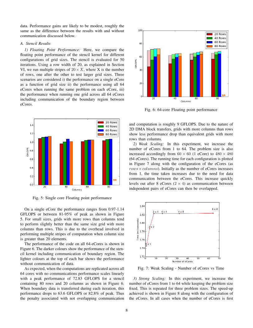
A. Stencil Results
1) Floating Point Performance: Here, we compare thefloating point performance of the stencil kernel for differentconfigurations of grid sizes. The stencil is evaluated for 50iterations. Using a row width of 20, as explained in SectionVI, we run multiple stripes of 20×X , where X is the numberof rows, one after the other to test larger grid sizes. Threescenarios are considered i) the performance on a single eCoreas a function of grid size ii) the performance using all 64eCores when running the same problem on each eCore, iii)the performance when running one grid across all 64 eCoresincluding communication of the boundary region betweeneCores.
Fig. 5: Single core Floating point performance
On a single eCore the performance ranges from 0.97-1.14GFLOPS or between 81-95% of peak as shown in Figure5. For small sizes, grids with more rows than columns tendto perform slightly better than the same size grid with morecolumns than rows. This is due to the overhead involved inperforming multiple stripes of computation when column sizeis greater than 20 elements.
The performance of the code on all 64-eCores is shown inFigure 6. The darker colours show the performance of the sten-cil kernel including communication of boundary region. Thelighter colours at the top of each bar shows the performancewithout communication of data.
As expected, when the computations are replicated across all64 cores with no communications performance scales linearlywith a peak performance of 72.83 GFLOPS for a stencilcontaining 80 rows and 20 columns as shown in Figure 6.When boundary data is transferred during each iteration, thisperformance drops to 63.6 GFLOPS or 82.8% of peak. Thusthe penalty associated with not overlapping communication
Fig. 6: 64-core Floating point performance
and computation is roughly 9 GFLOPS. Due to the nature of2D DMA block transfers, grids with more columns than rowsshow less performance drop than equivalent grids with morerows than columns.
2) Weak Scaling: In this experiment, we increase thenumber of eCores from 1 to 64. The problem size is alsoincreased accordingly from 60 × 60 (1 eCore) to 480 × 480(64 eCores). The running time for each configuration is plottedin Figure 7 along with the configuration of the eCores (asrows×columns). Initially as the number of eCores increasesfrom 1, the time taken increases due to the need for datacommunication between the eCores. This increase quicklylevels out after 8 eCores (2 × 4) as communication betweenindependent pairs of eCores can then be overlapped.
Fig. 7: Weak Scaling - Number of eCores vs Time
3) Strong Scaling: In this experiment, we increase thenumber of eCores from 1 to 64 while keeping the problem sizefixed. This is repeated for three problem sizes. The speed-upachieved is shown in Figure 8 along with the configuration ofthe eCores. In all cases when the number of eCores is first
8

doubled, a speed up of close to 2 is achieved with slightlybetter results achieved for the larger problem sizes. Furtherdoubling of the number of eCores (when possible) achievesslightly less performance gain.
Fig. 8: Strong Scaling - Number of eCores vs Speedup
VII. MATRIX MULTIPLICATION
There are several parallel algorithms for matrix multiplica-tion (matmul) on many-core systems. The approach used hereis based on Sapir [3]. Our implementation operates at threelevels:
• At the most basic level, matrix blocks that fit inside asingle eCore’s SRAM are multiplied. The requirementhere is for a matrix multiply routine that is optimized fora single eCore both in terms of performance and memoryusage.
• At the next level, if the matrices are too large to be storedon a single eCore they are block distributed across thememory of multiple eCores. The algorithm proceeds byexecuting the kernel matrix multiply on each eCore fora given set of component blocks and then shuffling theblocks between eCores, repeating this process until theoverall matrix multiplication is complete.
• At the top level, if the matrices are too large to be storedon the entire chip a procedure analogous to the blockwise algorithm outlined in the previous step is used toorchestrate movement of portions of the different matricesbetween off-chip shared memory and distributed eCorememory.
Below we expand on each of the three levels. For thepurpose of what follows we consider matrices A and B withdimensions (M × N ) and (N × K) respectively that aremultiplied together to form C with dimensions (M ×K).
Tuned single-core matmul kernel
As with the stencil code initial attempts were made todevelop the eCore matrix multiply kernel in C. This howevergave only 60 % of peak performance. Therefore the inner
most loop of the matrix multiply was replaced with hand-tunedassembly code.
The assembly code loads 4 elements of the first matrix(matrix A) into 4 registers (r11,r12,r14 and r15) at a time. Inturn each of these elements is multiplied with each element inthe corresponding row of the second matrix (matrix B) with theintermediate results accumulated into 32 registers (r32-r63).In this process the rows of matrix B are loaded 8 elementsat a time into registers r16-r23. Double-word loads are usedallowing these 8 elements to be loaded in 4 clock cycles.
By pre-loading a few elements of matrix A and B, after eachhas been used the next unprocessed element is loaded into thefreed registers. This enables load instructions and FMADDinstructions to be interleaved, although care must be takento ensure there are at least 5 cycles between using the sameregister for a load and a floating point instruction in order toavoid stalling the execution pipeline.
Each row of matrix A is loaded only once. Each element inthe row is multiplied with all the elements in the correspondingrow of matrix B. For example, the first element in a row ofmatrix A is multiplied with all the elements in the first row ofmatrix B and the intermediate results are accumulated in thefirst row of matrix C. The second element in a row of matrixA is multiplied with all the elements in the second row ofmatrix B, with the intermediate results being accumulated inthe second row of matrix C. This means that for each rowof matrix A, all the rows of matrix B need to be loadedfrom memory. Once all the elements in a row of matrixA are processed, the corresponding row of matrix C willhave its final result. These values are now written out fromthe intermediate registers to memory using double-word storeinstructions and the registers are cleared for the next row ofresults.
Assembly code structure: As with the stencil, a macro waswritten to simplify the code. The macro is used to multiply anelement of matrix A with all the elements in a row of matrixB. This involves 32 FMADD instructions and around 18 datamovement instructions interleaved, resulting in 50 instructionsexecuting 64 Flops in 32 cycles. For a 32 × 32 matmul, themacro is expanded 32 times for computing each row of productmatrix C, resulting in around 6.5 KBytes of assembly codeand 2048 Flops for each row of result. At the end of a row,the code loops around to compute another row of the resultincurring some overhead for the branch operation.
The disadvantage of writing in assembly is that the codeis not very flexible to changes to the sizes of the operandmatrices, the ’M’ dimension of matrix A being the onlyparameter which is configurable in the current code (as it is theloop count). To operate on different sizes of operand matrices,a few changes would need to be done to the assembly codeincluding the macros in order to perform matrix multiplicationefficiently for those sizes.
Memory Considerations: The operand matrices A and B,and the product matrix C are stored in the local memory ofeach eCore. Each eCore stores matrices of sizes up to 32 ×32 using a total of 12 KBytes for storing the three matrices.
9

The matrices are placed in different data banks. The operandmatrices A and B are stored in data bank 2 and the productmatrix C is stored in the last data bank (bank 3). The entirecode takes around 11 KBytes of storage and occupies the firstdata bank (bank 0) and portions of the second data bank (bank1) with the stack being allocated in the bottom half of bank 1.The size of the code has to be kept in mind while allocatingmemory for the operand matrices. This is especially importantfor the multi-core matmul version as described below.
On-chip multi-core matmul kernel
Using the single-core version as a building block, weimplement a multi-core version in order to operate on biggermatrices. With each eCore able to store operands of sizes32 × 32, we can work on matrices of size 256 × 256 withall the data residing in the local memory of the 64 eCores.
Using capitals to refer to blocks of each matrix, expandingthe matrix multiplication we obtain:
C11 = A11B11 +A12B21 +A13B31 + ...
C12 = A11B12 +A12B22 +A13B32 + ...
...
C21 = A21B11 +A22B21 +A23B31 + ...
C22 = A21B12 +A22B22 +A23B32 + ...
(1)...
If each eCore is assigned a specific block of C, we can seefrom equation 1 the blocks that are required by each eCore inorder to complete the matrix product. In the implementationused here for each matrix a row of blocks is mapped to arow of eCores. The multiplication proceeds using Cannon’salgorithm, where blocks of A are progressively rotated aroundrows of eCores while blocks of B are rotated around columnsof eCores. This process is illustrated in Figure 9.
For block sizes less than 32 × 32, double buffering isused for each of the operand matrices A and B in order tooverlap computation and communication, thereby improvingperformance. Once an eCore completes its block computation,it transfers its portion of the matrix A and B to the secondbuffers of the neighbouring eCores without waiting for theircomputation to finish.
For blocks of size 32 × 32 this is not possible. With eachmatrix requiring 4 KBytes of storage, storing the double-buffers for the operand matrices and the product matrix Cwould require a total of 20 KBytes of storage. However, sincethe size of the entire code including assembly is just over13 KBytes, this doesn’t leave enough space for the doublebuffers and the stack. Hence an alternate buffering schemewas implemented.
In this scheme the matrix A is initially allocated in eacheCore from 0x4000 to 0x4FFF and the matrix B from 0x5800to 0x67FF (4 KBytes each) and the matrix C is allocated from
Fig. 9: Assignment of blocks of A and B and data flowbetween eCores
0x7000 to 0x7FFF. A buffer of 2 KBytes is allocated adjacentto each of these matrices, from 0x5000 to 0x57FF for matrixA and 0x6800 to 0x6FFF for matrix B. Once an eCore is readyto transmit its data, it starts transferring the lower 2 KBytes ofthe matrix A onto the buffer for matrix A of the neighbouringeCore on the left side. This is followed by a transfer of thelower 2 KBytes of matrix B to the buffer for matrix B of theneighbouring eCore above it as shown in Figures 10 and 11.
Fig. 10: Transfer of Matrix A - 1st iteration
Once all the eCores complete these transfers, they starttransferring the upper halves of the matrices A and B, re-placing the lower halves of the corresponding matrices ofthe neighbours. The pointers to these two matrices are alsochanged accordingly. In the following iteration, communica-tion is performed in the reverse order as illustrated in Figures12 and 13. After changing the pointers to the two matricesagain, the allocation of the matrices would be identical to theinitial one.
Off-chip matmul kernel
For square matrices larger than 256×256 there is insufficientmemory to perform on-chip matrix multiplication, and it
10

Fig. 11: Transfer of Matrix B - 1st iteration
Fig. 12: Transfer of Matrix A - 2nd iteration
becomes necessary to page blocks of the matrices from off-chip shared memory. Here we exploit an analogous algorithmto that used to move blocks of matrices A and B betweeneCores for the on-chip case. Namely blocks of the productmatrix C are computed in turn by paging in blocks of A andB from shared memory. Thus in the 512×512 case to completeone 256× 256 block of C requires two 256× 256 blocks ofboth A and B to be read from shared memory.
A. Matrix Multiplication Results
1) Floating Point Performance: Here, we compare thefloating point performance of the matrix multiplication kernelas a function of sizes of the operand matrices.
a) Single-core Floating Point Performance: The resultsfor a single eCore are shown in Table IV. The maximum sizeof matrices that are multiplied is 32×32 as mentioned earlier.On a single eCore the performance ranges from 0.85-1.15GFLOPS or between 70-96% of peak.
b) On-chip multi-core Floating Point Performance: Ta-ble V shows the floating point performance of the on-chipmulti-core version which was implemented as detailed inSection VII. For grid sizes which are able to be fit on the
Fig. 13: Transfer of Matrix B - 2nd iteration
MatrixDimensions
GFLOPS Percentageof Peak (%)
8 × 8 0.85 70.516 × 16 1.07 89.520 × 20 1.11 92.524 × 24 1.12 93.432 × 32 1.15 95.9
TABLE IV: Matmul single core floating point performance
local memory of the chip (up to 256×256), the performance isaround 85% including the data communication between pairsof eCores. (This does not include the time taken to transferthe initial operand matrices from the external shared memoryto the chip). The table shows the per-core dimensions of theproduct matrix C and the number of eCores used to performthe multiplication. With a per-core matrix size of 32× 32, theoverall matrix dimensions would be 64× 64 when running on2 × 2 eCores, 128 × 128 on 4 × 4 eCores and 256 × 256 on8× 8 eCores.
Matrix CNum of eCores
2 × 2 4 × 4 8 × 8(per-core) GFLOPS % GFLOPS % GFLOPS %8 × 8 1.25 26.1% 5.07 26.4% 20.30 26.4%16 × 16 3.12 65.1% 12.76 66.5% 51.41 66.9%20 × 20 3.58 74.7% 14.36 74.8% 57.62 75.0%24 × 24 3.84 80.1% 15.43 80.4% 62.17 81.0%32 × 32 4.06 84.7% 16.27 84.7% 65.32 85.1%
TABLE V: Matmul multi core on-chip floating point perfor-mance
The on-chip matrix multiplication of two 256×256 matricescan be broken down into the computation of a 32× 32 matrix
11

product by each eCore and the transfer of the two operandmatrices A and B totalling 8 KBytes to the neighbouring eCorein each iteration. Considering 1.15 GFLOPS for the matrixproduct by a single eCore (from Table IV) and 2GB/s transferrate between eCores (from results in Section V), the maximumtheoretical performance can be estimated to be roughly 68GFLOPS. From Table V, the performance achieved by thecode is around 65 GFLOPS which is very close to the estimate.
c) Off-chip multi-core Floating Point Performance: Theperformance drops for sizes larger than 256× 256 due to theneed for multiple transfers of blocks to and from the sharedmemory as the algorithm progresses as discussed earlier. Theresults are shown in Table VI. A per-core matrix size of 32×32is used to perform the multiplication of large matrices of sizes512× 512 and 1024× 1024. To build the result for the largematrix size 1536×1536, a per-core size of 24×24 is used andhence the overall performance in GFLOPS is a bit worse thanthe other two cases. In all the cases, the off-chip memorytransfer dominates the overall performance with around 86-90% of the total time taken being spent on the block DMAtransfers in and out of shared memory and 10-13% of the totaltime taken being spent on the computation.
Matrix C GFLOPS % ofPeak
% Com-putation
% Shared MemTransfers
512 × 512 8.32 10.8 % 12.8 % 87.2 %1024 × 1024 8.52 11.1 % 13.1 % 86.9 %1536 × 1536 6.34 8.2 % 10.9 % 89.1 %
TABLE VI: Floating point performance for larger matrices
To analyse the performance of the off-chip matrix multi-plication, we consider the multiplication of two 512 × 512matrices. Each matrix can be considered as consisting of fourblocks of 256 × 256 elements. Each iteration in the outer-most loop in the algorithm involves transferring one block ofmatrix A and one block of matrix B from the shared memoryto the chip and having all the 64 eCores perform parallelmultiplication to produce an intermediate block result. Thetransfer of two blocks of 256 × 256 elements (512 KBytes)takes around 0.0034 seconds at 150MBytes (from results inSection V). The computation of the block matrix product takesaround 0.00051 seconds at 65.32 GFLOPS (from Table V).Thus the ratio of computation to off-chip transfers is roughly1:6.5. From the result in Table VI the ratio of computationto off-chip data transfer is 1:6.8 which is very close to theestimate.
2) Weak Scaling: In this experiment, the number of eCoresis increased from 1 to 64 while increasing the problem sizesaccordingly. Two separate configurations are tested and therunning time for each configuration is plotted in Figure 14.The problem sizes are shown as M ×N ×K. Each of theseproblems are run (wherever possible) on an eCore configura-tion of 1× 1, 2× 2, 4× 4 and 8× 8. In the first configuration,the problem size is increased from 16× 16× 32 (1 eCore) to64 × 128 × 64 (8 × 8 eCores). In the second configuration,the problem size is increased from 64 × 32 × 32 (1 eCore)
to 128× 256× 128 (8× 8 eCores). The time taken increasesinitially due to increasing data communication between theeCores. This increase quickly levels out as communicationbetween independent pairs of eCores is overlapped.
Fig. 14: Weak Scaling - Number of eCores vs Time
3) Strong Scaling: In this experiment, the number of eCoresis increased from 1 to 64 while keeping the problem sizefixed. This is repeated for four different problem sizes. Eachof these problems are run (wherever possible) on an eCoreconfiguration of 2×2, 4×4 and 8×8. The speed-up achievedis shown in Figure 15. The problem sizes are shown asM × N × K. When the number of eCores is quadrupled, aspeed up of close to 4 is achieved. Better results are achievedfor larger problem sizes as expected.
Fig. 15: Strong Scaling - Number of eCores vs Speedup
VIII. RELATED WORK AND COMPARISON WITH OTHERSYSTEMS
Similar many-core coprocessor systems include the Intel80-core terascale coprocessor [7], the 48-core single-chip
12

cloud computer (SCC) [8], [9], the 64-core Tilera Tile64SoC [10], [11], the recent Intel Xeon Phi accelerator [12]. Useof low power ARM based SoC processors [13] and many-core accelerators such as the TI C66X DSP [14], [15] forhigh performance computing are also of increasing interest. Acomparison of some of these systems is shown in Table VII.
TI C6678MulticoreDSP
Tilera64-corechip
Intel80-coreTerascaleProcessor
Epiphany64-corecoproces-sor
ChipPower(W)
10 35 97 2
Cores 8 64 80 64MaxGFLOPS
160 192 1366.4 76.8
ClockSpeed(GHz)
1.5 0.9 4.27 0.6
TABLE VII: Comparison of Epiphany with other systems
The closest related work is that of Mattson et al. [7]. Thispaper describes the challenges in programming the Intel 80-core network-on-a-chip Terascale Processor. With 80 coresrunning at 4.27 GHz, Mattson et al. ran the same five-pointstar-shaped heat diffusion stencil kernel at 1 single precisionTFLOPS while consuming 97 Watts. This is a significantcontribution as it demonstrated that high performance couldbe delivered using such many-core coprocessors. It equatesto a performance of just over 10 GFLOPS/watt. By contrastand assuming 2 watts power usage, the Epiphany system usedhere achieves roughly 32 GFLOPS/watt. (The actual powerconsumed by the chip has not been measured yet, althoughwe are currently making efforts to profile the actual powerconsumption.)
In more general work on stencil implementations, Wittmanet al. [16] explore the explicit use of shared caches inmulticore systems for implementing a pipelined temporalblocking approach for stencil computation. This techniqueperforms multiple in-cache updates on each grid point beforethe result is moved back to memory. Datta et al. [17] alsolook at improving stencil computation by examining tilingtechniques that leverage both spatial and temporal blockingof computation in order to increase data reuse. Melot et al.[18] address the performance limitation seen on many-coreprocessors due to the use of off-chip memory by implementingpipelined streaming computations. This work describes theadvantages of employing an on-chip pipelined merge sortalgorithm on the 48 core Intel SCC in an attempt to overcomethe limitation of slow off-chip memory access.
We extended the work of Sapir[3], who describes a parallelmatrix multiplication algorithm for matrices which are toolarge to be fit on the device memory. This involves blocktransfers between rows or columns of nodes using Cannon’salgorithm. The transfers are typically between nearest neigh-bours and is well suited for 2D mesh architectures such as theEpiphany. Algorithms such as SUMMA[19] and PUMMA[20]are well known distributed algorithms for matrix multiplicationinvolving block distribution of the matrices between processors
not necessarily arranged in a grid. SUMMA also has theadvantage of requiring less workspace per node enabling largerproblems to be run.
IX. CONCLUSION & FUTURE WORK
In this paper, we explored the Adapteva Epiphany 64-coreNetwork-on-chip coprocessor. Different strategies for stencilbased application codes running purely on device memorywere implemented. A tuned matrix multiplication kernel wasimplemented for multiplying matrices which fit in the devicememory along with a buffering method to overcome therelatively small memory per core. Using this a building block,an algorithm for multiplying large matrices was implemented.Micro-benchmarks were used to evaluate the performanceof several basic compute and communication operations onthe Epiphany system. The process of mapping an applicationkernel to the Epiphany architecture was demonstrated. It wasnoted that the low-level C programming primitives availablein the Epiphany SDK provided ease of use in programmingthe Epiphany. However, further work towards implementationof familiar programming models such as OpenCL [21] andthe recently launched OpenMP Accelerator model [22] forthe Epiphany is of great interest. Increasing problem sizes forstencil kernels and implementation of an efficient pipelinedkernel for large problem sizes is also of interest. We aim to ex-tend our current work by employing a pipelined algorithm forstencil computation using both spatial and temporal blockingin order to process much higher grid sizes. Such an algorithmwould ensure that computation is performed for a number ofiterations before the data is moved out of the local memoryand new data is brought in. Multiple iterations of computationcan be performed for those points for which dependent pointsare in the same block. When no more iterations are possible,another block would be streamed into the local memory toensure that computation can move forward.
In our experiments, on-chip DMA bandwidth of 2 GBytes/s,off-chip shared memory access bandwidth of 150 MBytes/sand on-chip memory latency of 11 ns for nearest neighbourwere observed. Floating point performance of roughly 64GFLOPS (82% of peak) was achieved for an optimized stencilkernel involving communication of data and a performanceof roughly 65 GFLOPS (85% of peak) was achieved for anoptimized on-chip parallel matrix multiplication. This corre-sponds to a power efficiency of roughly 32 GFLOPS/Watt onthe 64-core chip. However, extracting maximum performanceout of the system requires considerable effort on the part ofthe programmer at this stage. The relatively slow externalshared memory interface becomes a bottleneck when scalingto large problem sizes. If these are addressed, with futureversions expected to scale to 4096 cores with a peak floatingpoint performance of 5 TFLOPS and power efficiency of 70GFLOPS/Watt, the Epiphany would be a promising platformfor energy efficient high performance computing.
13
ACKNOWLEDGMENT
This work is supported in part by the Australian ResearchCouncil Discovery Project DP0987773.
REFERENCES
[1] Adapteva, “Epiphany Technical Reference Documents,” http://www.adapteva.com/all-documents.
[2] ZedBoard, “ZedBoard Development Kit,” http://www.zedboard.org/product/ zedboard.
[3] Yaniv Sapir, “Scalable Parallel Multiplication ofBig Matrices,” http://www.adapteva.com/white-papers/scalable-parallel-multiplication-of-big-matrices/ .
[4] L. E. Cannon, “A cellular computer to implement the kalman filteralgorithm.” DTIC Document, Tech. Rep., 1969.
[5] J. Dongarra, “The impact of multicore on math software andexploiting single precision computing to obtain double precisionresults,” in Parallel and Distributed Processing and Applications,ser. Lecture Notes in Computer Science, M. Guo, L. Yang,B. Di Martino, H. Zima, J. Dongarra, and F. Tang, Eds. SpringerBerlin Heidelberg, 2006, vol. 4330, pp. 2–2. [Online]. Available:http://dx.doi.org/10.1007/11946441 2
[6] A. BUTTARI, J. DONGARRA, J. K. J. LANGOU, J. L. P. LUSZCZEK,and S. TOMOV, “Exploiting mixed precision floating point hardware inscientific computations.”
[7] T. G. Mattson, R. Van der Wijngaart, and M. Frumkin, “Programmingthe intel 80-core network-on-a-chip terascale processor,” in Proceedingsof the 2008 ACM/IEEE conference on Supercomputing. IEEE Press,2008, p. 38.
[8] T. G. Mattson, M. Riepen, T. Lehnig, P. Brett, W. Haas, P. Kennedy,J. Howard, S. Vangal, N. Borkar, G. Ruhl et al., “The 48-core scc pro-cessor: the programmer’s view,” in Proceedings of the 2010 ACM/IEEEInternational Conference for High Performance Computing, Networking,Storage and Analysis. IEEE Computer Society, 2010, pp. 1–11.
[9] S. R. Vangal, J. Howard, G. Ruhl, S. Dighe, H. Wilson, J. Tschanz,D. Finan, A. Singh, T. Jacob, S. Jain et al., “An 80-tile sub-100-wteraflops processor in 65-nm cmos,” Solid-State Circuits, IEEE Journalof, vol. 43, no. 1, pp. 29–41, 2008.
[10] S. Bell, B. Edwards, J. Amann, R. Conlin, K. Joyce, V. Leung,J. MacKay, M. Reif, L. Bao, J. Brown et al., “Tile64-processor: A 64-core soc with mesh interconnect,” in Solid-State Circuits Conference,2008. ISSCC 2008. Digest of Technical Papers. IEEE International.IEEE, 2008, pp. 88–598.
[11] O. Serres, A. Anbar, S. Merchant, and T. El-Ghazawi, “Experiences withupc on tile-64 processor,” in Aerospace Conference, 2011 IEEE. IEEE,2011, pp. 1–9.
[12] A. Heinecke, K. Vaidyanathan, M. Smelyanskiy, A. Kobotov,R. Dubtsov, G. Henry, A. G. Shet, G. Chrysos, and P. Dubey, “Designand implementation of the linpack benchmark for single and multi-nodesystems based on intel R© xeon phi coprocessor,” in Parallel & Dis-tributed Processing (IPDPS), 2013 IEEE 27th International Symposiumon. IEEE, 2013, pp. 126–137.
[13] G. Mitra, B. Johnston, A. P. Rendell, E. McCreath, and J. Zhou, “Useof SIMD vector operations to accelerate application code performanceon low-powered ARM and Intel platforms,” in Parallel and DistributedProcessing Symposium Workshops & PhD Forum (IPDPSW). IEEE,2013.
[14] F. D. Igual, M. Ali, A. Friedmann, E. Stotzer, T. Wentz, and R. A. van deGeijn, “Unleashing the high-performance and low-power of multi-coredsps for general-purpose hpc,” in Proceedings of the InternationalConference on High Performance Computing, Networking, Storage andAnalysis. IEEE Computer Society Press, 2012, p. 26.
[15] E. Stotzer, A. Jayaraj, M. Ali, A. Friedmann, G. Mitra, A. P. Rendell, andI. Lintault, “Openmp on the low-power ti keystone ii arm/dsp system-on-chip,” in OpenMP in the Era of Low Power Devices and Accelerators.Springer, 2013, pp. 114–127.
[16] M. Wittmann, G. Hager, and G. Wellein, “Multicore-aware paralleltemporal blocking of stencil codes for shared and distributed mem-ory,” in Parallel & Distributed Processing, Workshops and Phd Forum(IPDPSW), 2010 IEEE International Symposium on. IEEE, 2010, pp.1–7.
[17] K. Datta, S. Kamil, S. Williams, L. Oliker, J. Shalf, and K. Yelick,“Optimization and performance modeling of stencil computations onmodern microprocessors,” SIAM review, vol. 51, no. 1, pp. 129–159,2009.
[18] N. Melot, C. Kessler, and J. Keller, “Efficient on-chip pipelined stream-ing computations on scalable manycore architectures,” 2012.
[19] R. A. Van De Geijn and J. Watts, “Summa: Scalable universal matrixmultiplication algorithm,” Concurrency-Practice and Experience, vol. 9,no. 4, pp. 255–274, 1997.
[20] J. Choi, D. W. Walker, and J. J. Dongarra, “Pumma: Parallel universalmatrix multiplication algorithms on distributed memory concurrentcomputers,” Concurrency: Practice and Experience, vol. 6, no. 7, pp.543–570, 1994.
[21] J. E. Stone, D. Gohara, and G. Shi, “OpenCL: A ParallelProgramming Standard for Heterogeneous Computing Systems,” IEEEDes. Test, vol. 12, no. 3, pp. 66–73, May 2010. [Online]. Available:http://dx.doi.org/10.1109/MCSE.2010.69
[22] J. C. Beyer, E. J. Stotzer, A. Hart, and B. R. de Supinski, “OpenMPfor accelerators,” in OpenMP in the Petascale Era. Springer, 2011, pp.108–121.
14


![Epiphany [2015]](https://img.pdfslide.net/doc/110x75/568ca9641a28ab186d9d48fd/epiphany-2015.jpg)