Embed Size (px)
Citation preview
Epiphany-V: A 1024 processor 64-bit RISC System-On-Chip
Epiphany-V: A 1024 processor 64-bit RISC System-On-Chip
By Andreas OlofssonAdapteva Inc, Lexington, MA, [email protected]
Abstract
This paper describes the design of a 1024-core processor chip in 16nm FinFet technology. The chip(“Epiphany-V”) contains an array of 1024 64-bit RISC processors, 64MB of on-chip SRAM, three 136-bitwide mesh Networks-On-Chip, and 1024 programmable IO pins. The chip has taped out and is beingmanufactured by TSMC.
This research was developed with funding from the Defense Advanced Research Projects Agency (DARPA).The views, opinions and/or findings expressed are those of the author and should not be interpreted asrepresenting the official views or policies of the Department of Defense or the U.S. Government.
Keywords: RISC, Network-on-Chip (NoC), HPC, parallel, many-core, 16nm FinFET
I. Introduction
Applications like deep learning, self-driving cars, autonomous drones, and cognitive radio need an order ofmagnitude boost in processing efficiency to unlock their true potentials. The primary goal for this projectis to build a parallel processor with 1024 RISC cores demonstrating a processing energy efficiency of 75GFLOPS/Watt. A secondary goal for this project is to demonstrate a 100x reduction in chip design costsfor advanced node ASICs. Significant energy savings of 10-100x can be achieved through extreme siliconcustomization, but customization is not financially viable if chip design costs are prohibitive. The generalconsensus is that it costs anywhere from $20M to $1B to design a leading edge System-On-Chip platform.[1-4]
II. History
The System-On-Chip described in this paper is the 5th generation of the Epiphany parallel processor archi-tecture invented by Andreas Olofsson in 2008.[5] The Epiphany architecture was created to address energyefficiency and peak performance limitations in real time communication and image processing applications.
The first Epiphany product was a 16-core 65nm System-On-Chip (“Epiphany-III”) released in May 2011.The chip worked beyond expectations and is still being produced today.[6]
The second Epiphany product was a 28nm 64-core SOC (“Epiphany-IV”) completed in the summer of2011.[7] The Epiphany-IV chips demonstrated 70 GFLOPS/Watt processing efficiency at the core supplylevel and was the most energy-efficient processor available at that time. The chip was sampled to a numberof customers and partners, but was not produced in volume due to lack of funding. At that time, Adaptevaalso created a physical implementation of a 1024 core 32-bit RISC processor array, but it was never tapedout due to funding constraints.
In 2012 Adapteva launched an open source $99 Epiphany-III based single board computer on Kickstartercalled Parallella.[8] The goal of the project was to democratize access to parallel computing for researchersand programming enthusiasts. The project was highly successful and raised close to $1M on Kickstarter.To date the Parallella computer has shipped to over 10,000 customers and has generated over 100 technicalpublications.[9]
For a complete description of the Epiphany processor history and design decisions, please refer to the paper“Kickstarting high-performance energy-efficient manycore architectures with Epiphany”.[10]
1
Epiphany-V: A 1024 processor 64-bit RISC System-On-Chip
III. Architecture
III.A Overview
The Epiphany architecture is a distributed shared memory architecture comprised of an array of RISCprocessors communicating via a low-latency mesh Network-on-Chip. Each node in the processor array is acomplete RISC processor capable of running an operating system (“MIMD”). Epiphany uses a flat cache-lessmemory model, in which all distributed memory is readable and writable by all processors in the system.
The Epiphany-V introduces a number of new capabilities compared to previous Epiphany products, including64-bit memory addressing, 64-bit floating point operations, 2X the memory per processor, and custom ISAsfor deep learning, communication, and cryptography. The following figure shows a high level diagram of theEpiphany-V implementation.
Figure 1: Epiphany-V Overview
Summary of Epiphany-V features:
• 1024 64-bit RISC processors• 64-bit memory architecture• 64/32-bit IEEE floating point support• 64MB of distributed on-chip memory• 1024 programmable I/O signals• Three 136-bit wide 2D mesh NOCs• 2052 Independent Power Domains• Support for up to 1 billion shared memory processors• Binary compatibility with Epiphany III/IV chips• Custom ISA extensions for deep learning, communication, and cryptography
As in previous Epiphany versions, multiple chips can be connected together at the board and system levelusing point to point links. Epiphany-V has 128 point-to-point I/O links for chip to chip communication.
2
Epiphany-V: A 1024 processor 64-bit RISC System-On-Chip
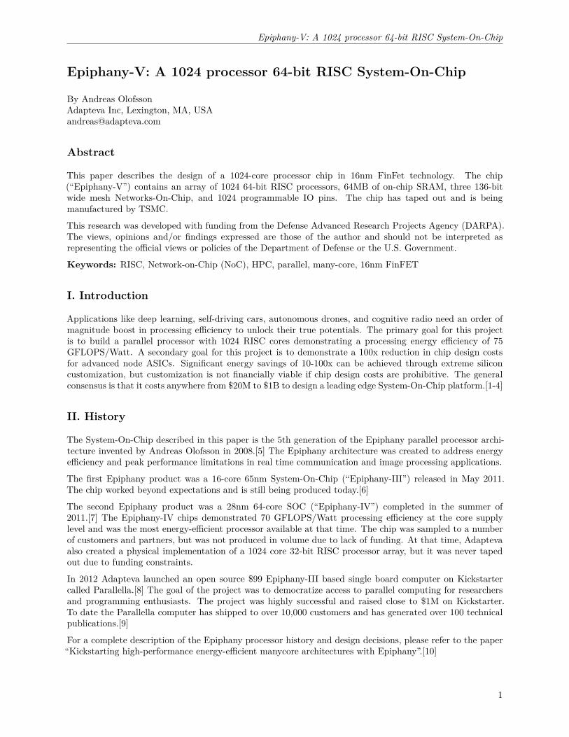
In aggregate, the Epiphany 64-bit architecture supports systems with up to 1 Billion cores and 1 Petabyte(10ˆ15) of total memory.
Figure 2: Multichip configuration
The following sections describe the Epiphany architecture. For complete details, please refer to the onlinearchitecture reference manual.[11]
III.B Memory Architecture
The Epiphany 64-bit memory map is split into 1 Billion 1MB memory regions, with 30 bits dedicated tox,y,z addressing. The complete Epiphany memory map is flat, distributed, and shared by all processors inthe system. Each individual memory region can be used by a single processor or aggregated as part of ashared memory pool. The Epiphany architecture uses multi-banked software-managed scratch-pad memoryat each processor node. On every clock cycle, a processor node can:
• Fetch 8 bytes of instructions• Load/store 8 bytes of data• Receive 8 bytes from another processor in the system• Send 8 bytes to another processor in the system
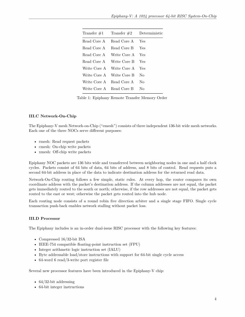
The Epiphany architecture uses strong memory ordering for local load/stores and weak memory orderingremote transfers.
3
Epiphany-V: A 1024 processor 64-bit RISC System-On-Chip
Transfer #1 Transfer #2 Deterministic
Read Core A Read Core A YesRead Core A Read Core B YesRead Core A Write Core A YesRead Core A Write Core B YesWrite Core A Write Core A YesWrite Core A Write Core B NoWrite Core A Read Core A NoWrite Core A Read Core B No
Table 1: Epiphany Remote Transfer Memory Order
III.C Network-On-Chip
The Epiphany-V mesh Network-on-Chip (“emesh”) consists of three independent 136-bit wide mesh networks.Each one of the three NOCs serve different purposes:
• rmesh: Read request packets• cmesh: On-chip write packets• xmesh: Off-chip write packets
Epiphany NOC packets are 136 bits wide and transferred between neighboring nodes in one and a half clockcycles. Packets consist of 64 bits of data, 64 bits of address, and 8 bits of control. Read requests puts asecond 64-bit address in place of the data to indicate destination address for the returned read data.
Network-On-Chip routing follows a few simple, static rules. At every hop, the router compares its owncoordinate address with the packet’s destination address. If the column addresses are not equal, the packetgets immediately routed to the south or north; otherwise, if the row addresses are not equal, the packet getsrouted to the east or west; otherwise the packet gets routed into the hub node.
Each routing node consists of a round robin five direction arbiter and a single stage FIFO. Single cycletransaction push-back enables network stalling without packet loss.
III.D Processor
The Epiphany includes is an in-order dual-issue RISC processor with the following key features:
• Compressed 16/32-bit ISA• IEEE-754 compatible floating-point instruction set (FPU)• Integer arithmetic logic instruction set (IALU)• Byte addressable load/store instructions with support for 64-bit single cycle access• 64-word 6 read/3-write port register file
Several new processor features have been introduced in the Epiphany-V chip:
• 64/32-bit addressing• 64-bit integer instructions
4
Epiphany-V: A 1024 processor 64-bit RISC System-On-Chip
• 64-bit IEEE floating point support• SIMD 32-bit IEEE floating point support• Expanded shared memory support for up to 1 Billion cores• Custom ISA extensions for deep learning, communication, and cryptography
III.E I/O
The Epiphany-V has a total of 1024 programmable I/O pins and 16 control input pins. The programmableI/O is configured through 32 independent IO modules “io-slices” on each side of the chip (north, east, west,south). All io-slices can be independently configured as fast point-to-point links or as GPIO pins.
When the IO modules are configured as links, epiphany memory transactions are transferred across the IOlinks automatically, effectively extending the on-chip 2D mesh network to other chips. The glueless memorytransfer point-to-point I/O links combined with 64-bit addressability enables construction of shared memorysystems with up to 1 Billion Epiphany processors.
IV. Performance
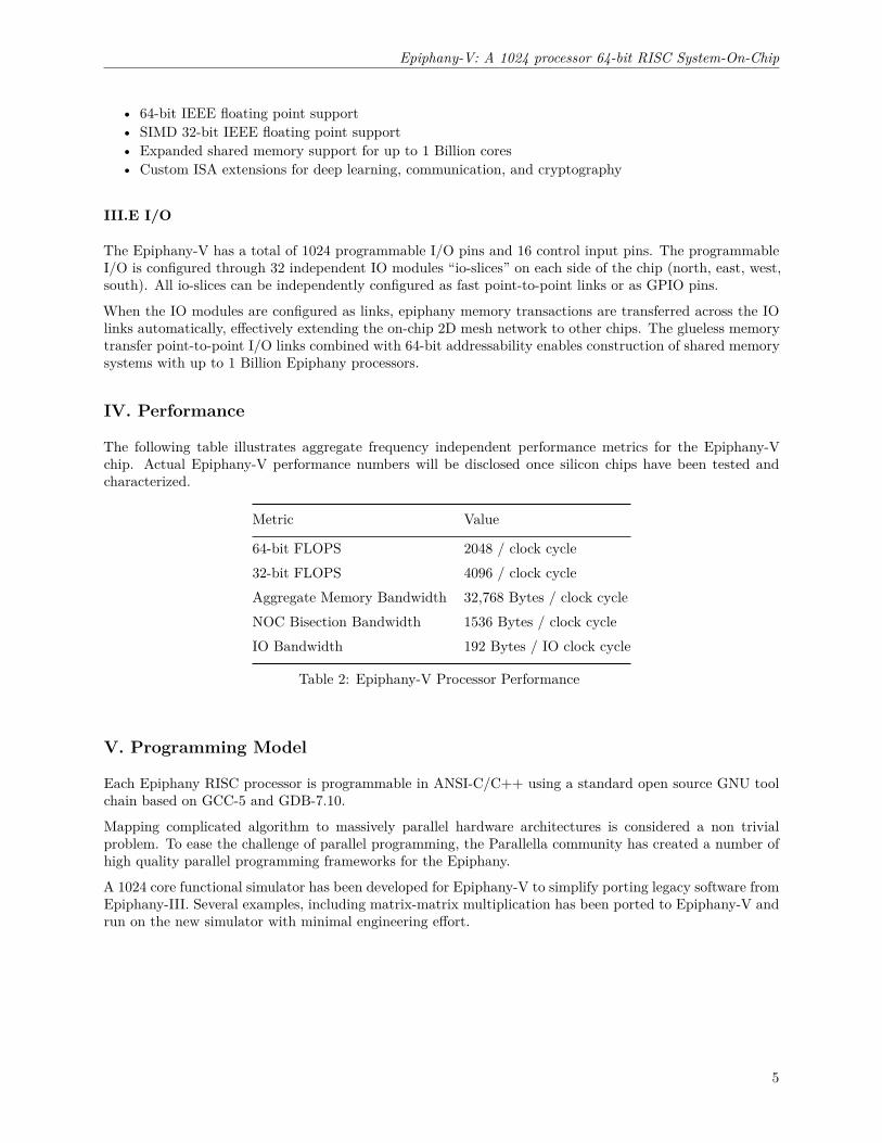
The following table illustrates aggregate frequency independent performance metrics for the Epiphany-Vchip. Actual Epiphany-V performance numbers will be disclosed once silicon chips have been tested andcharacterized.
Metric Value
64-bit FLOPS 2048 / clock cycle32-bit FLOPS 4096 / clock cycleAggregate Memory Bandwidth 32,768 Bytes / clock cycleNOC Bisection Bandwidth 1536 Bytes / clock cycleIO Bandwidth 192 Bytes / IO clock cycle
Table 2: Epiphany-V Processor Performance
V. Programming Model
Each Epiphany RISC processor is programmable in ANSI-C/C++ using a standard open source GNU toolchain based on GCC-5 and GDB-7.10.
Mapping complicated algorithm to massively parallel hardware architectures is considered a non trivialproblem. To ease the challenge of parallel programming, the Parallella community has created a number ofhigh quality parallel programming frameworks for the Epiphany.
A 1024 core functional simulator has been developed for Epiphany-V to simplify porting legacy software fromEpiphany-III. Several examples, including matrix-matrix multiplication has been ported to Epiphany-V andrun on the new simulator with minimal engineering effort.
5
Epiphany-V: A 1024 processor 64-bit RISC System-On-Chip
Framework Author Reference
OpenMP University of Ioannina [12]MPI BDT/ARL [13]OpenSHMEM ARL [14]OpenCL BDT [15]Erlang Uppsala University [16]Bulk Synchronous Parallel (BSP) Coduin [17]Epython Nick Brown [18]PAL Adapteva/community [19]
Table 3: Supported Epiphany Programming Frameworks
VI. Chip Implementation
VI.A Physical Design Details
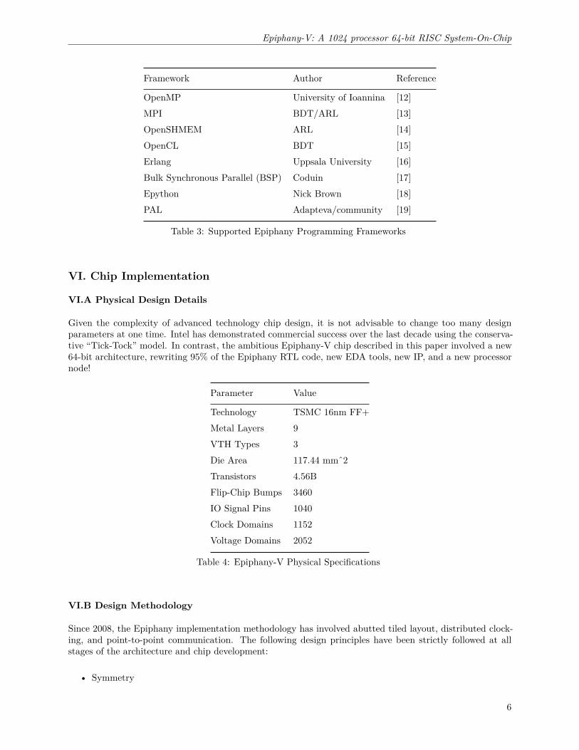
Given the complexity of advanced technology chip design, it is not advisable to change too many designparameters at one time. Intel has demonstrated commercial success over the last decade using the conserva-tive “Tick-Tock” model. In contrast, the ambitious Epiphany-V chip described in this paper involved a new64-bit architecture, rewriting 95% of the Epiphany RTL code, new EDA tools, new IP, and a new processornode!
Parameter Value
Technology TSMC 16nm FF+Metal Layers 9VTH Types 3Die Area 117.44 mmˆ2Transistors 4.56BFlip-Chip Bumps 3460IO Signal Pins 1040Clock Domains 1152Voltage Domains 2052
Table 4: Epiphany-V Physical Specifications
VI.B Design Methodology
Since 2008, the Epiphany implementation methodology has involved abutted tiled layout, distributed clock-ing, and point-to-point communication. The following design principles have been strictly followed at allstages of the architecture and chip development:
• Symmetry
6
Epiphany-V: A 1024 processor 64-bit RISC System-On-Chip
• Modularity• Scalability• Simplicity
The Epiphany-V required significant advances to accommodate large array size and advanced process tech-nology node. Novel circuit topologies were created to solve critical issues in the areas of clocking, reset,power grids, synchronization, fault tolerance, and standby power.
VI.C Chip Layout
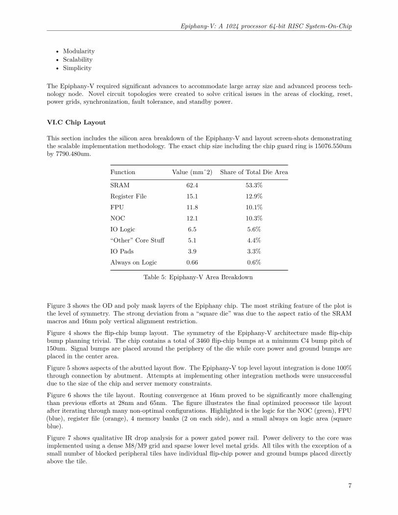
This section includes the silicon area breakdown of the Epiphany-V and layout screen-shots demonstratingthe scalable implementation methodology. The exact chip size including the chip guard ring is 15076.550umby 7790.480um.
Function Value (mmˆ2) Share of Total Die Area
SRAM 62.4 53.3%Register File 15.1 12.9%FPU 11.8 10.1%NOC 12.1 10.3%IO Logic 6.5 5.6%“Other” Core Stuff 5.1 4.4%IO Pads 3.9 3.3%Always on Logic 0.66 0.6%
Table 5: Epiphany-V Area Breakdown
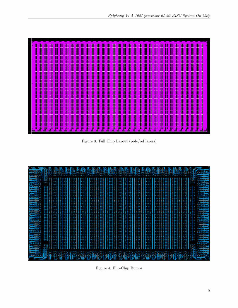
Figure 3 shows the OD and poly mask layers of the Epiphany chip. The most striking feature of the plot isthe level of symmetry. The strong deviation from a “square die” was due to the aspect ratio of the SRAMmacros and 16nm poly vertical alignment restriction.
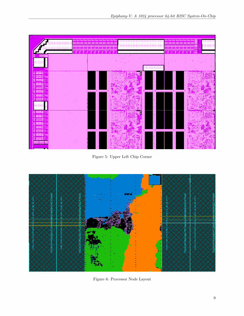
Figure 4 shows the flip-chip bump layout. The symmetry of the Epiphany-V architecture made flip-chipbump planning trivial. The chip contains a total of 3460 flip-chip bumps at a minimum C4 bump pitch of150um. Signal bumps are placed around the periphery of the die while core power and ground bumps areplaced in the center area.
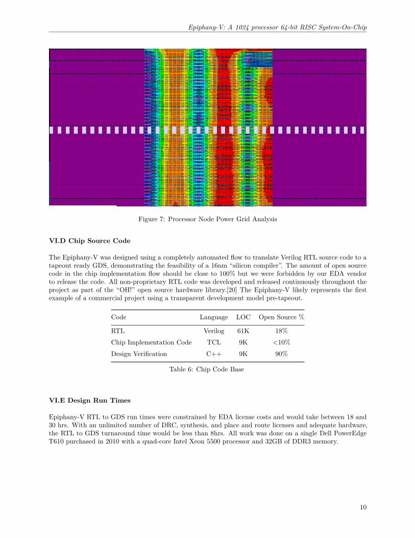
Figure 5 shows aspects of the abutted layout flow. The Epiphany-V top level layout integration is done 100%through connection by abutment. Attempts at implementing other integration methods were unsuccessfuldue to the size of the chip and server memory constraints.
Figure 6 shows the tile layout. Routing convergence at 16nm proved to be significantly more challengingthan previous efforts at 28nm and 65nm. The figure illustrates the final optimized processor tile layoutafter iterating through many non-optimal configurations. Highlighted is the logic for the NOC (green), FPU(blue), register file (orange), 4 memory banks (2 on each side), and a small always on logic area (squareblue).
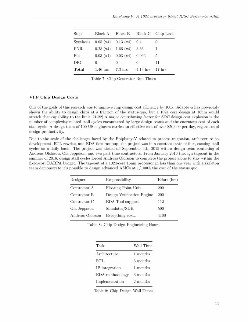
Figure 7 shows qualitative IR drop analysis for a power gated power rail. Power delivery to the core wasimplemented using a dense M8/M9 grid and sparse lower level metal grids. All tiles with the exception of asmall number of blocked peripheral tiles have individual flip-chip power and ground bumps placed directlyabove the tile.
7
Epiphany-V: A 1024 processor 64-bit RISC System-On-Chip
Figure 3: Full Chip Layout (poly/od layers)
Figure 4: Flip-Chip Bumps
8
Epiphany-V: A 1024 processor 64-bit RISC System-On-Chip
Figure 5: Upper Left Chip Corner
Figure 6: Processor Node Layout
9
Epiphany-V: A 1024 processor 64-bit RISC System-On-Chip
Figure 7: Processor Node Power Grid Analysis
VI.D Chip Source Code
The Epiphany-V was designed using a completely automated flow to translate Verilog RTL source code to atapeout ready GDS, demonstrating the feasibility of a 16nm “silicon compiler”. The amount of open sourcecode in the chip implementation flow should be close to 100% but we were forbidden by our EDA vendorto release the code. All non-proprietary RTL code was developed and released continuously throughout theproject as part of the “OH!” open source hardware library.[20] The Epiphany-V likely represents the firstexample of a commercial project using a transparent development model pre-tapeout.
Code Language LOC Open Source %
RTL Verilog 61K 18%Chip Implementation Code TCL 9K <10%Design Verification C++ 9K 90%
Table 6: Chip Code Base
VI.E Design Run Times
Epiphany-V RTL to GDS run times were constrained by EDA license costs and would take between 18 and30 hrs. With an unlimited number of DRC, synthesis, and place and route licenses and adequate hardware,the RTL to GDS turnaround time would be less than 8hrs. All work was done on a single Dell PowerEdgeT610 purchased in 2010 with a quad-core Intel Xeon 5500 processor and 32GB of DDR3 memory.
10
Epiphany-V: A 1024 processor 64-bit RISC System-On-Chip
Step Block A Block B Block C Chip Level
Synthesis 0.05 (x4) 0.13 (x4) 0.4 0PNR 0.28 (x4) 1.66 (x4) 3.66 1Fill 0.03 (x4) 0.03 (x4) 0.066 5DRC 0 0 0 11Total 1.46 hrs 7.3 hrs 4.13 hrs 17 hrs
Table 7: Chip Generator Run Times
VI.F Chip Design Costs
One of the goals of this research was to improve chip design cost efficiency by 100x. Adapteva has previouslyshown the ability to design chips at a fraction of the status-quo, but a 1024 core design at 16nm wouldstretch that capability to the limit.[21-22] A major contributing factor for SOC design cost explosion is thenumber of complexity related stall cycles encountered by large design teams and the enormous cost of eachstall cycle. A design team of 100 US engineers carries an effective cost of over $50,000 per day, regardless ofdesign productivity.
Due to the scale of the challenges faced by the Epiphany-V related to process migration, architecture co-development, RTL rewrite, and EDA flow rampup, the project was in a constant state of flux, causing stallcycles on a daily basis. The project was kicked off September 9th, 2015 with a design team consisting ofAndreas Olofsson, Ola Jeppsson, and two part time contractors. From January 2016 through tapeout in thesummer of 2016, design stall cycles forced Andreas Olofsson to complete the project alone to stay within thefixed-cost DARPA budget. The tapeout of a 1024-core 16nm processor in less than one year with a skeletonteam demonstrate it’s possible to design advanced ASICs at 1/100th the cost of the status quo.
Designer Responsibility Effort (hrs)
Contractor A Floating Point Unit 200Contractor B Design Verification Engine 200Contractor C EDA Tool support 112Ola Jeppsson Simulator/SDK 500Andreas Olofsson Everything else… 4100
Table 8: Chip Design Engineering Hours
Task Wall Time
Architecture 1 monthsRTL 3 monthsIP integration 1 monthsEDA methodology 3 monthsImplementation 2 months
Table 9: Chip Design Wall Times
11
Epiphany-V: A 1024 processor 64-bit RISC System-On-Chip
Epiphany-V World Record/First Mark
Chip with largest # of General Purpose Processors 1024Highest Density HPC Chip 38M transistors/mmˆ2Most efficient chip design team 900K transistors/hourMost efficient RTL to GDS Chip Design flow 150M transistors/hourLargest chip designed by one full time designer 4.5B
Table 10: Epiphany-V Design Efficiency Benchmarks
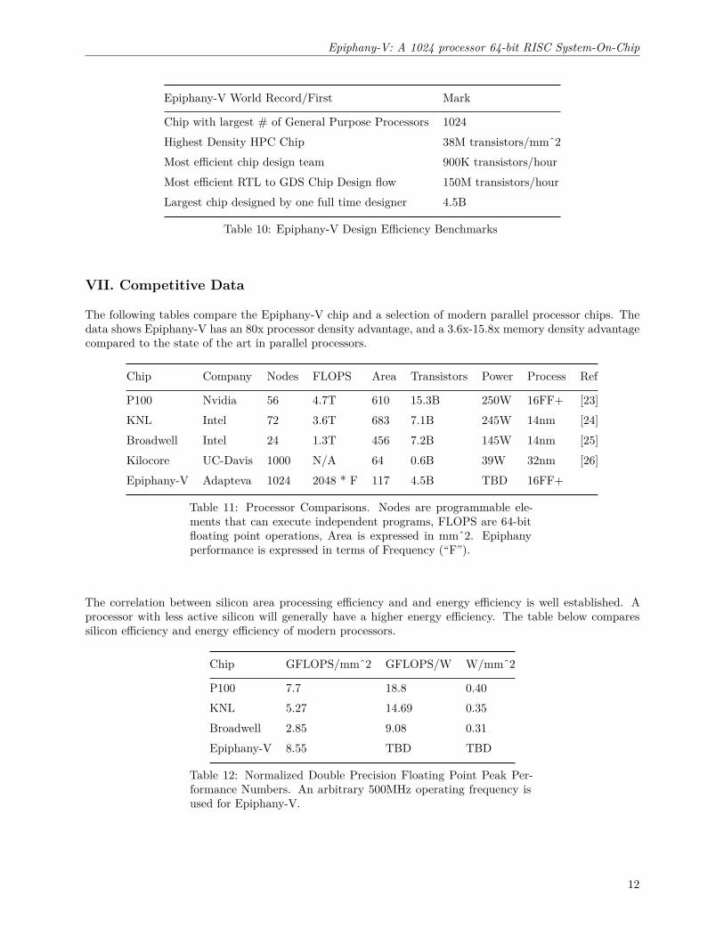
VII. Competitive Data
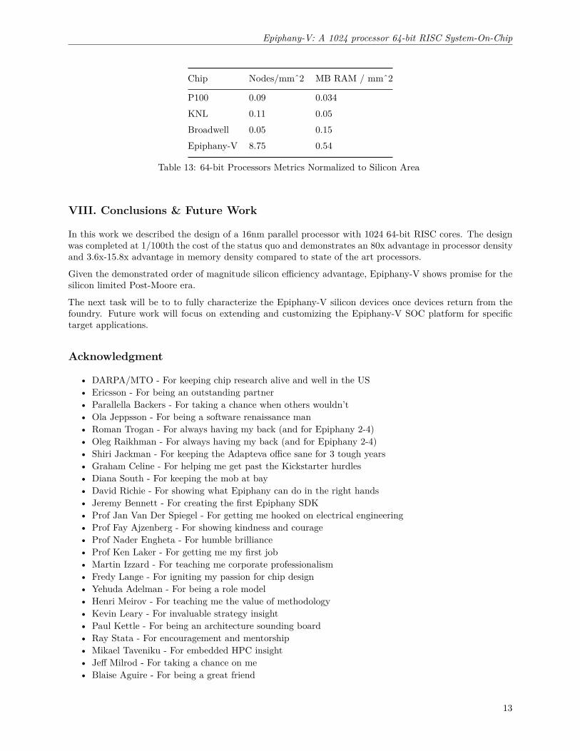
The following tables compare the Epiphany-V chip and a selection of modern parallel processor chips. Thedata shows Epiphany-V has an 80x processor density advantage, and a 3.6x-15.8x memory density advantagecompared to the state of the art in parallel processors.
Chip Company Nodes FLOPS Area Transistors Power Process Ref
P100 Nvidia 56 4.7T 610 15.3B 250W 16FF+ [23]KNL Intel 72 3.6T 683 7.1B 245W 14nm [24]Broadwell Intel 24 1.3T 456 7.2B 145W 14nm [25]Kilocore UC-Davis 1000 N/A 64 0.6B 39W 32nm [26]Epiphany-V Adapteva 1024 2048 * F 117 4.5B TBD 16FF+
Table 11: Processor Comparisons. Nodes are programmable ele-ments that can execute independent programs, FLOPS are 64-bitfloating point operations, Area is expressed in mmˆ2. Epiphanyperformance is expressed in terms of Frequency (“F”).
The correlation between silicon area processing efficiency and and energy efficiency is well established. Aprocessor with less active silicon will generally have a higher energy efficiency. The table below comparessilicon efficiency and energy efficiency of modern processors.
Chip GFLOPS/mmˆ2 GFLOPS/W W/mmˆ2
P100 7.7 18.8 0.40KNL 5.27 14.69 0.35Broadwell 2.85 9.08 0.31Epiphany-V 8.55 TBD TBD
Table 12: Normalized Double Precision Floating Point Peak Per-formance Numbers. An arbitrary 500MHz operating frequency isused for Epiphany-V.
12
Epiphany-V: A 1024 processor 64-bit RISC System-On-Chip
Chip Nodes/mmˆ2 MB RAM / mmˆ2
P100 0.09 0.034KNL 0.11 0.05Broadwell 0.05 0.15Epiphany-V 8.75 0.54
Table 13: 64-bit Processors Metrics Normalized to Silicon Area
VIII. Conclusions & Future Work
In this work we described the design of a 16nm parallel processor with 1024 64-bit RISC cores. The designwas completed at 1/100th the cost of the status quo and demonstrates an 80x advantage in processor densityand 3.6x-15.8x advantage in memory density compared to state of the art processors.
Given the demonstrated order of magnitude silicon efficiency advantage, Epiphany-V shows promise for thesilicon limited Post-Moore era.
The next task will be to to fully characterize the Epiphany-V silicon devices once devices return from thefoundry. Future work will focus on extending and customizing the Epiphany-V SOC platform for specifictarget applications.
Acknowledgment
• DARPA/MTO - For keeping chip research alive and well in the US• Ericsson - For being an outstanding partner• Parallella Backers - For taking a chance when others wouldn’t• Ola Jeppsson - For being a software renaissance man• Roman Trogan - For always having my back (and for Epiphany 2-4)• Oleg Raikhman - For always having my back (and for Epiphany 2-4)• Shiri Jackman - For keeping the Adapteva office sane for 3 tough years• Graham Celine - For helping me get past the Kickstarter hurdles• Diana South - For keeping the mob at bay• David Richie - For showing what Epiphany can do in the right hands• Jeremy Bennett - For creating the first Epiphany SDK• Prof Jan Van Der Spiegel - For getting me hooked on electrical engineering• Prof Fay Ajzenberg - For showing kindness and courage• Prof Nader Engheta - For humble brilliance• Prof Ken Laker - For getting me my first job• Martin Izzard - For teaching me corporate professionalism• Fredy Lange - For igniting my passion for chip design• Yehuda Adelman - For being a role model• Henri Meirov - For teaching me the value of methodology• Kevin Leary - For invaluable strategy insight• Paul Kettle - For being an architecture sounding board• Ray Stata - For encouragement and mentorship• Mikael Taveniku - For embedded HPC insight• Jeff Milrod - For taking a chance on me• Blaise Aguire - For being a great friend
13
Epiphany-V: A 1024 processor 64-bit RISC System-On-Chip
• Ulla Olofsson (Mamma) - For always being there• Rolf Olofsson (Pappa) - For teaching me to always follow my passion• Sharon Olofsson - For everything
References
• [1] Cadence Blog, Are SoC Development Costs Significantly Underestimated?
• [2] Ed Sperling, How Much Will That Chip Cost?, Semi Engineering, March 27, 2014
• [3] Rick Merritt, Nvidia calls for move to 450mm wafers, EE Times, April 2012
• [4] Ron Wilson, Designers report on multi-million gate ASICs, EE Times, June 2002
• [5] A. Olofsson, Mesh network, U.S. Patent 8,531,943, Filed October 29 2009, Issued September 10,2013,
• [6] A. Olofsson, R. Trogan, and O. Raikhman, A 1024-core 70 GFLOP/W Floating Point ManycoreMicroprocessor, 15th Annual Workshop on High Performance Embedded Computing, Sept 2011
• [7] Adapteva, E16G301 Datasheet
• [8] Adapteva, Parallella Kickstarter Project
• [9] Parallella Publication List, https://parallella.org/publications
• [10] A. Olofsson, T. Nordström and Z. Ul-Abdin, Kickstarting High-performance Energy-efficient Many-core Architectures with Epiphany 2014 48th Asilomar Conference on Signals, Systems and Computers,Pacific Grove, CA, 2014, pp. 1719-1726
• [11] A. Olofsson, Epiphany Architecture Reference Manual
• [12] Alexandros Papadogiannakis, Spiros N. Agathos, Vassilios V. Dimakopoulo, OpenMP 4.0 DeviceSupport in the OMPi Compiler, OpenMP: Heterogenous Execution and Data Movements, Volume 9342of the series Lecture Notes in Computer Science pp 202-216
• [13] James Ross, David Richie, Song Park, Dale Shires, Parallel programming model for the Epiphanymany-core co-processor using threaded MPI, Microprocessors and Microsystems, Volume 43, Pages95-103, June 2016
• [14] James Ross,David Richie, An OpenSHMEM Implementation for the Adapteva Epiphany Copro-cessor, OpenSHMEM 2016, Third workshop on OpenSHMEM and Related Technologies
• [15] David Richie, James Ross, OpenCL + OpenSHMEM Hybrid Programming Model for the AdaptevaEpiphany Architecture, OpenSHMEM 2016, Third workshop on OpenSHMEM and Related Technolo-gies
• [16] Magnus Lang, Kostis Sagonas, Running Erlang on the Parallella, Erlang User Conference 2015
• [17] Jan-Willem Buurlage, Tom Bannink, Abe Wits, Bulk-synchronous pseudo-streaming algorithmsfor many-core accelerators, HLPP 2016: International Symposia on High-Level Parallel Programmingand Applications
• [18] Nick Brown, Epython Library, https://github.com/mesham/epython
• [19] Andreas Olofsson, et al, PAL Library, https://github.com/parallella/pal
• [20] Andreas Olofsson, et al, OH! Library, https://github.com/parallella/oh
• [21] Andreas Olofsson, A Lean Fabless Semiconductor Business Model, 2012 GSA Global
14
Epiphany-V: A 1024 processor 64-bit RISC System-On-Chip
• [22] Clive Maxfield, From RTL to GDSII in Just Six Weeks, EETimes Nov 2011
• [23] NVIDIA, Inside Pascal
• [24] Ian Cutress, SuperComputing 15: Intel’s Knights Landing Xeon Phi Silicon on Display, November19, 2015
• [25] Johan De Gelas, The Intel Xeon E5 v4 Review: Testing Broadwell-EP With Demanding ServerWorkloads, Anandtech, June 13 2016
• [26] Brent Bohnenstiehl, Aaron Stillmaker, Jon Pimentel, Timothy Andreas, Bin Liu, Anh Tran, Em-manuel Adeagbo and Bevan Baas, KiloCore: A 32 nm 1000-Processor Array, IEEE HotChips Sympo-sium on High-Perfomance Chips, August 2016
15