Embed Size (px)
Citation preview

PVT Compensated OTA Design
on SOI-CMOS Nanometer
Technologies
By
Francisco Javier Villota Salazar
Electronics Engineer, Universidad Industrial de Santander.
A Dissertation submitted in partial fulfillment of the
requirements for the degree of:
MASTER OF SCIENCE WITHMAJOR ON
ELECTRONICS
at the
Instituto Nacional de Astrofısica Optica y Electronica
August 2012
Tonantzintla, Puebla
Advisor:
Ph.D. Guillermo Espinosa Flores-Verdad
Principal Research Scientist
Electronics Department
INAOE
c©INAOE 2012
The author hereby grants to INAOE permission to
reproduce and to distribute copies of this Thesis document
in whole or in part.


.
“To my parents Mario and Nubia Consuelo,
to my sister Andrea and my dear Marıa”
“A mis padres Mario y Nubia Consuelo,
mi hermana Andrea y mi querida Marıa”
Francisco.

Contents
Acknowledgments . . . . . . . . . . . . . . . . . . . . . . . . . . . . . . . . . vi
Agradecimientos . . . . . . . . . . . . . . . . . . . . . . . . . . . . . . . . . . vii
Summary . . . . . . . . . . . . . . . . . . . . . . . . . . . . . . . . . . . . . . viii
Resumen . . . . . . . . . . . . . . . . . . . . . . . . . . . . . . . . . . . . . . . ix
List of Figures . . . . . . . . . . . . . . . . . . . . . . . . . . . . . . . . . . . xii
List of Tables . . . . . . . . . . . . . . . . . . . . . . . . . . . . . . . . . . . . xiii
Acronyms . . . . . . . . . . . . . . . . . . . . . . . . . . . . . . . . . . . . . . xiv
1 Analog in Nanometers 1
1.1 Introduction . . . . . . . . . . . . . . . . . . . . . . . . . . . . . . . . . . . 1
1.2 Short Channel Effects, Scaling and Technology . . . . . . . . . . . . . . . . 3
1.2.1 Non-viability of scaling in CMOS to analog design . . . . . . . . . . 3
1.2.2 Silicon on insulator technology . . . . . . . . . . . . . . . . . . . . . 4
1.2.2.1 Partially depleted vs. Fully depleted . . . . . . . . . . . . 7
1.3 IBM 45 nm Partially Depleted SOI Technology . . . . . . . . . . . . . . . 8
1.3.1 Overview . . . . . . . . . . . . . . . . . . . . . . . . . . . . . . . . 8
1.3.2 Transistor selection . . . . . . . . . . . . . . . . . . . . . . . . . . . 9
1.3.3 Behavior of selected transistors . . . . . . . . . . . . . . . . . . . . 10
1.4 Restrictions and Drawbacks in Amplifier Design . . . . . . . . . . . . . . . 13
1.5 PVT Specifications and Simulation . . . . . . . . . . . . . . . . . . . . . . 14
1.5.1 Additional effects covered by simulation . . . . . . . . . . . . . . . 16
1.6 Rail-to-Rail OTA Design Perspective . . . . . . . . . . . . . . . . . . . . . 16
2 Sub-threshold Operation and Current Switching for Input Stage 19
2.1 Improving Transistor Behavior . . . . . . . . . . . . . . . . . . . . . . . . . 19
2.1.1 Compound transistor . . . . . . . . . . . . . . . . . . . . . . . . . . 20
2.1.2 Transistors Matrix . . . . . . . . . . . . . . . . . . . . . . . . . . . 21
2.1.3 Limits and justification . . . . . . . . . . . . . . . . . . . . . . . . . 23

CONTENTS v
2.2 Conventional topologies . . . . . . . . . . . . . . . . . . . . . . . . . . . . 23
2.2.1 Dynamic compensation . . . . . . . . . . . . . . . . . . . . . . . . . 26
2.2.2 PVT Analysis . . . . . . . . . . . . . . . . . . . . . . . . . . . . . . 28
2.3 Feedback Differential Pair . . . . . . . . . . . . . . . . . . . . . . . . . . . 30
2.3.1 Rail-to-rail input stage with FDP . . . . . . . . . . . . . . . . . . . 32
2.4 Improved and Compensated FDP-R2R Stage . . . . . . . . . . . . . . . . . 35
2.4.1 Results and comparison with other works . . . . . . . . . . . . . . . 38
3 Double gm Addition and Proper Biasing for Gain Stage 41
3.1 Disadvantages For High Gain . . . . . . . . . . . . . . . . . . . . . . . . . 41
3.1.1 Flat-Band gain’s variation . . . . . . . . . . . . . . . . . . . . . . . 42
3.1.1.1 Possible causes and an effective solution . . . . . . . . . . 45
3.2 Robust Design . . . . . . . . . . . . . . . . . . . . . . . . . . . . . . . . . . 46
3.2.1 Structures for high gain . . . . . . . . . . . . . . . . . . . . . . . . 49
3.3 One stage proposed architecture . . . . . . . . . . . . . . . . . . . . . . . . 52
3.3.1 Common mode feedback circuit . . . . . . . . . . . . . . . . . . . . 54
3.3.2 Simulation . . . . . . . . . . . . . . . . . . . . . . . . . . . . . . . . 56
3.4 Proposed architecture for two stages . . . . . . . . . . . . . . . . . . . . . 59
3.4.1 Compensation . . . . . . . . . . . . . . . . . . . . . . . . . . . . . . 60
3.5 Simulation and Final Specifications . . . . . . . . . . . . . . . . . . . . . . 60
4 High Input Swing, Gain, and CMRR Robust OTA 64
4.1 Design Changes . . . . . . . . . . . . . . . . . . . . . . . . . . . . . . . . . 64
4.2 Characterization . . . . . . . . . . . . . . . . . . . . . . . . . . . . . . . . 65
4.2.1 Frequency response . . . . . . . . . . . . . . . . . . . . . . . . . . . 65
4.2.2 Input-output ranges . . . . . . . . . . . . . . . . . . . . . . . . . . 67
4.2.3 Time response . . . . . . . . . . . . . . . . . . . . . . . . . . . . . . 69
4.2.4 CMRR . . . . . . . . . . . . . . . . . . . . . . . . . . . . . . . . . . 70
4.2.5 PSRR . . . . . . . . . . . . . . . . . . . . . . . . . . . . . . . . . . 72
4.2.6 Noise . . . . . . . . . . . . . . . . . . . . . . . . . . . . . . . . . . . 73
4.2.7 Distortion . . . . . . . . . . . . . . . . . . . . . . . . . . . . . . . . 73
4.2.8 Offset . . . . . . . . . . . . . . . . . . . . . . . . . . . . . . . . . . 74
5 Conclusions and Future Work 77
5.1 Conclusions . . . . . . . . . . . . . . . . . . . . . . . . . . . . . . . . . . . 77
5.2 Future Work . . . . . . . . . . . . . . . . . . . . . . . . . . . . . . . . . . . 79
Bibliography 80

ACKNOWLEDGMENTS
I want to express my deep gratitude to my parents, whose constant love and support
made it possible that I have the required peace to achieve my goals. Also to their perse-
verance that always motivates me to go ahead and make my dreams reality. To my dear
sister, who at this stage of life has shown courage, bravery and tenacity to accomplish all
that she aims for, being always my example and model. And I could not forget the source
of laughs and happiness at home, Daly, whose presence always makes everything easier.
To my Princess, Maria Castrillon, for your love and patience that fills me with confi-
dence, for your smile that encourages me day after day, for your friendship, affection and
tenderness, no matter the distance you are always with me. I also thank her family for
their hospitality, trust and cordiality.
To my advisor, whose experience and knowledge were essential to guide the develop-
ment of this work, as well as his motivation and support to ensure I always had the right
conditions to make it possible to obtain the expected results. Similarly, I want to thank
Tessa, Ricardo and Donna, for their invaluable assistance in editing, for their friendship
and spent time to improve this document. To Andres, for the technical discussions on
this work, which always provide an objective view of the forms and results. To my great
friend, Dirney, for taking time and effort in helping me on the homefront.
To Mexico and its institutions, specifically the National Institute of Astrophysics,
Optics and Electronics (INAOE) for allowing me to continue growing personally and
professionally. I thank my teachers for the knowledge learnt from them, to the Mexican
people and the wonderful persons that I had the opportunity encounter, which have made
my stay very pleasant. I extend my gratitude to the National Council for Science and
Technology (CONACyT) for financial support provided through the master’s scholarship.
Finally, to everyone who helped in one way or another in the realization of this project.

AGRADECIMIENTOS
Quiero expresar mi profundo agradecimiento a mis padres, que con su amor y constante
apoyo hacen posible que tenga la tranquilidad necesaria para cumplir mis metas, ademas
de su perseverancia que siempre me motiva a seguir adelante y cumplir mis suenos. A mi
querida hermana, que en esta etapa de la vida ha demostrado coraje, valentıa y tenacidad
para cumplir lo que se propone, siendo siempre mi ejemplo y modelo a seguir. Y no podrıa
olvidar la fuente de risas y alegrıa en casa, Daly, cuya presencia siempre hace todo mas
facil.
A mi princesa, Maria Castrillon, por su amor y paciencia que me llenan de confianza,
por su sonrisa que me anima dıa tras dıa, por su amistad, carino y ternura, que sin
importar la distancia siempre estan junto a mı. Tambien agradezco a su familia por su
hospitalidad, confianza y cordialidad.
A mi asesor, cuya experiencia y conocimiento fueron fundamentales como guıa en el
desarrollo de este trabajo, ademas de su motivacion y soporte, para que siempre tuviese
las condiciones adecuadas que hicieran posible obtener los resultados esperados. De igual
forma quiero agradecer a Tessa, Ricardo y Donna, por su invaluable colaboracion en la
edicion, por su amistad y el tiempo que dedicaron a mejorar este documento. A Andres
por las discusiones tecnicas sobre este trabajo, que siempre ofrecıan un punto de vista
objetivo de las formas y resultados. A mi gran amigo Dirney, por dedicar tiempo y
esfuerzo a mi favor.
A Mexico y sus instituciones, especıficamente al Instituto Nacional de Astrofısica,
Optica y Electronica (INAOE) por permitirme continuar mi desarrollo personal y profe-
sional, agradezco a mis maestros por el conocimiento transmitido, al pueblo de Mexico
y las maravillosas personas que he tenido la oportunidad de conocer en su territorio, las
cuales han hecho mi estancia sumamente agradable. Extiendo mi agradecimiento al Con-
sejo Nacional de Ciencia y Tecnologıa (CONACyT), por el apoyo economico otorgado
mediante la beca de maestrıa. Finalmente, a todas las personas que colaboraron de una
u otra forma en la realizacion de este proyecto.

SUMMARY
TITLE:
PVT Compensated OTA Design on SOI-CMOS Nanometer Technologies. 1
AUTHOR:
Francisco Javier Villota Salazar. 2
KEY WORDS: Rail-to-rail input swing, robust design, PVT variations, constant transcon-
ductance, high gain, flat-band gain’s variation, nanometer technologies, SOI, OTA.
DESCRIPTION: In this study the design of a PVT compensated rail-to-rail input stage
with constant transconductance and a high gain stage are presented, with the aim of pro-
viding a robust alternative to the problem of constant transconductance, reduced gain
and flat-band gain’s variation of amplifiers in nanometer technologies.
Initially, an overview about the main concerns to downscaling in transistor sizing and
some characteristics and details about SOI nanometer technology are given in order to
identify the advantages and drawbacks with respect to CMOS technology. Subsequently,
a solution to the sizing problem in current technology is adopted, which make the design
of circuits possible. A rail-to-rail input stage with constant transconductance is designed,
whose outstanding characteristics are the high robustness to PVT variations and the
easy integration with other stages. These characteristics are obtained using the Feedback
Differential Pair (FDP) circuit, improving the biasing, sub-threshold region for input di-
fferential pairs and an addition current circuit with opposite behavior in temperature with
respect to the input signal section.
For the gain stage design, first the problem of flat-band gain’s variation had to be
solved. Then, some topologies to obtain high gain are reviewed, and at the same time some
design considerations are reviewed and proposed in order to identify robust topologies.
Applying these considerations and the transconductance addition technique, a two stage
amplifier with two transconductance additions is proposed, which reaches a high gain
value without using cascode structures or boosting techniques. Finally, the two designed
circuits are integrated as an OTA circuit, which is fully characterized including PVT and
Monte Carlo simulations in order to verify that all the design considerations were correct.
1Master project2National Institute for Astrophysics, Optics and Electronics. Advisor Ph.D Guillermo Espinoza
Flores-Verdad.

RESUMEN
TITULO:
Diseno de OTA compensado en PVT en tecnologıas nanometricas SOI-CMOS. 3
AUTOR:
Francisco Javier Villota Salazar. 4
PALABRAS CLAVE: Rango de entrada riel a riel, diseno robusto, variaciones PVT,
transconductancia constante, alta ganancia, variacion de ganancia en banda plana, tec-
nologıas nanometricas, SOI, OTA.
DESCRIPCION: En este trabajo se presenta el diseno de una etapa de entrada de riel
a riel con transconductancia constante y una etapa de alta ganancia, con el objetivo de
proporcionar una alternativa robusta a los problemas de obtener transconductancia con-
stante, baja ganancia y variacion de esta en bajas frecuencias para los amplificadores en
tecnologıas nanometricas. Inicialmente se presenta una breve introduccion acerca de los
principales inconvenientes de la reduccion de tamano en las dimensiones del transistor,
luego se explican algunas caracterısticas y detalles acerca de la tecnologıa SOI de escala
nanometrica, esto con el fin de identificar las ventajas y desventajas con respecto a la tec-
nologıa CMOS. Posteriormente, se adopta una solucion al problema de dimensionamiento
en la tecnologıa empleada, lo cual permite el diseno de los circuitos en la tecnologıa anteri-
ormente mencionada. Se disena una etapa de entrada de riel a riel con transconductancia
constante, cuyas caracterısticas mas sobresalientes son la robustez a variaciones PVT y su
facil acoplamiento con otras etapas. Estas caracterısticas se obtienen usando el circuito de
par diferencial realimentado (FDP), mejorando la polarizacion, la region de sub-umbral
para los pares diferenciales de entrada y un circuito de suma de corrientes con compor-
tamiento opuesto en temperatura con respecto a la seccion de entrada de senal. Para el
diseno de la etapa de ganancia, primero se resuelve el problema de variacion de ganancia
en baja frecuencia. Entonces se revisan algunas topologıas para obtener alta ganancia, al
mismo tiempo se proponen y revisan consideraciones de diseno con el fin de identificar las
topologıas robustas. Aplicando estas consideraciones y la tecnica de suma de transconduc-
tancias, se propone un amplificador de dos etapas con dos sumas de transconductancia,
el cual alcanza valores altos de ganancia sin el uso de estructuras tipo cascodo o tecnicas
de boosting. Finalmente, los dos circuitos disenados son acoplados como un OTA, el cual
es completamente caracterizado incluyendo simulaciones PVT y Montecarlo con el fin de
verificar que todas las consideraciones de diseno fueron correctas.
3Proyecto de Maestrıa4Instituto Nacional de Astrofısica, Optica y Electronica. Director Dr. Guillermo Espinoza
Flores-Verdad.

List of Figures
1.1 a) Transistor scheme. b) Fabricated transistor real view [1]. . . . . . . . . 5
1.2 Incidence of kink and PBT effects on drain current-voltage characteristic. . 7
1.3 SOI transistor: a) Partially depleted. b) Fully depleted. . . . . . . . . . . 8
1.4 Drain current Regular Vth N type transistor. . . . . . . . . . . . . . . . . . 10
1.5 Drain current Analog Vth P type transistor. . . . . . . . . . . . . . . . . . 11
1.6 Drastic impact of SCE over transistor behaviour. . . . . . . . . . . . . . . 11
1.7 gm/id curves for regular Vth transistors. . . . . . . . . . . . . . . . . . . . 12
1.8 gm/id curves for analog Vth transistors. . . . . . . . . . . . . . . . . . . . . 12
1.9 Transistors corners diagram [2]. . . . . . . . . . . . . . . . . . . . . . . . . 14
1.10 Frequency response of a non-robust amplifier. . . . . . . . . . . . . . . . . 16
2.1 Compound transistor scheme. . . . . . . . . . . . . . . . . . . . . . . . . . 20
2.2 Single vs. matrix transistor behavior. . . . . . . . . . . . . . . . . . . . . . 21
2.3 Single vs. matrix transistor Monte Carlo analysis. . . . . . . . . . . . . . . 22
2.4 Single vs. matrix transistor PVT analysis. . . . . . . . . . . . . . . . . . . 22
2.5 Basic fully differential rail-to-rail input stage. . . . . . . . . . . . . . . . . 24
2.6 Equivalent transconductance in an ideal stage. . . . . . . . . . . . . . . . . 25
2.7 Equivalent transconductance with sub-threshold operation. . . . . . . . . . 25
2.8 Equivalent transconductance of the circuit in figure 2.5. . . . . . . . . . . . 26
2.9 Dynamic compensation with dummy differential pairs. . . . . . . . . . . . 27
2.10 Compensated behavior with dummy pairs. . . . . . . . . . . . . . . . . . . 27
2.11 PVT Simulation with dynamic compensation. . . . . . . . . . . . . . . . . 28
2.12 Feedback differential pair circuit. . . . . . . . . . . . . . . . . . . . . . . . 31
2.13 gm constant input stage with FDP. . . . . . . . . . . . . . . . . . . . . . . 32
2.14 gm constant behavior with drastic feedback. . . . . . . . . . . . . . . . . . 33
2.15 PVT simulation with drastic feedback behavior. . . . . . . . . . . . . . . . 34

LIST OF FIGURES xi
2.16 Improved and Compensated FDP Feedback Rail-to-Rail Input Stage. . . . 36
2.17 Final behavior of compensated structure. . . . . . . . . . . . . . . . . . . . 37
2.18 PV Simulation over proposed circuit . . . . . . . . . . . . . . . . . . . . . . 37
2.19 Frequency response with PVT variations. . . . . . . . . . . . . . . . . . . . 38
2.20 Common mode output voltage . . . . . . . . . . . . . . . . . . . . . . . . . 38
2.21 Gain vs. Common mode input level. . . . . . . . . . . . . . . . . . . . . . 39
3.1 Frequency response of one stage amplifier. . . . . . . . . . . . . . . . . . . 43
3.2 Basic configuration of a one stage amplifier. . . . . . . . . . . . . . . . . . 43
3.3 As gain increases, the separation between pole and zero does too. . . . . . 44
3.4 Variation of poles and zeros location with respect to PVT variations. . . . 45
3.5 Improved frequency response. . . . . . . . . . . . . . . . . . . . . . . . . . 47
3.6 Basic three stages amplifier. . . . . . . . . . . . . . . . . . . . . . . . . . . 47
3.7 Robust architecture for three stage amplifier. . . . . . . . . . . . . . . . . 48
3.8 Mirror OTA with current shunt. . . . . . . . . . . . . . . . . . . . . . . . 50
3.9 gm addition two stages amplifier. . . . . . . . . . . . . . . . . . . . . . . . 51
3.10 Shunt amplifier PVT Simulation. . . . . . . . . . . . . . . . . . . . . . . . 51
3.11 Robust gm addition proposed in [3]. . . . . . . . . . . . . . . . . . . . . . . 52
3.12 Robust one stage amplifier. . . . . . . . . . . . . . . . . . . . . . . . . . . 53
3.13 Switched capacitor common mode feedback circuit. . . . . . . . . . . . . . 56
3.14 Frequency response of designed one stage amplifier. . . . . . . . . . . . . . 57
3.15 PVT variations over designed circuit. . . . . . . . . . . . . . . . . . . . . 57
3.16 Common mode correction in extreme cases. . . . . . . . . . . . . . . . . . 58
3.17 PVT variations effect over output common mode. . . . . . . . . . . . . . . 58
3.18 Left side of second stage. . . . . . . . . . . . . . . . . . . . . . . . . . . . 59
3.19 Gain stage’s frequency response. . . . . . . . . . . . . . . . . . . . . . . . 61
3.20 Frequency response PVT simulation. . . . . . . . . . . . . . . . . . . . . . 61
3.21 Proposed architecture to robust double gm addition. . . . . . . . . . . . . 63
4.1 OTA frequency response. . . . . . . . . . . . . . . . . . . . . . . . . . . . 66
4.2 Frequency response including PVT variations. . . . . . . . . . . . . . . . . 66
4.3 PVT and input common mode voltage variations simulation. . . . . . . . 67
4.4 Output dynamic range. . . . . . . . . . . . . . . . . . . . . . . . . . . . . 68
4.5 PVT simulation over output range. . . . . . . . . . . . . . . . . . . . . . . 68
4.6 Schemes to measure slew rate. . . . . . . . . . . . . . . . . . . . . . . . . 69
4.7 Time response in rise and down cycle. . . . . . . . . . . . . . . . . . . . . 69
4.8 PVT simulation over step response. . . . . . . . . . . . . . . . . . . . . . 70

xii LIST OF FIGURES
4.9 CMRR single measurement. . . . . . . . . . . . . . . . . . . . . . . . . . . 71
4.10 CMRR measurement with monte-carlo analysis. . . . . . . . . . . . . . . 71
4.11 Samples of PSRR measurement. . . . . . . . . . . . . . . . . . . . . . . . 72
4.12 PSRR measurement with monte-carlo analysis. . . . . . . . . . . . . . . . 72
4.13 Input referred noise. . . . . . . . . . . . . . . . . . . . . . . . . . . . . . . 73
4.14 Distortion vs Output range curve (f=100 KHz). . . . . . . . . . . . . . . . 74
4.15 Distortion vs Output range curve (f=1 MHz). . . . . . . . . . . . . . . . . 74
4.16 Offset measurement with monte-carlo analysis. . . . . . . . . . . . . . . . 75

List of Tables
1.1 IBM-SOI 45nm Devices and channel restrictions . . . . . . . . . . . . . . . 9
1.2 PVT Simulation ranges . . . . . . . . . . . . . . . . . . . . . . . . . . . . . 15
1.3 State of the art. . . . . . . . . . . . . . . . . . . . . . . . . . . . . . . . . 18
2.1 Requirements in biasing to make a robust circuit. . . . . . . . . . . . . . . 29
2.2 Input stage design characteristics. . . . . . . . . . . . . . . . . . . . . . . 39
2.3 Comparison with related works. . . . . . . . . . . . . . . . . . . . . . . . 39
3.1 Gain stage design characteristics. . . . . . . . . . . . . . . . . . . . . . . . 62
3.2 Comparison with related works. . . . . . . . . . . . . . . . . . . . . . . . 62
4.1 OTA design characteristics. . . . . . . . . . . . . . . . . . . . . . . . . . . 65
4.2 Frequency response results. . . . . . . . . . . . . . . . . . . . . . . . . . . 66
4.3 Time response results. . . . . . . . . . . . . . . . . . . . . . . . . . . . . . 70
4.4 Final OTA specifications . . . . . . . . . . . . . . . . . . . . . . . . . . . . 76

Acronyms
CMFB Common Mode Feedback.
CMOS Complementary Metal Oxide Semi-Conductor.
CMRR Common Mode Rejection Ratio.
DIBL Drain-Induced Barrier Lowering.
FD Fully Depleted.
FDP Feedback Differential Pair.
FET’s Field Effect Transistors.
GBW Gain-Bandwidth Product.
IC Integrated Circuit.
OTA Operational Transconductance Amplifier.
PBT Parasitic Bipolar Transistor.
PD Partially Depleted.
PSRR Power Supply Rejection Ratio.
PVT Process Voltage Temperature.
SC Switched Capacitor.
SCE Short Channel Effects.
SOI Silicon on Insulator.
THD Total Harmonic Distortion.

Chapter 1
Analog in Nanometers
This chapter presents a short discussion on how trends in digital circuits force analog
designers to develop and propose different solutions to make analog circuits in digital
technologies; next is an analysis of how Short Channel Effects (SCE) stop the downscaling
in Complementary Metal Oxide Semi-Conductor (CMOS) technology to analog design,
and the advantages of Silicon on Insulator (SOI) technology. Then characteristics and
restrictions of the technology used to develop this project are discussed, along with some
considerations about Process Voltage Temperature (PVT) simulations. Throughout the
chapter drawbacks will be presented that make it difficult to obtain some specifications
such as gain in nanometer technologies. Finally the chapter will review works related
to amplifiers in this type of technology, desired specifications and drawbacks to achieve
them.
1.1 Introduction
Downscaling of technology is a continuous process in the semiconductor industry, due
to the trends and the requirements of the industry itself, as well as related industries.
Scaling transistor size allows the development of smaller circuits and devices, with better
performance and lower power consumption, representing increased revenues for all stages
of the production chain, and, therefore more satisfied customers. The foregoing represents
a general overview, and as will be discussed below, the reduced channel length in current
technologies involves many phenomena and complications in the circuit design process.
Reducing the channel length is the main objective in order to improve performance in
digital circuits from the technological point of view, since the trend in the electronic indus-
try is to try to avoid the use of analog circuits because most digital circuits have greater

2 Analog in Nanometers
advantages in design, automation, fabrication, cost and performance. These characte-
ristics motivate the reduction of transistor dimensions; however, there are some circuit
blocks which, by default, either generate or process analog signals such as : data convert-
ers, sensors, very low frequency filters, and some specific-purpose circuits among others.
It is clear that the semiconductor industry also develops according to the needs of
digital circuits, but analog circuits are not going away, and for that reason digital circuits
are mostly fabricated in modern technologies (nanometer), while analog circuits are used
in older technologies (micrometer) in order to avoid the drawbacks of reduced channels.
Although the previous resource seems to be a reasonable solution, most systems incor-
porate circuits that use both types of signals (mixed-signal circuits). Due to this, it is
not desirable for a system to have two fabrication processes, circuits and dies to handle
signals, since this increases the cost of the system and reduces performance due to the
additional connections and interfaces between chips.
So far, amplifiers are the most representative analog circuit, and this basic circuit is
incorporated in almost all building blocks to develop more complex systems, for instance:
data converters, reference sources and filters, among others. This circuit is the base of
the analog design, but its development in deep nanometer technologies (under 65nm) has
been limited because transistor characteristics are not suitable to develop useful gain,
and are affected by new distortion sources, making the design process more difficult and
restricting.
On the other hand, it is known that PVT variations are the main concern for getting
robust circuits. The uncertainty is due to the non-idealities in the fabrication process
and the wide range of environmental conditions, both outside and inside the chip. PVT
variations significantly affect internal parameters of the transistor. In analog circuits all
the circuit specifications are developed from these parameters, so it follows that compen-
sating or eliminating variations must be a priority in nanometer technologies because the
effects on circuit performance can easily be rendered useless.
The focus, therefore, is the design of amplifiers considering two important criteria:
the analog blocks (especially amplifiers) must be designed with functional specifications
in nanometer technologies, and the circuit must be robust to PVT variations. In addition,
this thesis will analyze three aspects that make amplifiers more useful in complex systems:
rail to rail input, high gain and reduce the distortion sources.

1.2 Short Channel Effects, Scaling and Technology 3
Next, the problematic and technological aspects that surround amplifiers design in
nanometer technologies will be discussed.
1.2 Short Channel Effects, Scaling and Technology
With the continuous scaling of transistor dimensions expected phenomena began to ap-
pear, but their effects on technologies equal to or more than 1 µm were neglected or easily
corrected, therefore the SCE did not represent a big concern. For more reduced technolo-
gies, such as 0.13 µm or 0.18 µm, it was necessary to consider these drawbacks in the
design stage, including these effects in the mathematical model. Also, design techniques
were implemented to mitigate negative effects.
The previous solutions to work in presence of SCE allow the survival of analog circuits
in micrometer technologies; however, the quantity and diversity of analog circuits between
65 nm and 90 nm for Bulk-CMOS1 technology are dramatically reduced to a few blocks
and basic circuits. Under 65 nm is virtually null due to the increase in the SCE incidence.
This brief analysis shows the importance of develop new techniques and strategies that
allows the analog design in nanometer technologies, because the analog building blocks
always be necessary in any scale of technology.
1.2.1 Non-viability of scaling in CMOS to analog design
Since the second half of the last century, the use of CMOS technology has provided the
most important basis to the industrial world due to its quick development, scalability,
and low cost to produce a large number of devices. However, its weaknesses have been
exposed with the emergence of nanometer technologies, such as the non-viability of con-
tinued scaling. Apart from limitations in the manufacturing process and materials, the
weaknesses are due to the following reasons [1, 7]:
The reduction in transistor dimensions: the charge transport only occurs on the
surface of the device, making the bulk terminal useless, and the presence of unwanted
effects like latch-up, punch-throught and Drain-Induced Barrier Lowering (DIBL),
among others.
The high value of leakage currents, which in some cases reach the order of bias
current.1henceforth be called only CMOS

4 Analog in Nanometers
Static power consumption is similar to dynamic power consumption.
Poor immunity to noise coupled through substrate.
Threshold voltage cannot be reduced in the same order as the transistor size.
Due to the above, nominal bias voltage cannot be reduced in the same scale as
technology.
With smaller devices and a bias voltage that is not scaled to the same size, horizontal
and vertical fields rise, increasing the incidences of other effects over mobility, such
as saturation and degradation.
In general, all SCE become more pronounced and generate more undesirable effects
in circuit performance.
Thus, it is clear CMOS technology is not suitable for deep nanometer technologies and
it is necessary to incorporate analog circuits in modern technologies in order to obtain all
the benefits they can offer, as discussed below.
1.2.2 Silicon on insulator technology
Contrary to what is generally believed, SOI technology development is not unique to the
last decade. SOI emerged in the 70s and was only used for specific applications because
of o the overwhelming success of CMOS. As discussed above, CMOS was successful due
to the fast growth and scalability that allow rapid improvements in circuit performance
by several orders of magnitude. Even so, a decade ago the limits of that technology be-
came evident, such as the non-viability of maintaining scale, and it was necessary to deal
with new technologies or improve the existing ones. SOI-CMOS2 technology developed
a better and more efficient fabrication process, giving rise to a high-quality and low-cost
process that mitigated (or eliminated, in some cases) the drawbacks of CMOS. Thus, SOI
took the next step in terms of scaling, because unlike other technologies, SOI preserves the
same principles of operation and is compatible with current manufacturing processes [1,7].
The SOI manufacturing processes are similar to the CMOS, but some new techniques
are applied. The four techniques used to generate a SOI wafer are: Smart Cut, BESOI,
ELTRAN and SIMOX. The first one is the most widely used, accounting for more than
80% of production in 2007. For more information about the manufacturing process for
2henceforth be called only SOI

1.2 Short Channel Effects, Scaling and Technology 5
n+ n+
Substrate
Insulator (Box)
(a) (b)
Figure 1.1: a) Transistor scheme. b) Fabricated transistor real view [1].
each technique, the reader may consult references [1, 7, 8]. Next, some features of this
technology will be described.
A SOI circuit consists of separate devices made in silicon islands, which are dielec-
trically isolated (laterally and vertically) as shown in figures 1.2 and 1.1(b). Horizontal
isolation provides a compact and technologically simplified design, while the vertical iso-
lation is the reason for the technology’s name, which is based on the benefits of SOI.
These benefits explained below, allow higher speed, very low power consumption, and
higher temperature functional circuits. The main advantages of this technology are:
The current technology offers processes and high quality wafers at competitive costs.
Due to the vertical isolation, junction capacitances are considerably reduced, thereby
increasing circuit speed and reducing power consumption.
With a small or zero bulk section, some second-order effects are eliminated, such as
latch-up, punch-throught and DIBL, among others.
Technology can be scaled without increasing the incidence of short channel effects.
This refers to the incidence of these effects on CMOS technology, which include
scaling the threshold voltage.
Scaling the threshold voltage reduces the supply voltage, which is reflected in the
reduction of power consumption.
It reduces the supply voltage compared with dimensions so the magnitude of the
electrical field inside the device can be reduced in order to mitigate some SCE.
The substrate is isolated, so no noise is coupled through this. But the charge
accumulation in floating body generate an important noise contribution CMOS.

6 Analog in Nanometers
It removes the harmful and widely known effect of latch-up.
In general, all SCE are reduced and some are eliminated, making it is possible to
continue with downscaling in technology.
Apparently SOI technologies emerge as an indisputable alternative, but also bring
new problems and limitations that must be taken into account by the designer. The
main difficulties are shown below, and most of them only affect the partially depleted
transistors. The main differences between the two kinds of transistors of this technology
will be explained later.
Kink effect: impact ionization of the majority carriers causes the accumulation of
charge in the floating body, reducing the threshold voltage and producing a sudden
jump in drain current as shown figure 1.2. It causes a variation in body potential
and noise.
Hysteresis: charge accumulated in the body modifies the transistor behavior when
it changes the operating region, producing a different behavior when the transistor
makes the transition from cutoff to strong inversion and vice versa. In extreme
situations this charge accumulation can provide a channel independent of biasing,
giving rise to a latch and making the device useless.
History effect: Transient behavior of drain current is not constant over time, since
it depends on the previously accumulated charge in the body and operation point.
It can generate over- or under-shoots when the settling time is defined by recom-
bination and generation processes. The designer must take into account not only
spatial variations, but also temporal variations and uncertainty in current behavior.
Parasitic Bipolar Transistor (PBT): A parasite transistor is created inside the device
with a drain terminal-like collector, source-like emitter and floating body as a base.
The PBT induces a premature rupture (in both SOI transistors), generating another
jump in drain current as shown figure 1.2, but this jump occurs at a higher potential
with respect to the kink effect.
Second channel: Between the insulating layer and the substrate exists another in-
terface of materials. This interface generates a second channel in which current flow
must be taken into account in some cases, especially for fully depleted transistors.
Self-heating: The insulating layer has a high thermal resistance and prevents the
release of energy, raising the internal temperature and modifying the transconduc-
tance of the device, among other internal parameters.

1.2 Short Channel Effects, Scaling and Technology 7
Figure 1.2: Incidence of kink and PBT effects on drain current-voltage characteristic.
Most of the phenomena previously referred has been modeled and simulated in profes-
sional tools like Hspice or Cadence [7]. Subsequent sections provide details about some
specific characteristics of these phenomena that must be taking into account for the sim-
ulations in the present work.
Some characteristics about SOI were presented. However, this analysis does not in-
dicate that analog circuit design in nanometer technologies would be easier since the
presence of SCE remain strong (but in CMOS it is absolutely impossible). In subse-
quent chapters, it will be analyzed why practically does not exist analog design in this
technology despite the technological benefits of SOI.
1.2.2.1 Partially depleted vs. Fully depleted
SOI technology offers two types of transistors: Fully Depleted (FD) and Partially Depleted
(PD). These transistors are shown in figures 1.3(a) and 1.3(b). The main difference is the
thickness of the silicon layer employed to make wells. For PD transistors the thickness is
enough to generate an inversion region and a channel, while a little portion of the material
close to insulator acts as a body. This bulk has the special characteristic that it is floating
and anything controls its potential. The principal advantages of SOI are based on the
assumption that the body does not exist inside the transistor. However, a PD transistor
has a zone that acts like a body. Although the technological benefits are not affected, it
presence generates the problems mentioned previously.
A solution to the body remaining charge was found in FD transistors. The difference
is that the thickness of the silicon layer is extremely thin, and the entire region under the

8 Analog in Nanometers
Insulator
Substrate
Polysilicon
Floating body
Well
Gate oxide
(a)
Polysilicon
Gate oxide
Well
Insulator
Substrate
(b)
Figure 1.3: SOI transistor: a) Partially depleted. b) Fully depleted.
channel is depleted, therefore any charge can be accumulated. This innovation eliminates
negative effects like kink and history, among others. It could be thought that the FD
transistor is the optimal solution, but this new process is expensive, complex and hardly
scalable due to minimal dimensions managed. Also, it is a drastic change with respect
to CMOS rather than PD processes. For these reasons PD transistors are more widely
employed and will be used in the present work because it is expected that any proposed
developments may be functional in the majority of technologies.
1.3 IBM 45 nm Partially Depleted SOI Technology
For the development of this project SOI technology provided by IBM through their 45
nanometer process will be used. The aforementioned technology only incorporates par-
tially depleted transistors whose selection was discussed before. On the other hand, the
45nm process has been used for analog design in [3, 9], being the only references found
about the topic under 65nm, moreover considering that the contribution of this work will
be easily applicable to similar scale technologies. The information in this section was
taken from technology documentation [2].
1.3.1 Overview
Micrometer technologies generally offer two or three kinds of Field Effect Transistors
(FET’s) in analog design. In most of the cases, the general purpose transistor is employed
because it is widely characterized. On the contrary, the technology used in this project
has more than 15 transistor types with different behavior. This fact in fact constitutes
another design variable which must be taken into account. The majority of transistors are
made to be used in digital standard cells, and some of them can only be used in specific

1.3 IBM 45 nm Partially Depleted SOI Technology 9
Device Type L [nm] W [µm] (N/P)(Restricted) (Nominal)
Regular Vth floating 40 0.4 / 0.6
High Vth floating 40 0.4 / 0.6
Super Vth floating 40 0.4 / 0.6
Ultra Vth floating 40 0.4 / 0.6
Extra Vth floating 40 0.4 / 0.6
Analog Vth floating 56 1.3
Analog Vth body-contact 56 1.3
Analog Vth body-contact A 112 1.3
Analog Vth body-contact M 232 1.3
Thick oxide floating 112 1.3
Thick oxide body-contact 112 1.3
Thick oxide body-contact HVD 160 1.3
Thick oxide body-contact M 232 1.3
Thick oxide body-contact L 472 1.3
Thick oxide body-contact XL 2000 1.3
Table 1.1: IBM-SOI 45nm Devices and channel restrictions
circuits like RAM cells. In table 1.1 some of the transistors present in this technology are
presented. Later, a short description will be given about their main differences in order
to select the best option for the amplifier design.
1.3.2 Transistor selection
A typical SOI technology is mainly a digital technology since most of its transistors offer
benefits in digital circuits. Among the transistors found in a SOI technology there are
the so-called thick metal transistors, which have nearly two times the thickness of regular
transistors. These transistors have a threshold voltage between 400mV and 500mV (also
High, Super, Ultra and Extra Vth), which represents half of the nominal supply voltage,
and for this reason these transistors are not suitable for analog design. Additionally, sim-
ulations show that some transistors have negative resistance in their characteristic curve
and others have multiple slopes in the saturation region.
Other transistors are called body-contact, and are the most similar to CMOS tech-
nology because they include another terminal through a parasite transistor (a detailed
explanation can be found in [1, 7]) to control the body potential. Since one of the moti-
vations is to obtain all the benefits of SOI, and some of them may be reduced by body
contacts, the use of these transistors will only be considered for specific purposes.

10 Analog in Nanometers
Figure 1.4: Drain current Regular Vth N type transistor.
According to the previous analysis, two transistors are selected: Analog Vth and Reg-
ular Vth. The first one is the appropriate device for analog design (as its name indicates),
whereas the second presents a lower Vth than the others, besides having characteristic
curves very similar to conventional transistors, unlike the others transistors, which be-
have abnormally.
1.3.3 Behavior of selected transistors
In order to obtain an approximation of transistors parameters, some simulations are con-
ducted, like characteristics and gm/id curves. In the next section some equations are used
to establish restrictions and scope of the technology. Figures 1.4 and 1.5 show character-
istic curves for two kinds of transistors with the size shown in table 1.1. These figures
demonstrate that the channel modulation effect is too drastic because transistors have
minimal channel length and the curves exhibit a sudden current increase as a consequence
of some of the effects described previously.
In previous curves the behavior presented did not seem dramatic when compared with
normal technologies. But if one curve is selected the problem is evident: the saturation
region, in which a constant current is assumed, does not exist. Moreover, the modulation
channel effect is overwhelming, as figure 1.6 shows.

1.3 IBM 45 nm Partially Depleted SOI Technology 11
Figure 1.5: Drain current Analog Vth P type transistor.
Figure 1.6: Drastic impact of SCE over transistor behaviour.
Transistor behavior is extremely complex and cannot be modeled by relatively simple
mathematical expressions allowing a manual design. Because of this, it is necessary to take
some measurements in order to establish which specifications can be obtained employing
this technology. For these reasons gm/id curves are plotted, since these curves represent a
real behavior of transistors, including second-order effects and abnormal behaviors. Four

12 Analog in Nanometers
10−10
10−8
10−6
10−4
0
5
10
15
20
25
30
id/(w/l)
gm
/id
−0.4 −0.2 0 0.2 0.4 0.6 0.80
5
10
15
20
25
30
Vov
gm
/id
Reg. vth N
Reg. vth P
Reg. vth N
Reg. vth P
Figure 1.7: gm/id curves for regular Vth transistors.
10−10
10−8
10−6
10−4
0
5
10
15
20
25
id/(w/l)
gm
/id
−0.4 −0.2 0 0.2 0.4 0.6 0.80
5
10
15
20
25
Vov
gm
/id
Anlg. vth N
Anlg. vth P
Anlg. vth N
Anlg. vth P
Figure 1.8: gm/id curves for analog Vth transistors.
main features of these curves are explained in [10]:
Strong relationship between analog circuit behavior and mathematical formulation.
Provides an indication of operating region.
Can be used like a tool to size transistor.
Widely employed at nanometer scale.
Figures 1.7 and 1.8 present gm/id vs. id/(W/L) and gm/id vs. Vov curves for previ-
ously selected transistors. For an ideal case, these curves must be independent of transistor

1.4 Restrictions and Drawbacks in Amplifier Design 13
width and drain-source voltage. Given that the range of transistor width is very narrow,
was only simulated under nominal conditions. However, each transistor underwent simu-
lations under three different voltages, resulting in consistent curves.
The curves confirm that the transistor should operate in sub-threshold mode in order to
implement a gain stage. Moreover, its capacity to develop gain decreases as Vov increases.
In the next section, some calculations allow to see the ideal maximum gain of a basic
configuration.
1.4 Restrictions and Drawbacks in Amplifier Design
In analog design a rule of thumb is to not make any design with minimal channel length
(due to SCE effects), and for micrometer technologies it is common use two or three
times this length. The major difficulty in this technology is that only one channel length
is permitted and modeled, it is the minimum value (40 nm). This is the most important
restriction in the technology considered because an analog circuit is never designed with
minimal sizes. Moreover, not only is length restricted, but also transistor width because
the model is centered in 400 nm for N type and 600 nm for P type (Wnom), and sets a
valid range of simulation between 152 nm to 2.5 µm [2].
The low supply voltage used in this technology (1 V) does not permit the use of cas-
code topologies because it reduces the dynamic range at input and output. This makes
it difficult to place the transistor in a desired operating point.
With these transistors dimensions it is practically impossible for use in any analog cir-
cuit, and some techniques must be implemented in order to obtain a functional amplifier.
On the other hand, for some applications it will be necessary to incorporate rail-to-rail
amplifier configurations to overcome the low dynamic range available.
Figures 1.7 and 1.8 are useful to determine how much gain can be achieved by a
conventional amplifier (a differential pair with active load) and to estimate the maximum
gain that the transistor can develop. To determine this value, the highest value from
curve is taken and substituted in equation 1.1, assuming it is possible for the transistors
to reach this operation point.
A = gmpar(r0n//r0p) (1.1)

14 Analog in Nanometers
Pfe
t P
erf
orm
ance
Nfet Performance FastSlow
Fast
..
..
FF
SS
FS
SF
Figure 1.9: Transistors corners diagram [2].
A =gmpar
ipar
(VAnVAp
VAn + VAp
)(1.2)
The results show another widely known drawback about nanometer technologies: the
transistors have poor intrinsic gain, which makes it impossible to obtain high gain in
amplifiers. In this case the maximum theoretical gain corresponds to 23 dB, and in some
simulations it was very difficult to obtain 20 dB. In order to get an idea of the problems
posed by the use of nanometer technologies for signal amplification, it must be noticed
that it is not difficult to obtain 40 dB in a 0.35 µm CMOS technology.
1.5 PVT Specifications and Simulation
It was mentioned in Section 1.1 that a robust circuit must be functional in spite of PVT
variations. In this section it will be explained what these variations mean, their origin,
scope, consequences and give a simulation to show their dangerous effects over circuit
performance.
Process variations: The fabrication process is not ideal; some uncertainty exists over
transistor parameters and its properties, which generates a very different behavior
than expected in simulations. For this reason, the foundry develops special models
called corner models, which cover the worst fabrication cases for N or P type tran-
sistors, as shown in figure 1.9.

1.5 PVT Specifications and Simulation 15
Minimum Nominal Maximum
Process SS SF Typical FS FFVoltage [V] 0.9 1 1.1
Temperature [oC] -20 60 100
Table 1.2: PVT Simulation ranges
For each transistor three models are made: fast, nominal, and slow. They generate
a main combination of four corners. As can be observed, the covered area is oval,
since it is very probable corners FF or SS occur and less possible cross corners SF
or FS occur.
Voltage variations: Another important issue inside the circuit is the supply voltage
distribution, because voltage value varies along circuit connections, and in many
points on the chip the real bias voltage is different than nominal supply voltage. It
is beyond the scope of this work to discuss the causes which lead to this phenomenon.
Generally, integrated circuits are battery-powered. It must be noticed that battery
behavior is not linear and constant over time since the voltage it delivers varies
with environmental conditions. For these reasons the design generally undergoes to
a variation of ±10% over nominal bias voltage.
Temperature variation: Different places have a wide range of temperatures, and the
customer needs the devices to operate satisfactorily under any conditions (tempe-
rature). This means that an Integrated Circuit (IC) must operate with the same
specifications and at any temperature. But this is a difficult task, because all circuit
elements, even connections, modify their properties depending on temperature, and
produce heat generated by themselves. A large number of academic simulations are
performed at ambient temperature, creating a false environment because this only
happens when the circuit is off (generally, the temperature range is between 50 and
80 oC). For that reason, an appropriate simulation range is between -20 to 120 oC.
Table 1.2 shows 11 different characteristics, whose combination generates 45 corners
to constitute the PVT simulation for all circuits reported in this document, ranging from
a typical case to the most extreme cases, guaranteeing that the circuit will be robust.
Figure 1.10 shows an amplifier’s frequency response simulation in SOI 45 nm tech-
nology. The wide black line represents the typical case (which never happens) whose
gain is 30 dB. This gain corresponds to the expected value which would be obtained for

16 Analog in Nanometers
Figure 1.10: Frequency response of a non-robust amplifier.
the typical case. However, if a PVT simulation is performed the response is far off the
expected specifications, leading to an and inappropriate circuit performance. For that
reason, making a robust design is the focus of this project.
1.5.1 Additional effects covered by simulation
The foundry provides complete models that cover a lot of secondary effects. These mo-
dels are BSIM-SOI4, and are made in Verilog due to the high level required to manage
hundreds of equations and terms, in order to simulate effects like self-heating, stress,
gate-body tunneling, gate-drain/source tunneling, corner effects (due to their physical
location and transistor size), chip orientation, parasite components, and well lengths,
among others [2]. In future simulations only functional effects will be considered, and will
not consider location effects like orientation or surroundings that correspond to layout
extraction.
1.6 Rail-to-Rail OTA Design Perspective
In order to get a fair perspective of the design problem of the aforementioned circuit
blocks, a search in the state of the art for amplifier design in technologies under 90nm
scale is conducted. The results are shown in table 1.3 (at the end of this chapter).

1.6 Rail-to-Rail OTA Design Perspective 17
The table shows interesting information: the end of cascode structures, such as folded
cascode, is presented in 90nm technology, because the supply voltage is lower, with re-
spect to threshold voltage, and dynamic range is dramatically reduced. The most common
structures in nanometer technologies are simple and basic topologies like differential pair
and fully differential architectures are suitable to expand output range, and to obtain all
the benefits that include this operation mode. The cost is the increase in circuit com-
plexity, and incorporating a Common Mode Feedback (CMFB) circuit in order to tie up
common mode output voltage.
It is interesting that any amplifier exceeds 70 dB of gain, including structures like
folded cascode with second stage in 90nm. For technologies with more reduced channel
length, it is possible to reach 56 dB with special polarization employing the bulk ter-
minal [13]. This work pretends to obtain a reasonable value of gain similar to previous
works. Also, this work seeks to obtain a good frequency response for a load near to 300
fF in order to compare with the majority of the related works.
In this chapter was mentioned that in this technology new distortion sources affect
circuit performance, and this specification will be taken in account throughout the design
process. The rest of this work is organised as follows: chapter 2 presents some design
considerations to improve transistor behavior and the design of rail-to-rail input stage.
The design process and considerations to obtain high gain in two stages will be presented
in chapter 3. Chapter 4 is dedicated to show the simulation results of complete amplifier
including rail-to-rail input and gain stage. Finally, some conclusions and recommenda-
tions will be presented in chapter 5. In all design stages PVT variations will be taken
into account.

18 Analog in Nanometers
Ch
aracteristic[3]
[11]
[12]
[12]
[13][14]
Pro
cess[n
m]
4590
90
90
6590
Vdd
[V]
1.3
1.2
––
11
Fu
llyd
ifferen
tialF
ully
diff
erentia
lS
ingle
end
edS
ingle
end
edS
ingle
En
ded
Fu
llyd
ifferen
tialA
rchitectu
regm
Ad
dition
Fold
ed+
Boostin
gD
ifferen
tial
pair
Fold
ed+
Pu
shP
ull
Tw
ostage
Fold
ed+
Pu
shP
ull
Com
p.
Tran
.+
Secon
dstage
Gain
[dB
]53.7
70
52
65.6
656
69.6G
BW
[GH
z]0.57
2.5
10.5
40.45
0.47P
M[ o]
74.9
60
47.4
–77
57.3C
L[p
F]
0.20.3
––
11
Pow
er[m
W]
1.3
520
––
1.62.1
Slew
rate
[V/µ
s]–
2500
697.5
3556.4
260
130O
utp
ut
range
[Vpp ]
–0.5
––
0.561.2
Tab
le1.3:
State
ofth
eart.

Chapter 2
Sub-threshold Operation and
Current Switching for Input Stage
Chapter 1 shows the drawbacks for sizing in nanometer technologies and the poor tran-
sistor behavior. I will be now shown in the first part of this chapter how to improve
transistor behavior and how to emulate different sizes over it in order to obtain a device
suitable for analog design. In the second part, an analysis about structures with rail-
to-rail input characteristic with a constant transconductance (gm) value will be made.
Based on this analysis, a new circuit with a gm-constant characteristicis derived. The
new circuit is robust to PVT variations over the common mode input range.
2.1 Improving Transistor Behavior
Due to technology features such as low supply voltage and poor intrinsic gain, it is inter-
esting to analyze some techniques that are used in low-voltage circuits such as:
Sub-threshold operation
Self-cascode
From previous techniques, the first one will be employed in this chapter to obtain a
linear transconductance behavior, and in the next chapter this technique will be used
to achieve the highest gain possible. In addition, the second one (also called compound
transistor) provides a simple way of increasing the channel length of a single device saving
the DC characteristics [15], the last one has been employed to analog design in nanometer
technologies [3,9,13]. For these reasons, compound transistors will be explained in detail
below.

20 Sub-threshold Operation and Current Switching for Input Stage
M1
M2
Mn
Ma
Figure 2.1: Compound transistor scheme.
2.1.1 Compound transistor
Figure 2.1 represent a general scheme of compound transistors. Reference [15] shows that
the DC characteristic of this arrangement of transistors is equal to a single device while
the following equation is satisfied. Through a mathematical description it can be demon-
strated that the cut-off frequency of the compound transistor is higher regarding a single
device. On the other hand, the output impedance is increased, but the transconductance
is lower than in a single equivalent device.
(W
La
)=
(W
L1 + L2 + ...+ Ln
)(2.1)
These type of devices have other benefits, such as increased robustness with respect
to mismatch and random variations of offset [16], and less sensitivity to Vth variations
because the addition of fragmented channel variations are lower [17]. Between all the
benefits, the most useful is its capacity to create an equivalent device without minimal
channel length, more robust, and with lesser incidence of SCE. The latter improvement
makes it possible to increase the gain of amplifiers.
Unfortunately, all the features of this structure are not positive since the transcon-
ductance is lower as the number of serial transistors is increased. In the same way, a
major value of drain-source voltage is necessary, reducing available dynamic range in the
amplifier [18]. Another interesting feature is that for conventional transistors, the lower
transistor remains in the saturation region, while the others in triode. In this technology,

2.1 Improving Transistor Behavior 21
Figure 2.2: Single vs. matrix transistor behavior.
the intrinsic parameters have different relationships, even if all of the transistors are the
same, they could be in saturation or not at the same time, and still working like an unique
transistor. This means that the characteristic that only one remains in saturation is not
longer accurate.
2.1.2 Transistors Matrix
Compounds transistors can be seen like a serial connection in which the channel length
is divided. In the case of width, parallel connection is more commonly employed due to
its analogy with fingers in the layout, it represents the solution to the narrow range of
values that the technology supports. The principal benefit is that the equivalent device
is less sensible to mismatch [15] and provides a wide range of possible widths to simulate.
At the moment have been adopted two techniques to solve the sizing problem in tran-
sistors. Now, some simulations are performed to establish if the solution really obtains
a better performance in behavior, mismatch, and PVT variations. Figure 2.2 shows a
simulation of a single transistor with a ratio (W/L) = 0.6um/40nm, and a second curve
with the same relationship but in a matrix of 3x3 single transistors. This specific arrange-
ment was made in order to obtain a similar current magnitude while preserving at the
same time the simulation range as well as restrictions about sizing in models. The result
is very clear, the main advantage show in continuous line is an important reduction of

22 Sub-threshold Operation and Current Switching for Input Stage
Figure 2.3: Single vs. matrix transistor Monte Carlo analysis.
Figure 2.4: Single vs. matrix transistor PVT analysis.
SCE, specially channel modulation effect. Now, the transistor curve is more similar to a
conventional curve suitable to analog design.
Figure 2.3 shows the comparison of a Monte Carlo analysis. Here, continuous lines
represent the transistor matrix and the dotted lines represent the single transistor. Only
6 samples corresponding to extreme cases over 100 simulations was plotted for each tran-

2.2 Conventional topologies 23
sistor type. A slight reduction in dispersion close to 8% of total variation between curves
is observed. Figure 2.4 shows the result of PVT simulations, and presents the improved
behavior explained before. An advantage respect to PVT variations is that single tran-
sistors present multiple slopes and crossing between curves, it generates distortion and
makes it more difficult to compensate the circuit. Nevertheless, matrix transistor presents
a deterministic behavior and only one slope over saturation region.
2.1.3 Limits and justification
Just like previous analysis, other simulations with a different number of serial transistors
were made and it was determined that a reasonable number of transistors per column is
3. With 2 transistors per column the improvement in behavior is not enough since single
transistor behavior is very poor, and 4 transistors represent a strong limitation to obtain
the desired rail-to-rail behavior. From now, each transistor corresponds to a compound of
3 transistors with minimal channel length (40nm). Moreover it has two variables: width
and multiplicity factor (W and m).
2.2 Conventional topologies
In this section the basic differential structure that generates a rail-to-rail input stage will
be shown. From this point arises the widely known drawback of these type of stages:
the variation of the equivalent transconductance at the input. It modifies the gain in
subsequent stages if common mode input voltage varies, besides, it makes the frequency
compensation more complex, and spend more power. Later on, one of the most used tech-
niques to solve this problem and its behavior respect to PVT variations will be presented.
Figure 2.5 presents the most basic fully-differential rail-to-rail input stage [17], which
has two complementary input pairs and current mirrors on each side to add the signals
in output branches. It is clear that this circuit is only the input stage because there is no
gain, it is due to the diode connection at the output that ensures a permanent current
flow at the output. This circuit operate as follows: each differential pair operates in an
specific region of common mode depending on the type of transistors. P type operates
from the lower voltage and depending on the threshold voltage will be turned off, usually
after half of supply voltage. In the same way, N type transistors operate before half of
supply voltage until the highest voltage.

24 Sub-threshold Operation and Current Switching for Input Stage
Vdd
in+ in-out+out-
Figure 2.5: Basic fully differential rail-to-rail input stage.
The previous explanation can be described by three operation regions, which have dif-
ferent transconductances values depending on if one or both pairs are on. This behavior is
described through the following equation, where Gm is the total equivalent transconduc-
tance of the circuit. The ideal transconductance addition in these three regions is shown
in figure 2.6 [19].
Gm =
gmp if p type pair is on (region 1)
gmp + gmn if both pairs are on (region 2)
gmn if n type pair is on (region 3)
(2.2)
Another interesting behavior is obtained when input differential pairs operate in the
sub-threshold region. In this particular case, the growth of gm is lineal with respect to
common mode input [19]. The previous situation is presented in figure 2.7 assuming an
ideal behavior, but it is very difficult to retain the input pair in this region with PVT
and common mode variations. However, it is the desired behavior which also offers a high
transconductance-current ratio.
Figure 2.8 presents a simulation of this circuit in the saturation region. As it can
be seen, the result is so far from ideal behavior. This phenomenon is not observed in
other technologies where the behavior of the circuit is close to the ideal case with good

2.2 Conventional topologies 25
gm
Vdd0
gmn
gmp
Common mode input voltage
Region 1 Region 2 Region 3
Gm
Figure 2.6: Equivalent transconductance in an ideal stage.
gm
Vdd0
gmn
gmp
Common mode input voltage
Gm
Figure 2.7: Equivalent transconductance with sub-threshold operation.
definition of the three regions. But in this case the undefined region (transition region)
is wider than any of the other defined regions.
The principal objective behind the use of rail-to-rail circuits is to obtain an amplifier
that works without any restriction of common mode input voltage, and maximize the use
of available voltage. This circuit satisfies it, but produces distortion between signals with
different DC levels and other problems explained before. For these reasons it is highly
desirable to obtain a full input range with constant transconductance value.

26 Sub-threshold Operation and Current Switching for Input Stage
Figure 2.8: Equivalent transconductance of the circuit in figure 2.5.
2.2.1 Dynamic compensation
Many publications are available in the literature regarding how to obtain a constant be-
havior of the transconductance. Most of them are based on a basic analysis of the branch
current. When only one differential pair is enabled, in the output branch flows a current
equivalent to in or ip, the gm can be designed equal with the correct sizing to compensate
K ′ parameter (also call intrinsic gain), but in region 2 flows the addition of these two
currents rises the transconductance value. Therefore compensating the current addition
is the logical solution in order to obtain at the output branches a constant current value.
In the work presented in [20] a solution developed according to the analysis descri-
bed above. A dynamic compensation scheme is implemented by means of the circuit
shown in Figure 2.9, and works as follows: In the original circuit shown in Figure 2.5 two
dummy differential pairs are connected such that they do not interfere with the signal
path. Therefore, these transistors do not contribute with transconductance. However,
these dummy pairs have their gates connected to the same common mode input voltage,
and it subtracts current of the principal differential pair when the main pairs are enabled.
This means that when only one pair is enabled the dummy pairs are disabled, but when
two pairs are enabled the dummy pairs subtracts current of the main branch and re-
duce the transconductance value. The above solution is a better technique to compensate

2.2 Conventional topologies 27
Vdd
in+
in-
Vdd
in-
Dummy pair
Figure 2.9: Dynamic compensation with dummy differential pairs.
Figure 2.10: Compensated behavior with dummy pairs.
transconductance than static compensation, in which constant values of current are added
and subtracted to compensate the regions [17], but this only works with behaviors near
to the ideal.
Figure 2.10 shown the circuit simulation results, which in the dynamic compensation
eliminates the mid region in which rises the transconductance value. Apparently this is a

28 Sub-threshold Operation and Current Switching for Input Stage
Common mode input voltage (V)
Tran
scon
duct
ance
(A/V
)
Figure 2.11: PVT Simulation with dynamic compensation.
good solution and establishes a good transconductance behavior. A PVT simulation will
be performed in order to establish whether the circuit is robust or not.
2.2.2 PVT Analysis
Figure 2.11 presents the simulation results of 45 corners in this circuit, giving as a result
strong variations and distorted curves. The main concern is that the constant behavior is
not achieved at most of curves. In the figure it is clearly observed two strong trends that
corresponds to two temperature corners. These simulation results raise the question about
why this circuit and the transconductance are so sensitive. Next, some issues associated
to circuit compensation will be presented.
Rather than other specifications such as gain or bandwidth, transconductance (gm)
is an transistor’s instrinsec parameter. Therefore, PVT variations modify the cu-
rrent and internal transistors parameters, modifying strongly the transconductance
value.
In some applications it suffices to guarantee a minimum or maximum value (for
instance noise or gain) for a given specificacion. However, for other applications
such as OTA-C filters and active inductors [9] a defined value in some specifications
it is needed.

2.2 Conventional topologies 29
Corner Requirement on bias current
Max. Temperature (120o) IncreaseMin. Temperature (-40o) Reduction
Max. Voltage (1.1 V) ReductionMin. Voltage (0.9 V) Increase
slow - slow corner Increasefast - fast corner Reduction
Table 2.1: Requirements in biasing to make a robust circuit.
To compensate an internal parameter with minimal channel length is a difficult
task. In fact, to this day there are no strategies reported in the literature for the
compensation of analog blocks based on devices with minimum channel lengths.
Although it is only an example, most of the techniques used to obtain a constant
gm operate in the same way and do not take into account PVT variations. It could be
observed that the effect of these variations is immediately viewed in current behavior. For
these reasons it is desirable to make an analysis about what is the ideal behavior in terms
of current to try to compensate the variations. In table 2.1 the characteristics required
over bias current to mitigate variations are shown. These required characteristics are
opposite to the behavior of the circuit because of the variations, and it is assumed that
is the required behavior in a compensation bias circuit.
From the previous table some particular characteristics are extracted in order to de-
termine whether it is a good solution to try to compensate this circuit with other circuit
blocks that present the opposite bias behavior. The results in voltage and process varia-
tions are positive due to its presents concordant behavior. It means that when supply
voltage is lower, the current will be reduced and therefore the Gm value; in the same
way, when corner slow-slow happens the same effect is obtained (for the other two cases
the same analysis could be made). Previous analysis means that the same control action
(increase current) benefits process and voltage variations, but in the case of temperature,
at the minimum value it will be presented in the circuit an increase of Gm, and for most of
the bias circuits when temperature decreases the current decrease as well. This contrary
behavior in temperature is opposite at process and voltage, for that reason the compen-
sation of one harms the other, making of the compensation a very creative and complex
process. This alternative was successfully applied in [9] to other application, but it will
not be used in this work in order to explore alternative solutions applied directly over the
input stage.

30 Sub-threshold Operation and Current Switching for Input Stage
Based on presented simulations and analysis made about table 2.1, it is concluded that
Gm is a highly sensitive design variable and its wide variation cannot be compensated in
a satisfactory way. For these reasons, it is necessary to study other techniques to improve
circuit behavior. An interesting fact, it is that for digital circuits the incidence of the
variations is smaller than in analog circuits. Apart from the widely known advantages
of these types of circuits, an outstanding fact is that digital circuits in most of cases
are incorporated to feedback systems, that strongly impose the desired specifications.
Then, it leads to a defined output very distant from internal parameters. In this way,
negative feedback appears to be a good technique to reduce the dependence on internal
parameters and ideally provides a constant behavior in the presence of any variation and
initial conditions.
2.3 Feedback Differential Pair
The previous section established that to obtain a robust stage entails to achieve a sta-
ble value of bias current. The external compensation could be very complex and likely
increase the power consumption, therefore, the research aims to obtain a robust core of
the circuit (polarization and differential pairs) because the basic circuit is biased with a
simple current mirror that is very sensitive. An option is to employ another bias structure
such as a cascode or a wilson current mirror. However, as mentioned before, the limit in
supply voltage and compound transistors makes it difficult to employ these structures in
the signal branch. Therefore, another type of solution is required. In [21] a relative novel
structure was proposed to apply feedback in the polarization of a differential pair. The
circuit is shown in figure 2.12, it is called the FDP and works as follows:
Inside the dashed box is the feedback structure. This is composed of a differential
pair, a bias current and the transistor at the bottom provides the output. The internal
differential pair is connected to the common mode voltage and ideally its current will be
constant as imposed by the current source. However, this does not happen, and when
common mode varies or any other parameter or variable varies (PVT, intrinsic param-
eters of transistors etc.), the desired current changes its value. The change in current
regarding reference is sensed in the x node and it saves this information. The voltage
of this node is connected to the reference node closing the feedback loop and imposing
an strong behavior in the internal current, now it is only necessary mirror this current
outside the box, where the core circuit works with a better biasing.

2.3 Feedback Differential Pair 31
x
Figure 2.12: Feedback differential pair circuit.
Other main advantages are described below [21]:
Common mode input range is extended even if the bias transistor of external pair
enters to the triode region.
Internal differential pair’s transconductance is more robust.
Parameters such as CMRR, PSRR, band-width and gain will be more robust because
its directly depends on input pair transconductance.
This kind of connection makes possible to use other feedback loops in subsequent
circuits.
The new bias circuit use the two kinds of transistors, and was stated before that
this structure makes the circuit more robust to cross corners.
Using this structure, a biasing without adding transistors in the column is achieved,
hence the dynamic range is not affected.
In order to verify the properties of this topology a simple simulation of differential
pair and current mirrors is performed, obtaining an outstanding reduction in current
variability. Given the advantages of this topology, it is quite desirable to incorporate it
in a rail-to-rail stage, as it will be shown in next section.

32 Sub-threshold Operation and Current Switching for Input Stage
M1 M2
M3 M4M5 M6M7 M8
M9
M10M11 M12M13 M14M15
Mrefn
Mrefp
Mpoln
Mpolp
in+ in-iref
VddVdd
VddVddVdd
M16M17
M18
Figure 2.13: gm constant input stage with FDP.
2.3.1 Rail-to-rail input stage with FDP
In [22] a rail-to-rail stage that incorporates the FDP is proposed. Figure 2.13 presents
the core of the proposed circuit, which provides gm-constant behavior including the two
feedback loops that works as follows:
Transistors M5, M6, M12 and M13 are the input differential pairs, M3, M4, M10 and
M11 are the differential pairs that makes the feedback over the main pairs. Besides the
previous, two additional pairs formed by M7, M8, M14 and M15 are incorporated, whose

2.3 Feedback Differential Pair 33
Figure 2.14: gm constant behavior with drastic feedback.
function is impose an strong behavior over the main complementary differential pair.
The behavior of this circuit provides a soft curve like figure 2.10 (saturation transistors),
but sizing properly the transistors in the two feedback loops, an abrupt behavior can be
forced. Also, if the input differential pairs operates in the sub-threshold region, a linear
characteristic in the transconductance transition is obtained.
This constitutes the first notable contribution of this work, since the strong feedback
takes advantage of sub-threshold operation to provide the most close performance to an
ideal behavior. The improved behavior can be seen in figure 2.14 and the circuit operation
is described below:
Suppose that the input common mode voltage is minimum, then, all N type differential
pairs are in the cut-off region and the P type transistors are in sub-threshold region, M14,
M15 and M18 provides the DC path to the ideal current source. Therefore, Mrefp is off
and this behavior produces that the N part of the circuit be disabled by two mechanism
as follow: the low input common mode voltage and the lack of bias current due to Mrefp
is off. As the common mode raises, the N type differential pair will start to turn on, but
the feedback of P type bias differential pair causes M14, M15 and M18 to remain enabled
even if M18 reaches the triode region. For this reason and despite the input common mode
value it is not enough to turn on N transistors, they do not have bias current and remain
off. As the input common mode voltage is about half of the supply voltage, the previous

34 Sub-threshold Operation and Current Switching for Input Stage
Common mode input voltage (V)
Tran
scon
duct
ance
(A
/V)
Figure 2.15: PVT simulation with drastic feedback behavior.
situation is untenable, and due to the high loop gain the N type differential pairs suddenly
turn on, immediately, M7, M8 and M9 absorb all the current of the source, turning off
Mrefn and disabling all P type differential pairs. It is worth noting that all differential
pairs and biasing are designed with the same current capacity.
The previous behavior only can be achieved by employing the FDP circuit, designing
with high loop gain the feedback loops and with sub-threshold operation for the input
differential pairs. A PVT simulation is performed in order to establish if the previous
techniques are effective to reduce the transconductance variations. Figure 2.15 shows the
circuit PVT simulation. Although the results are not ideal, some interesting details are
observed in order to obtain a better performance.
The circuit simulation demonstrated that a big portion of the curves remain compen-
sated (rather than dynamical compensation), besides the effect of variations tend to be
reflected in the value of common mode voltage at which switching occurs. The described
behavior is highly positive, because it is desirable that the effect of variations change the
switching point instead of the transconductance addition and it does not matter if the
switching occurs at the beginning or the end while the addition will be constant.

2.4 Improved and Compensated FDP-R2R Stage 35
2.4 Improved and Compensated FDP-R2R Stage
In this section a new rail-to-rail input stage based on topology proposed in [22] will be
discussed. This topology does not have gain, and is compensated against PVT variations.
The lack of gain and full input swing characteristic suggest that this topology can be
used like input stage in any amplifier without affecting the compensation scheme. Also,
it is the first work reported with this characteristics in nanometer and SOI technologies
fulfilling all model and fabrication restrictions.
Figure 2.16 shows the proposed architecture that works as follows: the circuit has the
same core and drastic feedback design explained previously, but the current mirrors were
improved because they are the input of the desired feedback system. For these reasons
simulations were performed with different current mirror structures (cascode, wilson and
high compliance amongt others), considering that the connection must allow for feedback.
The best performance was achieved by the improved wilson current mirror, other feedback
structure. The change in current mirrors is possible because the FDP structure moves the
bias circuit to an independent branch which is not part of the signal path and therefore
input dynamic range and operation point of input branches is not affected.
Besides the former modification, previous sections identified that the behavior of tem-
perature is opposite respect to process and voltage variations For this reason two current
mirrors are incorporated at the output to add the currents. These current mirrors have
opposite behavior in temperature with respect to the core of the circuit, enabling them
to compensate for each other.
Figure 2.17 presents the dynamic of the compensated circuit, whose transconductance
behavior is the desired and difficult to obtain in nanometer technologies. Figure 2.18
presents the PV simulations that show a totally improved behavior with respect to the
rest of circuits. The total variations are concentrated in only 6 switching points and
the transconductance remains constant for the most of curves. Figure 2.19 shows the
frequency response, where only two decibels separate the worst cases in a PVT simulation.
Finally, figure 2.20 presents the variations of output the common mode level with regard
to input common mode level. This is a very important concern in order to integrate the
stage with each other. Another advantage is that the output common mode voltage is
well defined and a CMFB circuit is not necessary. The next chapter will show how diode
connection is a robust connection. Additionally, the transistors connected at the output
are not compound transistors, but single transistors in order to improve the output swing

36 Sub-threshold Operation and Current Switching for Input Stage
M1 M2
M3 M4
M5 M6
M7 M8 M9 M10 M11 M12
M13
M14
M15
in+ in-iref
VddVdd
VddVddVdd
M16
M17
M18
VddVdd
out+out-
M19M20 M21 M22 M23
M24
M25 M26 M27 M28
M29 M30
M31 M32
Figure 2.16: Improved and Compensated FDP Feedback Rail-to-Rail Input Stage.

2.4 Improved and Compensated FDP-R2R Stage 37
Figure 2.17: Final behavior of compensated structure.
0 0.1 0.2 0.3 0.4 0.5 0.6 0.7 0.8 0.9 10
0.2
0.4
0.6
0.8
1
1.2
1.4
1.6
1.8x 10
−3
Common mode input voltage (V)
Tra
nsconducta
nce (
A/V
)
Figure 2.18: PV Simulation over proposed circuit .
and to reduce the change of the Gm value at the output. Finally, table 2.2 details the
characteristics of design, where all the transistors are avt type, the channel length is
restricted to 40 nm, and the width is the nominal value for each type of transistor.

38 Sub-threshold Operation and Current Switching for Input Stage
Figure 2.19: Frequency response with PVT variations.
Figure 2.20: Common mode output voltage
2.4.1 Results and comparison with other works
In this section the partial results of this work are compared with other works, to show
the improvement achieved with the proposal. Table 2.3 shows the comparison with the
best 4 papers found about gm compensation.

2.4 Improved and Compensated FDP-R2R Stage 39
Transistors m Transistors m
M1−4,17,18 30 M5,6∗ 50M14,15 10 M9,10,21,22 24M8,11 15 M20,23 14M25−28∗ 30 M13 16M7,12 20 M16 37M19,24 13 M29−32 30
*Not compound transistors.
Table 2.2: Input stage design characteristics.
Characteristic This work [23] [24] [25] [26]
Process [µm] 0.045 0.35 0.35 0.18 0.35Vdd [V] 1 3 1.5 1.8 3
gmo [mA/V] 1.55 1.9 0.043 0.175 0.782gm Variation [%] 4.1 2.64 6.8 4 0.4
Robust to PVT - - V -
Table 2.3: Comparison with related works.
Figure 2.21: Gain vs. Common mode input level.
All the works reported with gm constant behavior were made in technologies in the
upper 0.18 µm, still suitable for analog design. The results reported by [23] correspond to
the best simulation point obtained among different bias current, but other biasing points
achieve a variation closer to 5%. In [26] the best result in terms of variation is presented.
Here, the circuit employs different amplifiers for input stage, which is a very complex so-

40 Sub-threshold Operation and Current Switching for Input Stage
lution that spend a lot of area and power consume for the input stage. The works [24,25]
present low values for gm, and do not seem to be the ideal choice for amplifiers. This work
is unique in the area, PVTcompensated with a useful transconductance value (taking in
to account transistor behavior and compound transistors), and the lower supply voltage.
Finally, the maximum variation of gain in frequency response over the 45 corners cor-
responds to ±0.84 dB, where 80% of the curves have a variation less than half of the total
variation. The maximum variation in gain with different common mode values is ±0.98
dB as shown in figure 2.21. The value of bias current is 250 µA, and the total power
consumption is 770 µW. The next chapter will show how to obtain a useful gain robust
to PVT variations.

Chapter 3
Double gm Addition and Proper
Biasing for Gain Stage
In this chapter will be designed the gain structure that follows the input stage designed
previously. This chapter shows the proposed technique in order to avoid the low fre-
quency poles and zeros. Then, some robustness considerations and an analysis over some
architectures for obtaining high gain will be explained. The fully differential operation of
the topology requires a CMFB circuit, therefore, a discussion about this type of circuits
and its incidence over PVT variations will be detailed. Finally, a comparison with related
works will be made.
3.1 Disadvantages For High Gain
The robust design for analog circuits in nanometer technologies implies splitting circuit
operation and solving the drawbacks of each stage, since in many cases only one source of
strong variability can make useless the circuit. For this reason, the design of gain circuit
will be made stage by stage applying some robustness considerations.
One of the most important concerns in amplifiers using nanometer technologies is to
obtain useful gain, due to most of the circuits that employ amplifiers works based in ideal
specifications like infinite gain (depending of application could be more than 80 or 100
dB). Theoretically, it exist a higher limit that is outside of technology scope (for common
topologies). This fact was presented in chapter 1, where the most simple configuration
was able to obtain only 21 dB. This gain value is at least 9 times minor than the gain
obtained with micrometer technology (volts units). Whether it is the difference with only
one stage, it can be anticipated that the difference will grow up using more stages.

42 Double gm Addition and Proper Biasing for Gain Stage
Thus, obtaining a gain close to 60 dB requires at least three stages, since cascode
topologies are not suitable in this type of technology due to the low supply voltage value
and the low frequency of poles and zeros as will be shown later. Previous works show that
the development of topologies with relative high gain has several problems in frequency
compensation, even with two stages. To solve this problem, a frequency compensation
technique for an amplifier in 65 nm technology was proposed in [13], whereas in [3] was
probed that to compensate an amplifier with two stages in current technologies is required
more than one compensation scheme. Then, the use of more than two stages does not
seen to be the best choice.
Other problem is the extremely high channel modulation effect, which is solved like
was shown in chapter 2. Next, it will be presented a new drawback of technology itself,
which make more complex the circuit compensation and modifies the amplifier’s flat-ban
gain.
3.1.1 Flat-Band gain’s variation
In [3] was designed an amplifier in current technology, one of the most interesting discover-
ies was the low frequency poles and zeros in the amplifier’s pass-band. This phenomenon
is totally new and does not exist papers about its causes or possible solutions. In this
document, this behavior will be detailed in a deepest way, trying to establish the possi-
ble causes, the main consequences and restrictions. In the same way, over this section
will be factually determined the origin of this problem, how it becomes more observable,
under which circuit conditions is more dangerous, and finally, it will be formulated and
hypothesis about electrical causes of this problem. Another contribution of this work,
is to propose a solution for SOI technology, in order to avoid this undesirable behavior
employing different types of transistors.
Figure 3.1 shows the frequency response of the amplifier in figure 3.2, as it can be
seen, the gain has a sudden increase in its value on the flat-band and the phase behavior
confirm that this increase is generated because first appears a zero and very close a pole.
In some cases the pole can appear and afterwards the zero, generating a decrease in gain.
Despite of these simulations it raises the question about why it was not observed in the
input stage simulation. To answer this question is necessary obtain more information
through simulations, it to define if the location of poles and zeros have dependence on
other circuit characteristics.

3.1 Disadvantages For High Gain 43
Figure 3.1: Frequency response of one stage amplifier.
Vdd
Vin1 Vin2
Vout
Min+ Min-
Mload
Figure 3.2: Basic configuration of a one stage amplifier.
Figure 3.3 show the frequency response magnitude of two different amplifiers. The
first one is a two stage amplifier whose response is plotted in dotted line (basic single
structure of figure 3.2 and common source) and the second is an standard folded cascode
structure. From the graphic it is so clear that poles and zeros location has an strong
dependency on gain, besides the increment of gain increases the distance between them.

44 Double gm Addition and Proper Biasing for Gain Stage
*SPHIHGEWGSHI
&EWMGX[SWXEKIW
Figure 3.3: As gain increases, the separation between pole and zero does too.
Another observation is that the separation increases regarding connexion complexity, it is
due to folded structure has similar gain that the two stages amplifier and shows a worst
behavior. The last fact is other reason for not to use cascode topologies, because the
flat-band gain’s variation becomes more pronounced.
Other interesting topic is to establish if the compound transistors can reduce the
distance between the pole and zero. Therefore, some simulations were made without
compound transistors. The obtained result is a marked increase of the distance between
pole and zero (due to the result of these simulation is easy to understand such as others
presented, the figure will not be displayed). The effect of compound transistors is clear to
reduce the distance between the pole and zero, consequently, the change in gain variation
value is reduced close to the half with respect to single transistors. Through previous
simulations is possible to determine why this behavior was not be observed in the input
stage: the input stage has not gain and use compound transistors, for these reasons the
flat-band gain’s variation could not be seen. Hence, the input stage is robust with respect
to this drawback and does not require any change. Additionally, it is another reason to
keep using compound transistors in the circuit.
Unlike the input stage, the gain stage will suffer from flat-band gain’s variation due
to the pretended high gain, and the use of compound transistors is not enough to solve

3.1 Disadvantages For High Gain 45
Figure 3.4: Variation of poles and zeros location with respect to PVT variations.
it. Therefore, it is necessary to perform more simulations and establish some criteria
that enable identifying causes and formulate solutions. A PVT simulation is performed,
obtaining a variation for the location and distance of the pole and zero. Specially it
changes with regard to temperature and process corners such as figure 3.4 shows, in
which are plotted the two extreme temperature cases and the fast-fast corner. It suggests
that the location depends on the internal parameters modified by process or temperature.
3.1.1.1 Possible causes and an effective solution
Since this problem directly harms the gain specification and depending on location could
be a source of instability for the system, a solution is needed in order to continue with
the design process. For this reason is necessary to make an analysis in order to provide a
viable solution.
It is very important to highlight the fact that this phenomenon does not occur in
CMOS technology, accordingly, it is a behavior induced by technology. The main dif-
ferences with CMOS are the insulator layer and the absence of body terminal. The
simulation with compound transistors shows a reduction in the gain variation, which sug-
gest that the SCE have a direct impact on the phenomena. The PVT simulations show
that the location of pole and zero depends on transistors properties and conditions in the

46 Double gm Addition and Proper Biasing for Gain Stage
circuit. It means that is possible to modify the location with design variables, for instance
biasing. Also, it was observed that increasing the complexity of the structures, the effect
becomes more negative.
The poles or zeros in electronics circuits are commonly associated with capacitances
in direct or feedback paths. The explanation provided by this work is consistent with
the observations : this phenomena is attributed to the high leakage currents in transis-
tor gate and the charge accumulation in body region without a fixed potential. In this
conditions multiple paths are created in specific regions of the circuit generating poles
and zeros. This affirmation makes sense because the transistors models has the way to
simulate both effects (leakage and trapped charge), the charge accumulation is due to
the insulator layer and the potential into the body section of transistors is undefined.
In the same way, the leakage currents are an important part of SCE and the use of
compound transistors reduces its incidence. Consequently, the amount of leakage and
trapped charge varies with transistors parameters and conditions. Finally, in the pre-
vious paragraph was mentioned that increasing system complexity (also gain) raises the
negative effects. This is related to the load of input differential pair. To achieve more
gain it is necessary more interconnections and incorporate more transistors, this modifies
the dynamic of gate leakage and trapped charge, specially in diode connection transistors.
Although the attributed causes could not be demonstrate mathematically or physically,
the solution is consistent with the previous analysis as follows: in order to provide a path
for releasing charge and a portion of the leakage current flow, another type of transistor
must be used. Placing body-contact transistors in the load of the input differential pair
can be defined the body potential and create a path to set free the trapped charge. This
solution was tested with different topologies obtaining the desired flat-band performance.
Figure 3.5 shows the improved behavior of the circuit in figure 3.2, where the phase
response avoids the low frequency gain variation.
3.2 Robust Design
There are many kinds of amplifiers and depending on the desired specifications should
be selected the topology, but in most of cases it is not considered if the circuit is robust
and can provide the same performance under different conditions. In this section some
concepts proposed in [27] and other related concepts to determine when an amplifier is a
robust circuit will be explored.

3.2 Robust Design 47
Figure 3.5: Improved frequency response.
out
Vb IoutVp Vn
Figure 3.6: Basic three stages amplifier.
Figure 3.6 shows a three stage amplifier composed by a differential pair and two com-
mon source stages. This kind of configurations are widely studied with academic purposes
and is useful to explain how some topologies are more sensitive to variations. The voltage
in p node (Vp) is well defined by diode connection, whereas Vn voltage also is defined due
to symmetry of differential pair and try to follow Vp value. Because of Vn value is estab-

48 Double gm Addition and Proper Biasing for Gain Stage
VpVp Vp Vp
Iout
out
Figure 3.7: Robust architecture for three stage amplifier.
lished, the current of second branch is imposed by the gate voltage of its two transistors,
but the voltage Vb has a dynamic behavior and it is not controlled by any connection or
device, therefore neither current nor voltage are well defined in the output branch and the
most slight variation in any stage causes changes in biasing. Accordingly, the circuit is
not robust, the variations in current at the output modify specifications such as slew rate,
band-width and gain among others. The variation of the voltage for instance modifies
the output common mode and operation point. This kind of circuits or biasing generate
outputs such as was showed in figure 1.10.
Figure 3.7 shows another three stages configuration. Following the previous analysis
could be observed that all the Vp voltages are well defined. Consequently, the output
branch current is defined achieving a relative robust structure. It is interesting that this
analysis agrees with the observations drawn in spite of simulations made by [3, 9], about
the considerations to obtain robust structures for this technology. Also, it has relationship
with the output common mode variations for fully differential circuits, in which case, if
it has transistors with diode connection at the output, the CMFB circuit is not needed.
In short, the differential pair is one of the most solid structures due to its symmetry,
and the diode connections are useful between stages to provide stability in the circuit.
Moreover, the structure for the amplifier must follow the concepts presented above in
order to obtain a robust structure. Clearly these are not the only considerations that are
needed to obtain a functional circuit, but must be take into account to eliminate possible
sources of variation. Others widely known characteristics that make robust a design are:
Cross signal paths [17]: In fully differential topologies it is possible to cross the

3.2 Robust Design 49
signal paths, it means that if the circuit is divided in left and right parts, the signal
of one side could be connected to the other one. This improves the dynamic of
the circuit with respect to tail current and makes that both signals have the same
path to the output (suffering from the same distortion and noise among others). An
example could be seen in figure 3.9.
N and P routes: In biasing and signal path are suitable makes that the current flows
through both type of transistors, it is in order to make that the current flow always
be affected for N and P variations. It due to inside the transistors a lot of behaviors
are opposite, therefore, the variations could be compensated [3, 9].
Robust biasing: With the low value of supply voltage, it is possible that the biasing
transistors does not remain in saturation. Previous chapter shows that a robust
biasing could improve the behavior and reduce the incidence of variations over circuit
performance.
3.2.1 Structures for high gain
Based on the discussion presented in previous chapters, it is looking for a two stage am-
plifier and the cascode topologies are not allowed. It is due to the low supply voltage, the
extensive use of compound transistors and low frequency gain variation. Next, some re-
ported and widely know structures will be shown in order to establish if they are suitable
for high gain and fulfill the robustness criteria and design considerations.
Figure 3.8 shows an improved configuration of the current mirror Operational Transcon-
ductance Amplifier (OTA). In the original configuration the current is mirroring with a
relationship different than the unity “increasing the gain”. But no increase is achieved
because the output resistance and transconductance have opposite behavior regarding
current. Therefore, the increase in one specification is compensated with the decrease in
the other. With the addition of M3 and M4 the current of differential pair and output
branch can be made independent, it achieving a significant increase for gain using one
stage only. The relation 3.1 shows the increase in the gain (K) compared with common
topologies. The K factor is achieved with the difference between the input differential
pair current and the output branch current, its value usually is 2 or 3 because an excess
in this value harms the phase margin specification significantly.
A = Kgmpair(r05//r010) (3.1)

50 Double gm Addition and Proper Biasing for Gain Stage
outVx
M1M2
M3 M4M5
M6 M7
M8M9
M10
in+ in-
VddVddVddVdd
Figure 3.8: Mirror OTA with current shunt.
Apparently this architecture provides a lot of benefits, improve the gain specification,
the frequency response and time response. In order to verify these assumptions some
simulations were performed. With the proper sizing of M3 and M4 the improvement for
gain is close to three times (V/V units) with respect to common topologies.
A two stage amplifier with gm addition and cross paths was reported in [17], figure
3.9.The gain expression for this circuit is shown in equation 3.2. As it can be observed,
this configuration can double the gain regarding the basic two stage amplifier (it was
simulated and verified). Moreover, it uses cross and complementary paths.
A = gmpair(r02,3//r07,8)(gm1,4 + gm5,6)(r01,4//r09,13) (3.2)
The previous two topologies improve the gain and have in common that the load tran-
sistors and biasing does not meet with the considerations made to robustness. Also, the
biasing for differential pair’s load through a fixed voltage it is not desirable, since it is
a source of strong variability as shown this work and in [3, 9], even if the bias voltage is
an ideal voltage source. Consequently, the performed PVT simulation for each topology
shows a high variation in the frequency response (including CMFB circuit). Figure 3.10
shows the frequency response of the mirror OTA with current shunt, where is observed
an increase of 6 dB. Also, the PVT simulation results show the dreadful behavior with
respect to variations. The previous results indicate the importance of robustness con-

3.2 Robust Design 51
in+ in-out+out-
Vpol
M1 M2 M3 M4
M5 M6
M7 M8
M9 M10 M11 M12 M13
Figure 3.9: gm addition two stages amplifier.
Figure 3.10: Shunt amplifier PVT Simulation.
siderations and that all the suggestions must be taken into account to obtain a robust
performance.
An important fact drawn from previous simulations it was the elimination of the low
frequency gain variation owing to the usage of body-contact transistors, even in presence
of PVT variations. In [3] was proposed an architecture to achieve 54 dB and robust beha-
vior even in presence of PVT variations. Figure 3.11 shows that the circuit incorporates

52 Double gm Addition and Proper Biasing for Gain Stage
Vcm Cc1 Cc1
Rz RzCcCc
sn2sn1
sn2 sn1
M1
M3
Vinp Vinn Voutn Voutp
M4
M2
M5 M6
M7
Mc1
M8
Mc2Mc3 Mc4
Mc10Mc8Mc7Mc9
Vdd Vdd Vdd VddVddVddVddVdd
Figure 3.11: Robust gm addition proposed in [3].
transconductance addition and the structure meets in almost all connections with the
robust considerations made previously. Despite this, the gain specification is not higher
than 60 dB yet, which is the minimal gain desired to this work.
To define the best choice to achieve a robust amplifier with high gain is a hard work,
therefore, the most important information to achieve it will be described next: conven-
tional amplifiers usually have only one transconductance that spreads through the circuit
and high impedance nodes that depends on the number of stages. However, the circuits of
figures 3.9 and 3.11 have one transconductance addition and two gain nodes. Depending
on connections to add the transconductances the circuit will be robust or not, it follows
that to obtain the gain specification, this work will propose a two stages amplifier with
two transconductance additions (to achieve double gain with respec to previous works)
meeting with all the robustness considerations.
3.3 One stage proposed architecture
To obtain a two stages and two gm additions amplifier, it is clear that must be done one
addition per stage. Modifying some connections in the input load for the circuit in figure
3.9, this topology can be converted in one stage with one transconductance addition.
Thus, the bias circuit is improved through the FDP in order to obtain all the benefits
previously described. The final topology for one stage amplifier is show in the figure 3.12.

3.3 One stage proposed architecture 53
in+ in-
out+out-
M1
M2 M3
M4
M5 M6
M7 M8
M9 M10 M11 M12 M13
M14M15
M16
M17
M18
Figure 3.12: Robust one stage amplifier.
To design it the next considerations were taken into account:
N type input pair is selected according to the output common mode level of previous
stage (≈ 0.75 V).
With the change in connections of pair load, all the circuit fulfill with the robustness
considerations explained in previous sections, additionally, the current at the output
branch it is established by two different diode connections of different type (N/P).
The circuit has N and P signal and bias paths.
The cross signal paths provide a good dynamic between differential signals at the
output (class-AB output) [17]. Moreover, the signal on each side will be affected
equally by the undesirable effects of both sides. For example, in case of temperature
gradients or wrong layout location, the circuit could be more affected in one side
than the other, unbalancing the circuit. Due to the cross paths, the differential
operation try to eliminate these variations.
Input differential pair is designed in sub-threshold region to obtain the maximum
gain. In addition, this operation region has less variability than the others accord-
ingly to gm/id curves.
An increase in gain is obtained according to the equation 3.3.

54 Double gm Addition and Proper Biasing for Gain Stage
The use of compound transistors improves the circuit performance and robustness.
FDP structure allows using a better bias circuit without reducing the input dynamic
range. Also, it provides all the benefits explained in chapter 2.
Transistors M1−6 are body-contact (A type) in order to avoid the low frequency gain
variation. This selection was made taking into account that M2,3,5,6 are the load of
input differential pair and M1,4 are current mirrors.
To achieve the desired gain and robustness the number of branches is increased
with respect to conventional topologies. Consequently, this increase in current paths
raises the power consumption.
A = (gmpar + gm5,6)(r01,4//r09,13) (3.3)
Accordingly with the results showed at the end of chapter one, a minimum gain of 60
dB was proposed, where each stage provides the same gain. Therefore each stage has to
achieve 32 V/V in the worst case. In frequency response it is expected to obtain close to
400 MHz in Gain-Bandwidth Product (GBW), as well a phase margin between 55o and
70o with a load capacitance of 0.3 pF. The previous specifications are defined in order to
compare the results with most of reported works in the state of the art.
3.3.1 Common mode feedback circuit
One important concern in fully differential circuits is the CMFB circuit, because its func-
tion makes possible to obtain a defined common mode voltage value at the output. A
large number of circuits can make this task and most of them could be classified in four
groups:
Resistors based: In this kind of circuits the sense circuit is made with resistors, but
the value must be high to reduce the load effect at output nodes. On the other hand,
resistors with high values spend a lot of area and its behavior is significantly affected
by temperature. Also, it has problems with mismatch and temperature gradients.
In some cases are employed transistors like buffers to separate the resistors from the
output node, but these transistors easily can get out from saturation region limiting
the output swing and introducing distortion.
Triode region based: Using transistors like resistors is another option, but with the
dynamic of the circuit the resistors value change. This proposal also suffer from

3.3 One stage proposed architecture 55
the same disadvantages with respect to distortion and reduce the available dynamic
range. On the other hand, the PVT variations significantly harms this type of
circuits, making it not robust.
Differential pair based: This one is widely employed due to the gates of transistors,
which are sensing, do not load the output. Also, this circuit has symmetry and the
control action is very effective. But the main drawback is that this type of circuits
reduces the output dynamic range and the PVT variations harm its performance.
Bulk based: If the sensing circuit use the bulk terminal of transistors the output
nodes are not loaded and the dynamic range is not affected. Moreover, some config-
urations shows that the distortion does not increased and it is a good choice to low
voltage circuits [28]. However, any estimation had been done about how the PVT
variations modify its behavior and its viability in SOI technology, for these reasons
some simulations were conducted and the control action is not effective with the
current transistors.
Switched Capacitor (SC) based: It is the choice in discrete time applications. It is
because can operate at high velocities, does not load the output nodes, the PVT
variations do not affect its performance significantly and do not harm the dynamic
range. Despite this benefits, this circuit is affected by phenomena associated to
charge such as clock feedthrough, noise coupled at the output and charge injection
among others.
The amplifier requirements impose that dynamic range can not be decreased, the load
at the output nodes is not suitable for a proper operation and requires big resistors that
spend a lot of area with high temperature variability. The result of previous analysis only
consider the bulk and SC based as viable solutions.
Despite the previous analysis, the last three detailed options were implemented and
simulated. The differential pair based CMFB option shows good behavior under typical
conditions, but with PVT variations the desired operation point change. The body-
contact transistors does not achieve the desired control action to this circuit. Finally, the
SC option was successfully implemented and applied, it showing robustness in presence
of PVT variations. The previous behavior is explained because the capacitors are not
affected by variations and the transistors operates like switches. Therefore, the varia-
tions does not affect the behavior significantly as it will be show in simulation section.
Figure 3.13 shows the SC-CMFB circuit implemented. To design this circuit the next
characteristics were taken into account:

56 Double gm Addition and Proper Biasing for Gain Stage
CiCi CeCe
Vctrl
out+out-
Vref
Vb
Vref
Vb
f1
f1 f1
f1f2
f2 f2
f2
Figure 3.13: Switched capacitor common mode feedback circuit.
All the switches are transmission gates in order to reduce effects like clock feedthrough,
decrease the on resistance equivalent and also controls the charge injection phe-
nomenon.
In transmission gates is required complementary clock without overlapping phases
to reduce charge injection.
The regular vth transistors were selected to implement the switches because they
are the smallest transistors with the lowest threshold voltage. Additionally, the
switches were implemented with compound transistors to reduce the coupled noise
at the output.
3.3.2 Simulation
Figure 3.14 shows the frequency response of the amplifier, where a gain of 32.6 dB and
a GBW of 405 MHz were achieved (CL=1 pF), the phase margin obtained was 63.1o.
The achieved gain is an important result, since it is close to three times the estimated
gain obtained by a common one stage, and it validates the considerations that were made
previously. Figure 3.15 shows the PVT simulation, where all the samples are consistent
in gain and phase showing a robust behavior in the circuit. On the other hand, none
low frequency gain variation is observed. The transistors and circuit characteristics are
summarized at the end of this chapter with the whole gain stage.
Figure 3.16 shows the response of CMFB circuit in the most extreme cases (with ini-
tial conditions of 0 and 1 volt) and regardless this conditions the feedback system always
reach the desired output common mode value. Figure 3.17 shown the action of CMFB
circuit under PVT variations, the results verifies that this scheme works properly under
this type of variations and also reduce its incidence in the circuit. At the top of the figure

3.3 One stage proposed architecture 57
Figure 3.14: Frequency response of designed one stage amplifier.
Figure 3.15: PVT variations over designed circuit.
is shown how in the worst case (extreme initial condition and PVT variations) the output
common mode voltage reaches the desired value and at the bottom is shown how the
maximum variation between the extreme cases is reduced by the action of CMFB circuit.
Other schemes have higher variations which does not be reduced along time.

58 Double gm Addition and Proper Biasing for Gain Stage
Figure 3.16: Common mode correction in extreme cases.
Figure 3.17: PVT variations effect over output common mode.
The total power consumption is 1.7 mW, due to the high load capacitance and the cu-
rrent required to obtain the desired GBW. Another interesting feature is that the current
reference value could be change in order to reduce the power consumption, increasing
gain and decreasing the GBW, foregoing retaining robustness in behavior. The power
consumption, GBW and phase margin are not definitive, because with the second stage

3.4 Proposed architecture for two stages 59
out-
Bias
VddVdd
Previous stage
To right side
Figure 3.18: Left side of second stage.
and compensation will change. Once the first robust stage was obtained, the robustness
considerations were verified and the second stage can be implemented.
3.4 Proposed architecture for two stages
The results of previous section indicate that all the considerations were correct and the
second stage must preserve the same considerations. In order to accomplish this, it is
enough with expand the robustness considerations at the subsequent stages as follows:
it is needed that the next branch has not a high impedance node because the output in
previous stage has one and was seen that this kind of connections are not robust; also, this
branch has to spilt the signal to make a second addition. Thus, another branch is required.
Finally it is required an output branch to provide gain and add the signals. Figure 3.18
shows one side of the second branch that operates in the same way as first stage. Equation
3.4 show the expected gain for two stages employing the double transconductance addition
(the subscripts are accordingly with the scheme at the end of this chapter). Next, it will
be detailed the compensation scheme.
A = (gm51,54 + gm46,48)(r037,41//r058,63)(gm45,49 + gm44,50)(r035,43//r055,66) (3.4)

60 Double gm Addition and Proper Biasing for Gain Stage
3.4.1 Compensation
Previous works indicate that compensating amplifiers with excess of gain and high com-
plexity of poles and zeros is not a trivial task, even when only two stages are used. The
traditional compensation schemes like miller and indirect work properly while the gain
value does not exceed the “nominal conditions”, it means that if the nominal gain for
two stages in a specific technology is 70 dB and the circuit develops 90 dB, the difference
makes the compensation of the circuit more complex or the specifications over capacitors,
resistors and transistors will be significantly high in area or performance. As it was shown
in chapter 1, in [3] a combination of the two mentioned compensation schemes was neces-
sary, in [13] a variation of indirect compensation (self-cascode compensation) is proposed;
both works in nanometer technologies. Some modifications over miller capacitances in-
volve the use of transistors to make current or voltage buffers, but the additional devices
incorporates sources of variability with respect to PVT variations.
gm2Rm > 1 (3.5)
In this work is necessary employ the two traditional schemes in order to meet with the
frequency specifications employing the minimum quantity of compensation capacitance.
The miller network is connected between the high impedance nodes, in accordance with
the restriction 3.5, to locate the zero in the left semi-plane. In addition, indirect com-
pensation must be connected in a low impedance node, in this case the drain of M56 and
M65 which have diode connection. Figure 3.21 shows the complete circuit including the
compensation scheme. All the circuit is biased with the FDP and the CMFB circuit is
connected between the output nodes and the gates of M60,91.
3.5 Simulation and Final Specifications
Figure 3.19 shows the frequency response of the circuit in figure 3.21. The gain achieved
is 67 dB with 413 MHz in cut-off frequency (CL= 300 fF), the phase margin is 54o and
the total power consumption is 2 mW with 200 µW for bias current. The obtained result
is very important because it demonstrates that is possible to obtain useful gain with only
two stages without cascode topologies in nanometer technologies. Also, the obtained value
is in the same range that the obtained by common topologies in micrometer technologies.
Figure 3.20 shows the PVT simulation results where a gain of 67 dB with a maximum
variation of +/-5 dB was obtained. For all cases the phase margin is at least 50o. Despite
it was obtained high gain and robust behavior, any of the other specifications (such as

3.5 Simulation and Final Specifications 61
Figure 3.19: Gain stage’s frequency response.
Figure 3.20: Frequency response PVT simulation.
GBW or slew rate) were significantly affected with respect to the result found in the state
of the art. It will be observed in table 3.2.
Table 3.1 shows the circuit characteristics, where the bigger transistor is only 26 µm
on equivalent width. The body-contact transistors were used in the same way that pre-

62 Double gm Addition and Proper Biasing for Gain Stage
Transistors m Transistors m Compensation
M35,37,41,43∗ 13 M36,42,44,50∗ 16 Cmr=1 pFM38,40,46,48∗ 20 M39 10 Rmr=520 ΩM56,65 16 M47 25 Cinr=450 fFM52,53 4 M45,49,51,54 20 Cml=1 pFM57,64 8 M55,58,63,66 12 Rml=520 ΩM59,62 20 M60,61 5 Cinl=450 fF
*Body-contact transistors.
Table 3.1: Gain stage design characteristics.
Characteristic This work [3] [12] [12] [13] [14]
Process [nm] 45 45 90 90 65 90Vdd [V] 1 1.3 – – 1 1
Gain [dB] 67 53.7 52 65.66 56 69.6GBW [GHz] 0.41 0.57 1 0.54 0.45 0.41
PM [o] 54 74.9 47.4 – 77 57.3CL [pF] 0.2 0.2 – – 1 1
Power [mW] 2 1.35 – – 1.6 2.1Slew rate [V/µs] 300 – 697.53 556.42 60 130
Output range [Vpp] 1.4 – – – 0.56 1.2Robust to PVT PVT – – PT –
Table 3.2: Comparison with related works.
vious section. The total compensation capacitance in each side is 1.45 pF and the total
resistance is 520 Ω. Table 3.2 shows a comparison with related works. The obtained
gain is the second higher among all works. It is very close to the maximum gain which
is obtained with two stages and folded cascode structure in a 90 nm CMOS technology.
The specifications of this work are very similar to [12] and [14], but the cited works em-
ploy cascode structures, which offers better performance in gain and frequency response.
Besides, the technology employed in these works has the double minimal size in channel
length and does not have restrictions in transistors sizing.
The band-width obtained is in the same range as the other works, therefore, an im-
provement in gain specification was achieved without affect significantly this specifica-
tion. It is clear that all the achieved benefits in gain and robustness increase the power
consumption with respect to the technology dimensions and supply voltage, but all the
transistors can drive properly the designed current and the total consumption is in the
same range that all the related works. The specifications and the fully characterization
will be detailed in the next chapter over the whole circuit, which incorporates the designed
rail-to-rail input and gain stage.

3.5 Simulation and Final Specifications 63
M35
M36
M37
M38
M39
M40
M41
M42
M43
M44
M45
M46
M47
M48
M49
M50
M51
M52
M53
M54
M55
M56
M57
M58
M59
M60
M61
M62
M63
M64
M65
M66
Cml
Cmr
Rml
Rmr
in+
in-
out+
out-
Vdd
Vdd
Vdd
Vdd
Vdd
Vdd
Vdd
Vdd
Vdd
Vdd
Vdd
Vdd
Vdd
Cinr
Cinl
Figure 3.21: Proposed architecture to robust double gm addition.

Chapter 4
High Input Swing, Gain, and CMRR
Robust OTA
Chapter 2 and 3 demonstrated new proposals on how to obtain a robust rail-to-rail input
and gain stage. For the rail-to-rail input stage was proposed that this stage can be easily
integrated with any other gain stage, therefore, in his chapter the designed stages will be
integrated as an OTA. In addition, the amplifier will be fully characterized detailing how
some measurements were made, in order to establish if the design considerations were
appropriate and does not harm other specifications. PVT simulations will be perform
over different specifications in order to verify the circuit’s robustness.
4.1 Design Changes
The coupled circuit has a slightly change in the circuit behavior. For the specifications
shown previously, only the compensation scheme must be modified, because the amplifier’s
gain decreases adding the rail-to-rail input stage, therefore the compensation capacitances
must be reduced to maintain a good phase margin and does not harm the GBW specifi-
cation. On the other hand, the floating body transistors introduce several negative effects
on the transistor parameters, which change along time introducing distortion in analog
signals. Also, the wide use of compound transistors harms the output range, for these
reasons some modifications will be done in the transistors connected at the output in each
gain stage, in order to reduce the Total Harmonic Distortion (THD) over the output range.
In this type of technology the designer must be carefully with the current that the
devices can drive properly. The technology documentation shows some measurements over
fabricated transistors, which show that single devices can drive more than 600 µA and

4.2 Characterization 65
Transistors m Transistors m Transistors m
M1−4,17,18,29−32 30 M5,6∗ 50 M37,41 ∗ ∗ 13M14,15,39 10 M9,10,21,22 24 M19,24 13M8,11 15 M20,23 14 M16 37M25−28∗ 30 M13 16 M7,12 20M35,43 ∗ ∗∗ 23 M36,42 ∗ ∗ 19 M60,61 5M59,62 20 M44,50 ∗ ∗ 16 M38,40,46,48 ∗ ∗ 20M56,65 16 M47 25 M55,58,63,66 12M52,53 4 M45,49,51,54 20 M57,64 8
*Not compound transistors.**Body-contact transistors.
***Body-contact transistors and W=650 nm.
Table 4.1: OTA design characteristics.
about 1 mA. The branch currents for the circuit in any case reach the 250 µA, therefore
any single device can drive more than 50 µA. The following simulations are performed
with the design characteristics shown in the table 4.1, which include the sizing changes
explained below.
4.2 Characterization
This section shows the main measurements over the OTA circuit, in which some require
details as to how the measurements were taken due to differential operation produces
ideal results for some specifications. For this reason monte-carlo simulation is needed in
order to validate the results.
4.2.1 Frequency response
Figure 4.1 shows the amplifier’s frequency response, in this simulation a minor gain and
GBW were expected due to the addition of input stage attenuate the signal and incor-
porates more poles in frequency response. However, the decrease in gain allows for the
reduction in the capacitances value in the compensation scheme. The new values are
Cin = 400fF , Cm = 600fF and Rm = 800Ω. The obtained gain is 60 dB, which is the
desired value for typical conditions, the GBW is 350 MHz and the phase margin is 53o.
Figure 4.2 shows the PVT simulation, which is very positive because the gain variations
are minimal. The worst case for the 45 corners is so close to the typical case, and the
best case is far better than the nominal case. The previous situation indicates that the
performance will likely be better rather than worse. Table 4.2 summarize the frequency
response performance.

66 High Input Swing, Gain, and CMRR Robust OTA
Figure 4.1: OTA frequency response.
Figure 4.2: Frequency response including PVT variations.
Specification Worse case Typical case Best case
Gain [dB] 58 60 64.5GBW [MHz] 300 350 500
PM [o] 50 53 52.5
Table 4.2: Frequency response results.

4.2 Characterization 67
Figure 4.3: PVT and input common mode voltage variations simulation.
4.2.2 Input-output ranges
Due to the integration with the input stage, it is clear that the OTA will have full input
swing. Figure 4.3 shows a PVT simulation with input common mode voltage variations
and the bottom half of figure shows a square signal on each input, which has a common
mode voltage variation over the complete available voltage. The top half of the figure
shows the differential output, and demonstrates that the amplifier works regardless the
input common mode voltage. However, in the extreme cases (low and high common mode
level) some variations in the response were observed, due to the extreme cases have dif-
ferent gain values (as discussed in chapter 2), but the amplifier is still operating properly.
Although previous simulation show that the output signal also has full swing, it is only
valid for digital signals or comparison functions, but for analog signals or its processing
it is not a valid measurement. Figure 4.4 shows the DC input-output characteristics for
single and differential outputs, which provides a measurement for the output range. The
specification for the output range is 1.2 V, which is measured from this figure, but must
be verified through distortion simulations in order to to obtain an accurate measurement.
The obtained result is a reasonable value, taking into account that the output branches
have six single transistors per column to form two compound transistors. These two
transistors are very important because they provide high impedance nodes to accomplish
the gain specification, and for these reason the number of transistors at the output cannot

68 High Input Swing, Gain, and CMRR Robust OTA
Figure 4.4: Output dynamic range.
Figure 4.5: PVT simulation over output range.
be reduced and try to improve the output range. Figure 4.5 shows a PVT simulation, the
results show considerable variations on single outputs, but is clear that the differential
operation improves the behavior and always establishes the output common mode value
at the desired value. It is due to the PVT variations producing equal changes on both
sides of the circuit, which are eliminated by the subtraction at the output.
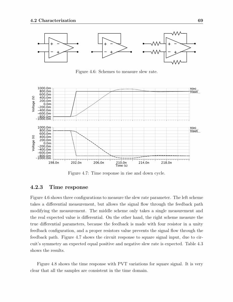
4.2 Characterization 69
+
+
+
+
+
+
Figure 4.6: Schemes to measure slew rate.
Figure 4.7: Time response in rise and down cycle.
4.2.3 Time response
Figure 4.6 shows three configurations to measure the slew rate parameter. The left scheme
takes a differential measurement, but allows the signal flow through the feedback path
modifying the measurement. The middle scheme only takes a single measurement and
the real expected value is differential. On the other hand, the right scheme measure the
true differential parameters, because the feedback is made with four resistor in a unity
feedback configuration, and a proper resistors value prevents the signal flow through the
feedback path. Figure 4.7 shows the circuit response to square signal input, due to cir-
cuit’s symmetry an expected equal positive and negative slew rate is expected. Table 4.3
shows the results.
Figure 4.8 shows the time response with PVT variations for square signal. It is very
clear that all the samples are consistent in the time domain.

70 High Input Swing, Gain, and CMRR Robust OTA
Specification Result
SR+ [V/µs] 232SR- [V/µs] 233
Settling time (0.1%) [ns] 19Overshoot [V] 0.1
Table 4.3: Time response results.
Figure 4.8: PVT simulation over step response.
4.2.4 CMRR
Under typical conditions the measurement of differential Common Mode Rejection Ratio
(CMRR) is wrong, because the ideal operation and signal subtraction produces an ideal
measurement. One option is to measure the single output instead of the differential, and
divide the differential gain by the measured value. But this type of measurement is only
useful to obtain an approximate value, for this reason the best choice is to perform a
monte-carlo analysis, in which the differential output is a realistic value, and the differen-
tial gain could be divided by the measurement obtaining a real value.
Figure 4.9 shows the measurement on a single output. The result for low frequency is
very good, and the frequency range of interest remains a high value. Figure 4.10 shows
the histogram for 200 simulations in the monte-carlo analysis, in which was observed a
trend between 140 and 170 dB. The results of the monte-carlo analysis are so positive
because more than 80% of the samples are upper 100 dB, and the average value is 150
dB.

4.2 Characterization 71
Figure 4.9: CMRR single measurement.
20 40 60 80 100 120 140 160 180 200 2200
10
20
30
40
50
CMRR (dB)
Sa
mp
les
Figure 4.10: CMRR measurement with monte-carlo analysis.
The outstanding result for CMRR specification (including mismatch) is due to the
wide use of the FDP cell, it is because using this structure is more difficult that the
transistors get out form the desired operation point, and the correct biasing remain despite
process variations. Also, the stability of the transconductance and the explained design
considerations makes that the variations have not high impact on this specification. These
reasons are also valid to explain the conclusive measurements over the next specification.

72 High Input Swing, Gain, and CMRR Robust OTA
Figure 4.11: Samples of PSRR measurement.
40 45 50 55 60 65 70 750
50
100
150
200
PSRR+ (dB)
Sam
ple
s
(a)
50 55 60 65 70 75 80 850
50
100
150
200
PSRR− (dB)
Sa
mp
les
(b)
Figure 4.12: PSRR measurement with monte-carlo analysis.
4.2.5 PSRR
The Power Supply Rejection Ratio (PSRR) measurement was also made through monte-
carlo analysis in order to obtain realistic values for this specification. Figure 4.11 shows
a couple of samples for positive and negative PSRR measurements to show the frequency
response of this specification. Figures 4.12(a) and 4.12(b) shows the histogram for 200
simulations, in each case the result is extremely conclusive with respect to the value of
the specification, for both cases it is 60 dB.

4.2 Characterization 73
Figure 4.13: Input referred noise.
4.2.6 Noise
Figure 4.13 shows the input referred noise in the two major units of measurement, the
result is positive since the thermal noise is equivalent to 17 nV/√Hz, which is a low
value taking into account the noise level of the low noise amplifiers. Also, this result is
consistent with the noise levels shown in the technology documentation.
4.2.7 Distortion
A big concern for this type of technology is the distortion parameter, because the tran-
sistor parameters are being modifying along the time axis. This kind of distortion occurs
due to the floating body and its effects, as explained in chapter 1. For this reason the
design was modified and the size of transistors M35,43,36,42 was changed. To this circuit is
proposed a maximum distortion of 0.8% for the maximum output voltage (1.2 Vpp).
Figure 4.14 shows some measurements of distortion with respect to the signal’s ma-
ximum output voltage, this measure was made for a sinusoidal input signal with f=100
KHz. For all the output voltages of the defined output range, the distortion value is less
than 0.8%. Figure 4.15 shows the distortion for signals with f=1 MHz, although the fre-
quency is higher with respect to the previous measure, the result is better since the output
voltage reached higher values with less distortion. For all cases, the spectrum shows that

74 High Input Swing, Gain, and CMRR Robust OTA
0.4 0.5 0.6 0.7 0.8 0.9 1 1.110
−2
10−1
100
Output peak to peak voltage (V)
Dis
tort
ion (
%)
F=100 KHz
Figure 4.14: Distortion vs Output range curve (f=100 KHz).
0.7 0.8 0.9 1 1.1 1.2 1.3 1.410
−1
100
Output peak to peak voltage (V)
Dis
tort
ion
(%
)
f=1 MHz
Figure 4.15: Distortion vs Output range curve (f=1 MHz).
the second harmonic component is eliminated by the differential operation (also all even
components), and the major contribution to distortion is made by the third harmonic.
Third harmonic elimination schemes can be used to reduce the same component (third
harmonic) in order to create a high linear amplifier.
4.2.8 Offset
Finally, figure 4.16 shows the histogram of monte-carlo simulation for the offset mea-
surement, it is clear that the mismatch between differential pairs generates an equivalent

4.2 Characterization 75
0 0.1 0.2 0.3 0.4 0.5 0.6 0.7 0.8 0.9 1
x 10−3
0
50
100
150
200
Input referred offset (V)
Sam
ple
s
Figure 4.16: Offset measurement with monte-carlo analysis.
signal which is amplified in the high impedance nodes, generating imbalance between the
positive and negative outputs, therefore a considerable offset value of 940 µV referred at
the input is obtained. This is one of the few disadvantages that involves the extensive
use of differential pair structures since the mismatch between differential pair transistors
generates high offset values, but in the literature there are several techniques to reduce
the offset value.
Table 4.4 summarize the OTA specifications, the result demonstrate that it is possible
to develop useful specifications for amplifiers in nanometer SOI technologies. In addition,
it was verified that the designed input stage could be integrated in a simple way providing
full input swing. This is the first work of its type reported with 1 V on supply voltage,
because the previous works [3, 9] in the same technology used 1.3 V. The obtained diffe-
rential gain doubles the value obtained in [3] including the attenuation produced by the
input stage. Other outstanding specifications are related with the rejection ratios and
noise, the obtained values were validated through monte-carlo simulations, and indicate
that all the external factors which could harm the signal are very faint. The power con-
sumption is relatively high because a robust circuit always involves additional branches
in order to control or compensate the variations, this is the trade-off for robust circuits.
The next chapter will summarize the main conclusions and proposals obtained in this
work and at the same time will propose suggestions in order to improve or expand this
work.

76 High Input Swing, Gain, and CMRR Robust OTA
Specification Value
Supply voltage 1 VDifferential gain 60 dB
GBW 350 MHzPhase margin 53o
Load capacitance 200 fFDifferential output range 1.2 V
Slew rate 232 V/µsPower consumption 2.6 mW
Settling time @ 0.1% 19 nsCMRR 150 dB
PSRR+,− 60 dBICMR Full swing
Input referred noise 17 nV/√Hz
THD @ Voutdiff =1.2, f=1 MHz 0.25%Input referred Offset 1 mV
Table 4.4: Final OTA specifications

Chapter 5
Conclusions and Future Work
The previous chapters have provided important information about how analog design
can remain in nanometer technologies. There are the two main concerns in nanometer
technologies: the transistors in this type of technologies are not suitable to develop use-
ful specifications in analog circuits like amplifiers; with smaller sizes on transistors, the
uncertainty in fabrication processes, environmental conditions and second order effects,
the variability in the circuit specifications raises significantly. Considering the above two
concerns, the below summarizes the main contributions of this work and how it can be
expanded upon and improved.
5.1 Conclusions
This work proposed and also exposed some circuits, criteria and considerations, in order
to obtain robust and useful specifications for OTA’S. However, the propositions made can
easily be expanded and applied to different circuits, to improve behavior, regardless of
technology type and scale, as outlined below.
A new topology for rail-to-rail input stage with constant transconductance was
proposed. The transconductance and gain specifications are robust regardless of
common mode input voltage or PVT variations. Moreover, this stage can operate
properly over the complete input range (100% of available voltage) with a extremely
minimum change in output common mode voltage. For these reason this stage can
be implemented or integrated in almost all amplifiers.
A new way to obtain constant and robust transconductance was proposed, it is the
emulation of current switching through feedback differential pairs, feedback current
mirrors, and sub-threshold operation to reduce the changes produced by process

78 Conclusions and Future Work
and voltage variations. Also, the use of stages with opposite behavior with respect
to temperature in order to compensate its effects.
A cause was determined for low frequency gain variation in the flat-band of amplifiers
made in SOI nanometer technology. In the same way, an effective solution through
body-contact transistors in specific connections was proposed.
The usefulness of matrix transistors in nanometer technologies was verified, in order
to improve the behavior with respect to mismatch, PVT and SCE. Also, it was
determined that matrix transistors contribute to reduce the low frequency gain
variation, and are the only choice to obtain different transistor sizes in technologies
with several restrictions in transistor sizing.
A new high gain OTA scheme without cascode structures was proposed. This scheme
obtained 67 dB with only two stages in 45 nanometer technology, this gain value
is comparable with conventional two stages amplifiers in micrometer technologies.
Despite high gain value, others specifications such as GBW or power consumption
were not significantly affected.
Additional considerations to achieve robust gain stages with respect to commonly
techniques were proposed.
Besides the widely known benefits of the FDP structure, it was verified that this
structure improves the circuit performance with respect to PVT variations and
allows the use of more complex current mirror structures without reducing dynamic
range.
Although the aim of this work focuses on PVT variations, the same techniques and
schemes proved its efficiency including mismatch for some specifications.
With the easy integration of the input and gain stages, the use of input stage to
provide in a easy way full input swing, with any changes in transistors sizing was
verified.
The final specifications shows that robust amplifiers with good performance in all
the specifications for nanometer SOI technologies could be developed.

5.2 Future Work 79
5.2 Future Work
With the development of this work arises new interesting topics to complement and en-
hance the current work. On the other hand, some tasks, simulations and analysis must
be done to finish the design flow for analog circuits in nanometer technologies. There are:
It will be necessary to study and characterize the body section in body-contact
transistors to analyze its feasibility in different applications such as CMFB, ampli-
fiers, special filters (logarithmic) and multipliers among others. On the other hand
conducting a deepest analysis over the charge variation along time in the body and
its effects over different circuits is also suggested.
Due to the technology restricted sizing the layout stage represents a big concern.
This is due to the technology incorporating many more layers than conventional
technologies and the use of matrix transistors, which raises the complexity in the
layout stage. However, the restrictions over the sizing could allow the automation
of the layout in a similar way to that of digital circuits.
Establish some criteria in other types of circuits that allows the making of a robust
design in a clearer way.
During the design and simulation with the SC-CMFB circuit it was observed that
the couple of noise in the signal due to the switching it is not negligible. In signal
processing circuits that employes switched capacitor must be carefully designed in
order to avoid noise and distortion. On the other hand, the low available voltage
causes some switches not to work properly and in circuits of precision this issue
cannot be neglected.
The most common way to try to compensate analog circuits is through biasing, for
this reason it is desirable to develop a variety of biasing circuits widely characterized
in order to make easy and fast compensations in any design.
Incorporate some techniques in order to reduce the circuit offset, and try to reduce
the power consumption without losing robustness.

Bibliography
[1] Y. Nishi and R. Doering, Handbook of semiconductor manufacturing technology.
Marcel Dekker, 2000.
[2] D. C. C. Modeling, SOI12S0 Model Reference Guide, ser. IBM Microelectronics Di-
vision. IBM Corporation, 2008.
[3] H. Gomez, “Robust to PVT, High DC Gain Amplifier for CT Σ∆ Modulators,” Mas-
ter’s thesis, Instituto Nacional de Astrofısica Optica y Electronica, Puebla, Mexico,
2011.
[4] J. M. Rabaey, A. Chandrakasan, and B. Nikolic, Digital integrated circuits- A design
perspective, 2nd ed. Prentice Hall, 2004.
[5] B. Razavi, Design of Analog CMOS Integrated Circuits, 1st ed. New York, NY,
USA: McGraw-Hill, Inc., 2001.
[6] K. Roy, S. Mukhopadhyay, and H. Mahmoodi-Meimand, “Leakage current mech-
anisms and leakage reduction techniques in deep-submicrometer CMOS circuits,”
Proceedings of the IEEE, vol. 91, no. 2, pp. 305 – 327, February 2003.
[7] K. Bernstein and N. J. Rohrer, SOI Circuit Design Concepts, 1st ed. Springer
Publishing Company, Incorporated, 2007.
[8] J. Kuo and S. Lin, Low-voltage SOI CMOS VLSI devices and circuits, ser. A Wiley-
interscience publication. Wiley, 2001.
[9] R. Astro, “A PVT Compensated Active Inductor Based VCO on SOI CMOS Techno-
logy,” Master’s thesis, Instituto Nacional de Astrofısica Optica y Electronica, Puebla,
Mexico, 2011.

BIBLIOGRAPHY 81
[10] F. Silveira, D. Flandre, and P. Jespers, “A gm/ID based methodology for the design
of CMOS analog circuits and its application to the synthesis of a silicon-on-insulator
micropower OTA,” Solid-State Circuits, IEEE Journal of, vol. 31, no. 9, pp. 1314 –
1319, September 1996.
[11] O. Berntsen, C. Wulff, and T. Ytterdal, “High speed, high gain OTA in a digital 90nm
CMOS technology,” NORCHIP Conference, 2005. 23rd, pp. 129 – 132, November
2005.
[12] S. dela Cruz, M. delos Reyes, T. Gaffud, T. Abaya, M. Gusad, and M. Rosales,
“Design and implementation of operational amplifiers with programmable characte-
ristics in a 90nm CMOS process,” Circuit Theory and Design, 2009. ECCTD 2009.
European Conference on, pp. 209 – 212, August 2009.
[13] M. Taherzadeh-Sani and A. A. Hamoui, “A 1-V Process-Insensitive Current-Scalable
Two-Stage Opamp With Enhanced DC Gain and Settling Behavior in 65-nm Digital
CMOS,” Solid-State Circuits, IEEE Journal of, vol. 46, no. 3, pp. 660 – 668, March
2011.
[14] S. Mirhosseini and A. Ayatollahi, “A Low-Voltage, Low-Power, Two-Stage Amplifier
for Switched-Capacitor Applications in 90 nm CMOS Process,” Iranian Journal of
Electrical & Electronic Engineering, vol. 6, no. 4, December 2010.
[15] C. Galup-Montoro, M. Schneider, and I. Loss, “Series-parallel association of FET’s
for high gain and high frequency applications,” Solid-State Circuits, IEEE Journal
of, vol. 29, no. 9, pp. 1094 – 1101, September 1994.
[16] R. Fiorelli, A. Arnaud, and C. Galup-Montoro, “Series-parallel association of tran-
sistors for the reduction of random offset in non-unity gain current mirrors,” Circuits
and Systems, 2004. ISCAS ’04. Proceedings of the 2004 International Symposium on,
vol. 1, May 2004.
[17] R. J. Baker, CMOS Circuit Design, Layout, and Simulation, 3rd ed. Wiley-IEEE
Press, 2010.
[18] M. Sanz, S. Celma, B. Calvo, and D. Flandre, “Self-cascode SOI versus graded-
channel SOI MOS transistors,” Circuits, Devices and Systems, IEE Proceedings -,
vol. 153, no. 5, October 2006.
[19] E. Sanchez-Sinencio, “Rail to Rail Op Amps,” TAMU-AMSC, [Online] Avali-
able:http://amesp02.tamu.edu/ sanchez/607%20Lect%205-Rail2Rail-2008.pdf.

82 BIBLIOGRAPHY
[20] Y. Lu and R. Yao, “Low-voltage constant-gm rail-to-rail CMOS operational amplifier
input stage,” Elsevier Solid-State Electronics, vol. 52, pp. 957 – 961, March 2008.
[21] B. Minch, “A simple way to extend the common-mode input-voltage range of the
MOS differential pair,” Circuits and Systems, 2002. MWSCAS-2002. The 2002 45th
Midwest Symposium on, vol. 1, pp. 97 – 100, August 2002.
[22] I. Padilla, J. Ramirez-Angulo, R. Carvajal, and A. Lopez-Martin, “Low voltage rail-
to-rail operational amplifier based on flipped voltage followers,” Circuits and Systems,
2005. 48th Midwest Symposium on, vol. 1, pp. 267 – 270, August 2005.
[23] S. Tongyu, H. Jingyu, L. Xiaohong, E. Sanchez-Sinencio, and Y. Shouli, “A Robust
and Scalable Constant- Rail-to-Rail CMOS Input Stage With Dynamic Feedback for
VLSI Cell Libraries,” Circuits and Systems I: Regular Papers, IEEE Transactions
on, vol. 55, no. 3, April 2008.
[24] A. Masoom and K. Hadidi, “A 1.5-V, Constant-Gm, Rail-to-Rail Input Stage Oper-
ational Amplifier,” Electronics, Circuits and Systems, 2006. ICECS ’06. 13th IEEE
International Conference on, pp. 632 – 635, December 2006.
[25] L. Yan and H. Ruo, “Low-voltage constant-gm rail-to-rail CMOS operational ampli-
fier input stage,” Solid-State Electronics - ELSEVIER, pp. 957 – 961, March 2008.
[26] S. Tongyu and Y. Shouli, “A Robust Rail-to-Rail Input Stage with Constant-gm
and Constant Slew Rate Using a Novel Level Shifter,” Circuits and Systems, 2007.
ISCAS 2007. IEEE International Symposium on, pp. 477 – 480, May 2007.
[27] R. Baker and V. Saxena, “High Speed Op-amp Design: Compensation and Topolo-
gies for Two and Three Stage Designs,” Boise State University, [Online] Avali-
able:http://cmosedu.com/jbaker/papers/talks.
[28] J. Carrillo, G. Torelli, M. Dominguez, R. Perez-Aloe, J. Valverde, and J. Duque-
Carrillo, “A Family of Low-Voltage Bulk-Driven CMOS Continuous-Time CMFB
Circuits,” Circuits and Systems II: Express Briefs, IEEE Transactions on, vol. 57,
no. 11, November 2010.