Embed Size (px)
Citation preview

Application Note QN8027
Rev 0.25 (10/09) Copyright ©2009 by Quintic Corporation Page 1
Confidential B Confidential Information contained herein is covered under Non-Disclosure Agreement (NDA).
QN8027 Hardware Application Note
October, 2009

Hardware Application Note QN8027 ,
Rev 0.25 (10/09) Copyright ©2009 by Quintic Corporation Page 2
Confidential B Confidential Information contained herein is covered under Non-Disclosure Agreement (NDA).
Contents
1 Feature Overview .................................................................................................... 4
1.1 Main Feature for QN8027 .............................................................................................................. 4
2 Hardware Design..................................................................................................... 5
2.1 Power Supply ................................................................................................................................. 5
2.2 Control Interface............................................................................................................................. 5
2.3 Clock Interface ............................................................................................................................... 6
2.4 Audio Input Interface ..................................................................................................................... 7
2.5 Differential Audio Input Reference Circuit.................................................................................... 8
2.6 FM Transmitter Antenna Interface ................................................................................................. 9
2.7 Difference between Qn8000 and QN8027 ................................................................................... 10
2.8 Power Amplifier Circuit for QN8027........................................................................................... 10
2.9 Schematic of QN8027 Reference Design ..................................................................................... 12
2.10 PCB Layout for QN8027.............................................................................................................. 13
2.11 AN Example of PCB Layout ........................................................................................................ 15

Hardware Application Note QN8027 ,
Rev 0.25 (10/09) Copyright ©2009 by Quintic Corporation Page 3
Confidential B Confidential Information contained herein is covered under Non-Disclosure Agreement (NDA).
REVISION HISTORY
REVISION Summary of Changes Date
0.1 Draft. 030109
0.21 Add PA reference circuit 062409
0.22 1. Change ‘FMO’ to ‘RFO’;
2. Add the PA output result, amplify 15dB of the RF power.
062909
0.23 Change the QN8027 SANB reference design. 07/24/2009
0.24
1. In Figure 11: - Add a PA reference design schematic for QN8027 15cm antenna; - Add a note: “If VCC is in the range +2.8V~+3.3V, VIO may directly connect to VCC (pin3), if the voltage for VIO pin is bigger than +3.6V QN8027 will be damaged” on the reference schematic near the VIO pin - Add a note: “ the bypass ripple cap C01 & C02 may be placed as near as possible to pin3 when pcb layout” on the reference schematic near the capacitor C01 & C02 - Add a note “it may be placed as near as possible to pin5 to reduce the parasitical inductor when pcb layout, the parasitical inductor may influence L4 value, ctm may fine tune L4 value from 100nH to 150nH to see which one is the best”. On the reference schematic near the inductor L4
2. Add PCB layout guide in Section 2.11
08/31/2009
0.25
1. Correct a mistake about the PACAP calibration result on page 9. Change from 0x3f~0x00 to 0x1f~0x00;
2. Replace the Figure 1; 3. Modify the grammar and syntax.
10/22/2009
Important Notice
The material contained in this document is provided “as is” and is subject to change, without notice, in future editions. Further, to the maximum extent permitted by applicable law, Quintic disclaims all warranties, either express or implied, with regard to this manual and any information contained herein, including but not limited to the implied warranties of merchantability and fitness for a particular purpose. Quintic shall not be liable for errors or for incidental or consequential damages in connection with the furnishing, use, or performance of this document or of any information contained herein. Should Quintic and the user have a separate written agreement with warranty terms covering the material in this document that conflict with these terms, the warranty terms in the separate agreement shall control.
Hardware Application Note QN8027 ,
Rev 0.25 (10/09) Copyright ©2009 by Quintic Corporation Page 4
Confidential B Confidential Information contained herein is covered under Non-Disclosure Agreement (NDA).
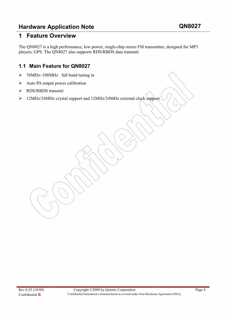
1 Feature Overview
The QN8027 is a high performance, low power, single-chip stereo FM transmitter, designed for MP3
players, GPS. The QN8027 also supports RDS/RBDS data transmit.
1.1 Main Feature for QN8027
� 76MHz~108MHz full band tuning in
� Auto PA output power calibration
� RDS/RBDS transmit
� 12MHz/24MHz crystal support and 12MHz/24MHz external clock support

Hardware Application Note QN8027 ,
Rev 0.25 (10/09) Copyright ©2009 by Quintic Corporation Page 5
Confidential B Confidential Information contained herein is covered under Non-Disclosure Agreement (NDA).
2 Hardware Design
This chapter describes the details of hardware design and schematic of reference design.
2.1 Power Supply
QN8027 is integrated LDO inside, and the VCC accepts the power supply voltage range from
2.7V~5.0V.
QN8027 has a pin ‘VIO’ which is used to define the I/O high voltage level. ‘VIO’ only accepts the
voltage range 2.7V~3.3V.
The VCC power supply should be not larger than 3.3V, so that VCC and VIO can be connected together
directly with the power supply. If the VCC power supply is larger than 3.3V, VIO should be connected
with 3.3V voltage solely.
2.2 Control Interface
QN8027 uses I2C bus to communication only. And I
2C process follows I
2C protocol.
QN8027 I2C device address (7 bits) is 0x2C (0101100). When it comes to writing operation, it should be
added ‘0’ as the LSB of the address (0x58); when it comes to reading operation, it should be add ‘1’ as
the LSB of the address (0x59).
SDA pin is the data bus and SCL pin is the clock bus, on these two buses, the pull up registers are
needed. And the registers values should be adjusted according to the I2C rate.
I2C Write Operation
I2C Read Operation
SCL
SDA
Data Byte 2 ACK by
QN8027
ACK by ACK by
QN8027
Data Byte 3 Data Byte n Stop
QN8027 QN8027 QN8027
Start I2C slave Address R/W ACK by Base Address Data Byte 1ACK by ACK by
A7 A6 A5 A4 A3 A2 A1 A0 D7 D6 D5 D4 D3 D2 D1 D0
SCL
SDA
SCL
SDA
SCL
SDA
A7 A6 A5 A4 A3 A2 A1 A0
QN8027 QN8027
Start I2C slave Address R/W ACK by Base Address ACK by Stop
D7 D6 D5 D4 D3 D2 D1 D0 D7 D6 D5 D4 D3 D2 D1 D0
QN8027 micro
Start I2C slave Address R/W ACK by ACK by StopData Byte 1 Data Byte n
micro
ACK by
D7 D6 D5 D4 D3 D2 D1 D0D7 D6 D5 D4 D3 D2 D1 D0D7 D6 D5 D4 D3 D2 D1 D0
QN8027
Figure 1. I2C Write and Read Operation Timing

Hardware Application Note QN8027 ,
Rev 0.25 (10/09) Copyright ©2009 by Quintic Corporation Page 6
Confidential B Confidential Information contained herein is covered under Non-Disclosure Agreement (NDA).
2.3 Clock Interface
Pin 1’XTAL2’ and pin 2 ‘XTAL1’ are used to crystal input. QN8027 accepts 12MHz and 24MHz crystals. And the crystals need 20pF load cap. The chip default setting is 24MHz crystal. If the crystal is
changed, it needs to change some registers and recalibrate to make chip for the crystal setting.
Figure 2. Crystal Input Interface
QN8027 accepts external clock input. It accepts square clock with the voltage range 0~UVIO and sin
wave single-end and sin wave differential clock input (Figure 3). For sin wave single-end clock input,
the voltage of the clock should be larger than 350mVpeak. With differential sin wave clock input, the
clock input voltage should larger than 350mVp-p every endpoint (Figure 4).
If used external clock, XTAL1 pin is used to clock input.
Figure 3. Square Wave Clock Input Interface
Figure 4. Sin Wave Clock Input Interface

Hardware Application Note QN8027 ,
Rev 0.25 (10/09) Copyright ©2009 by Quintic Corporation Page 7
Confidential B Confidential Information contained herein is covered under Non-Disclosure Agreement (NDA).
2.4 Audio Input Interface
QN8027 has integrated VGA inside which can change the input impedance of 5k ohm, 10k ohm, 20k ohm and 40k ohm by registers control.
With default register setting, audio input only accepts maximum 1000mVp-p voltage. And audio input
needs a capacitor to separate DC voltage. The suggested capacitor value is 4.7uF.
Figure 5. Audio Input Interface
Figure 6. Audio Input 1000mVp-p voltage
From the Figure 5 and Figure 6, the capacitor and the import impedance build up a high pass filter
structure. And the low cut-off frequency is: ; in order to get a good frequency response at low
frequency, the capacitor value is suggested to 4.7uF.
Hardware Application Note QN8027 ,
Rev 0.25 (10/09) Copyright ©2009 by Quintic Corporation Page 8
Confidential B Confidential Information contained herein is covered under Non-Disclosure Agreement (NDA).
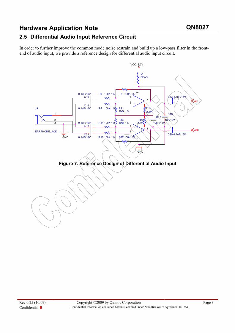
2.5 Differential Audio Input Reference Circuit
In order to further improve the common mode noise restrain and build up a low-pass filter in the front-end of audio input, we provide a reference design for differential audio input circuit.
GND
R5 100K 1%
J9
EARPHONEJACK
1
23
R17 100K 1%
R10
200K
R12200K
C17
10uF/16V
R9100k 1%
R13100k 1%
VCC_3.3V
R6 100K 1%
R14 100K 1%
R16 100K 1%
R8 100K 1%
+
-
31
4
2
C140.1uF/16V
C100.1uF/16V
C180.1uF/16V
L4
BEAD
+
-
57
8
6
C210.1uF/16V
C16
1uF/16V
GND
C13 4.7uF/16V
C20 4.7uF/16V
ALI
ARI
Figure 7. Reference Design of Differential Audio Input

Hardware Application Note QN8027 ,
Rev 0.25 (10/09) Copyright ©2009 by Quintic Corporation Page 9
Confidential B Confidential Information contained herein is covered under Non-Disclosure Agreement (NDA).
2.6 FM Transmitter Antenna Interface
QN8027 uses auto turn for every channel with the integrated adjustable capacitor and can make the PA
output voltage to get maximum value at every channel.
The PA structure of QN8027 needs an inductor at the outside of the chip, which is used to produce a
resonant circuit with the integrated capacitor, and it also provides a DC back circuit for the PA output.
Figure 8. PA output circuit
According to the chip design, the inductor should be assembled as close as possible to the chip.
The integrated capacitor is adjustable and according to the polynomial , in order to covers the
frequency range from 76MHz ~ 108MHz, the 150nH inductor is suggested. And this inductor value will
modify according the equivalent serial capacitor which induct from the board layout and the antenna
type.
To judge whether the inductor has covered the full span, reg30 can be used. Set the RF frequency of
76MHz and read the reg30 value, then set RF frequency of 108MHz and read reg30 value, if both two
reg30 values are in range 0x1f~0x00, it means the inductor can cover the full span. Otherwise, it is
necessary to change the inductor value to cover the full span.

Hardware Application Note QN8027 ,
Rev 0.25 (10/09) Copyright ©2009 by Quintic Corporation Page 10
Confidential B Confidential Information contained herein is covered under Non-Disclosure Agreement (NDA).
2.7 Difference between Qn8000 and QN8027
� QN8000 only accepts 7.6MHz crystal; QN8027 accepts 12MHz/24MHz crystal.
� QN8000 uses 2 wire and 3wire control interface; QN8027 only uses I2C control interface. QN8000
and QN8027 have different device ID.
� QN8000 RFO can connect to antenna; QN8027 RFO needs an inductor about 150nH across to GND
nearby the RFO pin.
2.8 Power Amplifier Circuit for QN8027
QN8027 has an integrated power amplifier. If the output power still can’t meet the requirement, it can
be added an external power amplifier outside of the chip RFO pin.
The circuit is shown as following:
RFO
L1120nH
C1
1000pF
R1
0 ohm
R2
100k
L2390nH
C26.5pF
C3
1000pF
C4
1000pF
R3
0 ohm
Q1FHT9018
VCC
75cm ANTENNA
PA reference circuit
Figure 9. External PA Reference Circuit for 75cm Antenna
Hardware Application Note QN8027 ,
Rev 0.25 (10/09) Copyright ©2009 by Quintic Corporation Page 11
Confidential B Confidential Information contained herein is covered under Non-Disclosure Agreement (NDA).
C1
1000pF
C2
6.5pF
C3
1000pF
C4
1000pF
L1100nH
L2390nH
R1
0 ohm
R2
47k
R3
0 ohm
Q1FHT9018
VCC
RFO
15cm ANTENNA
Figure 10. External PA Reference Circuit for 15cm Antenna
*Note: in the Figure 10, RFO connects to the pin 5 of QN8027 directly.
The reference circuit is designed based on QN8027 EVB with the PA circuit, RF output power increases
about 15dB. When the circuit is used on practical product, the parameters of the components need do a
little modify according to the layout of the FM transmitter output trace.

Hardw
are Application N
ote Q
N8027
, Rev 0.25 (10/09)
Copyright ©
2009 by Quintic C
orporation
Page 12 C
onfidential B
Confidential Inform
ation contained herein is covered under Non-D
isclosure Agreem
ent (ND
A).
2.9 Schematic of Q
N8027 R
eference Design
XTAL21
XTAL12
VCC3
GND4
RFO5 SCL 6
SDA 7
VIO 8
ARI 9
ALI 10
QN8027-SANB
U1QN8027SAN
L1 2uH
L2 2uH L32uH
C05 4.7uF/16V
L4150nH
C061000pFR22 0
R04NC
R03NC
VIO
SDA
SCL
C021000pF/16V
C0110uF/16V
C1420pF/16V
C1520pF/16V
VCC
C030.01uF/16V
J5EARPHONEJACK
VIO
SCL
SDA
C04 4.7uF/16V
Y112MHz/24MHz
ANT
12V VCC
RegulatorL5 2uH
C8 C9
Tx antenna option for car transmitter case.
R014.7k
R024.7k
VCC
Antenna matching network option.
Option for earphone
C7 1000pF
/XCLK
XCLK
SDA
SCL
VIO
If external clock source available,connect XTAL2 to ground.
wire antenna case.
ANT_PORT
ANT_PORT
VCC VCC
VIO
MAXMIN
4.2V2.7V
3.6V1.6V
Qn8027 Power Supply
note:If VCC is in the range +2.8V~+3.3V,VIO may directly connect to VCC(pin3),if the voltage for VIO pin is biggerthan +3.6V QN8027 will be damaged
note:The bypass ripple cap C01 & C02may be placed as near as possibleto pin3 when pcb layout
note:
It may be placed as near aspossible to pin5 to reduce the parasitical inductor when pcb layout, the parasitical inductormay influence L4 value, ctm may fine tune L4 value from 100nH to150nH to see which oneis the best
The inductor L4
Figure 11. Schematic of QN8027 Reference Design

Hardware Application Note QN8027 ,
Rev 0.25 (10/09) Copyright ©2009 by Quintic Corporation Page 13
Confidential B Confidential Information contained herein is covered under Non-Disclosure Agreement (NDA).
2.10 PCB Layout for QN8027
The example layout as show in the following:
Figure 12. Top Layer
The RF output inductor should be placed to the chip pin5 and the bypass ripple cap should be placed to
pin3 as close as possible.
Close to the QN8027 chip, there should be a large area of GND copper which help to eradiate the FM
high frequency signal.

Hardware Application Note QN8027 ,
Rev 0.25 (10/09) Copyright ©2009 by Quintic Corporation Page 14
Confidential B Confidential Information contained herein is covered under Non-Disclosure Agreement (NDA).
Figure 13. Bottom Layer
Under the chip and the RF signal trace, there need an integrative GND copper. This copper will help to
increase the high frequency signal integrity and also help to eradiate the FM high frequency signal.

Hardware Application Note QN8027 ,
Rev 0.25 (10/09) Copyright ©2009 by Quintic Corporation Page 15
Confidential B Confidential Information contained herein is covered under Non-Disclosure Agreement (NDA).
2.11 AN Example of PCB Layout
Figure 14. Top Layer

Hardware Application Note QN8027 ,
Rev 0.25 (10/09) Copyright ©2009 by Quintic Corporation Page 16
Confidential B Confidential Information contained herein is covered under Non-Disclosure Agreement (NDA).
Figure 15. Bottom Layer

Hardware Application Note QN8027 ,
Rev 0.25 (10/09) Copyright ©2009 by Quintic Corporation Page 17
Confidential B Confidential Information contained herein is covered under Non-Disclosure Agreement (NDA).
Contact Information Quintic Corporation (USA)
3211 Scott Blvd., Suite 203
Santa Clara, CA 95054
Tel: +1.408.970.8808
Fax: +1.408.970.8829
Email: [email protected]
Web: www.quinticcorp.com
Quintic Microelectronics (China)
Building 8 B-301A Tsinghai Science Park
1st East Zhongguancun Rd, Haidian
Beijing, China 100084
Tel: +86 (10) 8215-1997
Fax: +86 (10) 8215-1570
Web: www.quinticcorp.com
Quintic Microelectronics and Quintic are trademarks of Quintic Corporation. All Rights Reserved.


![Hardware and Software Getting Started - Microchip …ww1.microchip.com/downloads/en/AppNotes/Atmel-41075A...ATmegaS128-STK600 [APPLICATION NOTE] Atmel-41075A-Aero-Hardware and Software](https://img.pdfslide.net/doc/110x75/5ea2b4484193417ff6774d79/hardware-and-software-getting-started-microchip-ww1-atmegas128-stk600-application.jpg)


![Hardware and Software Getting Started - Microchip …ww1.microchip.com/downloads/en/AppNotes/Atmel-41074A...ATmega128A-STK600 [APPLICATION NOTE] Atmel-41074A-Aero-Hardware and Software](https://img.pdfslide.net/doc/110x75/5ea2b536d65e064f756d3ad8/hardware-and-software-getting-started-microchip-ww1-atmega128a-stk600-application.jpg)


![Application Note - ATAN0033ww1.microchip.com/downloads/en/AppNotes/Atmel-9305-ATAK... · 2017. 1. 5. · Atmel ATAN0033 [APPLICATION NOTE] 2 9305A–RKE–01/13 1. Hardware Requirements](https://img.pdfslide.net/doc/110x75/61445898aa0cd638b460cc29/application-note-2017-1-5-atmel-atan0033-application-note-2-9305aarkea0113.jpg)