Embed Size (px)
Citation preview
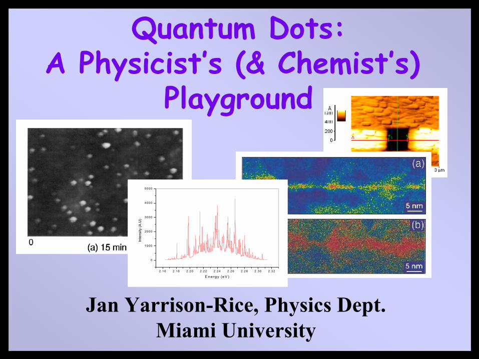
Quantum Dots:A Physicist’s (& Chemist’s)
Playground
Jan Yarrison-Rice, Physics Dept.Miami University
2 .1 6 2 .1 8 2 .2 0 2 .2 2 2 .24 2 .26 2 .2 8 2 .3 0 2 .3 2
0
1 0 00
2 0 00
3 0 00
4 0 00
5 0 00
Inte
nsity
(A.U
)
E n e rg y (e V )
Thanks to Colleagues at University of Cincinnati:
Graduate Students FacultyBob Jones Leigh SmithAditi Sharma Howard JacksonLaurie Robinson
Thanks to Colleagues at Notre Dame:Jacek FurdynaMargaret Dobrowalska
Thanks to NSF and DOE for their support
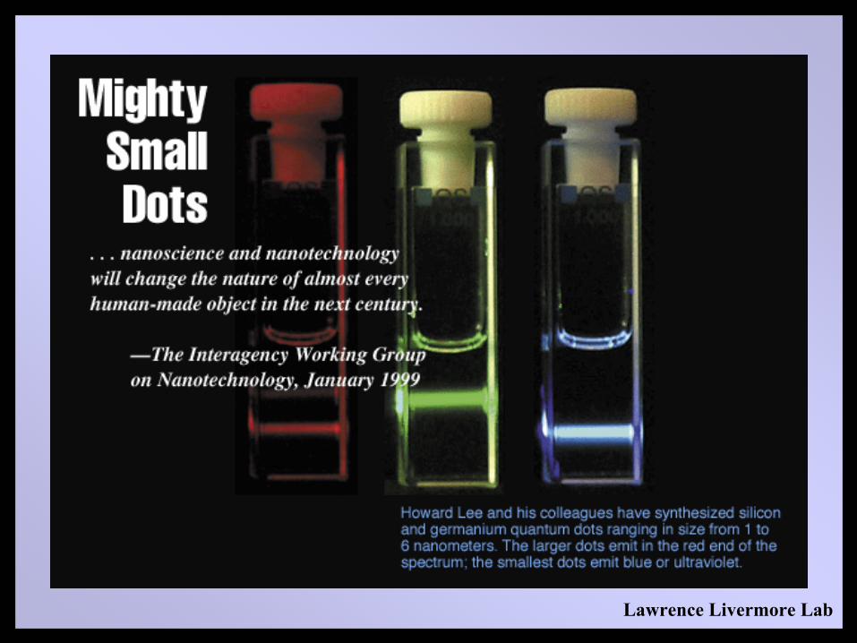
Lawrence Livermore Lab
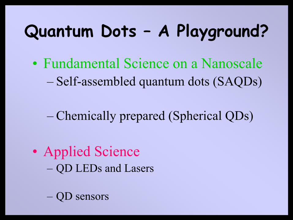
Quantum Dots – A Playground?
• Fundamental Science on a Nanoscale– Self-assembled quantum dots (SAQDs)
– Chemically prepared (Spherical QDs)
• Applied Science– QD LEDs and Lasers
– QD sensors
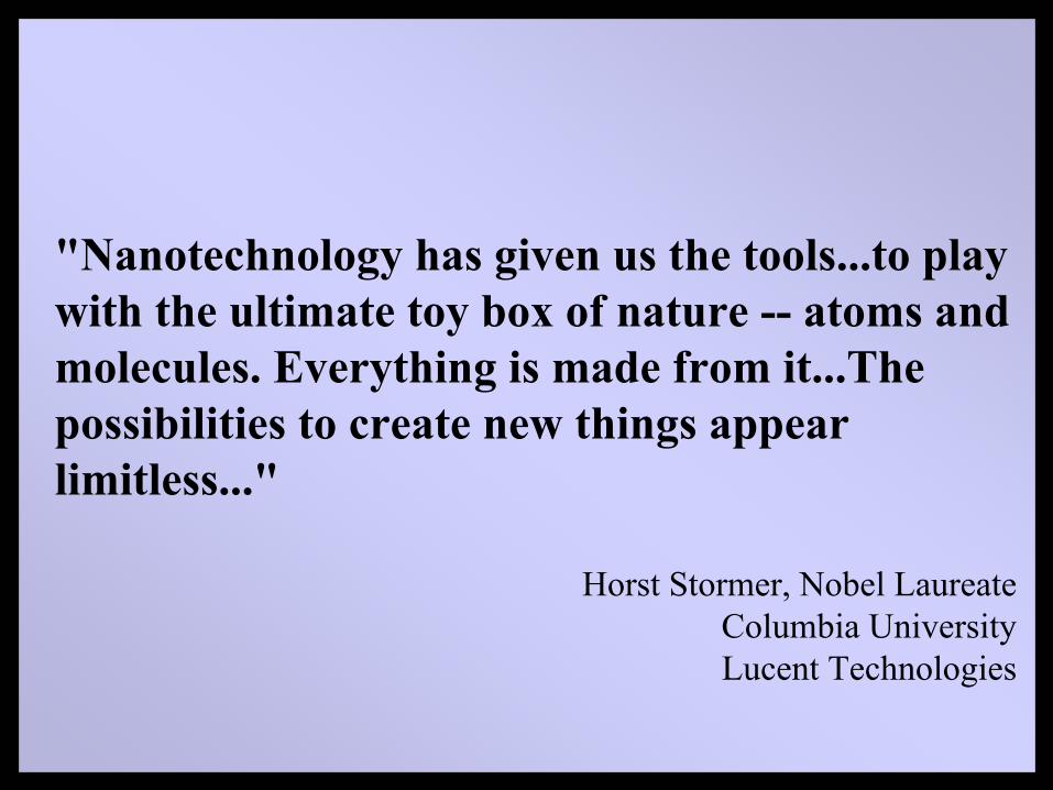
"Nanotechnology has given us the tools...to play with the ultimate toy box of nature -- atoms and molecules. Everything is made from it...The possibilities to create new things appear limitless..."
Horst Stormer, Nobel LaureateColumbia UniversityLucent Technologies
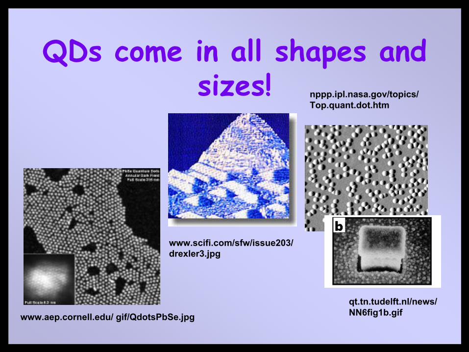
QDs come in all shapes and sizes!
www.aep.cornell.edu/ gif/QdotsPbSe.jpg
www.scifi.com/sfw/issue203/drexler3.jpg
nppp.ipl.nasa.gov/topics/Top.quant.dot.htm
qt.tn.tudelft.nl/news/ NN6fig1b.gif
• To understand the physics of quantum confinement
• Is there anything atomic about “artificial atoms” in a solid?
• Potentials for technology applications
Why Study Semiconductor Quantum Dots?
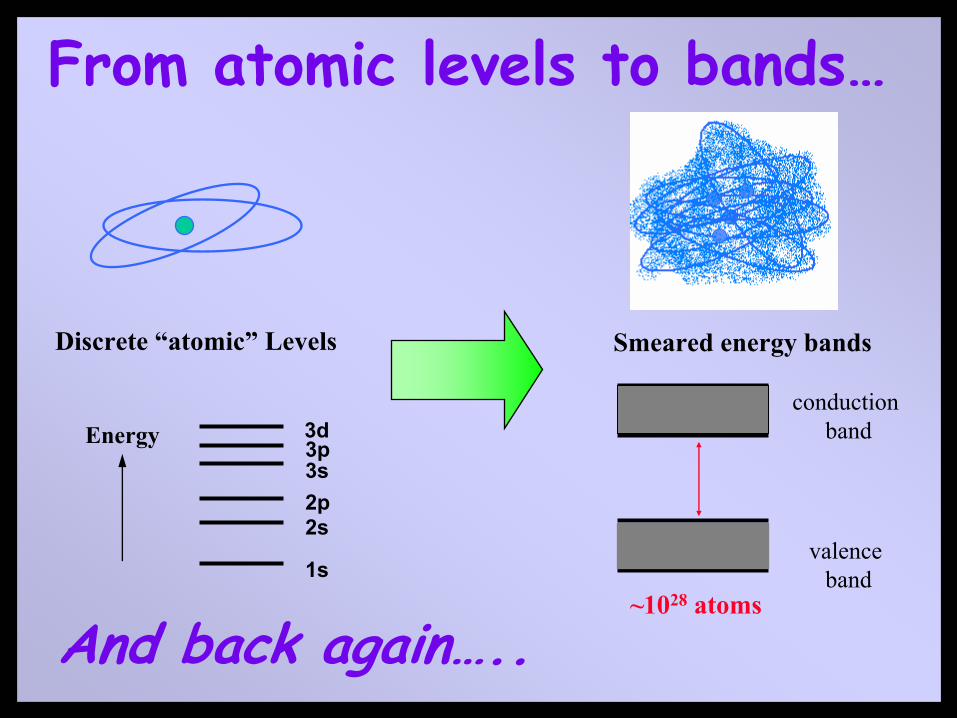
From atomic levels to bands…
Energy
1s
2s2p3s3p3d
~1028 atoms
Discrete “atomic” Levels Smeared energy bands
conduction band
valence band
And back again…..
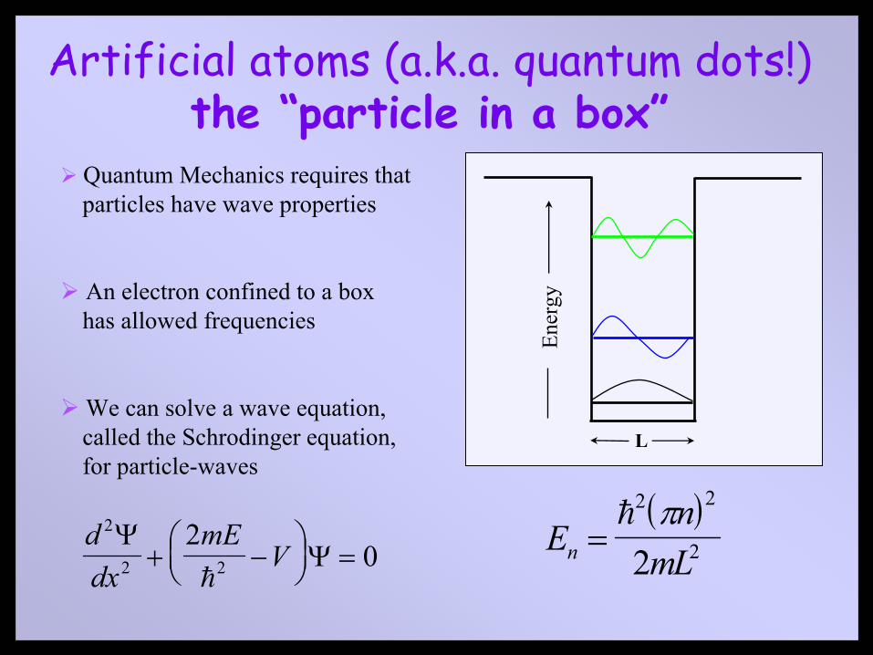
Artificial atoms (a.k.a. quantum dots!)the “particle in a box”
ddx
mEV
2
2 2
20
ΨΨ+ −
=
h
( )E
nmLn =
h2 2
22π
L
Ener
gy
Quantum Mechanics requires that particles have wave properties
An electron confined to a box has allowed frequencies
We can solve a wave equation, called the Schrodinger equation, for particle-waves
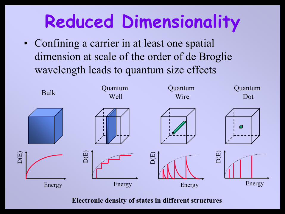
• Confining a carrier in at least one spatial dimension at scale of the order of de Brogliewavelength leads to quantum size effects
Reduced Dimensionality
Electronic density of states in different structures
Energy
D(E
)
Energy
D(E
)
Energy
D(E
)
Energy
D(E
)Bulk
Quantum Well
Quantum Wire
Quantum Dot
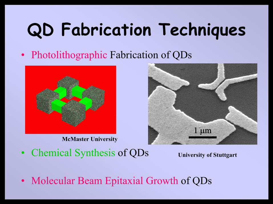
QD Fabrication Techniques• Photolithographic Fabrication of QDs
• Chemical Synthesis of QDs
• Molecular Beam Epitaxial Growth of QDs
McMaster University
University of Stuttgart
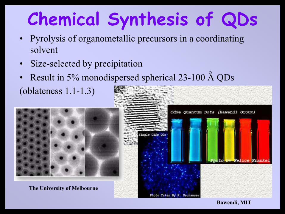
Chemical Synthesis of QDs• Pyrolysis of organometallic precursors in a coordinating
solvent• Size-selected by precipitation• Result in 5% monodispersed spherical 23-100 Α QDs(oblateness 1.1-1.3)
The University of Melbourne
Bawendi, MIT
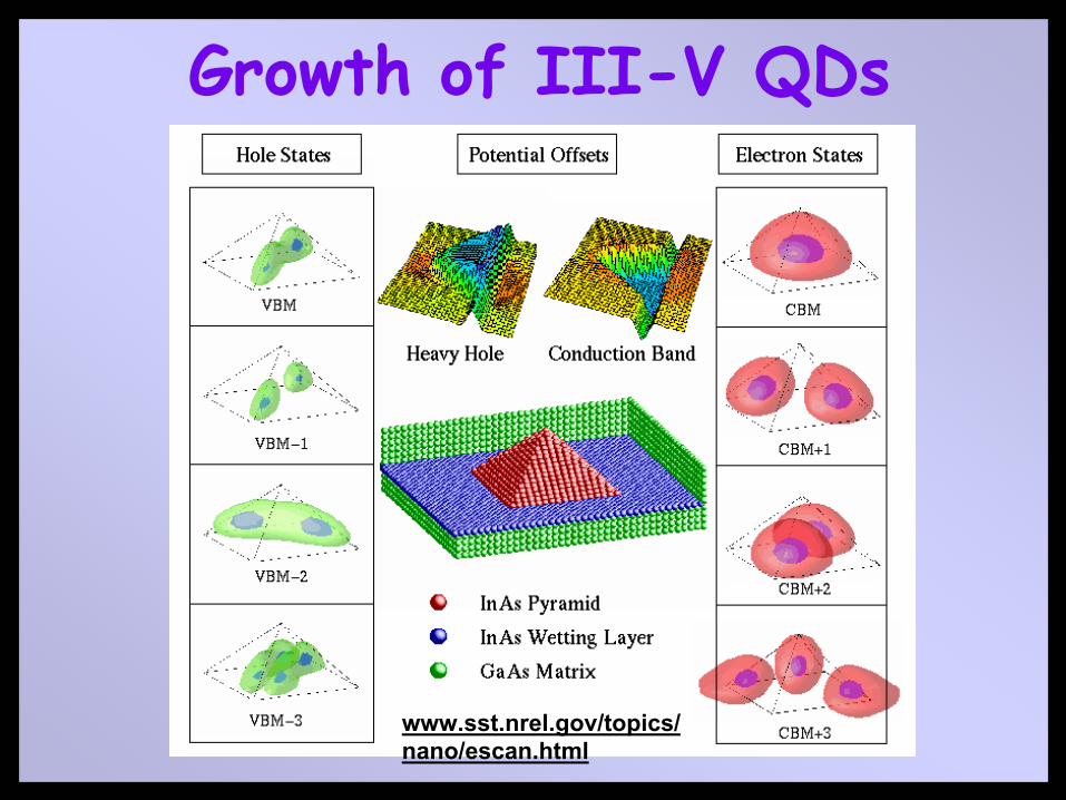
Growth of III-V QDs
www.sst.nrel.gov/topics/ nano/escan.html
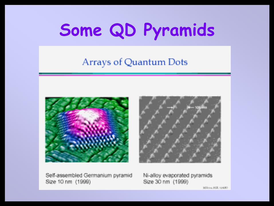
Some QD Pyramids
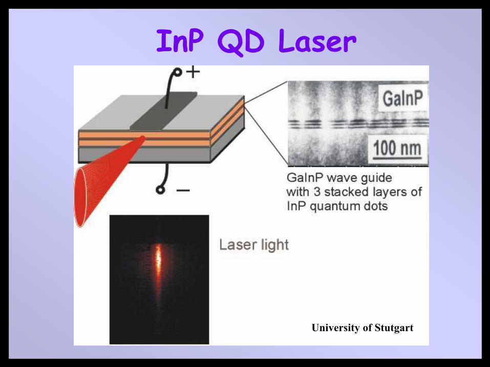
InP QD Laser
University of Stutgart
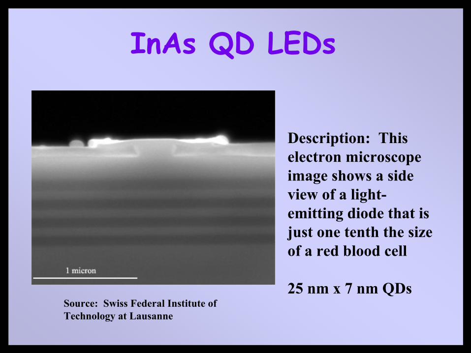
Description: This electron microscope image shows a side view of a light-emitting diode that is just one tenth the size of a red blood cell
25 nm x 7 nm QDsSource: Swiss Federal Institute of Technology at Lausanne
InAs QD LEDs
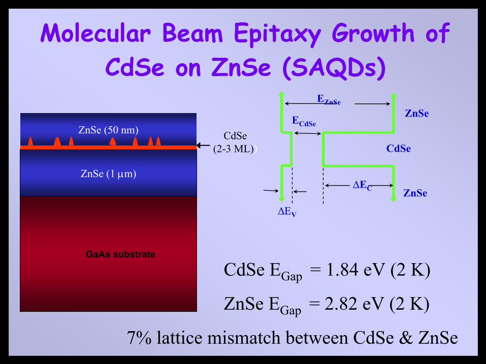
GaAs substrate
ZnSe (1 µm)
ZnSe (50 nm) CdSe(2-3 ML))
Molecular Beam Epitaxy Growth of CdSe on ZnSe (SAQDs)
CdSe EGap = 1.84 eV (2 K)
ZnSe EGap = 2.82 eV (2 K)
7% lattice mismatch between CdSe & ZnSe
ZnSe
CdSe
∆ΕV
ECdSe
ZnSe
EZnSe
∆EC
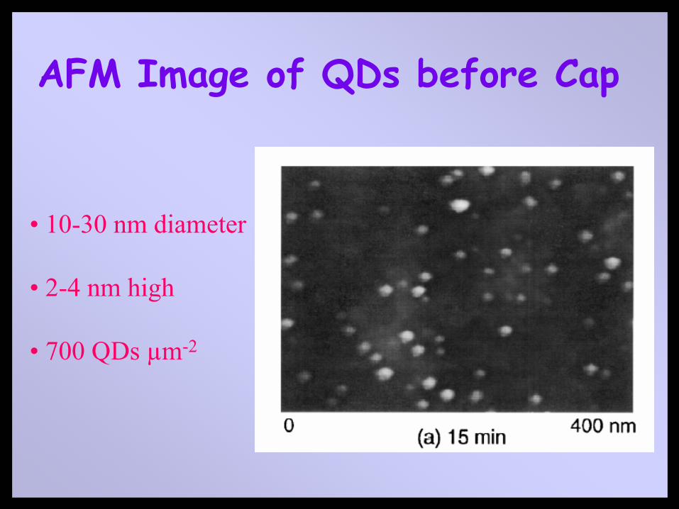
AFM Image of QDs before Cap
• 10-30 nm diameter
• 2-4 nm high
• 700 QDs µm-2
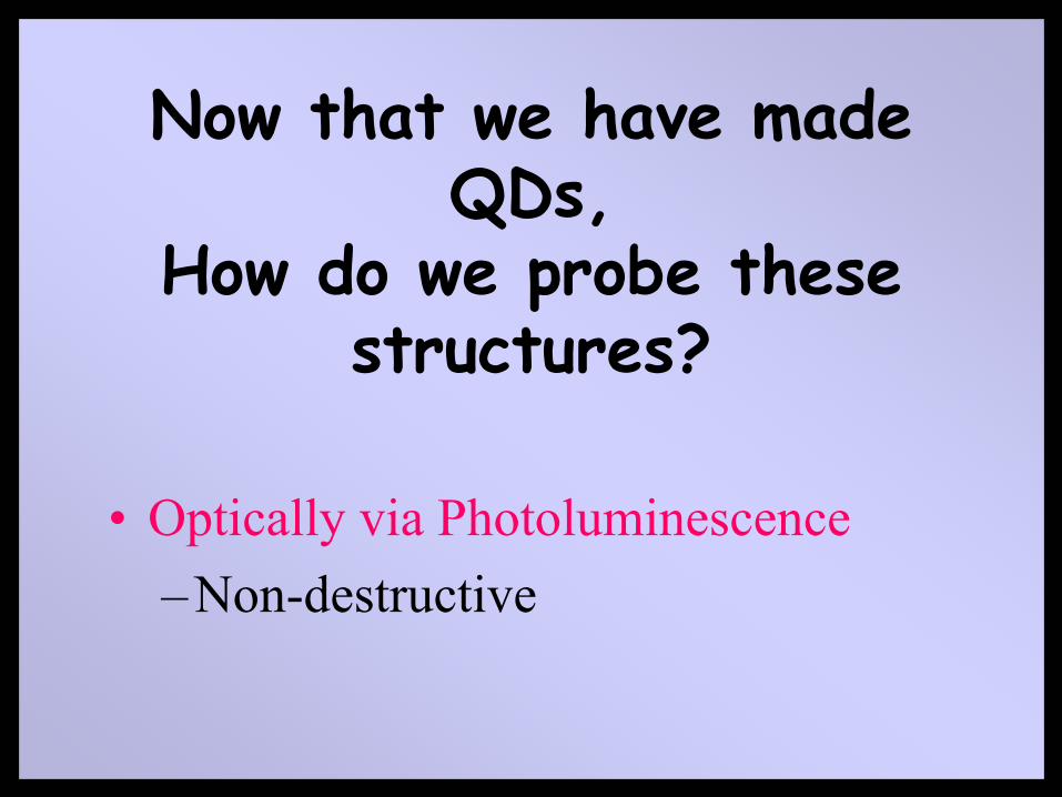
Now that we have made QDs,
How do we probe these structures?
• Optically via Photoluminescence–Non-destructive
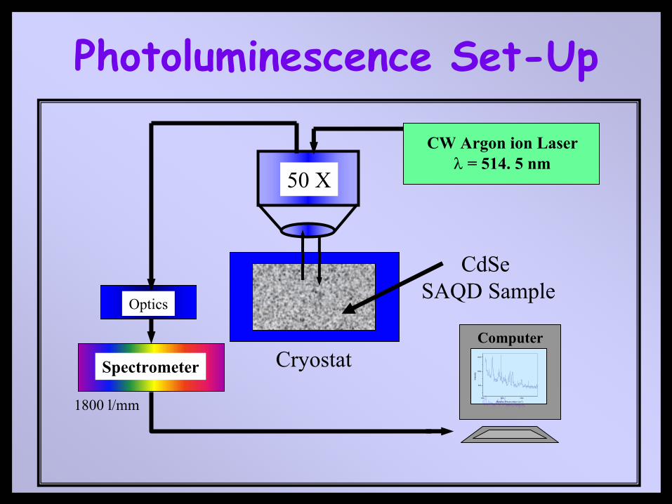
Photoluminescence Set-Up
1300 1400 1500
800
1000
1200
Inte
nsity
Relative Wavenumber (cm-1)
Computer
CW Argon ion Laserλ = 514. 5 nm
CdSeSAQD Sample
Spectrometer
1800 l/mm
Optics
50 X
Cryostat
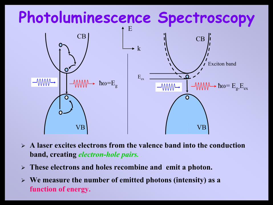
Photoluminescence Spectroscopy
A laser excites electrons from the valence band into the conduction band, creating electron-hole pairs.
These electrons and holes recombine and emit a photon.
We measure the number of emitted photons (intensity) as afunction of energy.
CB
VB
E
k
ħω=Eg
CB
VB
ħω= Eg-Eex
Eex
Exciton band
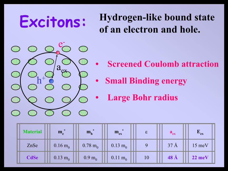
Excitons: Hydrogen-like bound state of an electron and hole.
• Screened Coulomb attraction
• Small Binding energy
• Large Bohr radius
h+aex
e-
Material me* mh
* mex* ε aex Eex
ZnSe 0.16 m0 0.78 m0 0.13 m0 9 37 Å 15 meV
CdSe 0.13 m0 0.9 m0 0.11 m0 10 48 Å 22 meV
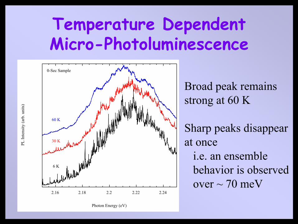
2.16 2.18 2.2 2.22 2.24
PL In
tens
ity (a
rb. u
nits
)
Photon Energy (eV)
6 K
30 K
60 K
0-Sec Sample
Broad peak remainsstrong at 60 K
Sharp peaks disappear at once
i.e. an ensemblebehavior is observedover ~ 70 meV
Temperature Dependent Micro-Photoluminescence
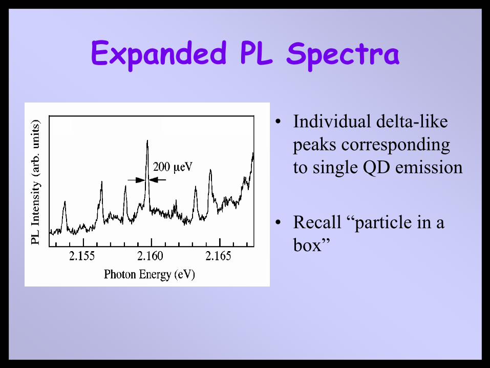
Expanded PL Spectra
• Individual delta-like peaks corresponding to single QD emission
• Recall “particle in a box”
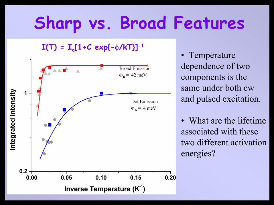
0.00 0.05 0.10 0.15 0.200.2
1Dot EmissionΦD = 4 meV
Broad EmissionΦB = 42 meV
Inverse Temperature (K-1)
Inte
grat
ed In
tens
ity
• Temperature dependence of two components is the same under both cwand pulsed excitation.
• What are the lifetime associated with these two different activation energies?
Sharp vs. Broad FeaturesI(T) = Io[1+C exp{-φ/kT}]-1
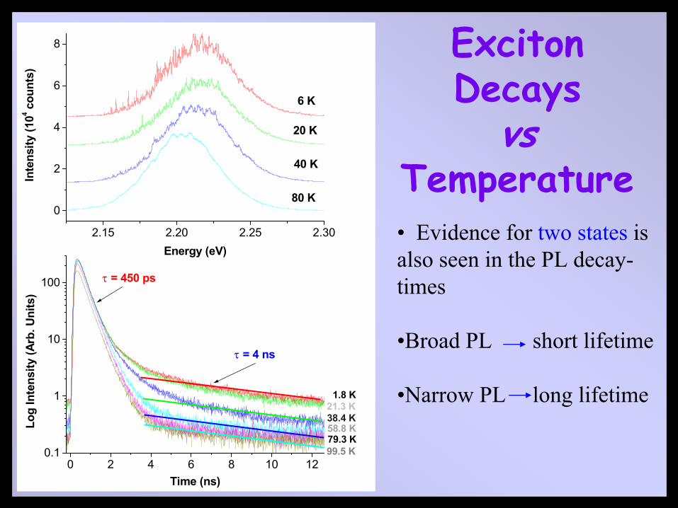
0 2 4 6 8 10 120.1
1
10
100 τ = 450 ps
τ = 4 ns
Log
Inte
nsity
(Arb
. Uni
ts)
Time (ns)
99.5 K79.3 K58.8 K38.4 K21.3 K
1.8 K
2.15 2.20 2.25 2.30
0
2
4
6
8
80 K
40 K
20 K
6 K
Energy (eV)
Inte
nsity
(104 c
ount
s)
• Evidence for two states is also seen in the PL decay-times
•Broad PL short lifetime
•Narrow PL long lifetime
Exciton Decays
vsTemperature
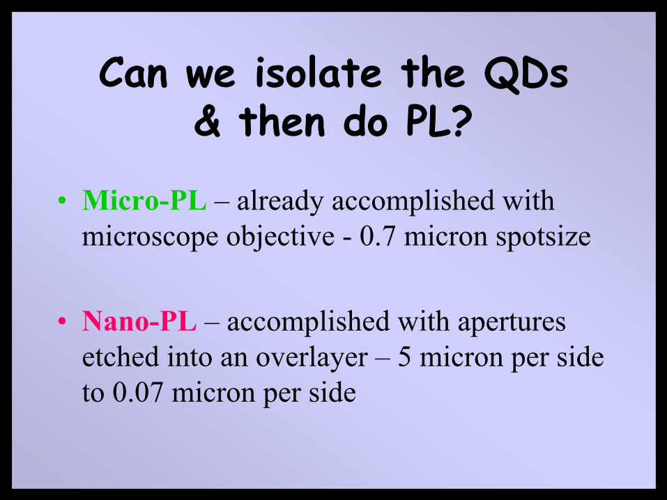
Can we isolate the QDs& then do PL?
• Micro-PL – already accomplished with microscope objective - 0.7 micron spotsize
• Nano-PL – accomplished with apertures etched into an overlayer – 5 micron per side to 0.07 micron per side
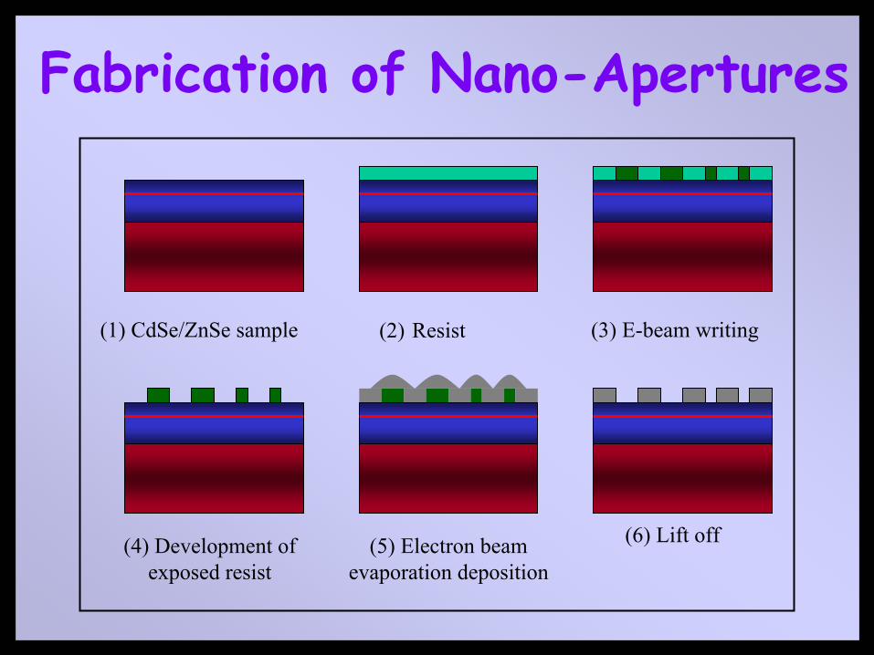
Fabrication of Nano-Apertures
(1) CdSe/ZnSe sample (2) Resist (3) E-beam writing
(4) Development of exposed resist
(5) Electron beam evaporation deposition
(6) Lift off
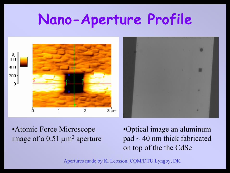
Nano-Aperture Profile
•Atomic Force Microscope image of a 0.51 µm2 aperture
•Optical image an aluminum pad ~ 40 nm thick fabricated on top of the the CdSe
Apertures made by K. Leosson, COM/DTU Lyngby, DK
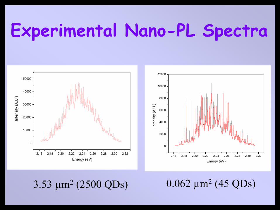
Experimental Nano-PL Spectra
2.16 2.18 2.20 2.22 2.24 2.26 2.28 2.30 2.32
0
10000
20000
30000
40000
50000
Inte
nsity
(A.U
.)
Energy (eV)2.16 2.18 2.20 2.22 2.24 2.26 2.28 2.30 2.32
0
2000
4000
6000
8000
10000
12000
Inte
nsity
(A.U
.)
Energy (eV)
3.53 µm2 (2500 QDs) 0.062 µm2 (45 QDs)
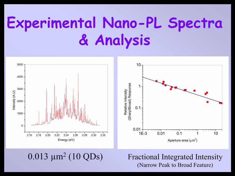
2.16 2.18 2.20 2.22 2.24 2.26 2.28 2.30 2.32
0
1000
2000
3000
4000
5000
Inte
nsity
(A.U
)
Energy (eV)
1E-3 0.01 0.1 1 100.01
0.1
1
10
Rel
ativ
e In
tens
ity
(Sha
rp/B
road
) Res
pons
e
Aperture area (µm2)
0.013 µm2 (10 QDs) Fractional Integrated Intensity(Narrow Peak to Broad Feature)
Experimental Nano-PL Spectra& Analysis
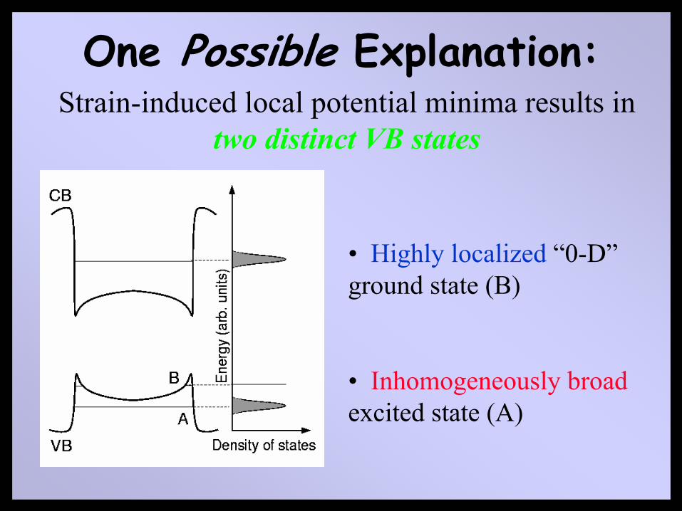
One Possible Explanation:Strain-induced local potential minima results in
two distinct VB states
• Highly localized “0-D” ground state (B)
• Inhomogeneously broadexcited state (A)
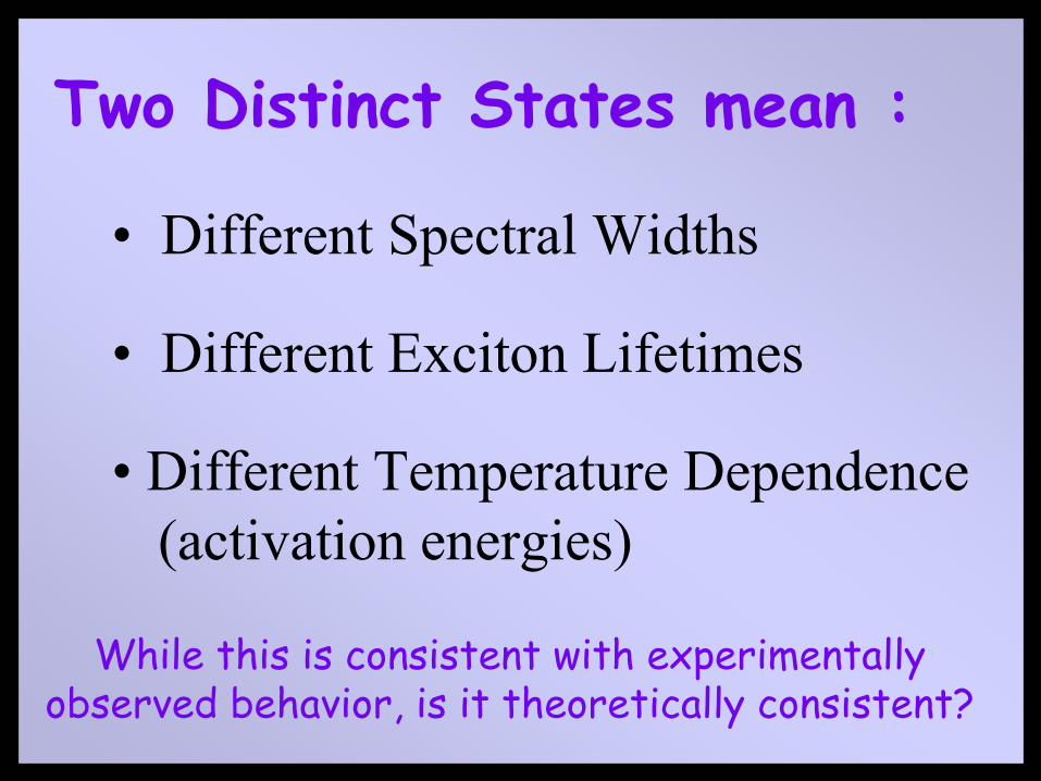
Two Distinct States mean :
• Different Spectral Widths
• Different Exciton Lifetimes
• Different Temperature Dependence (activation energies)
While this is consistent with experimentally observed behavior, is it theoretically consistent?
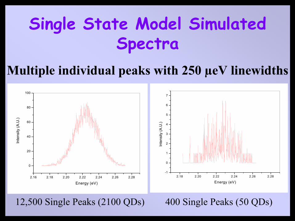
Single State Model Simulated Spectra
Multiple individual peaks with 250 µeV linewidths
2.16 2.18 2.20 2.22 2.24 2.26 2.28
0
20
40
60
80
100
Inte
nsity
(A.U
.)
Energy (eV)
2.18 2.20 2.22 2.24 2.26 2.28-1
0
1
2
3
4
5
6
7
Inte
nsity
(A.U
.)
Energy (eV)
12,500 Single Peaks (2100 QDs) 400 Single Peaks (50 QDs)
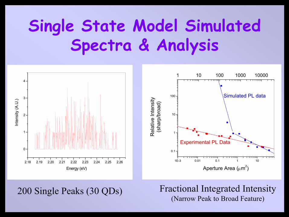
Single State Model Simulated Spectra & Analysis
2.18 2.19 2.20 2.21 2.22 2.23 2.24 2.25 2.26
0
1
2
3
4
Inte
nsity
(A.U
.)
Energy (eV)
1E-3 0.01 0.1 1 10
0.1
1
10
100
Experimental PL Data
Simulated PL data
Rel
ativ
e In
tens
ity(s
harp
/bro
ad)
Aperture Area (µm2)
1 10 100 1000 10000
Fractional Integrated Intensity(Narrow Peak to Broad Feature)
200 Single Peaks (30 QDs)
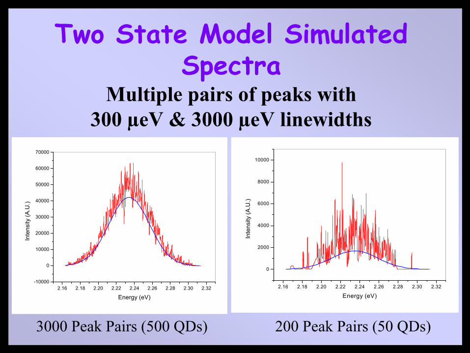
Two State Model Simulated Spectra
Multiple pairs of peaks with 300 µeV & 3000 µeV linewidths
2.16 2.18 2.20 2.22 2.24 2.26 2.28 2.30 2.32-10000
0
10000
20000
30000
40000
50000
60000
70000
Inte
nsity
(A.U
.)
Energy (eV)
2.16 2.18 2.20 2.22 2.24 2.26 2.28 2.30 2.32
0
2000
4000
6000
8000
10000
Inte
nsity
(A.U
.)
Energy (eV)
3000 Peak Pairs (500 QDs) 200 Peak Pairs (50 QDs)
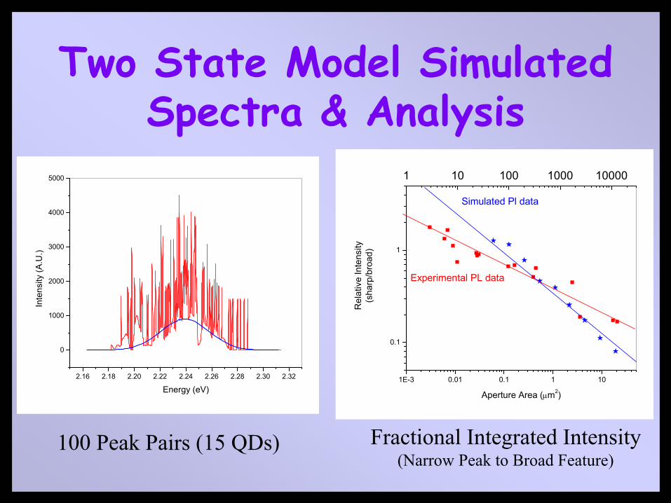
2.16 2.18 2.20 2.22 2.24 2.26 2.28 2.30 2.32
0
1000
2000
3000
4000
5000
Inte
nsity
(A.U
.)
Energy (eV)1E-3 0.01 0.1 1 10
0.1
1
Experimental PL data
Simulated Pl data
Rel
ativ
e In
tens
ity(s
harp
/bro
ad)
Aperture Area (µm2)
1 10 100 1000 10000
Fractional Integrated Intensity(Narrow Peak to Broad Feature)
Two State Model Simulated Spectra & Analysis
100 Peak Pairs (15 QDs)
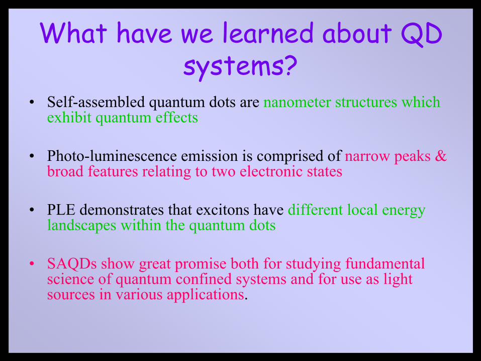
What have we learned about QD systems?
• Self-assembled quantum dots are nanometer structures which exhibit quantum effects
• Photo-luminescence emission is comprised of narrow peaks & broad features relating to two electronic states
• PLE demonstrates that excitons have different local energy landscapes within the quantum dots
• SAQDs show great promise both for studying fundamental science of quantum confined systems and for use as light sources in various applications.
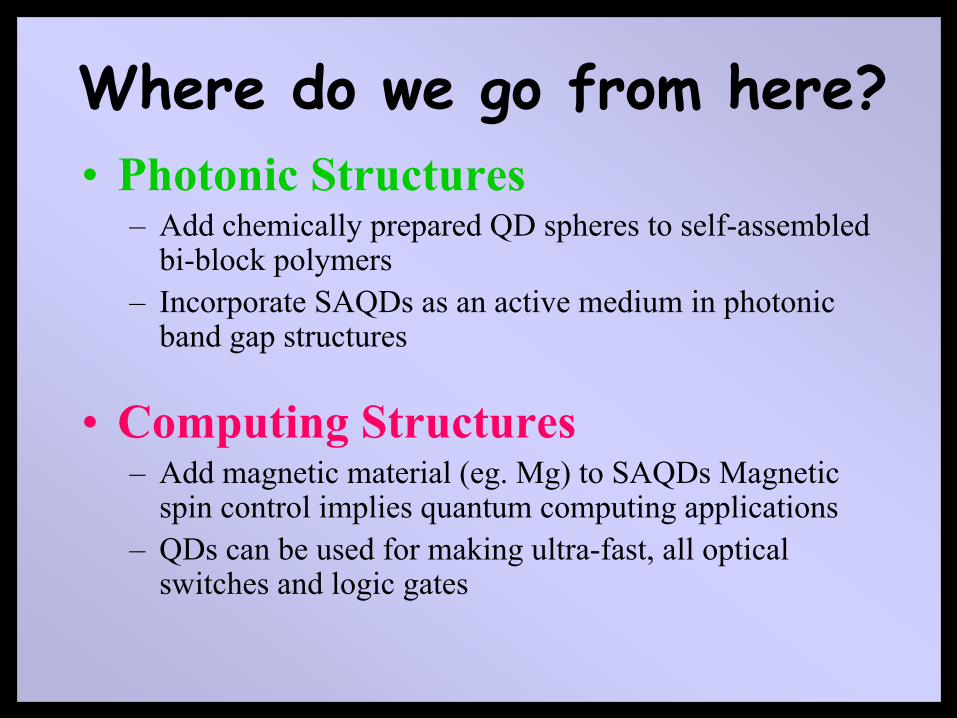
Where do we go from here?• Photonic Structures
– Add chemically prepared QD spheres to self-assembled bi-block polymers
– Incorporate SAQDs as an active medium in photonic band gap structures
• Computing Structures– Add magnetic material (eg. Mg) to SAQDs Magnetic
spin control implies quantum computing applications– QDs can be used for making ultra-fast, all optical
switches and logic gates
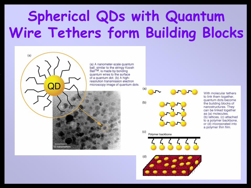
Spherical QDs with QuantumWire Tethers form Building Blocks
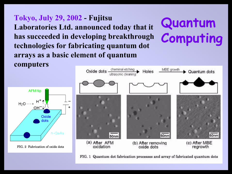
Tokyo, July 29, 2002 - Fujitsu Laboratories Ltd. announced today that it has succeeded in developing breakthrough technologies for fabricating quantum dot arrays as a basic element of quantum computers
Quantum Computing
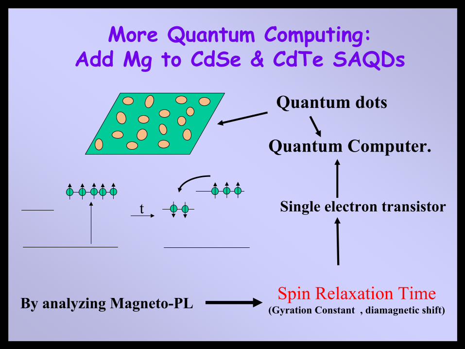
More Quantum Computing:Add Mg to CdSe & CdTe SAQDs
Quantum dots
By analyzing Magneto-PL Spin Relaxation Time(Gyration Constant , diamagnetic shift)
Quantum Computer.
Single electron transistort
"The National Nanotechnology Initiative is a big step in a vitally important direction. It will send a clear signal to the youth of this country that the hard core of physical science (particularly physics and chemistry) and the nanofrontiersof engineering have a rich, rewarding future of great social relevance. The coming high tech of building practical things at the ultimate level of finesse, precise right down to the lastatom, has the potential to transform our lives. Physics and chemistry are the principal disciplines that will make this all happen. But they are hard disciplines to master, and far too few have perceived the rewards at the end of the road sufficient to justify the effort. The proposed NNI will help immensely to inspire our youth.“
Richard E. SmalleyGene and Norman Hackerman Professor of Chemistry and Professor of PhysicsRice University Center for Nanoscale Science and Technology
Conclusion

Quantum Dots:A Physicist’s (& Chemist’s)
Playground
Jan Yarrison-Rice, Physics Dept.Miami University
2 .1 6 2 .1 8 2 .2 0 2 .2 2 2 .24 2 .26 2 .2 8 2 .3 0 2 .3 2
0
1 0 00
2 0 00
3 0 00
4 0 00
5 0 00
Inte
nsity
(A.U
)
E n e rg y (e V )