Embed Size (px)
Citation preview
SILICON NANODEVICE QUBITS BASED ON
QUANTUM DOTS AND DOPANTS
ANASUA CHATTERJEE
SUBMITTED IN PARTIAL FULFILMENT OF
THE REQUIREMENTS FOR THE DEGREE OF
DOCTOR OF PHILOSOPHY
DEPARTMENT OF PHYSICS AND ASTRONOMY
UNIVERSITY COLLEGE LONDON
JANUARY 2017

c© Copyright Anasua Chatterjee, 2017.
All rights reserved.
I, Anasua Chatterjee, confirm that the work presented in this thesis is my own. Where
information has been derived from other sources, I confirm that this has been indicated in
the thesis.
Anasua Chatterjee

Abstract
Silicon Nanodevice Qubits Based on Quantum Dots and Dopants
Anasua Chatterjee
Quantum physics applied to computing is predicted to lead to revolutionary enhancements
in computational speed and power. The interest in the implementation of an impurity spin
based qubit in silicon for quantum computation is motivated by exceedingly long coher-
ence times of the order of seconds, an advantage of silicon’s low spin orbit coupling and
its ability to be isotopically enriched to the nuclear spin zero form. In addition, the donor
spin in silicon is tunable, its nuclear spin is available to be employed as a quantum mem-
ory, and there are major advantages to working with silicon in terms of infrastructure and
scalability. In contrast, lithographically patterned artificial atoms called quantum dots have
the complementary advantages of fast electrical operations and tunability.
Here I present our attempts to develop a scalable quantum computation architecture in
silicon, based on a coupled quantum dot and dopant system. I explore industry-compatible
as well as industrial foundry-fabricated devices in silicon as hosts for few-electron quan-
tum dots and utilise a high-sensitivity readout and charge sensing technique, gate-based
radiofrequency reflectometry, for this purpose. I show few-electron quantum dot mea-
surements in this device architecture, leading to a charge qubit with a novel multi-regime
Landau-Zener interferometry signature, with possible applications for readout sensitivity. I
also present spin-to-charge conversion measurements of a chalcogen donor atom in silicon.
Lastly, I perform measurements on a foundry-fabricated silicon device showing a coupling
between a donor atom and a quantum dot. I probe the relevant charge dynamics of the
charge qubit, as well as observe Pauli spin blockade in the hybrid spin system, opening up
the possibility to operate this coupled double quantum dot as a singlet-triplet qubit or to
transfer a coherent spin state between the quantum dot and the donor electron and nucleus.
5

Acknowledgements
It is a truth universally acknowledged, that a graduate student in possession of a finished
thesis must have a large number of people to thank. First on that very long list would be
my advisor John, who has been extremely supportive, and very patient about my many
non-traditional1 ideas and plans. His understanding, tolerance for stupid questions and
late-night panicky emails2 and calm demeanour mean that I always regain some perspec-
tive after a meeting with him. His remarkable and wide ranging scientific knowledge and
intuition, as well as his dedication to forming and maintaining fruitful collaborations has
given me so much to learn from.
The London lab gang have been sources of commiseration, empathy and a lot of laugh-
ter over these years. Cheuk, one of the first people I met when I arrived, has been a rock of
support through all my experiments, and the horrors of silicon device fabrication (where his
knowledge is unparalleled, as is his uncannily steady hand with tweezers). Matias, the other
half of the fridge duo, has taught me so much about low-noise cryogenic measurement3,
as well as the importance of keeping calm (it helps if you whistle, however annoyingly),
cultivating healthy detachment (I think it’s safe to say I’ve failed at this), and reading the
arXiv everyday. Jarryd set high standards for everything in the lab, while Gary and Roberto
were very patient with someone who’d never even seen a spectrometer before. In the small
amount of time I had with Vasileia, Stephanie and Richard, I received a lot of advice and
help from them and I wish them the best. Naitik and Philipp have been great friends despite
my constant whining to them, while John Mansir and Simon will be worthy successors to
Bender the fridge. Salahuddin’s antics bring some much needed laughter to the lab, and
Eva, with her readiness to help with matters scientific and otherwise, will be greatly missed,
1British for “crazy”. In the same vein, “very interesting” is likely to mean “that is utter nonsense”, and“minor comments” indicates you need to rewrite everything.
2and being almost murdered on a ski slope by a flailing beginner...3Also that you need to microwave flaming shots before you set them on fire...not in the lab of course!
7
as will the F10 lab itself (though not the treacherous pipes). Christoph and HeeJin haven’t
yet learnt that as postdocs they should be ordering us around, and spend their time helping
us instead; don’t change, guys! To the new cohort (Simon, James, Gavin, Pierandrea and
David): may the little blue minifridge never be empty (though chartreuse is clearly superior
to beer).
I’ve been fortunate enough to be a part of the London Centre for Nanotechnology,
which I have seen go from strength to strength over these four years. My colleagues at the
LCN have all fostered an atmosphere of collaboration and scientific inquiry; I would like
to thank especially Mark Buitelaar, my second supervisor, for his support and expertise,
Jeroen Elzerman, Jonathan Burnett (and everyone from Warburton group) and especially
Andrew Fisher for his unstinting mentorship and willingness to listen to researchers.
To the Cambridge crowd, thanks for putting up with me for six whole months; I really
enjoyed my time at the Cavendish (some of it due to the excellent coffee machine!). In par-
ticular, Fernando’s depth of knowledge about reflectometry has been extremely educational
for me, and I have benefited from his strong support and thoroughness in all matters sci-
entific4. Nick’s depth of knowledge about microwave engineering and most things physics
is almost frightening; though he is the exact opposite as a landlord5. Andrew Ferguson,
Alessandro Rossi, Andi Betz, Adam Esmael, James Haigh, have all made my stay at Cam-
bridge fruitful and fun. At Southampton, Feras and now Liam have kept the silicon MOS
flag flying high, and it’s great to see devices result from all our collective hard work. In my
month and a half at Copenhagen I have experienced a wonderfully well-run lab where it is
such a pleasure to do science6, and I have to thank Charlie and Ferdinand for welcoming
me and giving me free rein on a precious dilution fridge, as well as Christian, Filip, and
4and culinary; “chorizo in everything...but never in paella!”5written in expectation of more excellent baked goods6the fact that it is the first lab I’ve worked in that isn’t dark and underground also helps, as does the
glorious coffee machine!
8
Frederico for their help and companionship. Karl, whom I seem to be following around the
world, has been as helpful as he was in Princeton, and remains scarily efficient as always.
Pettalab (and of course Princeton itself) has had a great hand in making me the researcher
I am, and I’d like to thank my first advisor Jason Petta, who continues to be a true mentor
and friend, and who set me on the path to a PhD in experimental condensed matter when I
was a young undergraduate susceptible to the charms of theoretical physics. Lastly, I’d like
to thank CEA-LETI for the excellent devices they made for us, and continue to make.
For feeding and housing me in the expensive sinkhole for money that is London7, I
would like to thank the EPSRC, as well as the UCL Dean’s Prize, the UNDEDD grant, and
the Yusuf Ali travel grant.
I’d like to thank my huge rambunctious family who are a welcome relief from the
academic bubble and a reality check that good things exist outside the lab. Their support
and love has been unconditional and plentiful, even during the times when I disappear
into experiments and forget to call (or treat vacations like writing retreats). To my father
who gave me the Feynman lectures when I was way too young and kickstarted this whole
painful process, I say a grudging but heartfelt thank you. I thank my mother for always
unconditionally taking my side whenever I vent to her; and yes I do like physics more than
biology (her subject).
Lastly, to the long-suffering Sroyon, who has made these four years the happiest in
my life, thank you so much. For following me around to different cities at the drop of a
hat, for putting up with my worst-case scenarios and long absences in the lab, quelling my
late-night panic attacks (“yes I’m sure you turned off that one valve”), and for generally
looking at the world with eternal surprise.
7though I would like to thank the city for its excellent 24-hour night buses that have saved my life aftermany a late night in the lab
9

To my dadu, who taught a little girl to read.
10
Contents
Abstract . . . . . . . . . . . . . . . . . . . . . . . . . . . . . . . . . . . . . . . 5Acknowledgements . . . . . . . . . . . . . . . . . . . . . . . . . . . . . . . . . 7List of Tables . . . . . . . . . . . . . . . . . . . . . . . . . . . . . . . . . . . . 13List of Figures . . . . . . . . . . . . . . . . . . . . . . . . . . . . . . . . . . . . 14
1 Background and Motivation 171.1 Silicon spin qubits for quantum computation . . . . . . . . . . . . . . . . . 181.2 Donor spins in silicon . . . . . . . . . . . . . . . . . . . . . . . . . . . . . 191.3 Quantum dots in semiconductors . . . . . . . . . . . . . . . . . . . . . . . 221.4 The dopant-dot hybrid qubit . . . . . . . . . . . . . . . . . . . . . . . . . 221.5 Thesis outline . . . . . . . . . . . . . . . . . . . . . . . . . . . . . . . . . 24
2 Quantum Dots 272.1 Single and double quantum dot devices . . . . . . . . . . . . . . . . . . . 272.2 Coulomb blockade and charge sensing . . . . . . . . . . . . . . . . . . . . 292.3 Charge qubits . . . . . . . . . . . . . . . . . . . . . . . . . . . . . . . . . 342.4 Landau-Zener interferometry . . . . . . . . . . . . . . . . . . . . . . . . . 362.5 Spin qubits and Pauli spin blockade . . . . . . . . . . . . . . . . . . . . . 432.6 Dopant spins in silicon . . . . . . . . . . . . . . . . . . . . . . . . . . . . 49
3 Experimental Techniques 553.1 Electrically Detected Magnetic Resonance . . . . . . . . . . . . . . . . . . 553.2 Measurement setup and techniques . . . . . . . . . . . . . . . . . . . . . . 583.3 Gate-based RF-reflectometry . . . . . . . . . . . . . . . . . . . . . . . . . 633.4 Fabrication of nanoscale silicon devices . . . . . . . . . . . . . . . . . . . 683.5 CMOS foundry silicon-on-insulator devices . . . . . . . . . . . . . . . . . 77
11
4 Gate-based charge sensing of a double quantum dot in a silicon nanowire 824.1 Primary thermometry . . . . . . . . . . . . . . . . . . . . . . . . . . . . . 844.2 Microwave sensing . . . . . . . . . . . . . . . . . . . . . . . . . . . . . . 924.3 Multi-regime Landau-Zener Stuckelberg interferometry in a double quan-
tum dot . . . . . . . . . . . . . . . . . . . . . . . . . . . . . . . . . . . . 954.4 LZS results and discussion . . . . . . . . . . . . . . . . . . . . . . . . . . 1014.5 Theoretical description . . . . . . . . . . . . . . . . . . . . . . . . . . . . 1064.6 Outlook and conclusion . . . . . . . . . . . . . . . . . . . . . . . . . . . . 113
5 Electrically Detected Magnetic Resonance of Selenium Donors in Silicon 1155.1 Introduction: deep double donors in silicon . . . . . . . . . . . . . . . . . 1155.2 Sample design and measurement Setup . . . . . . . . . . . . . . . . . . . . 1265.3 EDMR spectrum . . . . . . . . . . . . . . . . . . . . . . . . . . . . . . . 1295.4 Temperature and power dependence of the EDMR signal . . . . . . . . . . 1305.5 Effects of laser and broad-wavelength illumination . . . . . . . . . . . . . 1365.6 Analysis . . . . . . . . . . . . . . . . . . . . . . . . . . . . . . . . . . . . 139
6 A Hybrid Dopant-Dot Double Quantum Dot in Silicon 1496.1 Device and measurement setup . . . . . . . . . . . . . . . . . . . . . . . . 1506.2 Double quantum dot behaviour . . . . . . . . . . . . . . . . . . . . . . . . 1506.3 Microwave spectroscopy . . . . . . . . . . . . . . . . . . . . . . . . . . . 1556.4 Charge relaxation . . . . . . . . . . . . . . . . . . . . . . . . . . . . . . . 1586.5 Spin blockade . . . . . . . . . . . . . . . . . . . . . . . . . . . . . . . . . 1616.6 Conclusions . . . . . . . . . . . . . . . . . . . . . . . . . . . . . . . . . . 1636.7 Methods for coherent control . . . . . . . . . . . . . . . . . . . . . . . . . 164
7 Conclusion and Outlook 1687.1 Outlook and future work . . . . . . . . . . . . . . . . . . . . . . . . . . . 172
A Fabrication Listings 175
B Measurement Notes 181
Bibliography 191
12
List of Tables
3.1 Test structures for the silicon fabrication platform . . . . . . . . . . . . . . 75
5.1 Experimental values for donors in silicon . . . . . . . . . . . . . . . . . . 120
A.1 Silicon MOS fabrication process flow . . . . . . . . . . . . . . . . . . . . 175A.2 CEA-Leti die, postprocessing and stripline fabrication . . . . . . . . . . . . 178A.3 EDMR interdigitated contact fabrication . . . . . . . . . . . . . . . . . . . 180
13
List of Figures
1.1 Device implementations of donor, quantum dot, and coupled systems . . . . 21
2.1 Device implementations of quantum dot systems . . . . . . . . . . . . . . 282.2 Transport through a single quantum dot . . . . . . . . . . . . . . . . . . . 312.3 Double quantum dots and the stability diagram . . . . . . . . . . . . . . . 332.4 Triple points in double quantum dot transport . . . . . . . . . . . . . . . . 352.5 A tunnel coupled charge qubit . . . . . . . . . . . . . . . . . . . . . . . . 362.6 Evolution of the energies during Landau-Zener interferometry . . . . . . . 372.7 Charge qubit manipulation through Landau-Zener Interferometry . . . . . . 402.8 Effect of decoherence on the Landau-Zener interferometry pattern . . . . . 422.9 Spin blockade in quantum dot systems . . . . . . . . . . . . . . . . . . . . 432.10 Spin qubit manipulation . . . . . . . . . . . . . . . . . . . . . . . . . . . . 462.11 Donor wavefunction in silicon . . . . . . . . . . . . . . . . . . . . . . . . 502.12 Breit-Rabi diagrams of donors . . . . . . . . . . . . . . . . . . . . . . . . 53
3.1 ESR and EDMR setup . . . . . . . . . . . . . . . . . . . . . . . . . . . . 573.2 DC line anchoring and filtering . . . . . . . . . . . . . . . . . . . . . . . . 603.3 On-PCB copper powder and RC filtering . . . . . . . . . . . . . . . . . . . 613.4 Fridge printed circuit board . . . . . . . . . . . . . . . . . . . . . . . . . . 633.5 RF reflectometry setup . . . . . . . . . . . . . . . . . . . . . . . . . . . . 643.6 RF-resonance from a loaded tank circuit . . . . . . . . . . . . . . . . . . . 653.7 Regimes of gate-based reflectometry . . . . . . . . . . . . . . . . . . . . . 663.8 Silicon device fabrication platform . . . . . . . . . . . . . . . . . . . . . . 703.9 The stages of Metal-Oxide-Semiconductor lithography. . . . . . . . . . . . 713.10 Fabricated devices . . . . . . . . . . . . . . . . . . . . . . . . . . . . . . . 733.11 Device tests and design progression . . . . . . . . . . . . . . . . . . . . . 783.12 Foundry-fabricated FD-SOI devices . . . . . . . . . . . . . . . . . . . . . 80
14
4.1 Gate-based reflectometry of a quantum dot . . . . . . . . . . . . . . . . . . 854.2 Device and reflectometry setup . . . . . . . . . . . . . . . . . . . . . . . . 874.3 Peak shape, FWHM and amplitude with mixing chamber temperature . . . 914.4 RF-drive broadening and gate lever arm . . . . . . . . . . . . . . . . . . . 934.5 Microwave effects and simulations . . . . . . . . . . . . . . . . . . . . . . 964.6 Stability diagram in transport and reflectometry . . . . . . . . . . . . . . . 1004.7 Phase response of the resonator under Landau-Zener interferometry . . . . 1024.8 Frequency dependence of the LZS interferometry pattern . . . . . . . . . . 1054.9 Circuit model, stability diagram and energy levels of the double quantum dot1074.10 Multiple-passage regime . . . . . . . . . . . . . . . . . . . . . . . . . . . 1094.11 Single-passage regime . . . . . . . . . . . . . . . . . . . . . . . . . . . . 1104.12 Double-passage regime . . . . . . . . . . . . . . . . . . . . . . . . . . . . 1114.13 Landau-Zener interferometry in a four-level system . . . . . . . . . . . . . 112
5.1 Shallow and deep donors in silicon . . . . . . . . . . . . . . . . . . . . . . 1175.2 Selenium hyperfine transitions . . . . . . . . . . . . . . . . . . . . . . . . 1195.3 Ionization energies and donor species populations with temperature . . . . 1215.4 EDMR sample and measurement setup . . . . . . . . . . . . . . . . . . . . 1265.5 EDMR spectrum of 28-Si:77Se device . . . . . . . . . . . . . . . . . . . . 1305.6 Power dependence of EDMR and ESR signals . . . . . . . . . . . . . . . . 1325.7 Peak-to-peak linewidth . . . . . . . . . . . . . . . . . . . . . . . . . . . . 1345.8 Temperature dependence of the EDMR Signal . . . . . . . . . . . . . . . . 1355.9 Modulation frequency . . . . . . . . . . . . . . . . . . . . . . . . . . . . . 1365.10 Effect of white light and laser illumination . . . . . . . . . . . . . . . . . . 1375.11 Change in photocurrent at resonance . . . . . . . . . . . . . . . . . . . . . 1385.12 Spin dependent recombination . . . . . . . . . . . . . . . . . . . . . . . . 142
6.1 Dopant-dot device and setup . . . . . . . . . . . . . . . . . . . . . . . . . 1516.2 Double dot stability diagram . . . . . . . . . . . . . . . . . . . . . . . . . 1526.3 Charge assignment of dopant and dot transitions . . . . . . . . . . . . . . . 1536.4 Magnetic field dependence of donor transition . . . . . . . . . . . . . . . . 1546.5 The dopant-dot hybrid system . . . . . . . . . . . . . . . . . . . . . . . . 1556.6 Microwave spectroscopy . . . . . . . . . . . . . . . . . . . . . . . . . . . 1576.7 Charge relaxation measurement protocol . . . . . . . . . . . . . . . . . . . 1596.8 Charge relaxation time . . . . . . . . . . . . . . . . . . . . . . . . . . . . 160
15
16
6.9 Pauli Spin Blockade . . . . . . . . . . . . . . . . . . . . . . . . . . . . . . 1626.10 Electron Spin Resonance . . . . . . . . . . . . . . . . . . . . . . . . . . . 1656.11 Coplanar Waveguide for ESR measurements . . . . . . . . . . . . . . . . . 166
7.1 Qubit configurations for silicon nanowire finFETs . . . . . . . . . . . . . . 170
A.1 EDMR spectrum prior to surface treatment . . . . . . . . . . . . . . . . . . 180
B.1 Room temperature RF setup . . . . . . . . . . . . . . . . . . . . . . . . . 183B.2 Additional dopant-dot device measurements . . . . . . . . . . . . . . . . . 186B.3 Microwave simulations for a dot-to-lead transition . . . . . . . . . . . . . . 187B.4 Coplanar waveguide model . . . . . . . . . . . . . . . . . . . . . . . . . . 190
Chapter 1
Background and Motivation
Quantum physics, when applied to computing, is projected to lead to revolutionary en-hancements in computational speed and power. This thesis focuses on quantum informationand quantum computing, specifically through quantum architectures built from hybrid sys-tems, which can couple distinct qubit implementations with complementary advantages.In traditional computing, “Moore’s law” observes that the number of FETs (field effecttransistors) on an integrated circuit doubles approximately every two years to enable tra-ditional semiconductor-based computing systems to grow in speed and processing power.However, we appear close to a limit to Moore’s Law, since MOSFETs are reaching a phys-ical scalability limit[1] in the sense that they cannot be made much smaller, or be packedin much more densely. However, quantum computing is projected to bring as regime-changing an upheaval as the first transistor, with exponential speedups in many processessuch as codebreaking[2] and quantum simulation[3] that are just too computationally in-tensive today.
There are indeed challenges commensurate to these rewards. The building blocks ofsuch a quantum computer, called qubits, have to be resistant to environmental disturbance;they need to hold information encoded in them for long periods as well as be easy tocontrol. This is unfortunate, since often these two qualities are somewhat antithetical;if something is easy to interact with and control, this often means that the environmentis also able to interact with it in ways that affect the coherence of information stored init. As a result quantum physicists are increasingly looking towards hybrid systems today.Combining a system with high resistance to environmental interference with one that iseasier to control and engineer is a promising approach for building an effective quantumcomputing architecture. This work seeks to explore just such a novel, hybrid building
17
CHAPTER 1. BACKGROUND AND MOTIVATION 18
block; the quantum dot coupled to an impurity spin in silicon. In doing so, we also aim togain understanding into the physical system composed of a natural atom (the dopant atomin the silicon crystal) coupled to an artificial atom (the gate-defined quantum dot).
1.1 Silicon spin qubits for quantum computation
Silicon, as the material of choice of the semiconductor industry, is ubiquitous in hardwarefor classical computation and consequently in all our consumer electronic devices. It turnsout that silicon also has quite a few advantages over other materials as a quantum com-puting platform as well, which we can evaluate in terms of the DiVincenzo criteria[4], aset of five requirements for qubits suitable for quantum computation. These can be brieflysummarised as: the qubit must be scalable and well characterised, it must be able to be ini-tialised, as well as manipulated, by a universal set of quantum gates, it must not decoherequickly, and it should be able to be read out with high fidelity. Any quantum technol-ogy built on silicon is inherently more scalable, having the semiconductor industry and itsfabrication skill and technology to draw upon. Silicon is also an excellent semiconductorvacuum for spin (i.e. a low magnetic-decoherence causing environment), containing onlya very few decoherence centers in the form of the (spin-1/2) 29Si isotope, so that qubitsin silicon are protected from many sources of noise that decohere other qubits. Moreover,silicon can be isotopically purified to the (spin-0) 28Si isotope, giving extraordinary gainsin the coherence of stored quantum information. In terms of the DiVincenzo criteria, weare now left with the requirements of initialisation, manipulation and high-fidelity readout,which we explore in the next section (and in the rest of this thesis).
1.1.1 The semiconductor industry
Our interest in silicon provides a secondary motivation for the experiments performed inthis thesis. In its quest for faster and more powerful computers, the semiconductor industryhas strongly embraced miniaturization. However as we have discussed, this scaling downprocess has a limit and we are indeed now very near it; around a gate length of∼5 nm. Theproximity of the source and drain electrodes can now lead to short-channel effects such aspunch through and atomistic variations across chips. However, while this is a problem forthe semiconductor industry, it provides a motivation for the disruptive technology that isquantum computation. In addition it is worth underlining that this process of miniaturiza-
CHAPTER 1. BACKGROUND AND MOTIVATION 19
tion also provides us with a resource that this thesis aims to take advantage of; high qualityfew-nm sized devices, produced with great reliability in ultra-clean environments with in-tegrated control electronics, which are capable of harbouring both few electron quantumdots and dopant atoms and therefore a hybrid system. Through the experiments performedin this thesis, we have tried to develop a silicon architecture that is truly compatible withthe silicon industry, by exploring quantum dot behaviour that is well-explained by theory,but established in large-scale foundry-made devices.
1.2 Donor spins in silicon
Silicon is a mainstay of the electronics industry, but along with it are impurity atoms calleddopants embedded in the crystal lattice which are essential for microelectronics. Of these,“donors” are atoms with an extra electron to donate to the semiconductor, typically fromGroup V (P, As, Sb, or Bi) in the periodic table, occupying substitution sites in the sil-icon lattice. These are typically “shallow” donors, with the single electron ground state∼ 50 meV below the conduction band edge (though we will explore a “deep” donor, fromGroup VI, in a later chapter). At low temperatures (< 50 K) these atoms have a boundelectron and a nucleus, both of which have a spin degree of freedom that can be probed andmanipulated using established methods such as Electron Spin Resonance (ESR).
1.2.1 State of the art for donor qubits in silicon
Research in the field of dopant atoms in semiconductor materials has been conducted formore than fifty years, well before the conception of quantum information. In 1998, how-ever, interest in these donors as the physical implementations of qubits took off with thepublication of the Kane proposal[5], which proposed a computer consisting of arrays ofqubits made up of the spin state of donor nuclei. Below are some developments in donorspin qubits that contribute to the realisation of a Kane computer:
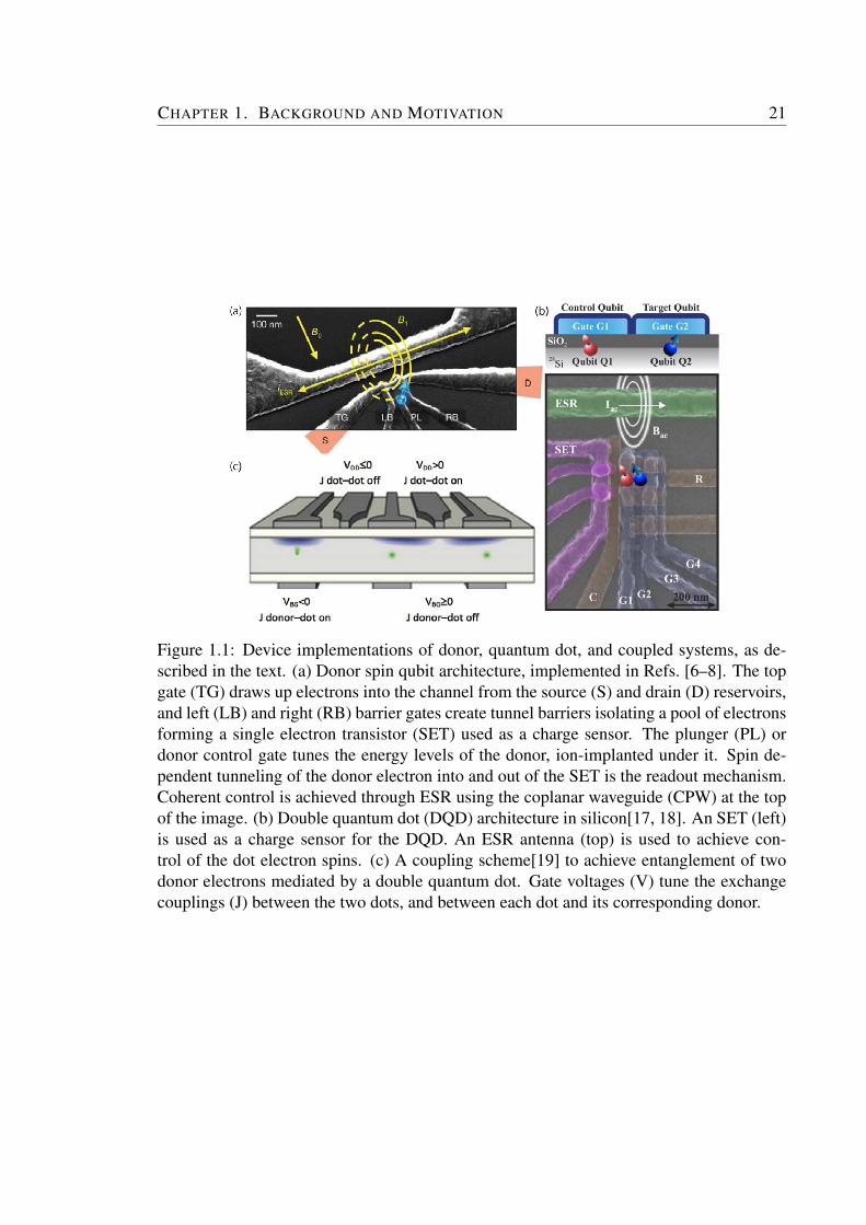
• Readout and control of donor spins The reading out of the spin state of the qubit isan extremely important first step. In 2010, the single-shot readout of the electron spinof a phosphorus atom in silicon using spin-to-charge conversion was reported[6].This readout method was then combined with coherent control to achieve a singlespin-qubit in silicon[7] with a coherence time of 200 µs (with an architecture shownin Fig. 1.1(a)). This was followed by the readout and control of a nuclear spin qubit in
CHAPTER 1. BACKGROUND AND MOTIVATION 20
silicon[8] with a coherence time of 60 ms. Soon after, a substrate with an isotopicallypurified Si-28 epilayer was used to replicate these results but with great gains incoherence times (30 s for the nuclear spin, and 0.5 s for the electron spin[9]), settinga benchmark for solid state qubits.
• Donor placement The Kane computer requires near-atomic precision of donorplacement in the silicon lattice, about 10 nm apart. Ion implantation[7, 8, 10] usinglithographically opened windows as well as scanning probe microscopy[11] methodshave been employed for this purpose. The latter provides the near-atomic precisionrequired for the Kane proposal.
• Spin-selective addressing Electron spin resonance (ESR) manipulation is usuallyused to control donor spins; however this is typically a global method, and the Kaneproposal requires a way of addressing individual spins. The Stark shift using elec-tric tuning through gate voltages has been proposed for this purpose and has beendemonstrated in ensembles of donors[12, 13], as well as recently in devices[14].
• Two-qubit gates and the nuclear spin Single and two-qubit gates form a universalset of quantum gates, required for any quantum computer. Kane’s original proposalenvisaged using controllable electron-mediated exchange coupling between adjacentnuclear spins, requiring fine control over the inter-electron wavefunction overlap.This is difficult to engineer over any large distance, and also in part because of os-cillations in the exchange due to interference in the electron wavefunction by thesix-fold degenerate conduction band minima of silicon[15]. In general, the couplingand interaction of neighbouring nuclear spins is quite a difficult question for a donor-based quantum computer, a challenge recognised in Kane’s original proposal. Whilethe donor electron’s spin is easier to address (and the coherent transfer of a quantumstate between the electron and nuclear spin has been demonstrated[16]), this is alsonot trivial.
From the above discussion, there emerges a need for a fast method of manipulation thatwill enable us to entangle nearby donor electron or nuclear spins. Additionally, donors insilicon also have the drawback of being low in tunability compared to artificial atoms, inparticular the electrostatically defined quantum dot.
CHAPTER 1. BACKGROUND AND MOTIVATION 21
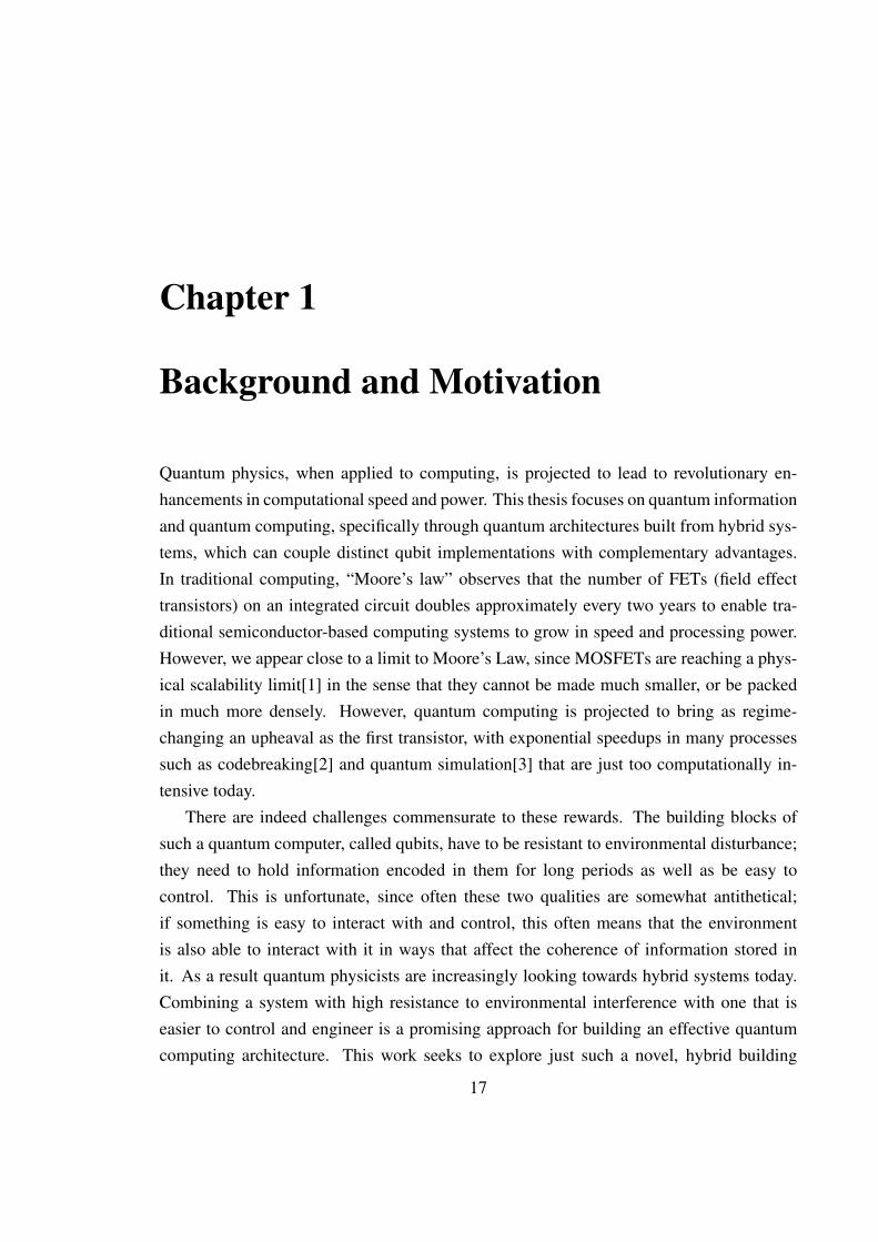
Figure 1.1: Device implementations of donor, quantum dot, and coupled systems, as de-scribed in the text. (a) Donor spin qubit architecture, implemented in Refs. [6–8]. The topgate (TG) draws up electrons into the channel from the source (S) and drain (D) reservoirs,and left (LB) and right (RB) barrier gates create tunnel barriers isolating a pool of electronsforming a single electron transistor (SET) used as a charge sensor. The plunger (PL) ordonor control gate tunes the energy levels of the donor, ion-implanted under it. Spin de-pendent tunneling of the donor electron into and out of the SET is the readout mechanism.Coherent control is achieved through ESR using the coplanar waveguide (CPW) at the topof the image. (b) Double quantum dot (DQD) architecture in silicon[17, 18]. An SET (left)is used as a charge sensor for the DQD. An ESR antenna (top) is used to achieve con-trol of the dot electron spins. (c) A coupling scheme[19] to achieve entanglement of twodonor electrons mediated by a double quantum dot. Gate voltages (V) tune the exchangecouplings (J) between the two dots, and between each dot and its corresponding donor.
CHAPTER 1. BACKGROUND AND MOTIVATION 22
1.3 Quantum dots in semiconductors
In the same year as the Kane proposal, Loss and DiVincenzo[20], proposed another kind ofqubit, the quantum dot. Semiconductor quantum dots are typically gate-confined regions ofa substrate, typically tens of nanometers in size, which can be used to form potential wellsin which to trap electrons and form artificial atoms with discrete, quantized energy lev-els. The quantum dot as a qubit has providentially complementary attributes to the donoratom; potentially not as long-lived, but comparatively easy to engineer as well as tune.These qubits also provide fast control of spin states through electrical voltages (which aremuch easier to apply, especially locally, than magnetic fields). They are able to be fabri-cated using silicon as the substrate, a material which can also host our donor atoms for ahybrid architecture. In terms of scalability, arrays of quantum dots are also easier to fab-ricate than those of donors, since this typically involves a repeating lithography pattern,whereas for single donors, precise single-ion implantation techniques are required. In sil-icon (more specifically, in a SiGe heterostructure), a linear array of 9 quantum dots wasrecently implemented[21]. In Chapter 2 we present in detail the background, theory andmeasurement of semiconductor quantum dots, with particular emphasis on silicon.
Fig. 1.1(b) shows an architecture in silicon recently used to isolate a double quantumdot (the high degree of control available through precisely engineered overlapping gatesis notable). Quantum dots patterned on silicon in general have shorter coherence timesthan donor atoms; recent experiments[17] on a device based on a silicon substrate with anisotopically purified 28Si epilayer have found a coherence time of T2 ∼28 ms (a value mea-sured using the CPMG pulse sequence; using the same sequence, T2 ∼ 560 ms was foundfor a donor electron spin and T2 ∼ 35.6 s for an ionised donor nuclear spin[9]). However,in this quantum dot device, one-qubit gates and the recently demonstrated two-qubit gates(essential operational steps for the implementation of universal quantum computation) canbe performed in a time that allows for 105 two-qubit gates within one T2[18]. This fastoperation time is what makes these quantum dots attractive as computational units.
1.4 The dopant-dot hybrid qubit
An apparent next step would be to harness the complementary advantages of these twosystems, by placing them in close proximity and coupling them together to exchange infor-mation. This thesis explores ways in which this kind of coupling can be achieved, as well
CHAPTER 1. BACKGROUND AND MOTIVATION 23
as tries to find optimum dopant and dot systems for which this can be implemented. Weare also interested in implementing this dopant-dot coupling in a scalable silicon devicearchitecture. A hybrid architecture with a quantum dot coupled to a donor atom, forminga novel kind of double quantum dot could take advantage of fast spin manipulations usinggate voltages to form a hybrid singlet-triplet qubit. The system would also have access tothe long-lived quantum memory offered by the nuclear spin of the donor atom, the naturalfield gradient from which could also be used to drive spin rotations. Another potential ap-plication could be the creation of spin buses with quantum dots chains to mediate quantuminformation stored in donor qubit over long distances[22]. Additionally, in a hybrid archi-tecture, entangled states could be operated upon in a double quantum dot, and could thenbe transferred to the long-lived nuclear spins of two donors, the memory element.
An important step is to achieve quantum state transfer between the donor and the dot.Two possible ways to achieve this are mentioned below.
Electron shuttling
One way of accomplishing the transfer of spin information is to physically transfer theelectron carrying the spin information from the dot to the dopant. To explore transfer of aquantum state, we start out with a lithographically defined double quantum dot (DQD) in atriplet ground state (at a small magnetic field), as well as a dopant in the positively chargedD+ state. By pulsing gate voltages, we can shuttle the electron from one of the quantumdots into the dopant, wait some time, and shuttle back into the QD. The probability ofthe singlet state (zero in the absence of any spin flips) will indicate if the electron can betransferred between the QD and dopant in a spin-conserving way. The singlet state can bemeasured using a quantum capacitance measurement[23] using gate based charge sensingor alternatively, a proximal RF-SET charge sensor. Coherent transfer by adiabatic passage(CTAP)[24, 25] has been suggested to achieve electron shuttling. However, the coherenttransfer of information by physically moving electrons is acknowledged to be difficult,though the physical shuttling of electrons across three quantum dots has been recentlyachieved[26].
Exchange coupling
A second perhaps more feasible method, aims to create a dopant-dot singlet triplet qubit,with greater tunability and spin coherence expected than in the shuttling approach since
CHAPTER 1. BACKGROUND AND MOTIVATION 24
there is no physical movement of the quantum systems. The essential ingredient is anexchange coupling (ideally electrostatically controlled) between one of the dots andthe dopant. Fig. 1.1(c) shows an architecture where electrostatically tunable exchangecouplings (“J dot-dot”, JDQD and “J donor-dot”, JDD) would facilitate a memory SWAPoperation[19]. A starting point would be a DQD in the (1,1) singlet state and a dopant inthe neutral D0 spin-down state, with the coupling JDD switched off. Then, with an appro-priately timed voltage pulse, JDD would be turned on to entangle the donor and quantumdot spins so that the DQD would have some probability of being in the triplet state. Varyingthe JDD pulse length would induce oscillations in the DQD triplet population, enabling ameasurement of the dopant-dot exchange coupling and operation of the hybrid system asa singlet-triplet qubit. When this is performed on both halves of the double quantum dotwith two singly-coupled donors, it would pass an entangled state from the DQD to the twodonor electron spins (which could then be extended to the even longer-lived donor nuclearspins).
In recent times, coupling of a dopant to a dot has been an area of focused research.Spectroscopy of dopant states in the coulomb blockade regime of a quantum dot has beenshown[27, 28]. In a silicon nanowire device, a hybrid dopant-dot device has been reportedand explored as a charge qubit, and the observation of Pauli spin blockade has also beenreported. These results are presented in Chapter 6 of this thesis and in published form inRef. [29]. Very recently, in a gate-defined metal-oxide-semiconductor quantum dot with adopant implanted nearby, nuclear-spin driven singlet-triplet rotations were reported[30].
1.5 Thesis outline
This thesis describes experiments geared towards the development of a dopant-dot hybridsystem in silicon. We concentrate largely on a foundry-fabricated silicon nanowire qubitarchitecture, as well as the development of said architecture into one suitable for scal-able quantum dots. We present the fabrication of nanoscale silicon devices as well as alow-temperature measurement setup, using which we study non-invasive gate-based re-flectometry as a very sensitive charge sensing technique. We then present quantum dotmeasurements in a CMOS-silicon device. We study a donor from the chalcogen family,selenium, that has been predicted to have several characteristics making it useful for inte-gration into coupled devices. Finally, we present a hybrid dopant-dot system and exploreits potential as a charge and spin qubit. This thesis is organised into the following chapters:
CHAPTER 1. BACKGROUND AND MOTIVATION 25
Chapter 2 deals with the relevant theoretical background for this thesis. The theoryof single and double quantum dots is presented, and they are examined as charge and spinqubits in the light of recent experimental studies. Finally, we present a review of the dopantatom in silicon, its level spectrum, and its detection and coherent manipulation using ESR.
Chapter 3 presents the experimental techniques used for this thesis. The experimentalsetup for electron spin resonance (ESR) studies as well as for those carried out in a dilu-tion fridge at millikelvin temperatures are presented and we discuss the wiring and filteringof such an apparatus. We then present a review of the main measurement technique usedin this thesis, gate-based reflectometry and discuss the rediofrequency reflectometry setuprequired for this sensitive method of charge-sensing. For the fabrication of our coupledsystem, we have chosen the proven Metal-Oxide-Semiconductor fabrication process, com-mon to microelecronics industry cleanrooms and we present the development of a versatilefabrication platform established at University College London as well as the University ofSouthampton. Lastly, we present the devices used for many of the experiments in this theis;nanometer-scale fin-FET devices produced by the industrial foundry at CEA-Leti. The for-mation of quantum dots in these devices and their measurement is also briefly discussed.
Chapter 4 reports measurements that establish quantum dot behaviour in the foundry-fabricated silicon nanowire FET device architecture presented in the previous chapter, andshows the sensitivity of our gate-based RF-reflectometry technique by performing charge-sensing measurements. We show dispersive readout of a double quantum dot and explorenew multi-regime physics of Landau-Zener-Interferometry. We also present gate-basedthermometry experiments as well as microwave-amplitude detection. In this Chapter we ex-plore the double quantum dots that are one component of our hybrid architecture. These ex-periments were performed at the University of Cambridge, at the Hitachi Cambridge Lab-oratory and at the Department of Microelectronics, in conjunction with Dr. M. F. Gonzalez-Zalba.
In Chapter 5 we move to the other component of our hybrid system, donors in silicon,and present experiments performed on selenium donors. The chalcogens in silicon havevery high binding energies and selenium in addition has a strong hyperfine coupling (whichcould mean that the coherent evolution of our hybrid singlet-triplet qubit could be drivenat GHz frequencies) and a (predicted) low Stark shift, characteristics that make it valuablefor high-temperature operation and for device integration. We present electrically detectedmagnetic resonance (EDMR) measurements and observe spin-dependent transport from a“deep” dopant in silicon.
CHAPTER 1. BACKGROUND AND MOTIVATION 26
Chapter 6 brings the above two systems together, presenting measurements taken ona silicon finFET device similar to those presented in Chapter 4, but with a doped channel.In this device we see the first evidence for a dopant coupled to a quantum dot, togetherforming a double quantum dot. We explore this system as a charge qubit and study itscharge dynamics. We also show Pauli spin blockade in this coupled system, which opensup perspectives for a hybrid dopant-dot spin qubit. We further report on methods developedto perform coherent control of such a system.
In Chapter 7 we summarize the key outcomes of this thesis, and we also suggest pos-sible directions for future work in this field.
Chapter 2
Quantum Dots
In the previous chapter we presented our motivations for the development of a hybrid spinqubit architecture with donor spins in silicon coupled to quantum dots. Since our coupledsystem in its most basic form is still essentially a double quantum dot, albeit one consistingof electrons located on one “natural” and one “artificial” atom, we are able to use thetheory of double quantum dots for the description for this coupled system. We discusshere the general theory of dot behaviour and signatures in transport and charge sensingmeasurements, as well as charge and spin qubits made out of quantum dots.
2.1 Single and double quantum dot devices
Quantum dots are submicron structures containing a small number of free charge carriers.The spatial extent of the dot in all three dimensions is limited so that the energy levelsare quantized[31], like an atom (leading to them being called “artificial atoms”). Levelquantization sets in when the size of the system is comparable to the Fermi wavelength;for metals, this is only a few nm, while for semiconductors (especially low effective massones like GaAs and InAs), this can be ∼100 nm. The formation of a dot is associatedwith a weak tunnel coupling to the external environment (a conductance small comparedto that of a single channel), and an electrostatic charging energy that is large compared tokBT , where kB is Boltzmann’s constant. The measurement of a quantum dot by transportrelies on tunnel barriers opaque enough to form the dot, yet transparent enough to allowmeasurable transport through the device. This can be achieved using local gate electrodesto tune the occupation. For a double quantum dot in series, the complexity increases sinceone now needs to tune three tunnel barriers independently of the occupations of the two
27
CHAPTER 2. QUANTUM DOTS 28
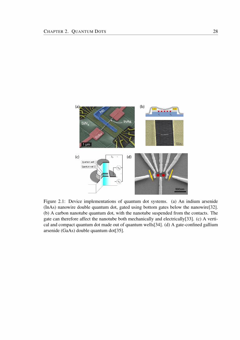
Figure 2.1: Device implementations of quantum dot systems. (a) An indium arsenide(InAs) nanowire double quantum dot, gated using bottom gates below the nanowire[32].(b) A carbon nanotube quantum dot, with the nanotube suspended from the contacts. Thegate can therefore affect the nanotube both mechanically and electrically[33]. (c) A verti-cal and compact quantum dot made out of quantum wells[34]. (d) A gate-confined galliumarsenide (GaAs) double quantum dot[35].
CHAPTER 2. QUANTUM DOTS 29
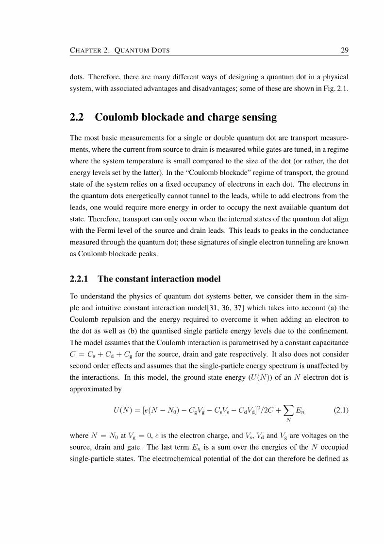
dots. Therefore, there are many different ways of designing a quantum dot in a physicalsystem, with associated advantages and disadvantages; some of these are shown in Fig. 2.1.
2.2 Coulomb blockade and charge sensing
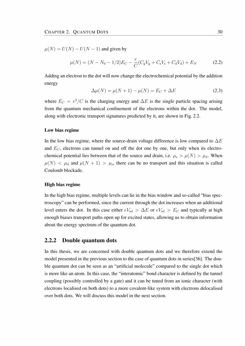
The most basic measurements for a single or double quantum dot are transport measure-ments, where the current from source to drain is measured while gates are tuned, in a regimewhere the system temperature is small compared to the size of the dot (or rather, the dotenergy levels set by the latter). In the “Coulomb blockade” regime of transport, the groundstate of the system relies on a fixed occupancy of electrons in each dot. The electrons inthe quantum dots energetically cannot tunnel to the leads, while to add electrons from theleads, one would require more energy in order to occupy the next available quantum dotstate. Therefore, transport can only occur when the internal states of the quantum dot alignwith the Fermi level of the source and drain leads. This leads to peaks in the conductancemeasured through the quantum dot; these signatures of single electron tunneling are knownas Coulomb blockade peaks.
2.2.1 The constant interaction model
To understand the physics of quantum dot systems better, we consider them in the sim-ple and intuitive constant interaction model[31, 36, 37] which takes into account (a) theCoulomb repulsion and the energy required to overcome it when adding an electron tothe dot as well as (b) the quantised single particle energy levels due to the confinement.The model assumes that the Coulomb interaction is parametrised by a constant capacitanceC = Cs + Cd + Cg for the source, drain and gate respectively. It also does not considersecond order effects and assumes that the single-particle energy spectrum is unaffected bythe interactions. In this model, the ground state energy (U(N)) of an N electron dot isapproximated by
U(N) = [e(N −N0)− CgVg − CsVs − CdVd]2/2C +∑N
En (2.1)
where N = N0 at Vg = 0, e is the electron charge, and Vs, Vd and Vg are voltages on thesource, drain and gate. The last term En is a sum over the energies of the N occupiedsingle-particle states. The electrochemical potential of the dot can therefore be defined as
CHAPTER 2. QUANTUM DOTS 30
µ(N) = U(N)− U(N − 1) and given by
µ(N) = (N −N0 − 1/2)EC −e
C(CgVg + CsVs + CdVd) + EN (2.2)
Adding an electron to the dot will now change the electrochemical potential by the additionenergy
∆µ(N) = µ(N + 1)− µ(N) = EC + ∆E (2.3)
where EC = e2/C is the charging energy and ∆E is the single particle spacing arisingfrom the quantum mechanical confinement of the electrons within the dot. The model,along with electronic transport signatures predicted by it, are shown in Fig. 2.2.
Low bias regime
In the low bias regime, where the source-drain voltage difference is low compared to ∆E
and EC , electrons can tunnel on and off the dot one by one, but only when its electro-chemical potential lies between that of the source and drain, i.e. µs > µ(N) > µd. Whenµ(N) < µd and µ(N + 1) > µs, there can be no transport and this situation is calledCoulomb blockade.
High bias regime
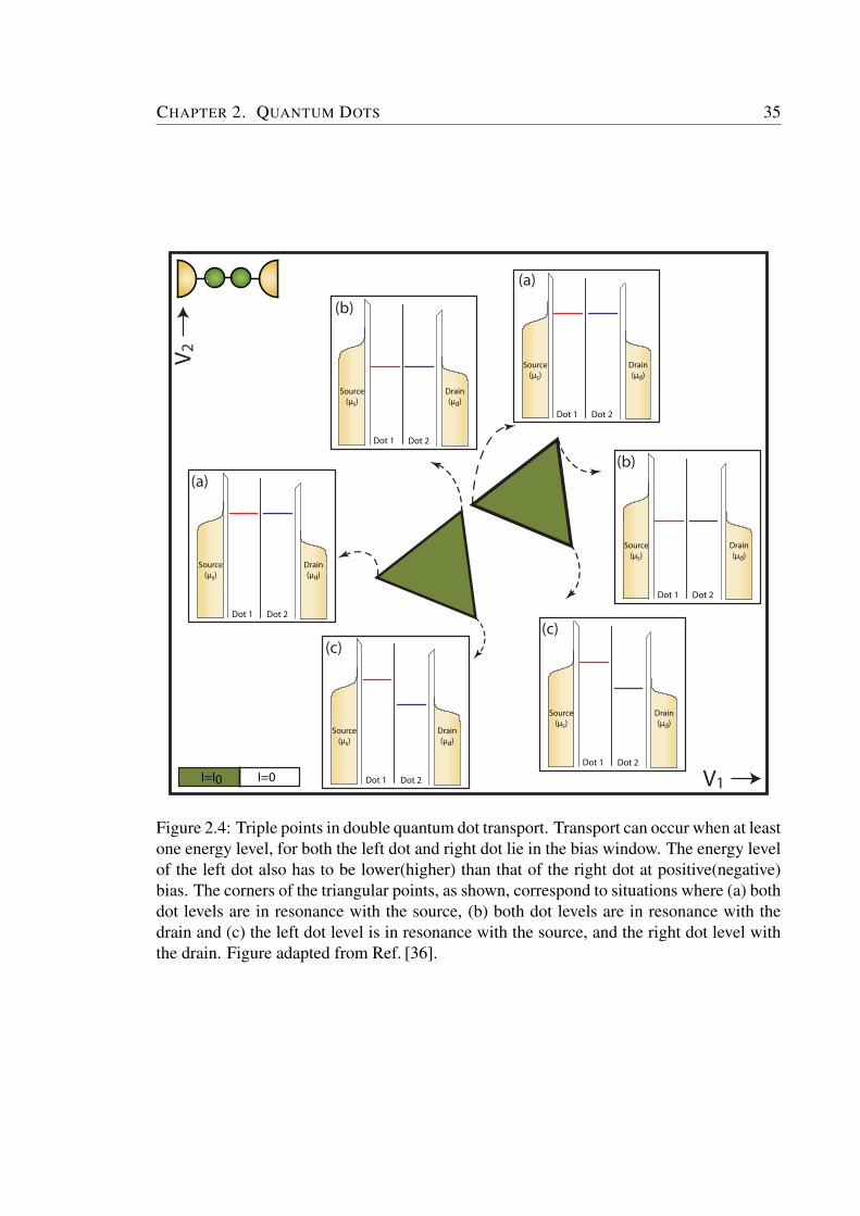
In the high bias regime, multiple levels can lie in the bias window and so-called “bias spec-troscopy” can be performed, since the current through the dot increases when an additionallevel enters the dot. In this case either eVsd > ∆E or eVsd > EC and typically at highenough biases transport paths open up for excited states, allowing us to obtain informationabout the energy spectrum of the quantum dot.
2.2.2 Double quantum dots
In this thesis, we are concerned with double quantum dots and we therefore extend themodel presented in the previous section to the case of quantum dots in series[36]. The dou-ble quantum dot can be seen as an “artificial molecule” compared to the single dot whichis more like an atom. In this case, the “interatomic” bond character is defined by the tunnelcoupling (possibly controlled by a gate) and it can be tuned from an ionic character (withelectrons localised on both dots) to a more covalent-like system with electrons delocalisedover both dots. We will discuss this model in the next section.
CHAPTER 2. QUANTUM DOTS 31
S
Rs
D
Vg
Cs RmCm
Rd
Cd
Cg
μ (N-1)
μs μd
μ (N)
μ (N+1)
μ (N-1)
μs μd
μ (N)
μ (N+1)
Vg
V sd I=0
Current
Source(μs)
Drain(μd)
μ (N)∆Vg
(a)
(b)
(c)
Vg (mV)
Gsd
(S)
Figure 2.2: Transport through a single quantum dot. (a) Circuit diagram showing resistiveand capacitive couplings to the source and drain, and the capacitive coupling to the gate. (b)The linear conductance with gate voltage shows Coulomb blockade, with current allowedto flow only when the dot level is aligned with the leads at zero bias. (c) At finite bias, thereis an expanded window of gate voltage where current may flow, causing diamond-shapedregions of blockade (shown on the right). At high enough applied bias, multiple chargestates may lie within the window and current can flow through multiple channels. Figuresadapted from [36] and transport simulated in Matlab.
CHAPTER 2. QUANTUM DOTS 32
In the constant interaction model applied to the double quantum dot, the system ofconductors can be expressed as matrices (instead of constant as before), where the chargesat each node are linear function of the potentials, Q = CV, where C is the capacitancematrix. Proceeding as in the previous section, but with the matrix method, we find for theelectrochemical potential of dot 1
µ(N1, N2) = (N1 − 1/2)EC1 +N2ECm −1
|e|(Cg1Vg1EC1 + Cg2Vg2ECm) (2.4)
EC1 is the change in the potential of dot 1 when (with gate voltage fixed), N1 is changedby 1, and is called the addition energy of dot 1, with EC2 the addition energy of dot 2. Themutual charging energy ECm gives the change in the energy of one dot when an electron isadded to the other. These energies are given by
EC1 =e2
C1
1
1− C2m
C1C2
EC2 =e2
C2
1
1− C2m
C1C2
ECm =e2
Cm
1
1− C1C2
C2m−1
(2.5)
In practice it is useful to define the reduced gate voltage ng = CgVg/ |e|, the polarizationcharge applied by the gate in electron units. If ng is some integer N , the dot obtains Nelectrons, while for a half-integer value of ng, electrons can move on and off the dot (thesingle-electron tunneling state). Coulomb blockade for a double quantum dot (when N isan integer) results in lines of stable charge configurations which change in shape dependingon the interdot tunnel coupling. Fig. 2.3 shows the shape of the transport configurationsagainst the individual dot gate voltages for the limiting cases of weak coupling (Cm = 0)and strong coupling (Cm/C1(2) → 1), as well as for the typical case where the coupling isintermediate. The charge stability diagram is then made up of hexagonal regions of fixedcharge, leading to the so-called honeycomb charge diagram. In this situation in the lowbias regime, transport through the double dot is permitted where the boundaries of threehexagonal regions meet, called “triple points”; this is where the potentials of the two dotsare aligned with the potentials of the leads. In the high bias regime the triple points nowbecome triangular regions, where two dot levels can lie in the bias window, as shown inFig. 2.4. Lastly, considering that the dot levels are quantised, for large voltages, ground
CHAPTER 2. QUANTUM DOTS 33
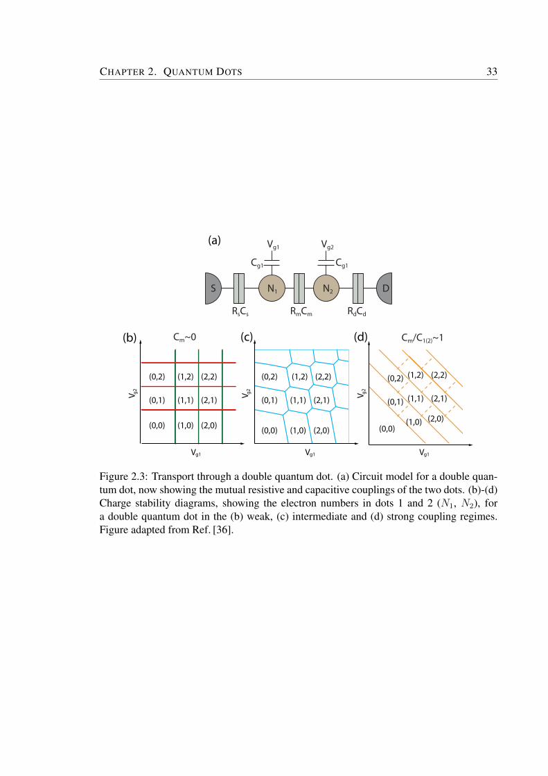
S N1
Cg1 Cg1
N2 D
Vg1 Vg2
RsCs RmCm RdCd
(0,0) (1,0) (2,0)
(2,1)(1,1)(0,1)
(0,2) (1,2) (2,2)
(0,0) (1,0) (2,0)
(2,1)(1,1)(0,1)
(0,2) (1,2) (2,2)
(0,0)(1,0) (2,0)
(2,1)(1,1)(0,1)
(0,2) (1,2) (2,2)
(b) (c) (d)
Vg1
V g2
V g2 V g2
Vg1 Vg1
(a)
Cm~0 Cm/C1(2)~1
Figure 2.3: Transport through a double quantum dot. (a) Circuit model for a double quan-tum dot, now showing the mutual resistive and capacitive couplings of the two dots. (b)-(d)Charge stability diagrams, showing the electron numbers in dots 1 and 2 (N1, N2), fora double quantum dot in the (b) weak, (c) intermediate and (d) strong coupling regimes.Figure adapted from Ref. [36].
CHAPTER 2. QUANTUM DOTS 34
states as well as excited states contribute to the transport. The successive alignment ofground and excited states contributes to resonances within the bias triangles. Transportmeasurements are useful for estimating charging energies, dot configurations and tunnelrates (the bending of the edges of the stability diagram with strong tunnel couplings, forexample, is useful for this). However, transport requires the exchange of dot electrons withleads, and therefore is inherently an invasive method. Qubit occupation can alternativelybe determined by the technique of charge sensing, where the capacitance or resistanceof a proximal charge sensor, sensitive to electrons tunnelling into and out of the dot ismonitored. Quantum point contact (QPCs), single electron transistors (SETs) as well asquantum dots are typically used for charge sensing. In addition, gate-based charge sensing,a method that has become popular over the last few years, can be used and is described inChapter 3.
We now discuss two kinds of two level systems or qubit candidates that are describedin this thesis and that can be realised using double quantum dot systems. The first kind isthe charge qubit.
2.3 Charge qubits
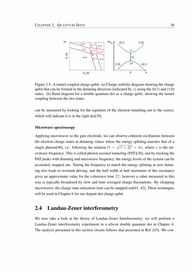
We have discussed how the ionic and covalent type states form in the weak and strong limitsof the tunnel coupling in a double quantum dot[38]. The one-electron charge states (0,1)and (1,0), i.e. whether the electron is on the right dot or the left, form the basis states |0〉and |1〉 of a charge qubit, shown in Fig. 2.5. We define the “detuning”, ε, as the gate voltageparameter which takes us across the (1,0) and (0,1) interdot charge transition (ICT) and setsthe energy splitting. Therefore we have the diagonal matrix element of the Hamiltonian,H = ε
2σz. The tunnel coupling (tc = ∆/2) gives the off-diagonal terms in the Hamiltonian,
leading to a full Hamiltonian of the form
Hi(t) = −∆
2σx −
ε
2σz (2.6)
and a splitting between the eigenenergies of Ω =√ε2 + ∆2 at the avoided crossing near
zero detuning.For charge qubits, by preparing a state with the electron in one dot (say, the left, at
ε0 < 0) followed by a pulse on the drain to zero detuning, one can make the system undergocoherent state mixing. When the device is switched back to ε0, the electron charge state
CHAPTER 2. QUANTUM DOTS 35
Dot 1
Source(μs)
Drain(μd)
Dot 2
Dot 1
Source(μs)
Drain(μd)
Dot 2
Dot 1
Source(μs)
Drain(μd)
Dot 2
Dot 1
Source(μs)
Drain(μd)
Dot 2
Dot 1
Source(μs)
Drain(μd)
Dot 2
Dot 1
Source(μs)
Drain(μd)
Dot 2
I=I0 I=0
(a)
(a)
(b)
(b)
(c)(c)
V1
V 2
Figure 2.4: Triple points in double quantum dot transport. Transport can occur when at leastone energy level, for both the left dot and right dot lie in the bias window. The energy levelof the left dot also has to be lower(higher) than that of the right dot at positive(negative)bias. The corners of the triangular points, as shown, correspond to situations where (a) bothdot levels are in resonance with the source, (b) both dot levels are in resonance with thedrain and (c) the left dot level is in resonance with the source, and the right dot level withthe drain. Figure adapted from Ref. [36].
CHAPTER 2. QUANTUM DOTS 36
V2 (V)
V 1(V
)
(1, 0)
(0, 1)
(1, 1)
(2, 0)
(0, 0)
(2, 1) (2, 2)
(1, 2)
(0, 2)
(a) (b) E
2tC
0 ε
|e›
|g›
ε
(1,0) (0,1)
(1,0)(0,1)
Figure 2.5: A tunnel coupled charge qubit. (a) Charge stability diagram showing the chargequbit that can be formed in the detuning direction (indicated by ε), using the (0,1) and (1,0)states. (b) Band diagram for a double quantum dot as a charge qubit, showing the tunnelcoupling between the two states.
can be measured by looking for the signature of the electron tunneling out to the source,which will indicate it is in the right dot[39].
Microwave spectroscopy
Applying microwaves to the gate electrode, we can observe coherent oscillations betweenthe electron charge states at detuning values where the energy splitting matches that of asingle photon[40], i.e. following the relation Ω =
√ε2 + ∆2 = hν, where ν is the mi-
crowave frequency. This is called photon assisted tunneling (PAT)[36], and by tracking thePAT peaks with detuning and microwave frequency, the energy levels of the system can beaccurately mapped out. Tuning the frequency to match the energy splitting at zero detun-ing also leads to resonant driving, and the half width at half maximum of this resonancegives an approximate value for the coherence time T ∗2 ; however a value measured in thisway is typically broadened by slow and time averaged charge fluctuations. By choppingmicrowaves, the charge state relaxation time can be mapped out[41, 42]. These techniqueswill be used in Chapter 6 for our dopant-dot charge qubit.
2.4 Landau-Zener interferometry
We now take a look at the theory of Landau-Zener Interferometry; we will perform aLandau-Zener interferometry experiment in a silicon double quantum dot in Chapter 4.The analysis presented in this section closely follows that presented in Ref. [43]. We con-
CHAPTER 2. QUANTUM DOTS 37
sider our charge qubit as a strongly and periodically driven two level system (TLS), withenergy bias or detuning ε(t) and tunnelling amplitude ∆, where the latter in our system isfixed. For such a TLS, the Hamiltonian in terms of the Pauli matrices σx,z can be written as
Hi(t) = −∆
2σx −
ε(t)
2σz (2.7)
We also assume periodic driving with amplitude A, angular frequency ω and offset ε0, suchthat
ε(t) = ε0 + A sinωt (2.8)
The instantaneous eigenvalues ofH(t) are
E±(t) = ±1
2Ω(t)
Ω(t) =√
∆2 + ε(t)2
(2.9)
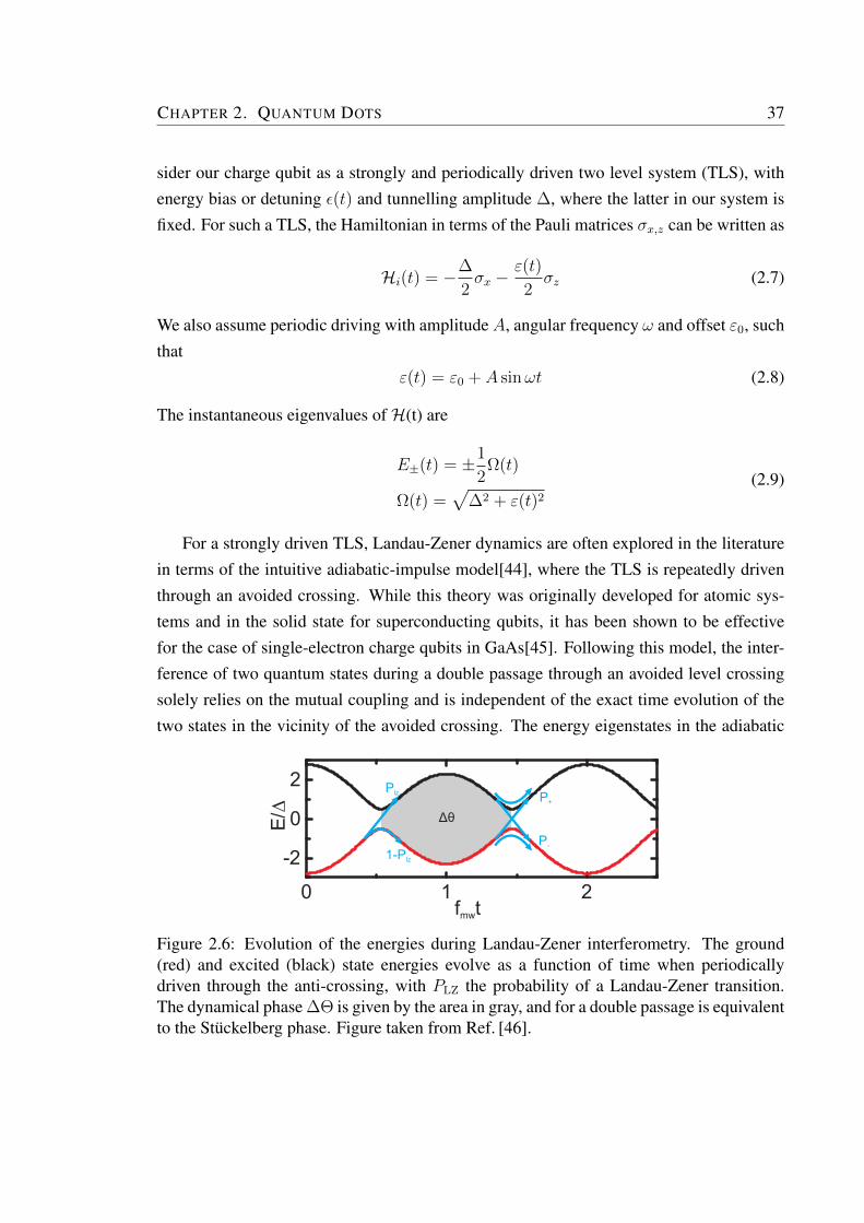
For a strongly driven TLS, Landau-Zener dynamics are often explored in the literaturein terms of the intuitive adiabatic-impulse model[44], where the TLS is repeatedly driventhrough an avoided crossing. While this theory was originally developed for atomic sys-tems and in the solid state for superconducting qubits, it has been shown to be effectivefor the case of single-electron charge qubits in GaAs[45]. Following this model, the inter-ference of two quantum states during a double passage through an avoided level crossingsolely relies on the mutual coupling and is independent of the exact time evolution of thetwo states in the vicinity of the avoided crossing. The energy eigenstates in the adiabatic
Plz
1-Plz
P+
P-
Δθ
ff tmw
Figure 2.6: Evolution of the energies during Landau-Zener interferometry. The ground(red) and excited (black) state energies evolve as a function of time when periodicallydriven through the anti-crossing, with PLZ the probability of a Landau-Zener transition.The dynamical phase ∆Θ is given by the area in gray, and for a double passage is equivalentto the Stuckelberg phase. Figure taken from Ref. [46].
CHAPTER 2. QUANTUM DOTS 38
basis change very fast around the avoided-crossing region, and remain more or less constantaway from the crossing; we therefore intuitively expect that the system evolves adiabati-cally away from the avoided crossing. However, the evolution becomes nonadiabatic nearthe anticrossing. Instead of making an arbitrary boundary between the nonadiabatic andadiabatic regimes, it is mathematically simpler to consider adiabatic evolution everywhereexcept at zero detuning, where a sudden mixing in the populations of the two energy levelsis modelled. This picture is called the adiabatic-impulse approximation, which emphasizesthe two-stage model and the instantaneous nature of the non-adiabatic transitions acrossthe avoided crossing.
Single Passage: The full derivation of the Landau-Zener probability is given inRef. [43], and we do not reproduce it here but discuss the results in different regimes. If weassume that the system initially occupies the lower energy level, the transition probabilityfrom the lower to the upper level during a single sweep across the avoided crossing canbe described within a quasiclassical approximation[47] (we will consider the effects ofdecoherence later), and the probability that the system ends up in the upper energy level isgiven by
P+ = PLZ = exp
[− π∆2
2ω√A2 − ε2
0
], (2.10)
where PLZ is the probability of a Landau-Zener transition. For small ∆ this implies thatthe probability rapidly changes along the lines |ε0| = A, and is constant in between. Theinclination of these lines can be compared with experiment for the calibration of microwaveamplitude. Defining the driving velocity v = ω
√A2 − ε2
0 leads us to see that as we vary vfrom 0 in the adiabatic limit to∞ in the sudden-change limit, the probability of the statetransitioning from the lower to upper level P+ goes from 0 to 1. As we will discuss next,this feature can be exploited by varying v such that the transition acts as a 50/50 beamsplitter for the electron wavefunction.
Double Passage and the Stuckelberg Phase: We now consider now the double-passage problem, where we traverse the avoided crossing region twice at the same speed (ordrive back and forth across the crossing), completing one full driving cycle of the periodicdrive. The probability of the system ending up in the upper basis can now be given by
P+ = 4PLZ(1− PLZ) sin2 ΦSt, (2.11)
CHAPTER 2. QUANTUM DOTS 39
which comes out to be
P+ ' 2π∆2
Aω
(1− ε2
0
A2
)−1/2
sin2 ΦSt, (2.12)
ΦSt = −ε0
ωarccos
ε0
A+A
ω
(1− ε2
0
A2
)1/2
− π
4. (2.13)
where ΦSt is the Stuckelberg phase[48, 49]. This situation is shown in Fig. 2.6. The prob-ability of the system being excited into the upper state after two consecutive passagesthrough the avoided crossing is therefore an oscillating function of this phase, the two com-ponents of which are acquired during the adiabatic evolution and non-adiabatic (impulse)transition. Without interference, the averaged probability is 〈P+〉 = 2PLZ(1− PLZ). How-ever, the quantum mechanical interference between the different LZ transitions means thatthe total excitation probability after both passages ranges from 0 for destructive interfer-ence to 〈P+〉 = 4PLZ(1− PLZ) for constructive interference, similar to the Mach-Zehnderinterferometer[50, 51].
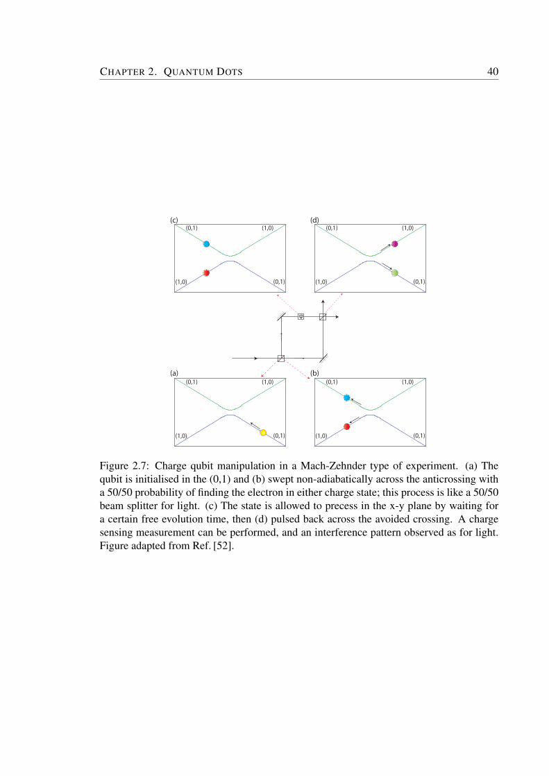
This kind of double-passage experiment presents a way to perform coherent chargestate manipulation. Fig. 2.7 shows the steps involved in such an experiment. Choosing aninitial state (0,1), the ground state at ε > 0, we adiabatically sweep across zero detuning.Now the ground state is (1,0). For a non-adiabatic sweep, the population mostly remainsin the initial state (1,0). The speed of the pulse across zero detuning can be set such thatthe resulting qubit state contains 50% of (1,0) and (0,1); this analogous to an optical 50/50beam splitter for light. This can be quantified by the Landau-Zener formula for singlepassage (Eq. 2.10).
After the beam-splitting pulse, the qubit can precess effectively in the x-y plane of theBloch sphere (with the Larmor frequency proportional to Ω until a refocusing pulse acrossthe anticrossing takes it back to the initial state (0,1)). The probability of finding the qubitin the initial state will now show a Mach-Zehnder type interference pattern with the qubitstates as the light paths, and coherent manipulation can be achieved by the tuning of pulselengths[51, 53].
Multiple Passage: The characteristic speckled LZS interference pattern is one thatarises from a multiple passage experiment, where the system is swept across the avoidedcrossing periodically. Some relevant timescales here for a visible interference pattern are(a) the time between subsequent tunneling events, which is of the order of half of thedriving period (T/2 = π/ω) and (b) the phase coherence of the system, for which we
CHAPTER 2. QUANTUM DOTS 40
(1,0)
φ
(1,0)(0,1)
(0,1) (1,0)
(1,0)(0,1)
(0,1)
(1,0)
(1,0)(0,1)
(0,1)(1,0)
(1,0)(0,1)
(0,1)
(a) (b)
(d)(c)
Figure 2.7: Charge qubit manipulation in a Mach-Zehnder type of experiment. (a) Thequbit is initialised in the (0,1) and (b) swept non-adiabatically across the anticrossing witha 50/50 probability of finding the electron in either charge state; this process is like a 50/50beam splitter for light. (c) The state is allowed to precess in the x-y plane by waiting fora certain free evolution time, then (d) pulsed back across the avoided crossing. A chargesensing measurement can be performed, and an interference pattern observed as for light.Figure adapted from Ref. [52].
CHAPTER 2. QUANTUM DOTS 41
consider the dephasing time T2. The characteristic Landau-Zener time (tLZ ∼ 2∆
∆2
4ω√A2−ε2 )
for the duration of a transition should therefore be tLZ < T/2 < T2, such that consecutiveLZ events cannot overlap, and that the phase coherence of the system is preserved.
The interference patterns observed can be vastly different depending on this character-istic Landau-Zener time; in the two opposite limits where the individual crossings are slow(such that they are almost adiabatic, and PLZ 1), or fast. In both cases, there is a res-onance condition which determines whether there will be an interference pattern betweenthe upper and lower states. In the LZS experiment explored in Chapter 4, we are in the fastpassage regime
∆2/Aω 1, (1− PLZ) 1 (2.14)
and therefore we concentrate on the description of this regime (the slow passage regime isdescribed further in Ref. [43]). The resonance condition here can be analytically calculated;it reduces to ε = kω for integer k. Changing the system parameters (ε0 or ω), we passthrough different k-photon resonances; this can give us a valuable energy scaling as well.Additionally, to calibrate the microwave power applied, one can use the separation betweenthe minima or maxima in the interference pattern (Fig. 2.8, described later, shows someLZS patterns).
In the analysis before, we have ignored decoherence (or rather, assumed T/2 T2).From the full calculations including the relaxation and dephasing times T1 and T2 (theseare performed in the rotating wave approximation using the Bloch equations for the re-duced density matrix, detailed in [43], Appendix B), the steady state solution for the time-averaged upper-level probability in the strong-driving regime is:
P+ =1
2
∑k
∆2k
∆2k + T2
T1(|ε0| − k~ω)2 + ~2
T1T2
, (2.15)
where ∆k = ∆Jk(A/~ω), and Jk is the k-th order Bessel function. This formula is a goodapproximation everywhere except for the vicinity of ε0 = 0 (however it is still qualitativelyilluminative in this region, as we will see in our simulations in Chapter 4). It is worth notingthat this formula additionally describes the single and double passage cases, with the effectof decoherence included.
CHAPTER 2. QUANTUM DOTS 42
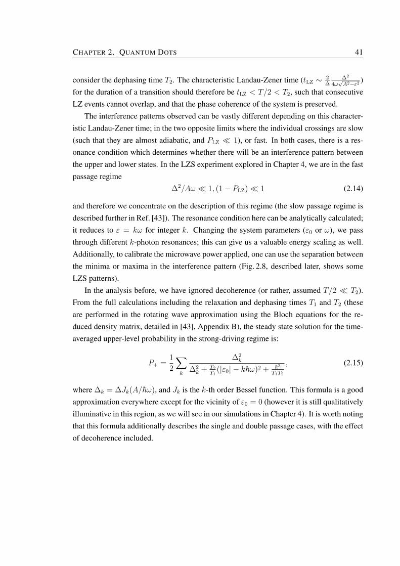
Decoherence and the Landau-Zener problem
For LZS interferometry, it is useful to consider a fast-driven TLS where we start with in-coherent driving (slow compared to T2) and gradually increase the coherence time of thesystem[43]. We look at the effect of coherence on the steady-state populations of the twolevels. With strong decoherence, no interference occurs between the different Landau-Zener transitions. In this case, going back and forth through the avoided crossing, we givea small impulse (uncorrelated to impulses from all the other sweeps) to the state popula-tions, which adds up to a steady state where the two states have equal populations of thetwo energy levels (the exact ratio depends on thermal excitation and relaxation rates). Thisis shown in Fig. 2.8(a). We now increase the coherence time to a point where the two transi-tions in a single driving period (i.e. driving back and forth) are separated by a time smallerthan T2. However, the transitions induced by two different driving cycles are separated bymore than T2, and these are then independent impulses. There are therefore two interferingtransitions per cycle, and if the phase accumulated between these corresponds to destruc-tive interference, at the end of a full driving period there will be no mixing. There will nowbe lines in the previously incoherent map, as shown in Fig. 2.8(b). We can now increaseT2 even more, such that we can interfere between transitions from a few successive driv-ing cycles. The resonance lines now start forming; indicating that the mixing between thetwo states is suppressed whenever the resonance condition presented in Section 2.4 is notsatisfied (Fig. 2.8(c)).
Figure 2.8: Effect of decoherence on the Landau-Zener interferometry pattern. LZS in-terferometry with high-frequency driving is shown, including the effects of decoherence,by numerically solving Eq. 2.15, with the upper level steady state probability plotted. Thedephasing time T2 is given by ωT2/(2π) = 0.1 in (a), 0.5 in (b) and 1 in (c), while therelaxation time is given by ωT1/(2π) = 103 for all plots. Figure adapted from Ref. [43].
In Chapter 4 we will revisit the LZS formulas, with some modifications due to thetechnique of gate-based reflectometry and the measurement via the quantum capacitance.
CHAPTER 2. QUANTUM DOTS 43
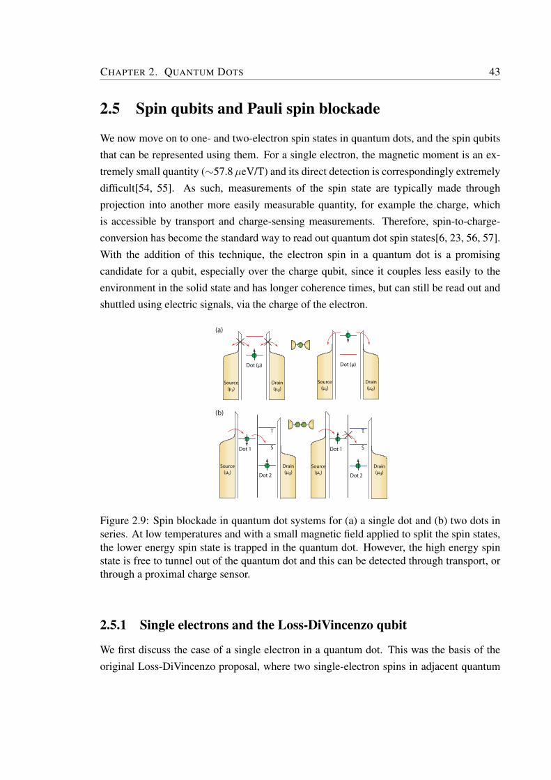
2.5 Spin qubits and Pauli spin blockade
We now move on to one- and two-electron spin states in quantum dots, and the spin qubitsthat can be represented using them. For a single electron, the magnetic moment is an ex-tremely small quantity (∼57.8µeV/T) and its direct detection is correspondingly extremelydifficult[54, 55]. As such, measurements of the spin state are typically made throughprojection into another more easily measurable quantity, for example the charge, whichis accessible by transport and charge-sensing measurements. Therefore, spin-to-charge-conversion has become the standard way to read out quantum dot spin states[6, 23, 56, 57].With the addition of this technique, the electron spin in a quantum dot is a promisingcandidate for a qubit, especially over the charge qubit, since it couples less easily to theenvironment in the solid state and has longer coherence times, but can still be read out andshuttled using electric signals, via the charge of the electron.
Dot (μ)
Source(μs)
Drain(μd)
Dot (μ)
Source(μs)
Drain(μd)
Dot 1
Source(μs)
Drain(μd)Dot 2
S
T
Dot 1
Source(μs)
Drain(μd)Dot 2
S
T
(a)
(b)
Figure 2.9: Spin blockade in quantum dot systems for (a) a single dot and (b) two dots inseries. At low temperatures and with a small magnetic field applied to split the spin states,the lower energy spin state is trapped in the quantum dot. However, the high energy spinstate is free to tunnel out of the quantum dot and this can be detected through transport, orthrough a proximal charge sensor.
2.5.1 Single electrons and the Loss-DiVincenzo qubit
We first discuss the case of a single electron in a quantum dot. This was the basis of theoriginal Loss-DiVincenzo proposal, where two single-electron spins in adjacent quantum
CHAPTER 2. QUANTUM DOTS 44
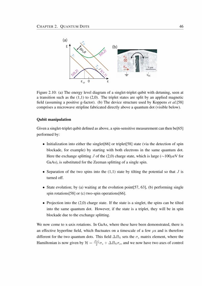
dots formed two qubits, with each two level system formed of the |↑〉 and |↓〉 spin statessplit by the Zeeman energy (EZ) in a large external magnetic field B0 (∼1 T). This kind ofqubit relies on a kind of spin blockade; when the quantum dot is tuned correctly, the energydifference between the two spin states under B0 means that tunneling is allowed for oneorientation of the spin, and blocked for the other (Fig. 2.9). Manipulation of the spin canbe accomplished using Electron Spin Resonance, or ESR. For example, microwave pulsesat resonance (hν = EZ) can be applied to an on-chip transmission line to create an ACmagnetic field B1, driving rotations between |↑〉 and |↓〉. In 2006, this technique was firstdemonstrated by Koppens et al.[58] in a GaAs quantum dot that had a microwave striplinefabricated on top, shown in Fig. 2.10(b).
For double quantum dots, a two qubit logic gate has been performed in silicon[18],using a similar technique. A microwave stripline addresses two adjacent spins in a doublequantum dot, with a small frequency difference of 40 MHz that is electrically tuned via theStark shift. In this case, the readout is hysteretic; tunneling of dot 1 to the reservoir is viadot 2, leading to hysteresis as a function of the sweeping direction since there is a finitemutual charging energy. Dot 1 can only tunnel to dot 2 and then to the reservoir when thedot levels are aligned, leading to a charge-sensing signal that is maximised in this situation.
ESR has also been demonstrated using an oscillating electric field applied to a gateelectrode[59]. This method is preferable since it avoids the fabrication of a separatestripline, which is typically large compared to the quantum dot dimensions and thereforeaffects scalability. However, this method generates the effective AC B1 field by moving theelectron wavefunction using the AC-electric field in an external magnetic field gradient.Such a gradient can be generated using a micromagnet[60, 61] or by random variations inthe nuclear magnetic field[62], or alternatively by spin orbit coupling[59] (giving rise toElectron Dipole Spin Resonance or EDSR). In our experiments in Chapter 6, we show thatanother method of generating a gradient could be built into our hybrid dopant-dot system,since an electron localised on the dopant feels the contact hyperfine interaction from thenuclear spin, which it does not while localised on the dot. Measurements hinting at thisprocess, with rotations driven using the natural field gradient due to a phosphorus atomhave recently been reported[30].
In single-spin quantum dots, the DiVincenzo[20] criteria have largely been met, in sil-icon as well as in other materials. However, the schemes above have the disadvantage thatthey require high magnetic fields to provide high Zeeman splittings, which can affect co-herence in certain systems[63] which operate better at low magnetic fields. In addition,
CHAPTER 2. QUANTUM DOTS 45
micromagnets and coplanar striplines are difficult to scale up, and silicon has a very weakspin-orbit coupling as well as a lack of a strong fluctuating nuclear magnetic field. Analternative method therefore focuses on two-electron spin states, and is outlined below.
2.5.2 Two electrons and the singlet-triplet qubit
For two electrons, we have the following four two-spin states, the antisymmetric singlet
|S〉 = (|↑↓〉 − |↓↑〉)/√
2 (2.16)
with S = 0 and the symmetric triplets
|T+〉 = |↑↑〉
|T0〉 = (|↑↓〉+ |↓↑〉)/√
2
|T−〉 = |↓↓〉
(2.17)
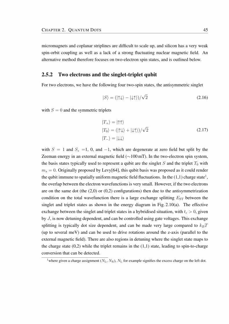
with S = 1 and Sz =1, 0, and −1, which are degenerate at zero field but split by theZeeman energy in an external magnetic field (∼100 mT). In the two-electron spin system,the basis states typically used to represent a qubit are the singlet S and the triplet T0 withms = 0. Originally proposed by Levy[64], this qubit basis was proposed as it could renderthe qubit immune to spatially uniform magnetic field fluctuations. In the (1,1) charge state1,the overlap between the electron wavefunctions is very small. However, if the two electronsare on the same dot (the (2,0) or (0,2) configurations) then due to the antisymmetrizationcondition on the total wavefunction there is a large exchange splitting EST between thesinglet and triplet states as shown in the energy diagram in Fig. 2.10(a). The effectiveexchange between the singlet and triplet states in a hybridised situation, with tc > 0, givenby J , is now detuning dependent, and can be controlled using gate voltages. This exchangesplitting is typically dot size dependent, and can be made very large compared to kBT
(up to several meV) and can be used to drive rotations around the z-axis (parallel to theexternal magnetic field). There are also regions in detuning where the singlet state maps tothe charge state (0,2) while the triplet remains in the (1,1) state, leading to spin-to-chargeconversion that can be detected.
1where given a charge assignment (NL, NR), NL for example signifies the excess charge on the left dot.
CHAPTER 2. QUANTUM DOTS 46
T+
S(0,2)
E
0 ε
T0 / S(1,1)
T -
S(0,2)
ε ST
gμB B
(a)(b)
Figure 2.10: (a) The energy level diagram of a singlet-triplet qubit with detuning, seen ata transition such as the (1,1) to (2,0). The triplet states are split by an applied magneticfield (assuming a positive g-factor). (b) The device structure used by Koppens et al.[58]comprises a microwave stripline fabricated directly above a quantum dot (visible below).
Qubit manipulation
Given a singlet-triplet qubit defined as above, a spin-sensitive measurement can then be[65]performed by:
• Initialization into either the singlet[66] or triplet[58] state (via the detection of spinblockade, for example) by starting with both electrons in the same quantum dot.Here the exchange splitting J of the (2,0) charge state, which is large (∼100µeV forGaAs), is substituted for the Zeeman splitting of a single spin.
• Separation of the two spins into the (1,1) state by tilting the potential so that J isturned off.
• State evolution; by (a) waiting at the evolution point[57, 63], (b) performing singlespin rotations[58] or (c) two-spin operations[66].
• Projection into the (2,0) charge state. If the state is a singlet, the spins can be tiltedinto the same quantum dot. However, if the state is a triplet, they will be in spinblockade due to the exchange splitting.
We now come to x-axis rotations. In GaAs, where these have been demonstrated, there isan effective hyperfine field, which fluctuates on a timescale of a few µs and is thereforedifferent for the two quantum dots. This field ∆BN sets the σz matrix element, where theHamiltonian is now given by H = J(ε)
2σz + ∆BNσx, and we now have two axes of control
CHAPTER 2. QUANTUM DOTS 47
for our qubit[66]. In other systems such as silicon, where there is a much smaller hyperfinefield arising from the 29Si isotope (and no hyperfine field for isotopically purified 28Si)methods such as a coplanar stripline need to be used for this purpose[18].
Nuclear spin polarization
The last topic we touch upon for singlet-triplet qubits is the technique of nuclear spinpolarization. At the S − T− crossing shown in Fig. 2.10(a) (S − T+ for GaAs due to itsnegative g-factor), the effective exchange matches the Zeeman energy and any nuclear spingradient mixes the two states. This kind of transition is important for our proposed hybriddopant-dot spin qubit, as explored in Chapter 6. At such a mixed crossing, an S − T−
transition results in an electron spin flip; angular momentum conservation now requires asimultaneous spin ‘flop’, coming from a neighbouring nuclear spin in GaAs or in naturalSi, while for a dopant-dot hybrid qubit in 28Si, the dopant nuclear spin flip can be inducedin this way. Repeated transitions followed by exchange of electrons with the leads can thenbuild up a nuclear spin polarization[67]. Such polarization techniques have been shownto strongly increase the inhomogeneous coherence time T ∗2 [68] and in our system can beexplored as a way to access the dopant nuclear spin.
Lastly, we mention the exchange-only qubit[69, 70], which has been proposed for threespins in a triple quantum dot architecture. Rotations in such a qubit are mediated in bothx- and z-directions by the exchange interaction and this eliminates the need for direct orindirect magnetic control via micromagnets, striplines, or spin-orbit coupling and EDSR.While this system has been explored in GaAs quantum dots, it is yet to be implemented insilicon.
2.5.3 The silicon material system
In this section, we briefly describe the silicon semiconductor as host for quantum dot qubitsas described above, as compared with other systems such as GaAs heterostructures andInAs nanowires. In Chapter 1 we have presented silicon as an attractive host for a qubit ar-chitecture due to the presence of a multi-billion dollar semiconductor industry that is ableto make small scale silicon devices, complete with control electronics, with repeatabilityand ease. However, apart from these scalability considerations, silicon as a semiconduc-tor host for quantum dots has some specific advantages in terms of qubit relaxation andcoherence, which we now discuss.
CHAPTER 2. QUANTUM DOTS 48
Spin-orbit interaction
The decay of coherent Rabi oscillations, a measure of information loss, can be attributedto processes categorised as relaxation and decoherence. The relaxation timescale T1 isstrongly correlated with the spin-orbit coupling in the host material.
For a charge qubit, relaxation to the ground state is often mediated by phonons[31].However, for pure spin states, a spin-flip process is required, which phonons cannot causesince they carry no angular momentum. However in practice, the pure spin states we useto describe spin qubits are not totally ‘pure’ due to the presence of spin-orbit coupling,which couples the spin degree of freedom to the orbital levels[71]. The spin orbit couplingarises from the stretched lattice Coulomb potential (and consequently an effective magneticfield) seen by the relativistically moving conduction band electrons[72, 73]. This can bedecomposed into Dresselhaus[74] and Rashba[75] processes. The former, also called bulkinversion asymmetry, comes from the atomic cores of the host lattice, while the latter, alsocalled structure inversion asymmetry, consists of the macroscopic electric field into whichgate potentials also contribute. The spin-orbit interaction couples the pure spin states to theorbital levels, so that the spin and orbital quantum numbers are not good anymore. Phononscan now therefore participate in the relaxation process without the selection rules imposedearlier. Silicon has a weak spin-orbit coupling[76], due to its low atomic number and itsmonoatomic lattice, and this results in spin-orbit induced relaxation rates that are predictedto be at least two orders of magnitude smaller than for GaAs[77].
Hyperfine interaction
Decoherence of the spin qubit is described by T2, the time taken to lose coherent phaseinformation. Hyperfine-induced decoherence is a major contributor to the lower coherencetimes of GaAs spin qubits (where Rabi oscillations quickly decay on a scale of tens to hun-dreds of nanoseconds) as compared to silicon[62, 66]. The Zeeman splitting of a nuclearspin is typically much lower than realistic values of kBT , since the g-factor has a valuethat is 103 times lower. The direction of the nuclear spin is constantly fluctuating, leadingto a total hyperfine field that is a Gaussian distribution. Due to this fluctuating nature, theLarmor frequency also fluctuates, leading to decay of the Rabi oscillations that decay ase−t
2/T 22 where T2 ∝ ∆BN. To improve T2, apart from refocusing pulse sequences such
as CPMG[66], one can move to a host material with fewer nuclear spins. Silicon has alow concentration of nuclear spins arising from the low-abundance 29Si isotope (only 5%),
CHAPTER 2. QUANTUM DOTS 49
and it can be further isotopically purified to the 28Si isotope, which results in a kind of“semiconductor vacuum” for spin.
One disadvantage, however, which should be mentioned at this point is that the ∼3times larger effective mass of silicon as compared to GaAs leads to a need for scaling downalready small gate configurations in order to form quantum dots with adequate orbital levelspacings (by a factor of about ∼2.5 for a typical depletion-gate geometry as shown inFig. 2.1(d)). We discuss this fabrication challenge, and a potential solution to it, in moredetail in the following chapter.
Lastly, we discuss a final obstacle for silicon, its six-fold degenerate valleys. These aresix equivalent conduction-band minima located on the ∆ lines, at k ≈ 0.84k0 toward the sixX-points of the Brillouin zone[78]. Due to confinement in the z-direction and/or uniaxialtensile strain at the interface, the valleys perpendicular to the interface have a much smallerenergy than those in the plane of the interface. The two z-valleys can be further coupled bya sharp interface, with a valley-orbit coupling ∆ which is sample and interface dependent(for example for Si/SiGe and Si/SiO2)[77]. A large valley splitting is desired since thedegenerate system then reduces to a single-valley qubit, a nuclear-spin free version of thevery successful GaAs system. On the other hand, for smaller valley splittings, the energyscale is no longer set by the confinement but by the valley splitting and it can becomedifficult to observe spin blockade since it can be lifted by the valley degree of freedom.
In the next section, we discuss the other component of our hybrid qubit, the dopant spinin silicon.
2.6 Dopant spins in silicon
Up to now we have discussed quantum dots in the solid state. In this section, we presenta few aspects of the physics of dopant atoms, and especially their spins, in silicon. Inparticular, electron spin resonance has been used for decades to measure and manipulatedopant spins in silicon, and is a technique we will apply in the measurements presented inthe later chapters of this thesis.
For the sake of simplicity, we consider the 31P donor in silicon, which can be conceptu-alised as a hydrogen atom in a solid state matrix. It has the excess charge of the phosphorusnucleus as compared to the silicon nuclei, creating a Coulomb potential that can bind anextra electron in the neutral donor (D0) charge state. The nucleus has a spin I = 1/2 (this
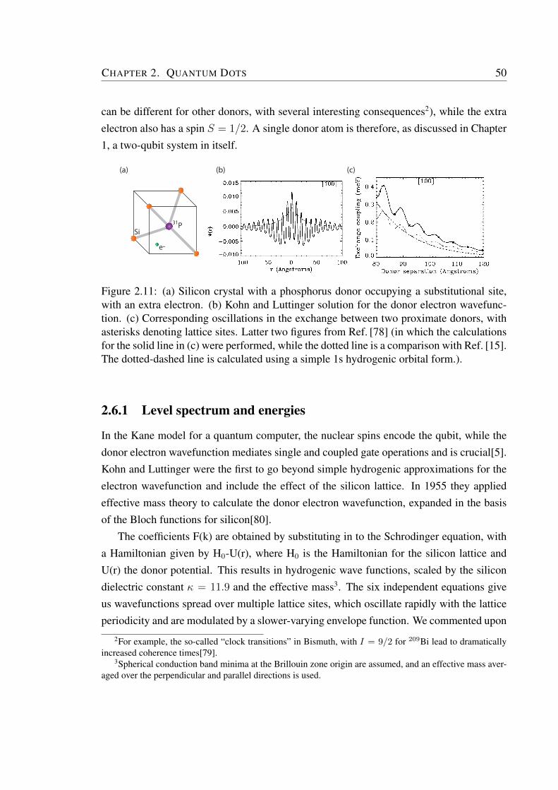
CHAPTER 2. QUANTUM DOTS 50
can be different for other donors, with several interesting consequences2), while the extraelectron also has a spin S = 1/2. A single donor atom is therefore, as discussed in Chapter1, a two-qubit system in itself.
e-
31PSi
(a) (b) (c)
Figure 2.11: (a) Silicon crystal with a phosphorus donor occupying a substitutional site,with an extra electron. (b) Kohn and Luttinger solution for the donor electron wavefunc-tion. (c) Corresponding oscillations in the exchange between two proximate donors, withasterisks denoting lattice sites. Latter two figures from Ref. [78] (in which the calculationsfor the solid line in (c) were performed, while the dotted line is a comparison with Ref. [15].The dotted-dashed line is calculated using a simple 1s hydrogenic orbital form.).
2.6.1 Level spectrum and energies
In the Kane model for a quantum computer, the nuclear spins encode the qubit, while thedonor electron wavefunction mediates single and coupled gate operations and is crucial[5].Kohn and Luttinger were the first to go beyond simple hydrogenic approximations for theelectron wavefunction and include the effect of the silicon lattice. In 1955 they appliedeffective mass theory to calculate the donor electron wavefunction, expanded in the basisof the Bloch functions for silicon[80].
The coefficients F(k) are obtained by substituting in to the Schrodinger equation, witha Hamiltonian given by H0-U(r), where H0 is the Hamiltonian for the silicon lattice andU(r) the donor potential. This results in hydrogenic wave functions, scaled by the silicondielectric constant κ = 11.9 and the effective mass3. The six independent equations giveus wavefunctions spread over multiple lattice sites, which oscillate rapidly with the latticeperiodicity and are modulated by a slower-varying envelope function. We commented upon
2For example, the so-called “clock transitions” in Bismuth, with I = 9/2 for 209Bi lead to dramaticallyincreased coherence times[79].
3Spherical conduction band minima at the Brillouin zone origin are assumed, and an effective mass aver-aged over the perpendicular and parallel directions is used.
CHAPTER 2. QUANTUM DOTS 51
the sixfold-degenerate valleys in the bandstructure of silicon in the previous section; thesehave consequences for the energy spectrum of the donors in silicon, and taking valley-orbit coupling into account accounts for much of the discrepancy observed between theKohn-Luttinger energy levels (28.95 meV) and the experimental values (45.5 meV). Furtherrefinements, bringing the energy levels into agreement with the experimental values, weremade using local empirical pseudopotential methods[15].
However, for the purposes of the Kane model of quantum computer, we are interestedin the donor wavefunction. Fig. 2.11 shows the wavefunction calculated in Refs. [15, 78]and the consequent calculated exchange energies versus donor separations. We can makethe observation that the exchange coupling is extremely sensitive to the relative orientationof the two phosphorus donors and oscillates rapidly with distance. This sets stringent re-quirements on the placement of donors for quantum computation architectures reliant onthe exchange interaction between two such atoms. As such, interfacing with other sys-tems to mediate interactions between dopants, instead of relying on interdonor exchangecouplings, is an attractive option.
Interface effects and the D− state
Two electron states for shallow donors have very small binding energies in bulk silicon,of the order of a few meV[81]. However, the binding energy of the donor is very muchaffected by the interface, and quantum confinement strongly increases the binding energy,for example in the case of the silicon nanowires studied in this thesis. For an As donor instrong electric field applied in a silicon transistor, not only was the D− shifted into a morebound configuration, a D− excited state, thought not to exist for donors in bulk silicon, wasobserved[82].
A second interesting consideration is that of effects seen when a donor is close to aninterface. While at low fields the electron is confined by the donor’s Coulombic potential,at higher fields (but before ionization) there is a potential well at the interface pulling thedonor electron up and away from the donor. However, even in this regime the electron isconfined laterally by the donor potential. Proposals have been made to exploit this effectfor quantum computation.
CHAPTER 2. QUANTUM DOTS 52
2.6.2 The donor spin system
We now discuss the spin system of the donor using a spin Hamiltonian approach. This iscrucial for understanding the excitation spectra in ESR experiments.
Using S and I as the donor electron and nuclear spin respectively, we can write downthe spin Hamiltonian as follows[83]
H = HZ +HH +HSS +HSO (2.18)
where the terms going into the Hamiltonian are the Zeeman, hyperfine, spin-spin interac-tion, and spin-orbit interaction energies.
The Zeeman term can be written (in frequency units) as follows:
HZ = γeB0 · S− γnB0 · I (2.19)
where γe = geµB/h is the electron gyromagnetic ratio, defined as positive, with ge is theelectron g-factor and B0 the static magnetic field. Similarly, γn = gnµn/h is the nucleargyromagnetic ratio, with gn the nuclear g-factor and µn the nuclear magneton, three ordersof magnitude smaller than that of the electron. The Lande g-tensor g entering into Eq. 2.19is generally anisotropic in crystals and is a consequence of spin-orbit coupling; since siliconhas very weak spin-orbit coupling, we can take g ≈ 2 for electrons in silicon. Silicon alsohas a sixfold degenerate valley structure, and the difference in effective mass results indifferent values of g within a valley. However, the valleys are equally populated in theground state and the electron sees an average of the g-factors, so that no anisotropy isexpected. However, this is important for silicon heterostructures (SiGe) and possibly forconfined nanostuctures.
The second term is the Hyperfine term, or the Fermi contact hyperfine interaction, aris-ing from the overlap of the electron wavefunction with the donor nucleus. This term isgiven by
HH = S ·A · I (2.20)
where A is the hyperfine tensor, which is mostly isotropic for the 1s state, and is propor-tional to the electron wavefunction at the nuclear site. This wavefunction can be tunedelectrically and can in turn tune the hyperfine interaction, forming the basis of the A-gatein the Kane architecture[5]. We discuss the different donor hyperfine splittings and theirconsequences in later chapters.
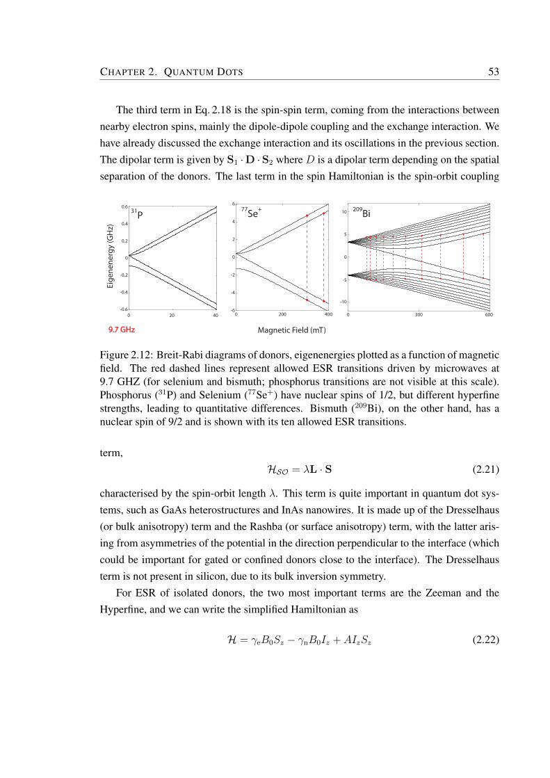
CHAPTER 2. QUANTUM DOTS 53
The third term in Eq. 2.18 is the spin-spin term, coming from the interactions betweennearby electron spins, mainly the dipole-dipole coupling and the exchange interaction. Wehave already discussed the exchange interaction and its oscillations in the previous section.The dipolar term is given by S1 ·D ·S2 where D is a dipolar term depending on the spatialseparation of the donors. The last term in the spin Hamiltonian is the spin-orbit coupling
0 20 40-0.6
-0.4
-0.2
0
0.2
0.4
0.6
0 300 600
-10
-5
0
5
10
0 200 400-6
-4
-2
0
2
4
6
Magnetic Field (mT)
Eige
nene
rgy
(GH
z)
31P77Se+ 209Bi
9.7 GHz
Figure 2.12: Breit-Rabi diagrams of donors, eigenenergies plotted as a function of magneticfield. The red dashed lines represent allowed ESR transitions driven by microwaves at9.7 GHZ (for selenium and bismuth; phosphorus transitions are not visible at this scale).Phosphorus (31P) and Selenium (77Se+) have nuclear spins of 1/2, but different hyperfinestrengths, leading to quantitative differences. Bismuth (209Bi), on the other hand, has anuclear spin of 9/2 and is shown with its ten allowed ESR transitions.
term,HSO = λL · S (2.21)
characterised by the spin-orbit length λ. This term is quite important in quantum dot sys-tems, such as GaAs heterostructures and InAs nanowires. It is made up of the Dresselhaus(or bulk anisotropy) term and the Rashba (or surface anisotropy) term, with the latter aris-ing from asymmetries of the potential in the direction perpendicular to the interface (whichcould be important for gated or confined donors close to the interface). The Dresselhausterm is not present in silicon, due to its bulk inversion symmetry.
For ESR of isolated donors, the two most important terms are the Zeeman and theHyperfine, and we can write the simplified Hamiltonian as
H = γeB0Sz − γnB0Iz + AIzSz (2.22)
CHAPTER 2. QUANTUM DOTS 54
where A is assumed to be isotropic. This Hamiltonian is isotropic and can be exactly solvedfor the eigenstates, the eigenenergies for which come out to be:
E↓⇑ =−√
(γ+B0)2 + A2 − A/22
E↓⇓ =−γ−B0 + A/2
2
E↑⇓ =
√(γ+B0)2 + A2 − A/2
2
E↑⇑ =γ−B0 + A/2
2
(2.23)
where γ± = γe ± γn and where the arrows indicate the orientation of the electron ↑) andnuclear (⇑) spin, and the energies are in frequency units. Fig. 2.12 shows the above eigenen-ergies versus magnetic field, plotted for the donors relevant to the experiments presented inthis thesis, 31P and 77Se (both with nuclear spin 1/2), as well as the allowed ESR transitionswhen applied microwaves of 9.7 GHz (X-band ESR) are used to generate the oscillatingAC magnetic field B1. We also include the energy spectrum of 209Bi, which has a nuclearspin of 9/2, to illustrate its rich Hilbert space which is relevant for the experiments exploredin Chapter 6.
In the remainder of this thesis, we present our experimental setup, as well as our effortstowards choosing a quantum dot architecture, selecting suitable donors, and finally, forminga dopant-dot hybrid qubit.
Chapter 3
Experimental Techniques
In this Chapter, we introduce the main experimental techniques used to perform the mea-surements in this thesis. First, we discuss the measurement of dopant spins via spin-to-charge conversion using the technique of electrically detected magnetic resonance, whichwe carry out in a cryostat that goes down to 4 Kelvin. Quantum dots and dopant spinscoupled to them typically require temperatures in the millikelvin range for their measure-ment, so that the relevant energy scales (such as the dot charging energies) are greater thankBT . For these transport and charge sensing measurements, millikelvin temperatures areachieved in a dilution fridge. We introduce the cryogenic setup, and the techniques of DCtransport as well as fast, sensitive gate-based RF-reflectometry. We also briefly present thefabrication of silicon quantum dot and dopant devices as well as the development of a flex-ible fabrication platform for making silicon devices with a high-quality interface. Lastly,we present one of the cornerstones of the results presented in this thesis, CMOS-silicon de-vices fabricated in an industry compatible foundry, and discuss their design, the mechanicsof quantum dot formation, and some aspects of performing measurements upon them.
3.1 Electrically Detected Magnetic Resonance
Electrically Detected Magnetic Resonance (EDMR) is a technique used to detect spin-dependent transport in the solid-state that can be orders of magnitude more sensitive thanESR, and is capable of detecting ensembles of fewer than 100 donors[84][85]. It has beena forerunner in the study of spin-to-charge conversion mechanisms such as spin-dependenttunneling which have been instrumental in the integration of dopants into devices. We nowdiscuss the measurement setup of EDMR used in the measurements shown in Chapter 5.
55
CHAPTER 3. EXPERIMENTAL TECHNIQUES 56
3.1.1 Electron Spin Resonance
ESR is a technique that can probe the spin degree of freedom for donors in silicon. The spinHamiltonian of a donor electron in a silicon crystal was presented in Chapter 2. Given astatic magnetic field B0, and ignoring the hyperfine coupling and other higher order terms,we find the resonance condition hν = gµBB0[83]. For the donors in silicon, which haveLande g-factors close to 2, microwave photons can drive spin resonance for Zeeman fieldsof a few Tesla. The magnetic field component of this oscillatory microwave field is perpen-dicular to B0 and is conventionally called B1.
In a typical ESR setup like the one shown in Fig. 3.1, a single-mode resonant microwavecavity (a cylindrical TE011 in our case) is inserted between the Helmholtz coils of an elec-tromagnet, and typically also immersed in a helium flow cryostat for cooling down to 4.2 K.Microwaves are generated by the microwave bridge, and the signal is split into two com-ponents. One is sent in to the sample and out through a circulator to be detected via aSchottky diode, while the second component is used as a reference for the demodulation.When the resonance condition given in the previous paragraph is satisfied, the sample ab-sorbs microwaves and this translates to a signal on the spectrometer. A field modulationtechnique is used to improve the signal-to-noise ratio. The magnetic field in a typical ESR(and EDMR) measurement is superimposed with an ac magnetic field Bmod, with a modu-lation frequency fmod typically 10–100 kHz, and the signal channel detects signals at thisac frequency only, via a lock-in technique. Our measurements are carried out in a BrukerElexsys E680 spectrometer with an X-band resonator (X-band measurements are carriedout at microwave frequencies of 9–10 GHz and fields of ∼0.35 T), shown in Fig. 3.1(a).
One limitation of the EPR technique is the requirement for a large ensemble of spins(the limit is about 1010 for X-band), due to the small Zeeman energy of an individual spin(as well as the diodes used for detection). The fundamental advantage of EDMR is thatdue to the switch to measuring electrical transport, we are no longer limited by the smallZeeman energy for many mechanisms or by the detection diode sensitivity. This is mainlybecause while the bare magnetic moment of a single electron is a very small quantity andtherefore hard to measure, charge sensing and the detection of electrical transport are mucheasier, even for very small ensembles and single electrons.
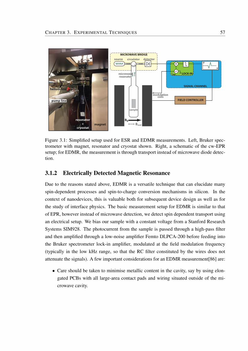
CHAPTER 3. EXPERIMENTAL TECHNIQUES 57
MICROWAVE BRIDGE
SIGNAL CHANNEL
LOCK-IN
FIELD CONTROLLER
B0Bmod
source circulator detector
microwave resonator
sample
fmod
modulation coils
x
y
magnetresonator
+cryostat
helium line
pump line
Figure 3.1: Simplified setup used for ESR and EDMR measurements. Left, Bruker spec-trometer with magnet, resonator and cryostat shown. Right, a schematic of the cw-EPRsetup; for EDMR, the measurement is through transport instead of microwave diode detec-tion.
3.1.2 Electrically Detected Magnetic Resonance
Due to the reasons stated above, EDMR is a versatile technique that can elucidate manyspin-dependent processes and spin-to-charge conversion mechanisms in silicon. In thecontext of nanodevices, this is valuable both for subsequent device design as well as forthe study of interface physics. The basic measurement setup for EDMR is similar to thatof EPR, however instead of microwave detection, we detect spin dependent transport usingan electrical setup. We bias our sample with a constant voltage from a Stanford ResearchSystems SIM928. The photocurrent from the sample is passed through a high-pass filterand then amplified through a low-noise amplifier Femto DLPCA-200 before feeding intothe Bruker spectrometer lock-in amplifier, modulated at the field modulation frequency(typically in the low kHz range, so that the RC filter constituted by the wires does notattenuate the signals). A few important considerations for an EDMR measurement[86] are:
• Care should be taken to minimise metallic content in the cavity, say by using elon-gated PCBs with all large-area contact pads and wiring situated outside of the mi-crowave cavity.
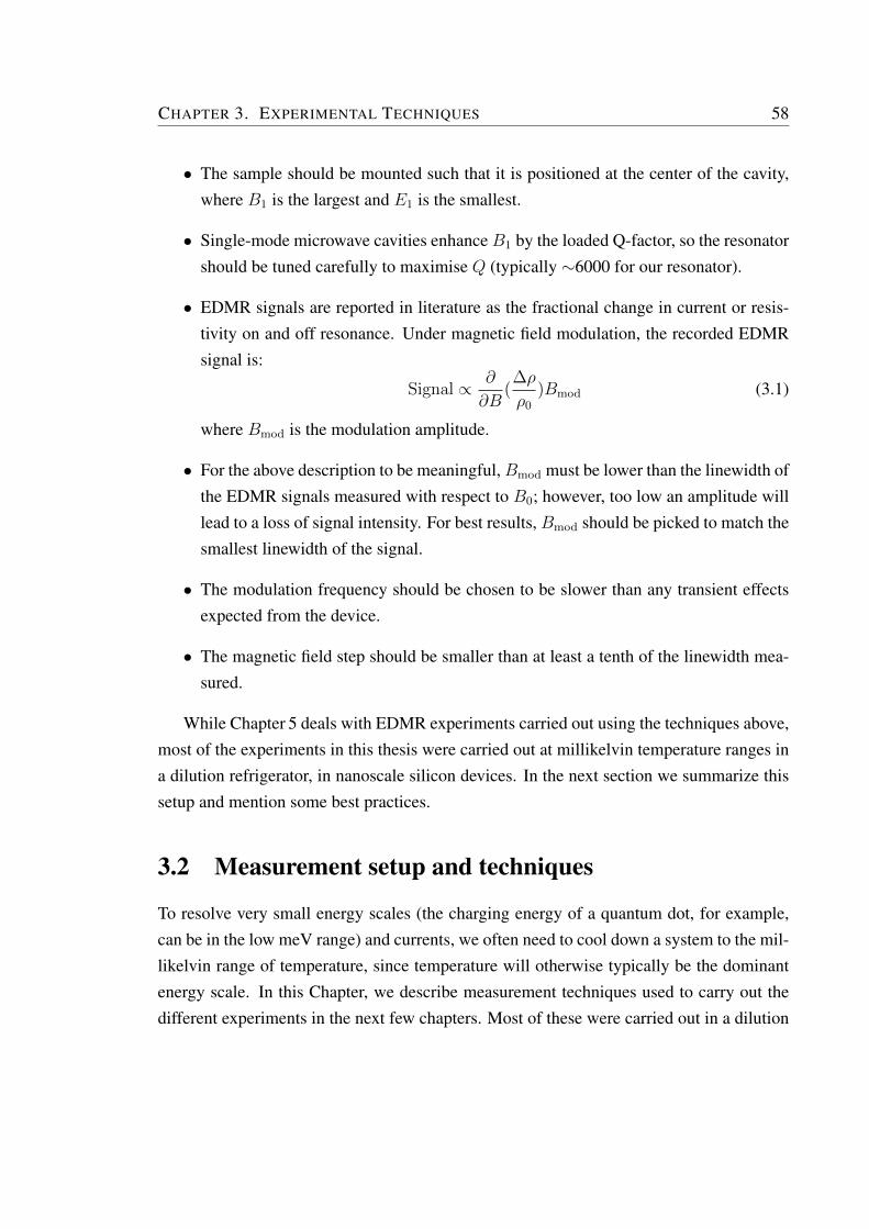
CHAPTER 3. EXPERIMENTAL TECHNIQUES 58
• The sample should be mounted such that it is positioned at the center of the cavity,where B1 is the largest and E1 is the smallest.
• Single-mode microwave cavities enhance B1 by the loaded Q-factor, so the resonatorshould be tuned carefully to maximise Q (typically ∼6000 for our resonator).
• EDMR signals are reported in literature as the fractional change in current or resis-tivity on and off resonance. Under magnetic field modulation, the recorded EDMRsignal is:
Signal ∝ ∂
∂B(∆ρ
ρ0
)Bmod (3.1)
where Bmod is the modulation amplitude.
• For the above description to be meaningful,Bmod must be lower than the linewidth ofthe EDMR signals measured with respect to B0; however, too low an amplitude willlead to a loss of signal intensity. For best results, Bmod should be picked to match thesmallest linewidth of the signal.
• The modulation frequency should be chosen to be slower than any transient effectsexpected from the device.
• The magnetic field step should be smaller than at least a tenth of the linewidth mea-sured.
While Chapter 5 deals with EDMR experiments carried out using the techniques above,most of the experiments in this thesis were carried out at millikelvin temperature ranges ina dilution refrigerator, in nanoscale silicon devices. In the next section we summarize thissetup and mention some best practices.
3.2 Measurement setup and techniques
To resolve very small energy scales (the charging energy of a quantum dot, for example,can be in the low meV range) and currents, we often need to cool down a system to the mil-likelvin range of temperature, since temperature will otherwise typically be the dominantenergy scale. In this Chapter, we describe measurement techniques used to carry out thedifferent experiments in the next few chapters. Most of these were carried out in a dilution
CHAPTER 3. EXPERIMENTAL TECHNIQUES 59
fridge, and this involved the wiring and setup of DC, pulse and microwave lines as well asan RF-reflectometry setup at milliKelvin temperatures.
To this end, several measurements described in this report were performed in a cryogen-free, top-loading Oxford Triton 200 dilution refrigerator with a stable base temperature of30 mK and with high-homogeneity and horizontal (±3T main coil, ±0-0.1T sweep coil)superconducting magnets. The rest of this section describes a few essential features of thisrefrigerator and some extended wiring and filtering work performed on it1. At all stages,effort has been taken to design a simple, plug-and-play enabled system which is easilymodifiable. The rest of the cryogenic experiments were carried out at the University ofCambridge, in a Kelvinox K400 dilution refrigerator with a base temperature of 35 mK, thewiring of which was already installed (and is described in detail elsewhere[89]).
DC lines
Equipped with 24 DC lines, our fridge has an RF reflectometry setup as well as severalstages of filtering. The filtered DC lines consist of an enmeshed copper loom with 12twisted pairs and are connected to the sample PCB (described later) via a simple plug-and-play PCI connector2 into which the PCB slots. At the mixing chamber stage, six of these 24wires are copper, chosen to apply larger currents (for example to the source and drain of thedevice under measurement), while the rest are manganin, chosen to minimize the heat loadto the mixing chamber. All wires are thermally anchored to the fridge by making thermalcontact to the fridge plates at various stages. Additionally at the mixing chamber plate, theloom is wound several times around a copper bobbin anchored to the plate, with each layerwrapped with Eccosorb3 as shown in the left panel of Fig. 3.2, to minimize radiation. TheEccosorb is also part of the filtering stages, described below.
Filtering
The DC wires extend from the device at millikelvin temperatures to the measurement elec-tronics at room temperature, so they need to be carefully filtered and heat-sinked to avoidheating up the sample (the electron temperature can be elevated due to electrical noise
1We do not describe the stages of the fridge in detail since by now such wiring is fairly standard. Thesesby Alex Johnson[87] or Leonardo Di Carlo[88] provide good methods and rationales for wiring a dilutionfridge from scratch.
2PCI Express connector, FCI 10039755.3Eccosorb microwave absorber material, LS24 0.25 inch wide absorbent foam sheet, Emerson and Cun-
ning Microwave Products Inc., available at http://www.eccosorb.com/
CHAPTER 3. EXPERIMENTAL TECHNIQUES 60
from the leads). Several stages are required at different temperatures and frequencies. Atroom temperature, the wires are connected to a fixed fridge ground through switches andembedded in a breakout box. At various stages in the fridge (50K, 4K, 800mK,100mK),Eccosorb is wrapped around the loom using nylon thread. This material is a lossy mi-crowave absorber and has been used with success in cryogenic systems for absorption ofhigh-frequency radiation (1-26 GHz). Such a stage is shown in Fig. 3.2.
Figure 3.2: Left, mixing chamber stage showing thermal anchoring of the loom (DC lines)using a copper bobbin and Eccosorb. Right, loom filtering with Eccosorb, duplicated atdifferent stages in the dilution fridge.
To get rid of further high-frequency noise, copper powder filters are utilized. These arewell-established in cryogenic systems and consist generally of powdered copper suspendedin epoxy into which the wires to be filtered are embedded. In our home-built filteringsystem, instead of a box with physical wires coiled inside and fixed inside the fridge, weutilise a PCB with 24 gold traces each 100µm wide that meander to a total length of 1.5m,covered with Stycast 1266 clear epoxy[90], connectorized inside a copper box. The epoxyhas been mixed with copper powder of 3µm average diameter. The PCB based designmakes the entire assembly plug-and-play by making use of D-connectors on both ends, andit allows us to integrate the next stage of filtering on it as well: RC filters.
To remove the remaining low frequency noise, we add RC filters to the remaining partof the wires on the PCB. This is done by soldering suface-mount resistors and capacitorsonto each line and to ground. By using replaceable SMD resistors and capacitors, we can
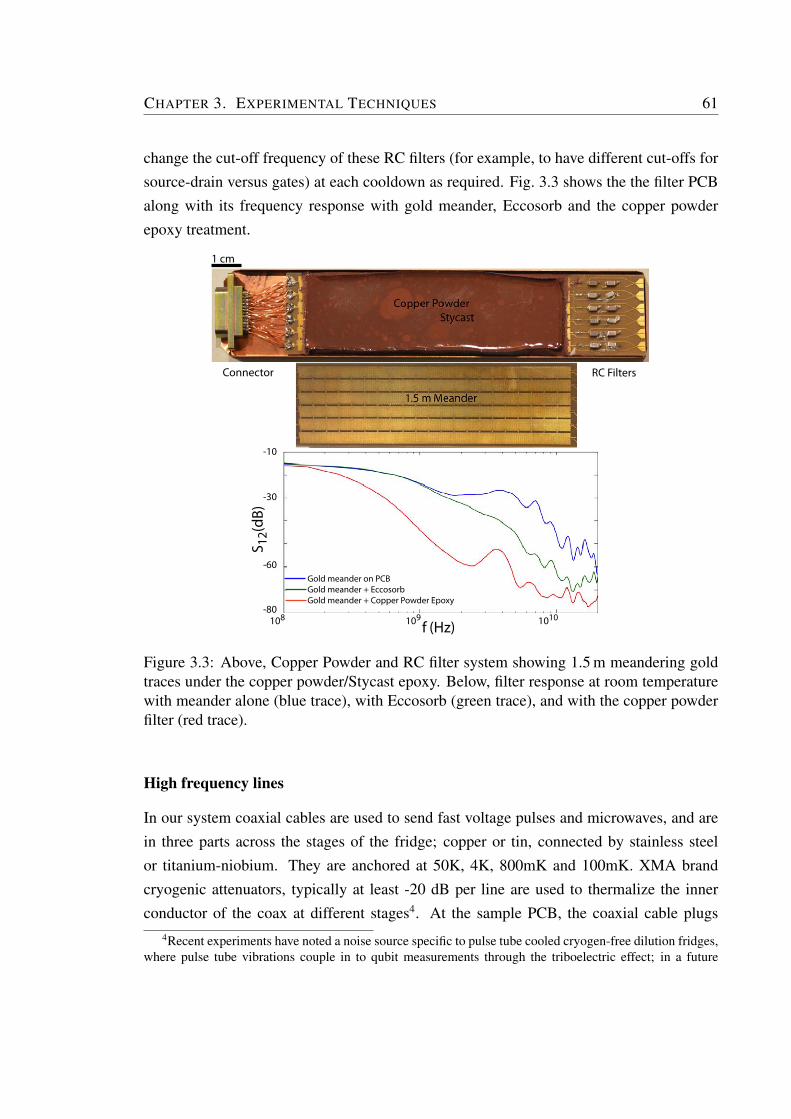
CHAPTER 3. EXPERIMENTAL TECHNIQUES 61
change the cut-off frequency of these RC filters (for example, to have different cut-offs forsource-drain versus gates) at each cooldown as required. Fig. 3.3 shows the the filter PCBalong with its frequency response with gold meander, Eccosorb and the copper powderepoxy treatment.
RC FiltersConnector
1 cm
-10
-30
-60
-80
S 12(
dB)
f (Hz)
Gold meander on PCBGold meander + EccosorbGold meander + Copper Powder Epoxy
108 109 1010
Figure 3.3: Above, Copper Powder and RC filter system showing 1.5 m meandering goldtraces under the copper powder/Stycast epoxy. Below, filter response at room temperaturewith meander alone (blue trace), with Eccosorb (green trace), and with the copper powderfilter (red trace).
High frequency lines
In our system coaxial cables are used to send fast voltage pulses and microwaves, and arein three parts across the stages of the fridge; copper or tin, connected by stainless steelor titanium-niobium. They are anchored at 50K, 4K, 800mK and 100mK. XMA brandcryogenic attenuators, typically at least -20 dB per line are used to thermalize the innerconductor of the coax at different stages4. At the sample PCB, the coaxial cable plugs
4Recent experiments have noted a noise source specific to pulse tube cooled cryogen-free dilution fridges,where pulse tube vibrations couple in to qubit measurements through the triboelectric effect; in a future
CHAPTER 3. EXPERIMENTAL TECHNIQUES 62
into an SMP connector5, which is then connected to a copper trace coated with silver fromwhich we can bond to the chip (this sample PCB is described in the next section).
Measurement PCB
For connecting the microscopic world of the device to the macroscopic world of the mea-surement system, we have developed a PCB which houses the chip and from which we canwirebond to the leads of the sample. The PCB material is Rogers 4003C laminate on FR4,(400µm wide), selected for its superior high-frequency operation and because of its similarthermal expansion coefficient to copper and its low dielectric constant which minimisesparasitic capacitance. This material lets us design low-loss high frequency traces which isimportant for our pulsed, ESR and RF lines. These traces are connected to the coaxial ca-bles via an SMP connector (mentioned above) that enables right-angled connections. Thesetraces also include slots for surface mounted inductors, capacitors and resistors which cantogether form easily replaceable bias tees as well as a tank circuit for the RF line. Viasrandomly spaced throughout the PCB connect the top and bottom ground planes and mini-mize crosstalk between lines. As mentioned before, the DC wires coming to the PCB makeconnection to the traces when the PCB is plugged into a PCI connector at one end. A silverinstead of gold finish ensures that the magnetic material nickel, often included as a layerin a gold deposition on commercial PCBs, is not present on our PCB. In a later design, acutout was added to access the back of the sample with a laser or other optical excitation,as well as a connectorized copper box encapsulating the PCB.
Dip-probe and optical access
Miscellaneous parts of the lab measurement system that have been developed include adip-probe that can used for preliminary measurements, at room temperature and at 4K inliquid helium (it can be used in either an Oxford Instruments CF-935 optical flow cryostatfor the Bruker spectrometer system, or in a helium dewar, having a system to adjust itsheight). The dip-probe has the same PCI connector as the fridge PCB, which makes thePCB usable on either system, enabling multiple samples to be tested at 4K before selectingone for cooling to dilution temperatures. Apart from this, the Oxford Triton dilution fridge
setup, cables used should be tested for such effects. In general, jacketed cables were found to have bettercharacteristics[91].
5SMP-MOLEX-73415-3320 connectors, specified up to 40 GHz.
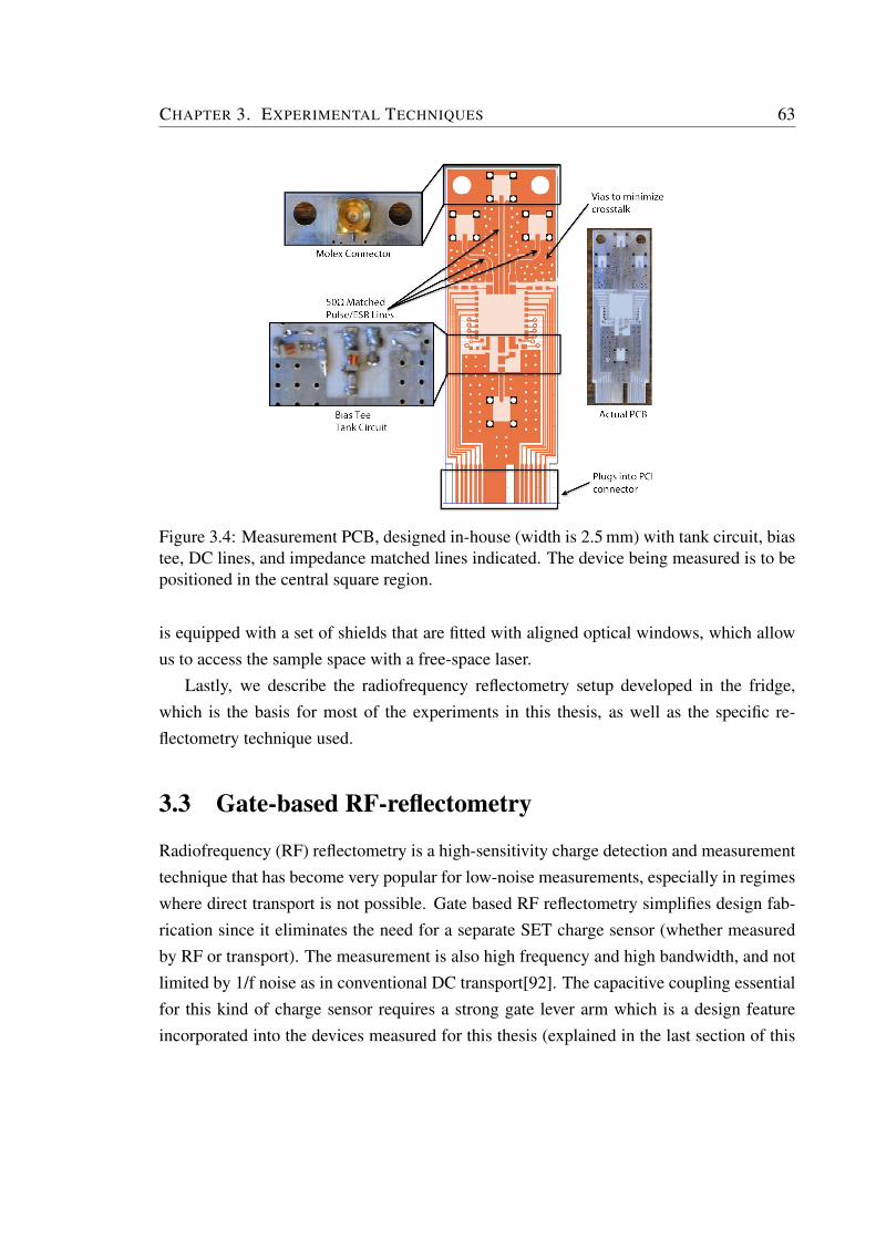
CHAPTER 3. EXPERIMENTAL TECHNIQUES 63
Figure 3.4: Measurement PCB, designed in-house (width is 2.5 mm) with tank circuit, biastee, DC lines, and impedance matched lines indicated. The device being measured is to bepositioned in the central square region.
is equipped with a set of shields that are fitted with aligned optical windows, which allowus to access the sample space with a free-space laser.
Lastly, we describe the radiofrequency reflectometry setup developed in the fridge,which is the basis for most of the experiments in this thesis, as well as the specific re-flectometry technique used.
3.3 Gate-based RF-reflectometry
Radiofrequency (RF) reflectometry is a high-sensitivity charge detection and measurementtechnique that has become very popular for low-noise measurements, especially in regimeswhere direct transport is not possible. Gate based RF reflectometry simplifies design fab-rication since it eliminates the need for a separate SET charge sensor (whether measuredby RF or transport). The measurement is also high frequency and high bandwidth, and notlimited by 1/f noise as in conventional DC transport[92]. The capacitive coupling essentialfor this kind of charge sensor requires a strong gate lever arm which is a design featureincorporated into the devices measured for this thesis (explained in the last section of this
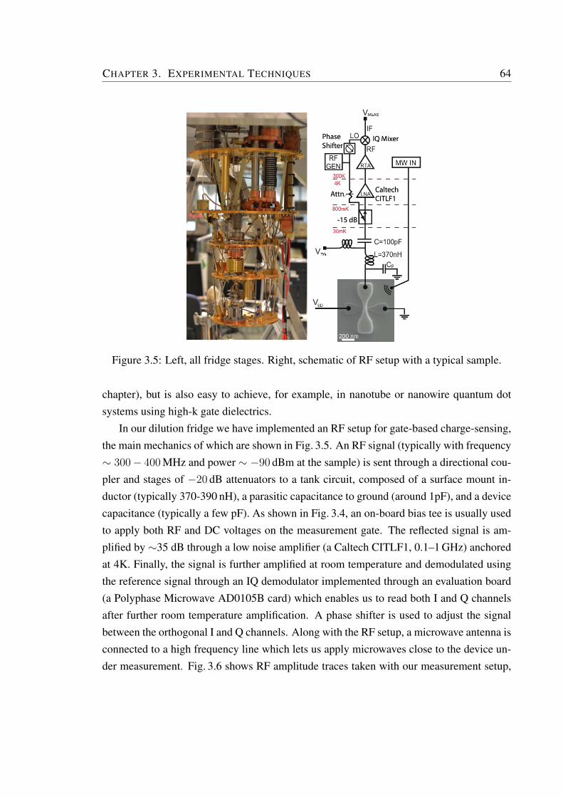
CHAPTER 3. EXPERIMENTAL TECHNIQUES 64
Figure 3.5: Left, all fridge stages. Right, schematic of RF setup with a typical sample.
chapter), but is also easy to achieve, for example, in nanotube or nanowire quantum dotsystems using high-k gate dielectrics.
In our dilution fridge we have implemented an RF setup for gate-based charge-sensing,the main mechanics of which are shown in Fig. 3.5. An RF signal (typically with frequency∼ 300− 400 MHz and power ∼ −90 dBm at the sample) is sent through a directional cou-pler and stages of −20 dB attenuators to a tank circuit, composed of a surface mount in-ductor (typically 370-390 nH), a parasitic capacitance to ground (around 1pF), and a devicecapacitance (typically a few pF). As shown in Fig. 3.4, an on-board bias tee is usually usedto apply both RF and DC voltages on the measurement gate. The reflected signal is am-plified by ∼35 dB through a low noise amplifier (a Caltech CITLF1, 0.1–1 GHz) anchoredat 4K. Finally, the signal is further amplified at room temperature and demodulated usingthe reference signal through an IQ demodulator implemented through an evaluation board(a Polyphase Microwave AD0105B card) which enables us to read both I and Q channelsafter further room temperature amplification. A phase shifter is used to adjust the signalbetween the orthogonal I and Q channels. Along with the RF setup, a microwave antenna isconnected to a high frequency line which lets us apply microwaves close to the device un-der measurement. Fig. 3.6 shows RF amplitude traces taken with our measurement setup,
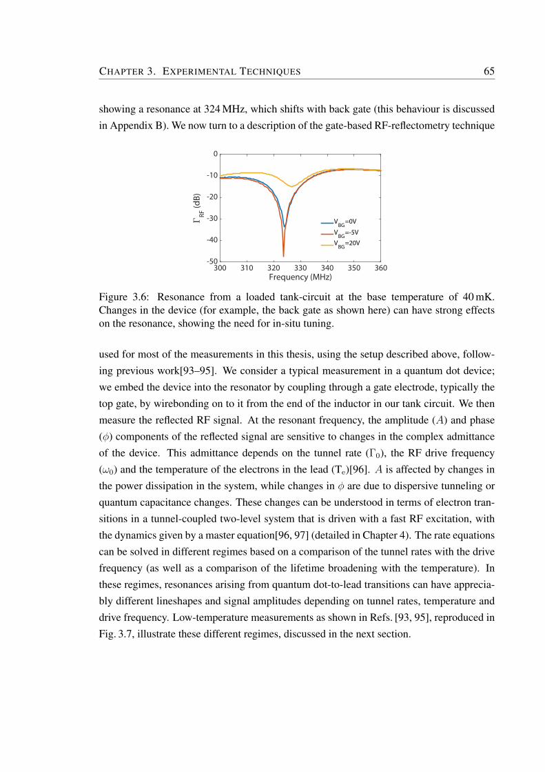
CHAPTER 3. EXPERIMENTAL TECHNIQUES 65
showing a resonance at 324 MHz, which shifts with back gate (this behaviour is discussedin Appendix B). We now turn to a description of the gate-based RF-reflectometry technique
Figure 3.6: Resonance from a loaded tank-circuit at the base temperature of 40 mK.Changes in the device (for example, the back gate as shown here) can have strong effectson the resonance, showing the need for in-situ tuning.
used for most of the measurements in this thesis, using the setup described above, follow-ing previous work[93–95]. We consider a typical measurement in a quantum dot device;we embed the device into the resonator by coupling through a gate electrode, typically thetop gate, by wirebonding on to it from the end of the inductor in our tank circuit. We thenmeasure the reflected RF signal. At the resonant frequency, the amplitude (A) and phase(φ) components of the reflected signal are sensitive to changes in the complex admittanceof the device. This admittance depends on the tunnel rate (Γ0), the RF drive frequency(ω0) and the temperature of the electrons in the lead (Te)[96]. A is affected by changes inthe power dissipation in the system, while changes in φ are due to dispersive tunneling orquantum capacitance changes. These changes can be understood in terms of electron tran-sitions in a tunnel-coupled two-level system that is driven with a fast RF excitation, withthe dynamics given by a master equation[96, 97] (detailed in Chapter 4). The rate equationscan be solved in different regimes based on a comparison of the tunnel rates with the drivefrequency (as well as a comparison of the lifetime broadening with the temperature). Inthese regimes, resonances arising from quantum dot-to-lead transitions can have apprecia-bly different lineshapes and signal amplitudes depending on tunnel rates, temperature anddrive frequency. Low-temperature measurements as shown in Refs. [93, 95], reproduced inFig. 3.7, illustrate these different regimes, discussed in the next section.
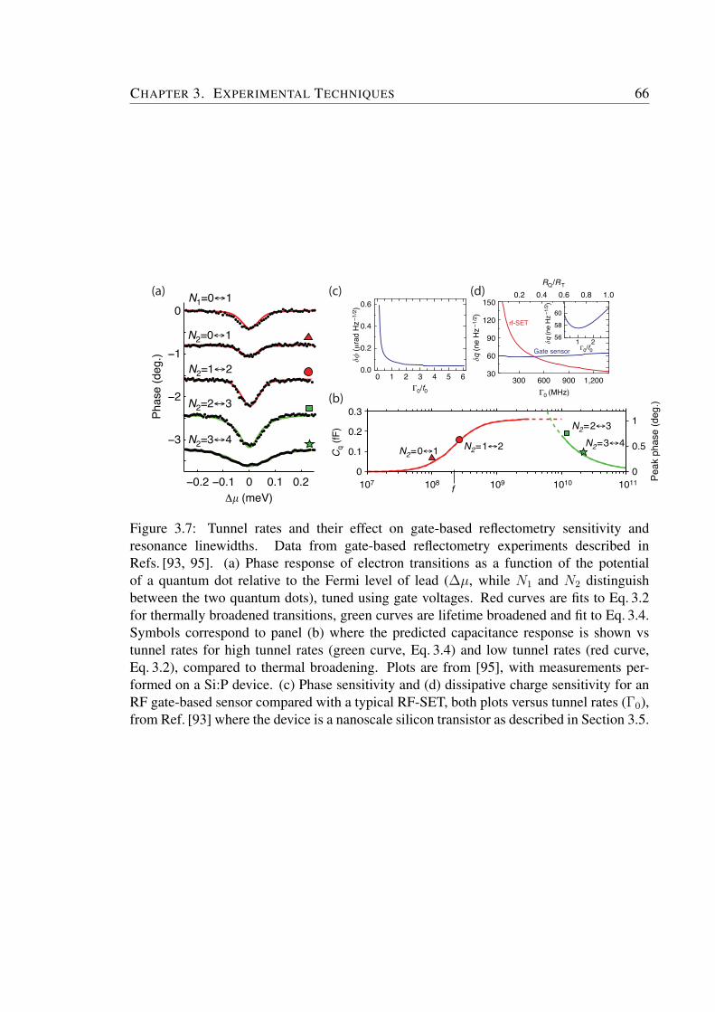
CHAPTER 3. EXPERIMENTAL TECHNIQUES 66
−0.2 −0.1 0 0.1 0.2
−3
−2
−1
0
Phas
e (d
eg.)
N1=0↔1
N2=0↔1
N2=2↔3
N2=3↔4
N2=1↔2
Δ (meV)107 108 109 1010 1011
0
0.1
0.2
0.3
0
0.5
1
Peak
pha
se (d
eg.)
N2=3↔4N2=2↔3
N2=1↔2N2=0↔1
f
Cq (
fF)
Γ0/f0
(μra
d H
z–1/
2 )
0.00 1 2 3 4 5 6
0.2
0.4
0.6
Gate sensor
rf-SET
q (n
e H
z–1/
2 )
q (n
e H
z–1/2
)
Γ0 (MHz)
Γ0/f0
RQ/R T
30300
0.2 0.4
60
58
56 1 2
0.6 0.8 1.0
600 900 1,200
60
90
120
150(a) (c)
(b)
(d)
Figure 3.7: Tunnel rates and their effect on gate-based reflectometry sensitivity andresonance linewidths. Data from gate-based reflectometry experiments described inRefs. [93, 95]. (a) Phase response of electron transitions as a function of the potentialof a quantum dot relative to the Fermi level of lead (∆µ, while N1 and N2 distinguishbetween the two quantum dots), tuned using gate voltages. Red curves are fits to Eq. 3.2for thermally broadened transitions, green curves are lifetime broadened and fit to Eq. 3.4.Symbols correspond to panel (b) where the predicted capacitance response is shown vstunnel rates for high tunnel rates (green curve, Eq. 3.4) and low tunnel rates (red curve,Eq. 3.2), compared to thermal broadening. Plots are from [95], with measurements per-formed on a Si:P device. (c) Phase sensitivity and (d) dissipative charge sensitivity for anRF gate-based sensor compared with a typical RF-SET, both plots versus tunnel rates (Γ0),from Ref. [93] where the device is a nanoscale silicon transistor as described in Section 3.5.
CHAPTER 3. EXPERIMENTAL TECHNIQUES 67
3.3.1 Detection regimes based on tunnel rates
Considering the case of a quantum dot coupled to a lead, the RF reflectometry signal typ-ically shows a peak at the degeneracy point in the dissipative and dispersive responses aswe tune the two levels. However, we need to look at traces taken well away from anytriple-point charge degeneracies to avoid cotunneling effects.
Low tunnel rates
At low tunnel rates, i.e. kBTe ~Γ0 the width of the transitions is determined by theelectron temperature since the thermal energy is greater than the lifetime broadening dueto the interaction with the leads. The rate equations then give us the following relations forthe average power dissipation in the device (P ) and the averaged phase response (φ):
〈P 〉 ≈(eV rf
g α)2
4kBTe
cosh−2(∆E(0)
2kBTe
)Γ0
1 + Γ20/ω
20
(3.2)
〈φ〉 ≈ −πQCp
(eα)2
4kBTe
cosh−2(∆E(0)
2kBTe
)1
1 + ω20/Γ
20
(3.3)
with V rfg the gate voltage change produced by the RF-drive, and ∆E(0) the energy sepa-
ration of the two level system at zero detuning. A few things to be noted about this regimeare, firstly, that at low tunnel rates, the peak quantum capacitance is low, and no additionalpower is dissipated in the device, since electron tunneling cannot keep up with the drive.Secondly, we note that the peak at the degeneracy point has a cosh−2 dependence, borneout by the experimental results shown in Fig. 3.7. The width of this peak gives us thethermal energy and therefore the electron temperature. Lastly, as seen in Fig. 3.7(c)-(d),Ref. [93] measured the charge sensitivity of this technique and found a very low value of37µe Hz−1/2, outdone only by RF-SETs (1µe Hz−1/2), which perform best at high tunnelrates (>600 MHz), while the gate based sensor performs well in all regimes, including bet-ter than RF-SETs at low tunnel rates <500 MHz). Low tunnel rates correspond to highlyresistive tunnel barriers, which is usually the situation for few-electron quantum dots.
Tunnel rates comparable to drive frequency
For Γ0 ∼ ω0, we find that maximum power is dissipated since on average, inelastic tunnel-ing happens at the end of the RF cycle, and inelastic tunneling results in an excess dissipated
CHAPTER 3. EXPERIMENTAL TECHNIQUES 68
energy which results in a change in the total reflected power. Significant dissipation is notideal as it introduces noise into the measurement, but the maximum charge sensitivity ofthe RF-resonator is also seen when the tunnel rate matches the drive frequency.
However, an encouraging consequence of the above relations is that unlike the powerdissipation, the average phase response does not peak at the resonant frequency and thendrop again, but goes to a constant value for large Γ0. In this limit, the excess power dissi-pation can be minimised while the phase response is still maximised.
High tunnel rates
If the tunnel rates are considerably faster than the drive frequency, i.e. Γ0 > ω0, thecoupling is capacitive only and electron tunneling occurs out of phase with the drivingsignal. Electron tunneling is elastic and power dissipation does not occur. In this regime ofdispersive readout the parametric capacitance response Cp can be given by
Cp ≈(αV rf
g e)2
π
~Γ0
(~Γ0)2 + (∆E)2(3.4)
In this regime, the width of the peak, when fit to the above equation, gives the lifetimebroadening, i.e. the tunnel rates. Phase detection is maximised at these tunnel rates, aregime more suitable for systems with transparent tunnel barriers (but performs well atmoderate tunnel rates as well). Fig. 3.7(a)-(b) show the predicted change in the phaseresponse and the measured resonance linewidth as the tunnel rates change.
In general, from the above regimes we learn that gate-based reflectometry works formost regimes, but tunnel rates high enough (compared to the drive frequency) to avoidmaximum dissipation but low enough to keep tunnel barriers opaque enough for measure-ment are optimum for quantum dot measurements. Tuning of the tunnel barriers can beachieved typically by barrier gates, or by back gating in the devices described later in thisthesis. The resonator frequency can of course also be tuned within a certain range by asuitable choice of components, as well as in situ using tunable inductors or varactors[98].
3.4 Fabrication of nanoscale silicon devices
We present here the design and fabrication of planar-MOS devices on a purpose-built ver-satile fabrication platform based on silicon. Silicon MOS technology is ubiquitous in con-
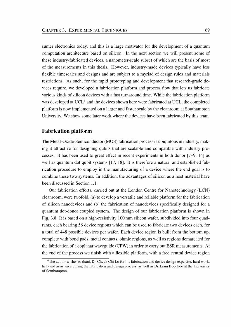
CHAPTER 3. EXPERIMENTAL TECHNIQUES 69
sumer electronics today, and this is a large motivator for the development of a quantumcomputation architecture based on silicon. In the next section we will present some ofthese industry-fabricated devices, a nanometer-scale subset of which are the basis of mostof the measurements in this thesis. However, industry-made devices typically have lessflexible timescales and designs and are subject to a myriad of design rules and materialsrestrictions. As such, for the rapid prototyping and development that research-grade de-vices require, we developed a fabrication platform and process flow that lets us fabricatevarious kinds of silicon devices with a fast turnaround time. While the fabrication platformwas developed at UCL6 and the devices shown here were fabricated at UCL, the completedplatform is now implemented on a larger and faster scale by the cleanroom at SouthamptonUniversity. We show some later work where the devices have been fabricated by this team.
Fabrication platform
The Metal-Oxide-Semiconductor (MOS) fabrication process is ubiquitous in industry, mak-ing it attractive for designing qubits that are scalable and compatible with industry pro-cesses. It has been used to great effect in recent experiments in both donor [7–9, 14] aswell as quantum dot qubit systems [17, 18]. It is therefore a natural and established fab-rication procedure to employ in the manufacturing of a device where the end goal is tocombine these two systems. In addition, the advantages of silicon as a host material havebeen discussed in Section 1.1.
Our fabrication efforts, carried out at the London Centre for Nanotechnology (LCN)cleanroom, were twofold, (a) to develop a versatile and reliable platform for the fabricationof silicon nanodevices and (b) the fabrication of nanodevices specifically designed for aquantum dot-donor coupled system. The design of our fabrication platform is shown inFig. 3.8. It is based on a high-resistivity 100 mm silicon wafer, subdivided into four quad-rants, each bearing 56 device regions which can be used to fabricate two devices each, fora total of 448 possible devices per wafer. Each device region is built from the bottom up,complete with bond pads, metal contacts, ohmic regions, as well as regions demarcated forthe fabrication of a coplanar waveguide (CPW) in order to carry out ESR measurements. Atthe end of the process we finish with a flexible platform, with a free central device region
6The author wishes to thank Dr. Cheuk Chi Lo for his fabrication and device design expertise, hard work,help and assistance during the fabrication and design process, as well as Dr. Liam Boodhoo at the Universityof Southampton.
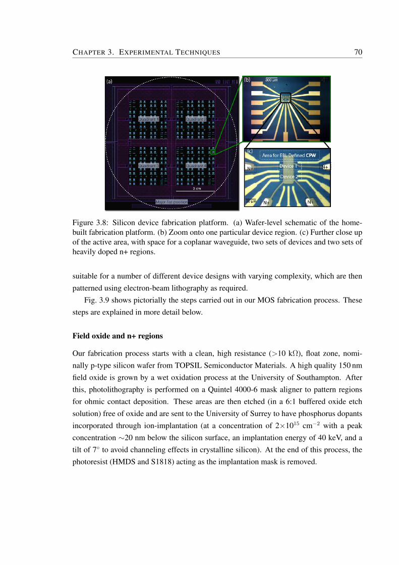
CHAPTER 3. EXPERIMENTAL TECHNIQUES 70
Figure 3.8: Silicon device fabrication platform. (a) Wafer-level schematic of the home-built fabrication platform. (b) Zoom onto one particular device region. (c) Further close upof the active area, with space for a coplanar waveguide, two sets of devices and two sets ofheavily doped n+ regions.
suitable for a number of different device designs with varying complexity, which are thenpatterned using electron-beam lithography as required.
Fig. 3.9 shows pictorially the steps carried out in our MOS fabrication process. Thesesteps are explained in more detail below.
Field oxide and n+ regions
Our fabrication process starts with a clean, high resistance (>10 kΩ), float zone, nomi-nally p-type silicon wafer from TOPSIL Semiconductor Materials. A high quality 150 nmfield oxide is grown by a wet oxidation process at the University of Southampton. Afterthis, photolithography is performed on a Quintel 4000-6 mask aligner to pattern regionsfor ohmic contact deposition. These areas are then etched (in a 6:1 buffered oxide etchsolution) free of oxide and are sent to the University of Surrey to have phosphorus dopantsincorporated through ion-implantation (at a concentration of 2×1015 cm−2 with a peakconcentration ∼20 nm below the silicon surface, an implantation energy of 40 keV, and atilt of 7 to avoid channeling effects in crystalline silicon). At the end of this process, thephotoresist (HMDS and S1818) acting as the implantation mask is removed.
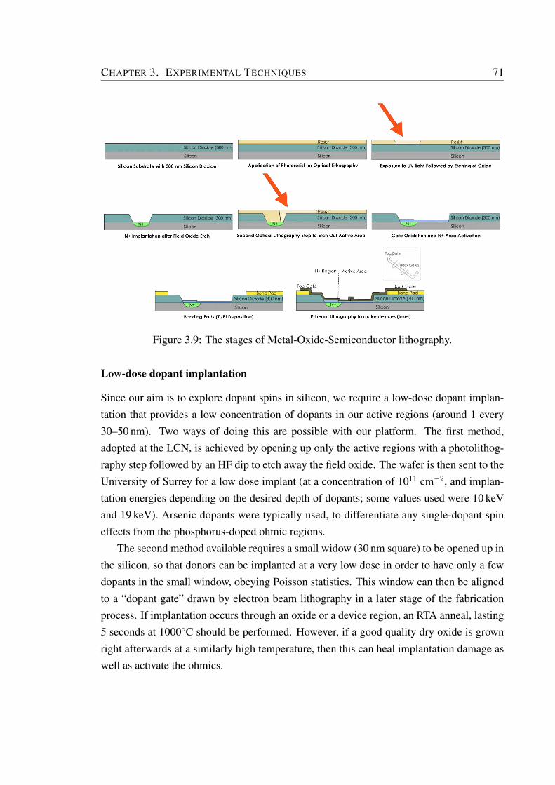
CHAPTER 3. EXPERIMENTAL TECHNIQUES 71
Figure 3.9: The stages of Metal-Oxide-Semiconductor lithography.
Low-dose dopant implantation
Since our aim is to explore dopant spins in silicon, we require a low-dose dopant implan-tation that provides a low concentration of dopants in our active regions (around 1 every30–50 nm). Two ways of doing this are possible with our platform. The first method,adopted at the LCN, is achieved by opening up only the active regions with a photolithog-raphy step followed by an HF dip to etch away the field oxide. The wafer is then sent to theUniversity of Surrey for a low dose implant (at a concentration of 1011 cm−2, and implan-tation energies depending on the desired depth of dopants; some values used were 10 keVand 19 keV). Arsenic dopants were typically used, to differentiate any single-dopant spineffects from the phosphorus-doped ohmic regions.
The second method available requires a small widow (30 nm square) to be opened up inthe silicon, so that donors can be implanted at a very low dose in order to have only a fewdopants in the small window, obeying Poisson statistics. This window can then be alignedto a “dopant gate” drawn by electron beam lithography in a later stage of the fabricationprocess. If implantation occurs through an oxide or a device region, an RTA anneal, lasting5 seconds at 1000C should be performed. However, if a good quality dry oxide is grownright afterwards at a similarly high temperature, then this can heal implantation damage aswell as activate the ohmics.
CHAPTER 3. EXPERIMENTAL TECHNIQUES 72
Device regions and gate oxide
The active regions of the device are now etched free of field oxide, using another pho-tolithography step, followed by another field oxide etch (this will already have been done ifthe low dose implant is performed at this stage). The active regions are now bare silicon. Ahigh quality 9 nm gate oxide is then grown at the University of Southampton (14 minutesof dry oxidation at 900C, followed by a 20 minute nitrogen anneal at 950C). This alsohas the effect of activating the n+ regions.
Metal contact and bond pad deposition
A third photolithography step is used to deposit aluminium metal contacts through thermalevaporation after etching of the thin oxide. A fourth, and final, photolithography step isused to define alignment marks, device numbering, as well as the large-feature bond padswhich will be used to contact the device for measurement. These are deposited by electronbeam evaporation and are composed of 8 nm titanium as a sticking layer, followed by∼45 nm platinum for visibility under the electron-beam system. The wafer is now readyto be diced into smaller, manageable pieces that are ideal for the smaller-scale precisionelectron beam lithography to produce a nanoscale device.
Device lithography
Electron beam lithography (EBL) is well-suited to devices at this scale since using an elec-tron beam enables us to overcome the diffraction limit of light, allowing the writing of verysmall features (of the order of 20–30 nm). We use a Raith 150-TWO EBL tool to writefeatures of the order of tens of nanometers, with a minimum feature size of 30 nm and apitch of 30 nm achieved. The sample is spin-coated with a ∼100 nm thick layer of the pos-itive resist polymethyl-methacrylate (PMMA) 950 A2. A typical exposure is at a small (10micron) aperture and a 20 kV excitation voltage. After exposure, the sample is developed;the exposed PMMA is dissolved and metal deposition through thermal evaporation is car-ried out, followed by an overnight liftoff immersion in the solvent acetone. This is usuallyfollowed by a second device layer, made up of the top gate and a coplanar waveguide forqubit control. Between layers, the aluminium gates are passivated by oxidation; a ∼3 nmthick aluminium oxide is grown on a hot plate at 150C for 10 minutes in the cleanroomatmosphere. This process may be repeated multiple times for different device layers in thedesign, however the ultimate gate stack height is limited by the thickness of the resist since
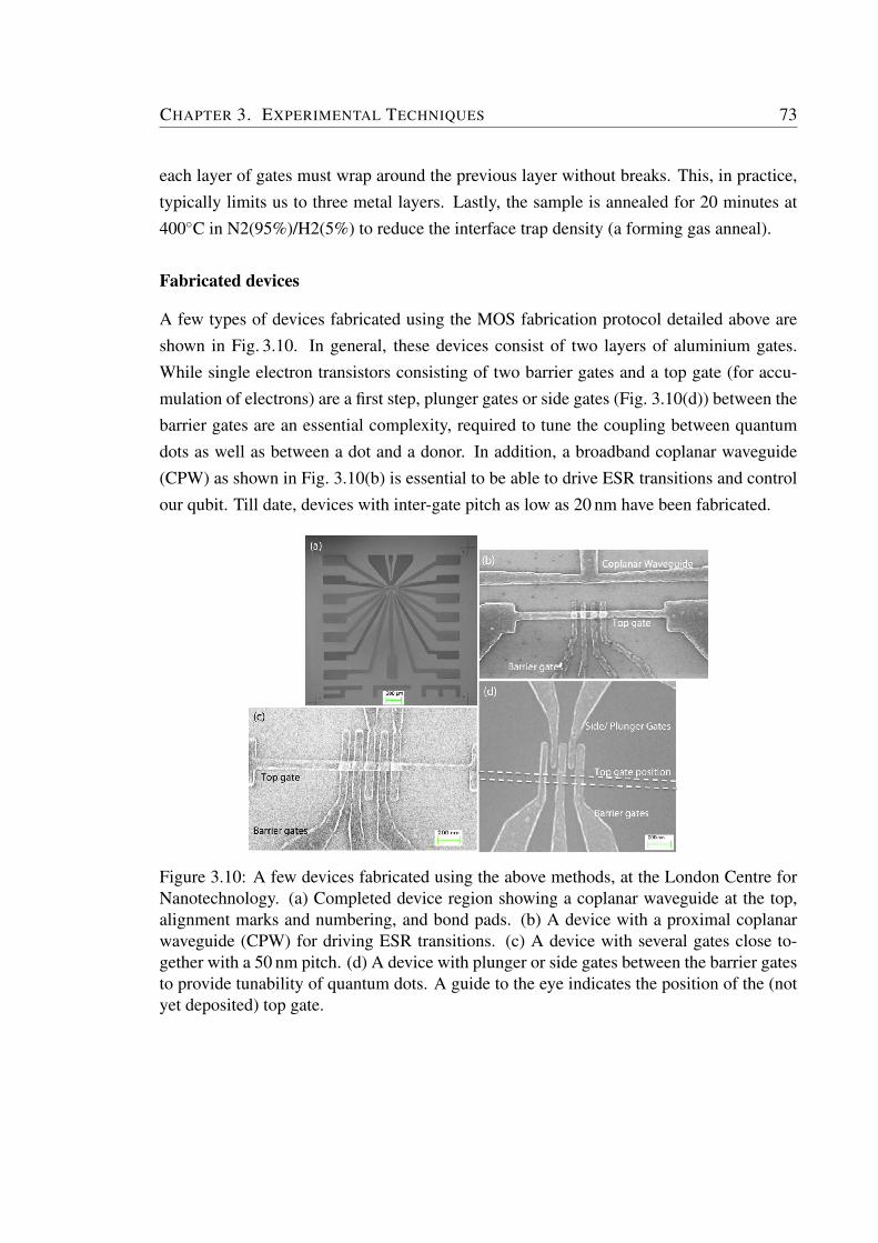
CHAPTER 3. EXPERIMENTAL TECHNIQUES 73
each layer of gates must wrap around the previous layer without breaks. This, in practice,typically limits us to three metal layers. Lastly, the sample is annealed for 20 minutes at400C in N2(95%)/H2(5%) to reduce the interface trap density (a forming gas anneal).
Fabricated devices
A few types of devices fabricated using the MOS fabrication protocol detailed above areshown in Fig. 3.10. In general, these devices consist of two layers of aluminium gates.While single electron transistors consisting of two barrier gates and a top gate (for accu-mulation of electrons) are a first step, plunger gates or side gates (Fig. 3.10(d)) between thebarrier gates are an essential complexity, required to tune the coupling between quantumdots as well as between a dot and a donor. In addition, a broadband coplanar waveguide(CPW) as shown in Fig. 3.10(b) is essential to be able to drive ESR transitions and controlour qubit. Till date, devices with inter-gate pitch as low as 20 nm have been fabricated.
Figure 3.10: A few devices fabricated using the above methods, at the London Centre forNanotechnology. (a) Completed device region showing a coplanar waveguide at the top,alignment marks and numbering, and bond pads. (b) A device with a proximal coplanarwaveguide (CPW) for driving ESR transitions. (c) A device with several gates close to-gether with a 50 nm pitch. (d) A device with plunger or side gates between the barrier gatesto provide tunability of quantum dots. A guide to the eye indicates the position of the (notyet deposited) top gate.
CHAPTER 3. EXPERIMENTAL TECHNIQUES 74
Test structures
A final yet crucial component of our fabrication platform is the extensive set of test struc-tures, present at two opposite corners of every quadrant. Our test structures take up eightdevice regions per quadrant, but are nevertheless essential to the successful fabrication ofnanoscale silicon devices. Similarly to GaAs and SiGe heterostructures, where the qualityof the heterostructure is possibly the single most important factor in making a few-electronquantum dot, in silicon a high quality interface is key to making nanodevices7. To this end,testing the contact resistances, device-to-device leakage, ohmic resistivity, field oxide and(most crucially) gate oxide quality is extremely important before proceeding to the nextstep; this can save extensive amounts of time.
Some crucial parts of our test structure set are shown in Table 3.1.Measurements carried out on these structures include assessing the quality of the oxide
(both field and gate) through CV measurements, as well as standard MOSFET measure-ments (Id-Vd and Id-Vg) to gauge the quality of the ohmics, the effect of oxide qualityon transport, and device-to-device leakage. These measurements were carried out at roomtemperature and at 4K, using a Keithley Parameter Analyser connected to a cryogenic probestation, as well as in a dip-probe immersed in liquid helium after wirebonding. These mea-surements are routine and integrated into the fabrication cycle for fast feedback and processevolution.
3.4.1 Device measurements and nanofabrication challenges
Preliminary measurements on nanoscale devices were promising. The devices measuredin this section are single-electron transistors (SETs) that can potentially be used to detectsingle donors in the globally doped silicon[7]. In addition, the formation of a quantumdot in these devices would also enable exchange coupling and/or electron transfer betweensuch a single donor and the quantum dot.
At 4 K as well as in the dilution refrigerator at 30 mK, our MOS devices consistentlyshow turn on and pinch-off behaviours. Measurements on one such device, similar toFig. 3.10(b,c), are shown below in Fig. 3.11(a). The device turns on with a thresholdaround 0.6 V. Additionally, setting the top gate to above turn-on, at 0.7 V, we can use thebottom gates (separated from the top gate via the gate oxide of around 10 nm) to pinchoff the channel, either singly or together (in which case the pinch off voltage is higher).
7As Herbert Kroemer famously said, “the interface is the device”.
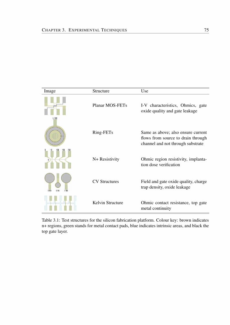
CHAPTER 3. EXPERIMENTAL TECHNIQUES 75
Image Structure Use
Planar MOS-FETs I-V characteristics, Ohmics, gateoxide quality and gate leakage
Ring-FETs Same as above; also ensure currentflows from source to drain throughchannel and not through substrate
N+ Resistivity Ohmic region resistivity, implanta-tion dose verification
CV Structures Field and gate oxide quality, chargetrap density, oxide leakage
Kelvin Structure Ohmic contact resistance, top gatemetal continuity
Table 3.1: Test structures for the silicon fabrication platform. Colour key: brown indicatesn+ regions, green stands for metal contact pads, blue indicates intrinsic areas, and black thetop gate layer.
CHAPTER 3. EXPERIMENTAL TECHNIQUES 76
Fig. 3.11(a) also shows the current in the channel near the threshold, showing Coulomboscillations.
However, a few challenges were encountered in the quest to reach the few-electronquantum dot limit.
• Oxide quality The minimisation of leakage and the optimization of oxide qualityis essential for silicon devices. Poor oxides lead to scattering and parasitic dot for-mation in transport, as well as charge fluctuations causing switching and unstabledevice behaviour during measurements. Typical defects affecting device behaviourare fixed oxide charges (surface defects created during oxide that lead to scatter-ing), interface trapped charge (silicon dangling bonds or Pb centers, oxidation orimplantation-induced), oxide trapped charges (holes or electrons trapped in the ox-ide, can be annealed out at low temperatures), and mobile ionic charges (alkali ionssuch as sodium and potassium; these can be minimised by clean processing, and deepcleaning of furnace tubes and beakers in chlorine)[99–101]. A variety of these issueswere encountered, exacerbated by the difficulty of ensuring furnace tubes clean tosilicon-grade in a university cleanroom with multiple ongoing research projects.
• Device-to-device leakage Mobile charges as well as large trap densities were foundto randomly occur in some wafers, due to the same communal processing issues asabove. These caused a common problem in silicon MOS device fabrication, that ofdevice-to-device leakage, where current flows under bias between the ohmic regionsof different devices, which are (or should be) separated by intrinsic silicon.
• Channel stoppers To neutralise the problem of device-to-device leakage after per-forming extensive simulations[102], channel stopper implants were introduced at thebeginning of the process, before the ohmic implantation step. For these, boron (at aconcentration of 1017 cm−3 about 74 nm below the surface) is implanted into a framearound the device regions to prevent current flowing between them.
• Device dimensions While substrates exhibiting good gate oxide quality and minimalleakage through the gate oxide were fabricated at the LCN, in nanodevices that weremeasured (e.g. the one shown in Fig. 3.11(a)) we were unable to reach the few-electron quantum dot regime. The high effective mass of silicon implies that to createa comparable confinement to successful GaAs quantum dot designs, the electronbeam pattern would need to be scaled down by a factor of 1.73-2.5[52]. This is at
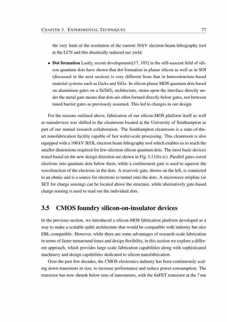
CHAPTER 3. EXPERIMENTAL TECHNIQUES 77
the very limit of the resolution of the current 30 kV electron-beam-lithography toolat the LCN and this drastically reduced our yield.
• Dot formation Lastly, recent developments[17, 103] in the still-nascent field of sili-con quantum dots have shown that dot formation in planar silicon as well as in SOI(discussed in the next section) is very different from that in heterostructure-basedmaterial systems such as GaAs and SiGe. In silicon planar MOS quantum dots basedon aluminium gates on a Si/SiO2 architecture, strain upon the interface directly un-der the metal gate means that dots are often formed directly below gates, not betweentuned barrier gates as previously assumed. This led to changes in our design.
For the reasons outlined above, fabrication of our silicon-MOS platform itself as wellas nanodevices was shifted to the cleanroom located at the University of Southampton aspart of our mutual research collaboration. The Southampton cleanroom is a state-of-the-art nanofabrication facility capable of fast wafer-scale processing. This cleanroom is alsoequipped with a 100 kV JEOL electron beam lithography tool which enables us to reach thesmaller dimensions required for few-electron silicon quantum dots. The most basic devicestested based on the new design direction are shown in Fig. 3.11(b)-(c). Parallel gates corralelectrons into quantum dots below them, while a confinement gate is used to squeeze thewavefunction of the electrons in the dots. A reservoir gate, shown on the left, is connectedto an ohmic and is a source for electrons to tunnel onto the dots. A microwave stripline (orSET for charge sensing) can be located above the structure, while alternatively gate-basedcharge sensing is used to read out the individual dots.
3.5 CMOS foundry silicon-on-insulator devices
In the previous section, we introduced a silicon-MOS fabrication platform developed as away to make a scalable qubit architecture that would be compatible with industry but alsoEBL-compatible. However, while there are some advantages of research-scale fabricationin terms of faster turnaround times and design flexibility, in this section we explore a differ-ent approach, which provides large-scale fabrication capabilities along with sophisticatedmachinery and design capabilities dedicated to silicon nanofabrication.
Over the past few decades, the CMOS electronics industry has been continuously scal-ing down transistors in size, to increase performance and reduce power consumption. Thetransistor has now shrunk below tens of nanometers, with the finFET transistor at the 7 nm
CHAPTER 3. EXPERIMENTAL TECHNIQUES 78
Gate Voltage (V)0.2 0.4 0.6 0.8 1 1.2 1.4
dI/d
V (μ
S)
0
0.5
1
1.5
2
BarrierGates On
Barrier Gates O
CPW
ConnementGate
DotGate
DotGate
Reservoir
(a)
(b) (c)CPW
Dopant Gate
Top Gate
Barrier Gates100 nm100 nm
Gate Voltage (V)
dI/d
V (μ
S)
Figure 3.11: Device tests and design progression. (a) Device near turn on showing repro-ducible conductance oscillations. Inset shows that channel can be pinched off using barriergates. Measurements taken at 30 mK on a device fabricated at the London Centre for Nan-otechology, as shown in Fig. 3.10(b, c). (b) Double quantum dot design, with dot formationexpected under each gate. (c) Dopant-dot device design, requiring local implantation of adopant under the dopant gate.
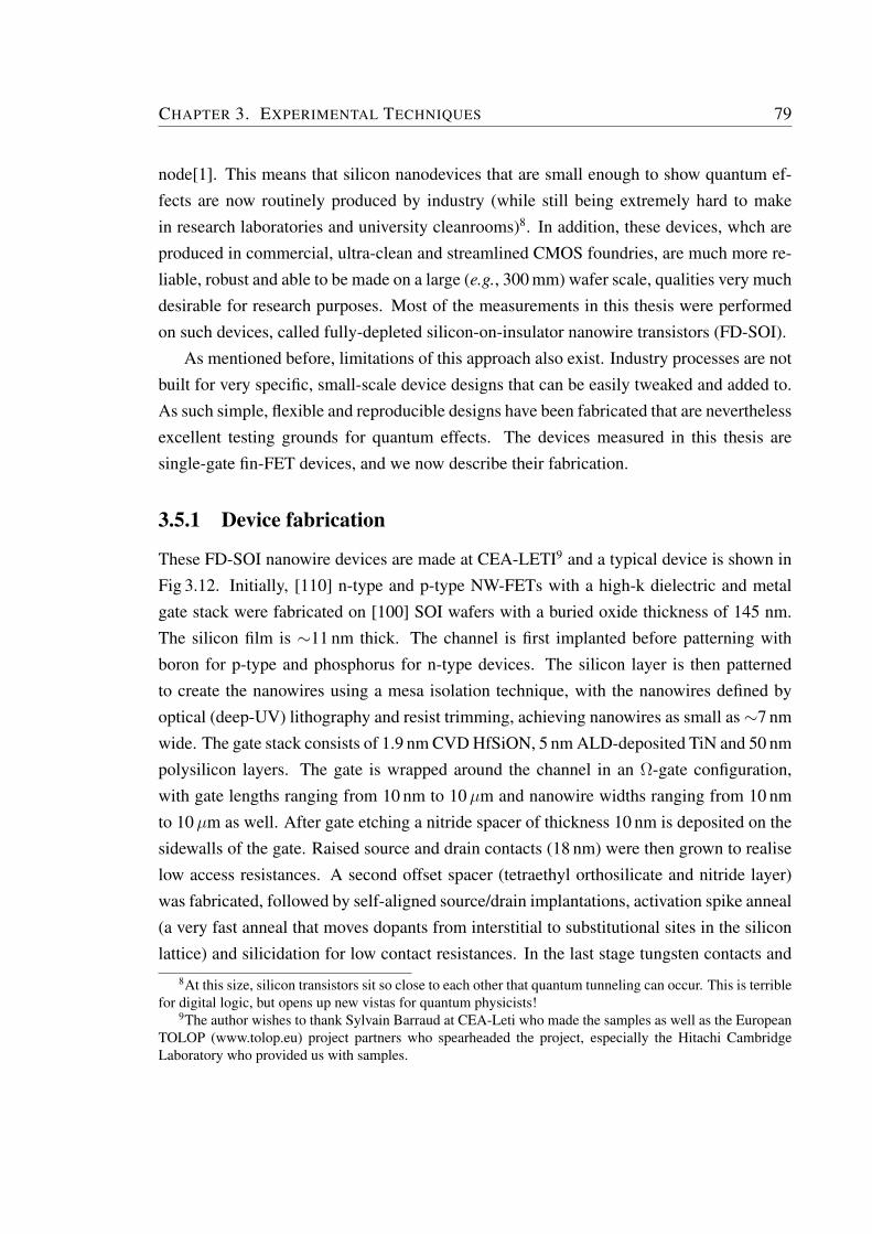
CHAPTER 3. EXPERIMENTAL TECHNIQUES 79
node[1]. This means that silicon nanodevices that are small enough to show quantum ef-fects are now routinely produced by industry (while still being extremely hard to makein research laboratories and university cleanrooms)8. In addition, these devices, whch areproduced in commercial, ultra-clean and streamlined CMOS foundries, are much more re-liable, robust and able to be made on a large (e.g., 300 mm) wafer scale, qualities very muchdesirable for research purposes. Most of the measurements in this thesis were performedon such devices, called fully-depleted silicon-on-insulator nanowire transistors (FD-SOI).
As mentioned before, limitations of this approach also exist. Industry processes are notbuilt for very specific, small-scale device designs that can be easily tweaked and added to.As such simple, flexible and reproducible designs have been fabricated that are neverthelessexcellent testing grounds for quantum effects. The devices measured in this thesis aresingle-gate fin-FET devices, and we now describe their fabrication.
3.5.1 Device fabrication
These FD-SOI nanowire devices are made at CEA-LETI9 and a typical device is shown inFig 3.12. Initially, [110] n-type and p-type NW-FETs with a high-k dielectric and metalgate stack were fabricated on [100] SOI wafers with a buried oxide thickness of 145 nm.The silicon film is ∼11 nm thick. The channel is first implanted before patterning withboron for p-type and phosphorus for n-type devices. The silicon layer is then patternedto create the nanowires using a mesa isolation technique, with the nanowires defined byoptical (deep-UV) lithography and resist trimming, achieving nanowires as small as∼7 nmwide. The gate stack consists of 1.9 nm CVD HfSiON, 5 nm ALD-deposited TiN and 50 nmpolysilicon layers. The gate is wrapped around the channel in an Ω-gate configuration,with gate lengths ranging from 10 nm to 10µm and nanowire widths ranging from 10 nmto 10µm as well. After gate etching a nitride spacer of thickness 10 nm is deposited on thesidewalls of the gate. Raised source and drain contacts (18 nm) were then grown to realiselow access resistances. A second offset spacer (tetraethyl orthosilicate and nitride layer)was fabricated, followed by self-aligned source/drain implantations, activation spike anneal(a very fast anneal that moves dopants from interstitial to substitutional sites in the siliconlattice) and silicidation for low contact resistances. In the last stage tungsten contacts and
8At this size, silicon transistors sit so close to each other that quantum tunneling can occur. This is terriblefor digital logic, but opens up new vistas for quantum physicists!
9The author wishes to thank Sylvain Barraud at CEA-Leti who made the samples as well as the EuropeanTOLOP (www.tolop.eu) project partners who spearheaded the project, especially the Hitachi CambridgeLaboratory who provided us with samples.
CHAPTER 3. EXPERIMENTAL TECHNIQUES 80
copper back-end process flows were used, finishing in 2µm oxide encapsulation. In somedevices, the channel is doped with phosphorus donors at a relatively low concentrationof 5×1017 cm−3, enabling us to study dopant physics in this subset of devices[104], asexplored in Chapter 6.
BOX5 nm
channel
gate (TiN)gate(poly-Si)
HfSiON
(c)
(a) (b)
(d)
TG
S
D
Figure 3.12: Foundry-fabricated FD-SOI devices from CEA-LETI. (a) 3D schematic ofwrap-around top gate device such as the ones measured in this thesis. (b) Simulationsperformed in Ref. [105] showing the formation of corner dots along the channel in thiskind of device. (c) TEM cross-section image from the previous reference of a typical deviceshowing channel gate and oxide layers. (d) Schematic form of (c), showing locations ofcorner dots simulated in (b), as well as showing possible donor location for a device with adoped channel.
3.5.2 Quantum dot formation
Because of the morphology of the wrap-around top gate, the electric field exerted by itis strongest at the topmost corners where the two gate faces meet. This has been calledthe ‘corner effect’ in fin-FET nanowires. This process has been studied in detail, withsimulations showing electron accumulation occurring first at the topmost corners[105]. Inaddition, as shown in Fig. 3.12, the presence of disorder creates confinement of the cornerchannels along the transport direction, leading to double dots in parallel. Localization isdriven by remote Coulomb charges at the SiO2/HfSiON interface and this attractive poten-tial leads to the formation of small quantum dots in the center of the channel edge, localisedaround 10 nm. This analysis is borne out by the large charging energies typically seen from
CHAPTER 3. EXPERIMENTAL TECHNIQUES 81
these dots[93][106][29], from the lever arm of the top gate being much higher than that ofthe back gate, and from the signatures of parallel double quantum dots seen in transportspectroscopy (no precise alignment of the quantum dot levels is seen, a feature required inseries transport). This corner effect and the resulting double quantum dot system has beenobserved by several research groups and is remarkably consistent, even across large wafers.
3.5.3 Measurement
Measurement of these devices is straightforward in some ways, thanks to their simplic-ity. The top gate, with a strong lever arm to both corner quantum dots, is connected toa tank circuit resonator for gate-based reflectometry of the kind described in Section 3.3.Due to the wrap-around Ω-gate geometry and extremely thin gate dieletric, the couplingof the dots to the gate and therefore to the resonator is extremely strong (lever arms are∼0.9), resulting in excellent results using dispersive readout through gate-based reflectom-etry as described in the previous section. In these devices, this technique has been shown toachieve sensitivities comparable to the best RF-SETs[93]. The other knob available to tunein the simplest single-gate devices is the back gate voltage; the back gate, or the siliconhandle wafer (scratched with a diamond scribe and attached to the measurement PCB witha conductive adhesive) is able to be used as a gate by flashing it with an LED to generatecharge carriers. In devices where the single wrap around gate is split into two gates facingeach other, the two gates can tune each dot independently and the back gate can then beused to tune the tunnel coupling.
In Chapters 4 and 6, we present measurements performed on these devices, to firstdevelop them into viable quantum dot devices and to then use them to couple quantum dotsto dopants.
Chapter 4
Gate-based charge sensing of a doublequantum dot in a silicon nanowire
In Chapter 1 of this thesis we stressed the importance of finding a material host and qubitarchitecture which will be a useful platform for a coupled dopant-dot system. In Chapter 2we discussed silicon as a material that presents multiple benefits for qubit coherence times,in addition to being a semiconductor suitable for both dopant and quantum dot qubits.Within the context of silicon, we would like to focus on a device architecture with the min-imum number of control gates possible for the quantum dot to assist with scaling up. Wetherefore explore a silicon-on-insulator nanowire finFET architecture with very small chan-nels, as well as localised channel doping, as described in Chapter 3. These devices havebeen shown to have corner states that can function as quantum dots[106], as well as havedopants in the channel[28, 107] through which transport has been measured[108]. Theyalso have the added benefit of being CMOS-foundry fabricated with excellent prospects forscalability.
In this Chapter, we seek to establish these devices as suitable for few-electron quantumdots, as well as work out theories of charge detection and quantum dot behaviour based onour chosen method of charge sensing, gate-based radiofrequency reflectometry (as intro-duced in Chapter 3). To that end, we present a few-electron double quantum dot establishedin a nanoscale CMOS silicon transistor. The chapter is divided into two parts. First, wedelve into gate-based reflectometry in these quantum dot systems, using it to explore a sin-gle quantum dot via its coupling to the lead (Fig. 4.1). Gate based charge sensing basedon RF-reflectometry is advantageous in terms of ultimate charge sensitivity[93] as well asfor reduction of circuit elements for quantum computation. We show that the coupling of
82
CHAPTER 4. GATE-BASED CHARGE SENSING OF A DOUBLE QUANTUM DOT IN A
SILICON NANOWIRE 83
the dot to the resonator can be used to develop tools valuable for cryogenic measurementand metrology of the qubit environment, such as primary thermometry and the sensing ofmicrowave amplitudes and pulse shapes.
In the second part, we move on to a double-quantum dot system in the silicon nanowiredevice and present Landau-Zener-Stuckelberg (LZS) measurements performed for a singleelectron charge qubit in silicon. In recent years LZS interferometry has gained prominenceas a viable method for all-electrical coherent control of few-electron quantum states. Firstdescribed for atomic states[109], it has been observed for superconducting quantum pointcontacts[110], interacting magnetic molecules[111], nitrogen vacancy centres in diamond[112] and ultracold molecular gases[113], among others. In the solid state, it has been usedto great effect for the control of semiconductor quantum dots[45, 50, 51, 114], in super-conducting qubits[115–117] and in donors in silicon[108]. However, nanodevices suitablefor LZS control can be geometrically complicated, with complex lithography requirementsmaking them hard to scale up. As such, it is of interest whether such coherent dynamicsof electronic charge states can be observed in standard commercial CMOS transistors. Inthis experiment, we apply microwaves to the double quantum dot system present in thedevice and use RF-reflectometry to observe a multi-regime LZS pattern, showing distinctsignatures of the single, double, and multiple-passage regimes of LZS interferometry in thesame device. We also observe a strong enhancement of the pattern at the points where theelectron tunnels out to the leads. The interference pattern is enhanced at these detectionpoints, and strongly suppressed when the microwave excitation is strong enough to drivethe electron across both of them, indicating that the state has been collapsed and a quan-tum superposition no longer exists. We study decoherence effects and present a theory ofLZS detected through the quantum capacitance signal of the double quantum dot, and putforward some applications of these multi-regime LZS measurements.
Before we delve into these experiments, we briefly discuss the sample and the measure-ment setup below. These measurements were carried out at the University of Cambridge,in conjunction with Dr. M. F. Gonzalez-Zalba, at the Hitachi Cambridge Laboratory.
Sample and setup
Our device is a silicon nanowire transistor, shown in (Fig. 4.2(a,b)), fabricated on asilicon-on-insulator substrate composed of a 145 nm buried oxide layer, a 11 nm thickintrinsic silicon layer, and an 850µm handle wafer which can be used as a global back
CHAPTER 4. GATE-BASED CHARGE SENSING OF A DOUBLE QUANTUM DOT IN A
SILICON NANOWIRE 84
gate. The silicon layer is etched to create a nanowire (200 nm long and 60 nm wide) bymeans of deep-UV lithography. A 40 nm wide wrap-around top gate is defined using aSiO2(0.8 nm)/HfSiON(1.9 nm) stack for the gate dielectric followed by TiN(5 nm)/poly-Si(50 nm) as the top gate material. The self-aligned source and drain (not representedon the sketch) are formed by ion implantation after the deposition of 20 nm thick Si3N4
spacers which prevent dopant diffusion into the channel.Measurements were performed at the base temperature of a Kelvinox K400 (“wet”) di-
lution refrigerator (40 mK), details of the measurement and wiring of which can be foundin Ref. [89]1. High sensitivity charge detection[93, 118] is achieved by radiofrequencyreflectometry on a tank circuit composed of a surface mounted inductance (390 nH), a par-asitic capacitance to ground Cp (∼1 pF) and the device capacitance between the transistortop gate and the channel. RF-reflectometry is performed close to the resonance frequency(313 MHz) and the reflected signal amplified by a low noise cryogenic amplifier. The sig-nal is further amplified and demodulated at room temperature as shown in Fig. 4.2(a). Anon-board bias tee is used to apply both DC and RF voltages on the top gate. Additionally,a fast line terminating at a 50 Ω-matched on-PCB stripline is used to deliver microwaves tothe sample. The undoped silicon substrate is activated by flashing a surface mounted blueLED to generate free carriers and can then be used as a back gate[119]. Applying a voltageto the top gate of the fully depleted device creates accumulation, which occurs first at thetopmost corners creating a double quantum dot in parallel[106, 107, 120].
4.1 Primary thermometry
Primary thermometry is the measurement of absolute temperature without the need for cal-ibration against an external thermometer. At millikelvin temperatures, Coulomb blockadethermometry (CBT)[92, 121] is popular because it can be readily performed using elec-tronic devices exhibiting transport. However, transport and its measurement are slow, andthere are regimes of interest (for example, a quantum dot coupled to only one of the leads) inwhich electronic transport is not established or possible. Other primary thermometry tech-niques exist, such as Josephson noise thermometry[122] and shot noise thermometry[123].However, the former requires a superconducting element, and noise thermometry in gen-
1Most details of this system are very similar in terms of filtering and anchoring, to the UCL cryogen-free“dry” dilution refrigerator described in Chapter 3. The low-noise-amplifier used here, a key component, isa Quinstar QCA-U350-30H anchored at the 4K plate, providing ∼40 dB amplification with a nominal 2.8 Knoise temperature at 350 MHz.
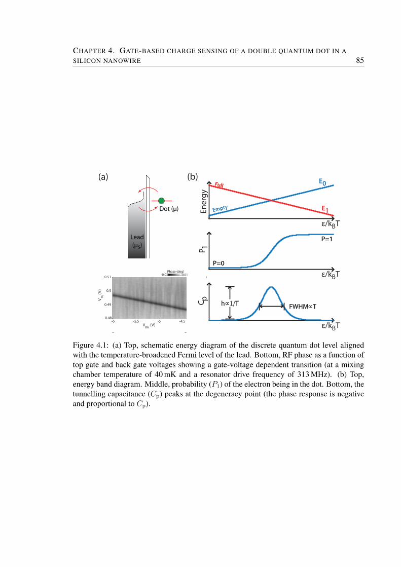
CHAPTER 4. GATE-BASED CHARGE SENSING OF A DOUBLE QUANTUM DOT IN A
SILICON NANOWIRE 85
Dot (μ)
Lead(μs)
VBG
(V)-6 -5.5 -5 -4.5
V TG(V
)
0.48
0.49
0.5
0.51-0.03 0.01
Phase (deg)
(a) E0
E1Ener
gyP 1
C p
(b)
FWHM∝Th∝1/T
P=0
P=1
ε/kBT
ε/kBT
ε/kBT
Full
Empty
Figure 4.1: (a) Top, schematic energy diagram of the discrete quantum dot level alignedwith the temperature-broadened Fermi level of the lead. Bottom, RF phase as a function oftop gate and back gate voltages showing a gate-voltage dependent transition (at a mixingchamber temperature of 40 mK and a resonator drive frequency of 313 MHz). (b) Top,energy band diagram. Middle, probability (P1) of the electron being in the dot. Bottom, thetunnelling capacitance (Cp) peaks at the degeneracy point (the phase response is negativeand proportional to Cp).
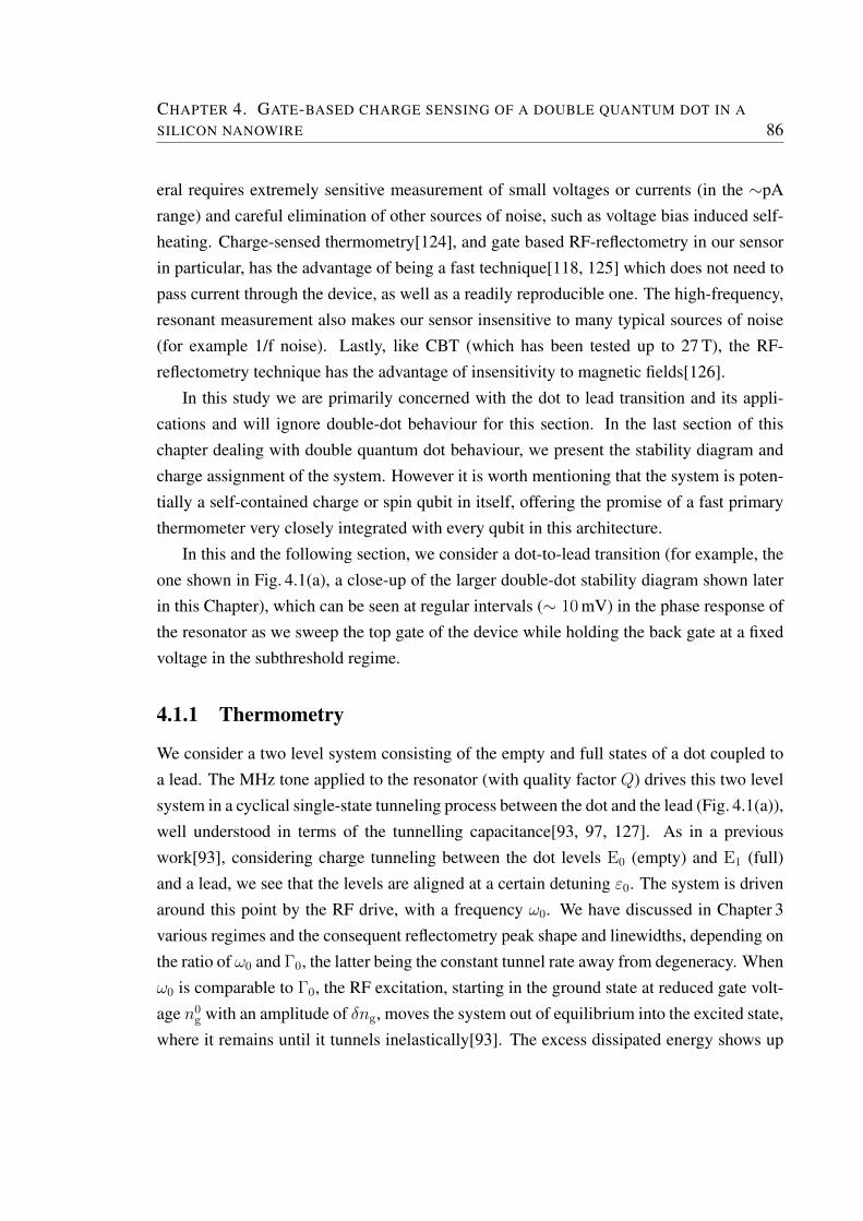
CHAPTER 4. GATE-BASED CHARGE SENSING OF A DOUBLE QUANTUM DOT IN A
SILICON NANOWIRE 86
eral requires extremely sensitive measurement of small voltages or currents (in the ∼pArange) and careful elimination of other sources of noise, such as voltage bias induced self-heating. Charge-sensed thermometry[124], and gate based RF-reflectometry in our sensorin particular, has the advantage of being a fast technique[118, 125] which does not need topass current through the device, as well as a readily reproducible one. The high-frequency,resonant measurement also makes our sensor insensitive to many typical sources of noise(for example 1/f noise). Lastly, like CBT (which has been tested up to 27 T), the RF-reflectometry technique has the advantage of insensitivity to magnetic fields[126].
In this study we are primarily concerned with the dot to lead transition and its appli-cations and will ignore double-dot behaviour for this section. In the last section of thischapter dealing with double quantum dot behaviour, we present the stability diagram andcharge assignment of the system. However it is worth mentioning that the system is poten-tially a self-contained charge or spin qubit in itself, offering the promise of a fast primarythermometer very closely integrated with every qubit in this architecture.
In this and the following section, we consider a dot-to-lead transition (for example, theone shown in Fig. 4.1(a), a close-up of the larger double-dot stability diagram shown laterin this Chapter), which can be seen at regular intervals (∼ 10 mV) in the phase response ofthe resonator as we sweep the top gate of the device while holding the back gate at a fixedvoltage in the subthreshold regime.
4.1.1 Thermometry
We consider a two level system consisting of the empty and full states of a dot coupled toa lead. The MHz tone applied to the resonator (with quality factor Q) drives this two levelsystem in a cyclical single-state tunneling process between the dot and the lead (Fig. 4.1(a)),well understood in terms of the tunnelling capacitance[93, 97, 127]. As in a previouswork[93], considering charge tunneling between the dot levels E0 (empty) and E1 (full)and a lead, we see that the levels are aligned at a certain detuning ε0. The system is drivenaround this point by the RF drive, with a frequency ω0. We have discussed in Chapter 3various regimes and the consequent reflectometry peak shape and linewidths, depending onthe ratio of ω0 and Γ0, the latter being the constant tunnel rate away from degeneracy. Whenω0 is comparable to Γ0, the RF excitation, starting in the ground state at reduced gate volt-age n0
g with an amplitude of δng, moves the system out of equilibrium into the excited state,where it remains until it tunnels inelastically[93]. The excess dissipated energy shows up
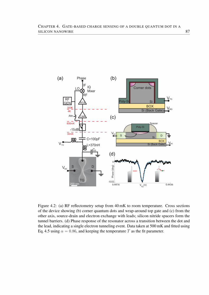
CHAPTER 4. GATE-BASED CHARGE SENSING OF A DOUBLE QUANTUM DOT IN A
SILICON NANOWIRE 87
VTG
(V)0.4416 0.4436
Phas
e (d
eg)
-0.02
0
L=370nHVTG
VSD
200 nm
C=100pF
LO
RF
IF
4K
RFGEN
Phase
30mK
Attn. LNA
800mK
RTA
300K
Cp
(a) (b)
(c)
(d)
SiBOX
Si (Back Gate)
VTG
VBG
Poly-Si
Corner dots
VSD
VBG
SiBOX
Si (Back Gate)
Poly-Si
S D
Spacer
-15 dB
TG
S D
IQ Mixer
Phase
Figure 4.2: (a) RF reflectometry setup from 40 mK to room temperature. Cross sectionsof the device showing (b) corner quantum dots and wrap-around top gate and (c) from theother axis, source-drain and electron exchange with leads; silicon nitride spacers form thetunnel barriers. (d) Phase response of the resonator across a transition between the dot andthe lead, indicating a single electron tunneling event. Data taken at 500 mK and fitted usingEq. 4.5 using α = 0.86, and keeping the temperature T as the fit parameter.
CHAPTER 4. GATE-BASED CHARGE SENSING OF A DOUBLE QUANTUM DOT IN A
SILICON NANOWIRE 88
as a change in the reflected power from the resonator, while a dispersive signal, manifestingas an additional tunneling capacitance Ct, is detected when electrons tunnel out of phasewith the RF cycle. However in the case where Γ0 ω0, that is, in the regime of a tunnelrate much higher than the RF driving frequency, the effective resistance entering into thecomplex admittance (Y = 1/∆R + iω0∆C) diverges[95]. Therefore, at high tunnel rates,no power is dissipated and electron tunneling is elastic. In this experiment our dot-to-leadtransitions are in this regime, and we will therefore consider this limit. (In the next section,we will show that the fact that we are in the double-passage regime of Landau-Zener inter-ferometry confirms this assumption, and that our tunnel rate is∼10 GHz, much higher thanour RF drive frequency at 300 MHz.)
The dynamics of the charge tunneling process can be described by a masterequation[97]:
P0 = Γ−P1 − Γ+P0, P1 = Γ+P0 − Γ−P1 (4.1)
which reduces to solving the differential equation
P1(t) + Γ0P1(t) = Γ+(t) (4.2)
due to probability conservation and the fact that Γ+ + Γ− = Γ0. Here Γ+ and Γ− are thetunneling rates into and out of the dot, while P0 is the probability of the electron beingoutside the dot and P1 is the probability of the electron being in the dot. Because of the rfdrive P1 shows up in the dispersive readout as the tunneling capacitance term:
Ct(t) = (eα)2 dP1
dε(4.3)
where α is the gate lever arm, defined as the conversion ratio of the applied gate voltageto the resulting shift in the dot energy levels. This generates a resonator phase shift ∆φ ∝Ct(t) and an average phase shift 〈∆φ〉. We can then arrive at an analytical expressionfor 〈∆φ〉 by expanding the tunnel rates in Eq. 4.2 around n0
g to the first order of δng (anapproximation valid for δng kBT/EC),
〈∆φ〉 ' −πQCp
(eα)2
2kBT
1
cosh2( ∆E2kBT
)
1
1 + ω20/Γ
20
(4.4)
The phase response of the resonator is related to the effective change in the capacitance ofthe system ∆C as ∆φ ≈ −πQ∆C/Cp. In our system we consider the high tunnel rate
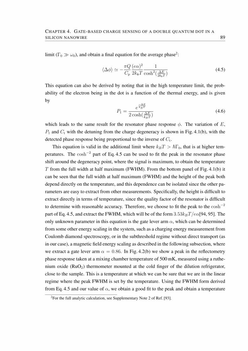
CHAPTER 4. GATE-BASED CHARGE SENSING OF A DOUBLE QUANTUM DOT IN A
SILICON NANOWIRE 89
limit (Γ0 ω0), and obtain a final equation for the average phase2:
〈∆φ〉 ' −πQCp
(eα)2
2kBT
1
cosh2( ∆E2kBT
)(4.5)
This equation can also be derived by noting that in the high temperature limit, the prob-ability of the electron being in the dot is a function of the thermal energy, and is givenby
P1 =e
−∆EkBT
2 cosh( ∆EkBT
)(4.6)
which leads to the same result for the resonator phase response φ. The variation of E,P1 and Ct with the detuning from the charge degeneracy is shown in Fig. 4.1(b), with thedetected phase response being proportional to the inverse of Ct.
This equation is valid in the additional limit where kBT > ~Γ0, that is at higher tem-peratures. The cosh−2 part of Eq. 4.5 can be used to fit the peak in the resonator phaseshift around the degeneracy point, where the signal is maximum, to obtain the temperatureT from the full width at half maximum (FWHM). From the bottom panel of Fig. 4.1(b) itcan be seen that the full width at half maximum (FWHM) and the height of the peak bothdepend directly on the temperature, and this dependence can be isolated since the other pa-rameters are easy to extract from other measurements. Specifically, the height is difficult toextract directly in terms of temperature, since the quality factor of the resonator is difficultto determine with reasonable accuracy. Therefore, we choose to fit the peak to the cosh−2
part of Eq. 4.5, and extract the FWHM, which will be of the form 3.53kBT/eα[94, 95]. Theonly unknown parameter in this equation is the gate lever arm α, which can be determinedfrom some other energy scaling in the system, such as a charging energy measurement fromCoulomb diamond spectroscopy, or in the subthreshold regime without direct transport (asin our case), a magnetic field energy scaling as described in the following subsection, wherewe extract a gate lever arm α = 0.86. In Fig. 4.2(b) we show a peak in the reflectometryphase response taken at a mixing chamber temperature of 500 mK, measured using a ruthe-nium oxide (RuO2) thermometer mounted at the cold finger of the dilution refrigerator,close to the sample. This is a temperature at which we can be sure that we are in the linearregime where the peak FWHM is set by the temperature. Using the FWHM form derivedfrom Eq. 4.5 and our value of α, we obtain a good fit to the peak and obtain a temperature
2For the full analytic calculation, see Supplementary Note 2 of Ref. [93].
CHAPTER 4. GATE-BASED CHARGE SENSING OF A DOUBLE QUANTUM DOT IN A
SILICON NANOWIRE 90
of ∼ 480 ± 66 mK. This is a primary value and does not need calibration against anotherthermometer. Some sources for the error in our measurement could be the insufficient pre-cision of the measurement of the energy scaling for the gate lever arm, the fact that theRuO2 thermometer at the coldfinger is some distance away from the device itself, as wellas the fact that at higher temperatures, the peak amplitude becomes smaller and the error onthe FWHM increases. In addition, at higher temperatures thermalization of the device cantake time, and the electron temperature can consequently vary from the temperature shownby the RuO2 thermometer.
We now discuss the lower limit set on the thermometer by the lifetime broadening dueto the coupling to the leads. As we decrease the temperature, we emerge out of the regimewhere kBT > ~Γ0 and into the regime where the peak is broadened by ~Γ0 and not by thetemperature. As discussed in Chapter 3 and above, in this regime the electron tunneling iselastic and has a purely capacitive response given by
Cp =(αe)2
π
~Γ0
(~Γ0)2 + (∆E)2(4.7)
Therefore, by fitting to the peak at a point where decreasing the temperature no longerhas any effect (in the case of a system with a high tunnel rate), we can extract the tunnelrate of the system. Indeed, at the lowest temperatures (40 mK, shown in Fig. 4.3(a)), weobtain a better fit to the peak using the Lorentzian form (Eq. 4.7) than to the temperature-broadened equation, which fits well for higher temperatures (400 mK and 1 K). From the fit,we obtain a tunnel rate of∼14.5 GHz, which matches well with the conclusions drawn fromour Landau-Zener experiment in the next section. We see that valuable information abouttunnel rates can be extracted from a gate-based reflectometry measurement, in addition toits use for primary thermometry.
In general the lower limit of the primary thermometer is given by the lifetime broaden-ing arising from the leads, and also by the fact that the tunnel rate needs to be larger thanthe resonator frequency, which is typically in the few hundred MHz range, to avoid excessdissipation. However, the study presented here is used to illustrate the different regimes inwhich the thermometry and tunnel rate detection can be performed. For a device similarto ours, but intended to be used for thermometry purposes, it would be possible to (a) en-gineer a dot with suitable tunnel rates to the leads using tunable tunnel barriers as well as(b) within the same device, find a different transition with a lower tunnel rate (the variabil-
CHAPTER 4. GATE-BASED CHARGE SENSING OF A DOUBLE QUANTUM DOT IN A
SILICON NANOWIRE 91
Temperature (K)0.2 0.4 0.6 0.8 1
FWH
M (m
eV)
0.1
0.25
Temperature (K)0.2 0.4 0.6 0.8 1
VTG (V)0.4418 0.4434
Phas
e (d
eg)
-0.05
-0.04
0
0.01
40mK400mK1K
(a)
(b) (c)
Figure 4.3: Peak shape, FWHM and amplitude with mixing chamber temperature. (a) Thephase response of the resonator at three different mixing chamber temperatures, measuredusing a RuO2 thermometer mounted at the coldfinger of the dilution fridge. The peak at40 mK is fitted using Eq. 4.7, while those at 400 mK and 1 K are fitted using Eq. 4.5. (b) and(c) show the extracted FWHM and the amplitudes of the peaks as we vary the temperature.In (b) a linear fit to the saturated FWHM values below 200 mK is used to extract the tunnelrate of the transition.
CHAPTER 4. GATE-BASED CHARGE SENSING OF A DOUBLE QUANTUM DOT IN A
SILICON NANOWIRE 92
ity of tunnel rates in the same device, within a large range from 100 MHz to 22 GHz, wasdemonstrated in Ref. [95] using different transitions of the same dot).
In Fig. 4.3(b) and (c) we present measurements showing the extracted FWHM andheight of the peak arising from the phase response of the resonator, with respect to mixingchamber temperature as detected by the external RuO2 resistance thermometer mountedclose to the sample. The trend shown is similar to CBT in quantum dots, where the FWHMof the peak decreases as the mixing chamber temperature is decreased. The trend in peakamplitude is similar. In our devices, as discussed, we use the saturation of the peak’sFWHM at low temperature to extract the tunnel rate of the transition, by fitting a line tofind the y-axis saturation point (y = c), which gives us the FWHM. From the FWHM andamplitude plots, in this case, we can only surmise therefore an electron temperature lowerthan ∼260 mK (obtained from the tunnel rate), since if it were higher than this value, thepeak width would saturate due to temperature (and not lifetime broadening).
RF drive and lever arms
One last crucial consideration for the kind of lineshape analysis and thermometry wepresent here is that in practice the device must be carefully set up so that the RF powersupplied to the sample is less than the thermal smearing due to kBT . We accomplish thisby lowering the RF amplitude and measuring the FWHM until it is no longer dependenton the RF amplitude, as shown in Fig. 4.4(a). In addition, to obtain numerical results fromthe peak fitting, the gate lever arm α must be obtained. This can be done by looking atan external energy scale of the system, for example the extent of Coulomb diamonds intransport; in our case, we monitor the dot-to-lead transition as we sweep the magnetic fieldand the shift in the peak towards higher or lower energy gives us a calibration of our gatelever arm in terms of energy, α = 0.86± 0.2, as shown in Fig. 4.4(b).
We now turn to a slightly different application of the gate-based reflectometry tech-nique, which is the calibration of microwave amplitudes.
4.2 Microwave sensing
Microwave pulses are yet another control mechanism vital to many qubit architectures[58,61]. However, due to the difficulties inherent in high-frequency microwave engineeringthere is often a trial-and-error process required to quantify pulse amplitudes and shapes
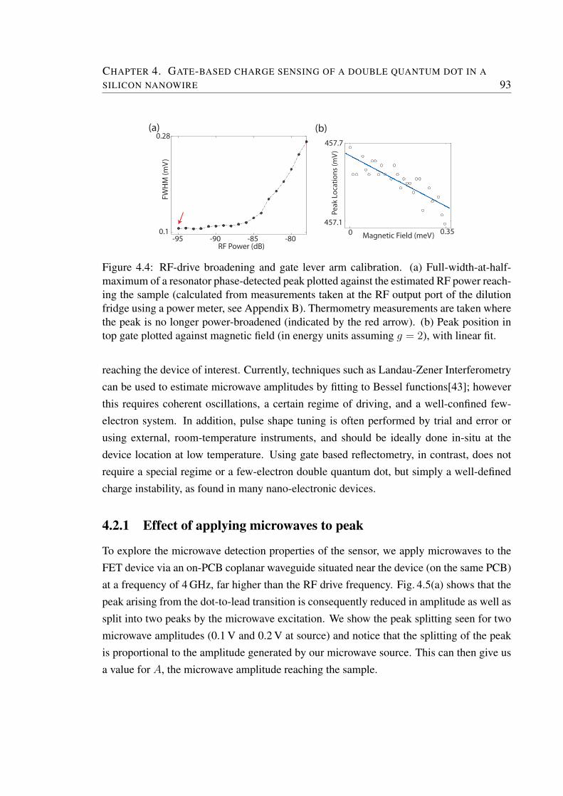
CHAPTER 4. GATE-BASED CHARGE SENSING OF A DOUBLE QUANTUM DOT IN A
SILICON NANOWIRE 93
RF Power (dB)-95 -90 -85 -80
FWH
M (m
V)
0.1
0.28(a) (b)
Magnetic Field (meV)0 0.35
Peak
Loc
atio
ns (m
V)
457.1
457.7
Figure 4.4: RF-drive broadening and gate lever arm calibration. (a) Full-width-at-half-maximum of a resonator phase-detected peak plotted against the estimated RF power reach-ing the sample (calculated from measurements taken at the RF output port of the dilutionfridge using a power meter, see Appendix B). Thermometry measurements are taken wherethe peak is no longer power-broadened (indicated by the red arrow). (b) Peak position intop gate plotted against magnetic field (in energy units assuming g = 2), with linear fit.
reaching the device of interest. Currently, techniques such as Landau-Zener Interferometrycan be used to estimate microwave amplitudes by fitting to Bessel functions[43]; howeverthis requires coherent oscillations, a certain regime of driving, and a well-confined few-electron system. In addition, pulse shape tuning is often performed by trial and error orusing external, room-temperature instruments, and should be ideally done in-situ at thedevice location at low temperature. Using gate based reflectometry, in contrast, does notrequire a special regime or a few-electron double quantum dot, but simply a well-definedcharge instability, as found in many nano-electronic devices.
4.2.1 Effect of applying microwaves to peak
To explore the microwave detection properties of the sensor, we apply microwaves to theFET device via an on-PCB coplanar waveguide situated near the device (on the same PCB)at a frequency of 4 GHz, far higher than the RF drive frequency. Fig. 4.5(a) shows that thepeak arising from the dot-to-lead transition is consequently reduced in amplitude as well assplit into two peaks by the microwave excitation. We show the peak splitting seen for twomicrowave amplitudes (0.1 V and 0.2 V at source) and notice that the splitting of the peakis proportional to the amplitude generated by our microwave source. This can then give usa value for A, the microwave amplitude reaching the sample.
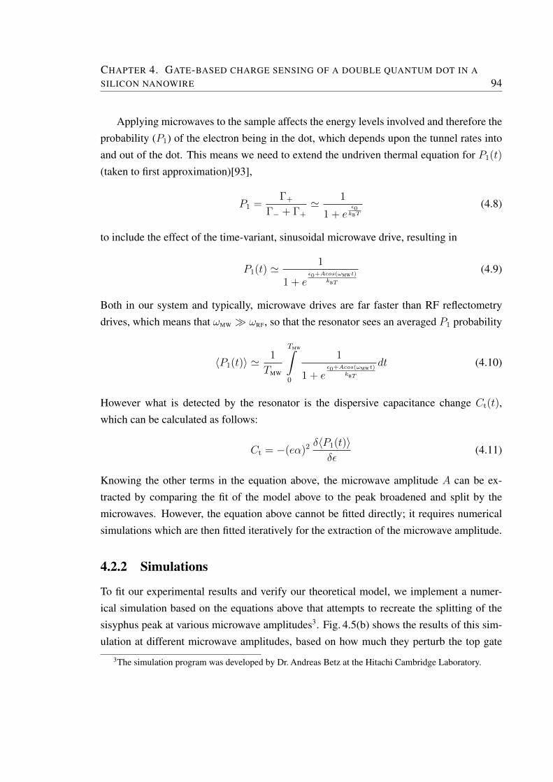
CHAPTER 4. GATE-BASED CHARGE SENSING OF A DOUBLE QUANTUM DOT IN A
SILICON NANOWIRE 94
Applying microwaves to the sample affects the energy levels involved and therefore theprobability (P1) of the electron being in the dot, which depends upon the tunnel rates intoand out of the dot. This means we need to extend the undriven thermal equation for P1(t)
(taken to first approximation)[93],
P1 =Γ+
Γ− + Γ+
' 1
1 + eε0kBT
(4.8)
to include the effect of the time-variant, sinusoidal microwave drive, resulting in
P1(t) ' 1
1 + eε0+Acos(ωMWt)
kBT
(4.9)
Both in our system and typically, microwave drives are far faster than RF reflectometrydrives, which means that ωMW ωRF, so that the resonator sees an averaged P1 probability
〈P1(t)〉 ' 1
TMW
TMW∫0
1
1 + eε0+Acos(ωMWt)
kBT
dt (4.10)
However what is detected by the resonator is the dispersive capacitance change Ct(t),which can be calculated as follows:
Ct = −(eα)2 δ〈P1(t)〉δε
(4.11)
Knowing the other terms in the equation above, the microwave amplitude A can be ex-tracted by comparing the fit of the model above to the peak broadened and split by themicrowaves. However, the equation above cannot be fitted directly; it requires numericalsimulations which are then fitted iteratively for the extraction of the microwave amplitude.
4.2.2 Simulations
To fit our experimental results and verify our theoretical model, we implement a numer-ical simulation based on the equations above that attempts to recreate the splitting of thesisyphus peak at various microwave amplitudes3. Fig. 4.5(b) shows the results of this sim-ulation at different microwave amplitudes, based on how much they perturb the top gate
3The simulation program was developed by Dr. Andreas Betz at the Hitachi Cambridge Laboratory.
CHAPTER 4. GATE-BASED CHARGE SENSING OF A DOUBLE QUANTUM DOT IN A
SILICON NANOWIRE 95
voltage4, parametrized as δng, for the bias point n0g = Cg/eVtg, with the charge degeneracy
occurring at n0g = 0.5. With δng = 0, the peak is not split at all, as expected, while with
δng = 0.01 and δng = 0.02 (with the latter splitting double that of the former as in the twoamplitudes shown in our measurements in Fig. 4.5(a)) we see the peak splits proportionallywith the increase in microwave amplitude. The model is in good qualitative agreementwith the experiment. The simulations are performed at a temperature of 200 mK and atunnel rate Γ0 = 15 GHz. At higher temperatures, the microwave and temperature effectsare decoupled, since the peak splitting remains the same, and can be fit separately, leadingto the microwave amplitude probe being useful at higher temperatures as well. Variationsin tunnel rates do not affect the splitting, but the overall signal intensity, as expected fromRefs. [93, 95]. The effects of temperature and tunnel rate vs microwave frequency can beseen in Appendix B.
Lastly, using our model in a situation where the applied excitation is in the form of apulse or a sawtooth ramp generates a very different response, as shown in Fig. 4.5(c) and(d), an effect which motivates further experimental work in this area. This can then be usedto calibrate other kinds of excitations; an effect especially important in the case of pulsing,for which the peak is sensitive to the pulse sharpness and the model can be used to engineerbest pulse frequencies and amplitudes for a given tunnel rate. In addition, the profile ofvery fast voltage pulses as seen by the qubit is extremely important for qubit manipulation.Applying such a pulse to the device and comparing it with the corresponding model couldallow direct comparisons and quantifications of pulse sharpness and amplitude.
In the next section we move on to the study of a double quantum dot system in thisdevice.
4.3 Multi-regime Landau-Zener Stuckelberg interferom-etry in a double quantum dot
In this section, we present a multi-level LZS interferometry study performed in a silicon-transistor-based charge qubit, which is tunnel coupled to a fermionic sea that allows us tocharacterise the qubit dynamics in the strong driving regime. We discussed LZS interfer-ometry in Chapter 2 and note that in the cases analysed in Ref. [43], the multiple passage
4These measurements are taken with the source and drain of the device grounded and there is a singlegate.
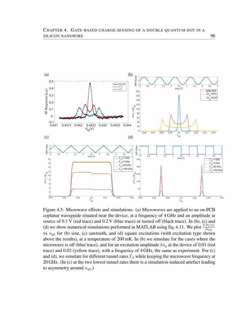
CHAPTER 4. GATE-BASED CHARGE SENSING OF A DOUBLE QUANTUM DOT IN A
SILICON NANOWIRE 96
Vtg (V)0.441 0.4415 0.442 0.4425 0.443 0.4435 0.444
RF R
espo
nse
(a.u
.)
-0.1
0
0.1
0.2
0.3
0.4
0.5MW OFF0.1 V0.2 V
(a) (b)
(c) (d)
Figure 4.5: Microwave effects and simulations. (a) Microwaves are applied to an on-PCBcoplanar waveguide situated near the device, at a frequency of 4 GHz and an amplitude atsource of 0.1 V (red trace) and 0.2 V (blue trace) or turned off (black trace). In (b), (c) and(d) we show numerical simulations performed in MATLAB using Eq. 4.11. We plot δ〈P1(t)〉
δng0
vs ng0 for (b) sine, (c) sawtooth, and (d) square excitations (with excitation type shownabove the results), at a temperature of 200 mK. In (b) we simulate for the cases where themicrowave is off (blue trace), and for an excitation amplitude δng at the device of 0.01 (redtrace) and 0.02 (yellow trace), with a frequency of 4 GHz, the same as experiment. For (c)and (d), we simulate for different tunnel rates Γ0 while keeping the microwave frequency at20 GHz. (In (c) at the two lowest tunnel rates there is a simulation-induced artefact leadingto asymmetry around ng0.)
CHAPTER 4. GATE-BASED CHARGE SENSING OF A DOUBLE QUANTUM DOT IN A
SILICON NANOWIRE 97
case is typically visible as an interference pattern as shown in Fig. 2.8(c). In Mach-Zehnderinterferometry in semiconductors, the double-passage problem has been separately studiedand applied as a method of qubit control[50]. However, in the present experiment, the sin-gle, double and multiple passage regimes are observable within the same device and at thesame drive frequency, and the microwave drive amplitude can be varied to switch betweenthe different regimes. Our measurement is performed by RF reflectometry directly on thegate (rather than using additional charge sensors); this can distinguish between electronstunnelling between the dots (a phase-conserving effect) and electrons tunnelling off the dotonto the leads (an effect involving relaxation and loss of phase information, analogous tothe photon detector in the optical interferometer), two processes which we briefly discussin the next section before presenting our results.
4.3.1 The quantum capacitance in a two-level system
For the specific two level system we consider here, the double quantum dot (DQD) witha single electron, there is a well-defined TLS with an avoided crossing at zero detuning(ε = 0), given an interdot tunnel coupling ∆. At large detuning, the electron is localised inthe left or right dot (we label these dot 1 and dot 2), while at low detuning it is delocalisedover the two dots, leading to hybridised ground and excited state energy levels, given byEq. 2.9. We are interested in the differential capacitance and changes in it, as seen from thetop gate, as that is where our resonator is coupled. This should provide us with a formulafor the detection of LZS interferometry via gate-based charge-sensing. Following Ref. [46],the differential capacitance can be defined as
Cdiff =d(Q1 +Q2)
dVG
(4.12)
where we take into account the sum of the charges Q1 and Q2 on the dots due to a certaingate voltage VG, and we know that
Q1 = CG1(VG − V1)
Q1 = −e〈n〉1 + (CS1 + CD1)V1 − CM(V2 − V1)(4.13)
and so on for the charge on the right dot Q2; with 〈n〉1 as the average charge number andV1 as the gate voltage on the left dot, with the dots coupled with mutual capacitance CM
and the left dot coupled to the source and drain by CS1 and CD1, respectively. Noting that
CHAPTER 4. GATE-BASED CHARGE SENSING OF A DOUBLE QUANTUM DOT IN A
SILICON NANOWIRE 98
〈n〉1 = −〈n〉2 when the dots exchange electrons, we can solve this set of linear equations(considering Q for both dots). We define the total capacitance of the dots CΣ1(2) and thelever arms α1(2) = CG1(2)/CΣ1(2). This gives us a differential capacitance
Cdiff = Cgeom + (eα)2d〈n〉dε
, (4.14)
where Cgeom ≈ α1(CS1 +CD1) + α2(CS2 +CD2) includes the static dot capacitance terms,and we define the lever arm for the double quantum dot as α− ≈ (α2−α1)/2. The averageelectron occupation (here for the right dot) can be expressed as a function of the groundand excited state probabilities Z = P−−P+, which is what we will need for our extensionof the Landau-Zener problem:
〈n〉 =1
2(1 +
ε
∆EZ) (4.15)
Noting that ∆E also depends on ε as E±(t) = ±12
√∆2 + ε(t)2 and combining Eqs. 4.14
and 4.15, we have our differential capacitance equation,
Cdiff = Cgeom + CQ(ε) + CT(ε)
CQ =(2eα−)2
2
(∆)2
(∆E)3Z
CT =(2eα−)2
2
ε
∆E
δZ
δε
(4.16)
where we have separated out the two contributions parametric on ε. The quantum capaci-tance CQ, arising from the curvature of the energy bands and the tunneling capacitance CT,arising from population redistribution processes such as relaxation (occurring on the sametimescale as the resonator, or faster) both need to be considered while analysing the effect ofthe qubit upon the resonator. In the theoretical analysis of our results we will use this frame-work for our four-state Landau-Zener experiment. This is essential both in understandingthe effect of the resonator (ideally negligible) on the interferometer, as well as in fitting theparameters of our system to extract useful information from the experiment[115, 116]. Wenow move on to our experimental results.
CHAPTER 4. GATE-BASED CHARGE SENSING OF A DOUBLE QUANTUM DOT IN A
SILICON NANOWIRE 99
4.3.2 DC transport measurements
This LZS study is performed in the same device presented in the previous sections, mea-sured with the same setup, as shown in Fig. 4.2(a). However we are now interested in thedouble quantum dot system instead of a single quantum dot to lead transition. We start byplotting the source-drain DC current ISD of the device in Fig. 4.6(a), as a function of thetop gate voltage, VTG, and the back-gate voltage, VBG. These measurements are taken at35 mK with a source drain bias voltage, VSD = 1 mV. At VTG ≈ 0.4− 0.6 we observe thetransistor turning on. The threshold top gate voltage depends upon the back gate voltageapplied and in general for a higher VBG, turn-on occurs at a lower top gate voltage. Nearthe threshold, we observe oscillatory features in the current indicating Coulomb blockade.This is due to the corner effect explored in Chapter 3 in these finFET devices, that confineselectrons onto quantum dots at the topmost corners of the transistor. The dots are wellcoupled to the source and drain allowing direct transport measurements to be taken in theseDC measurements. However, the white square, in Fig. 4.6(a), shows the region were thegate based rf-reflectometry measurements we present are taken. Here no direct transportthrough the transistor can occur as we are biased well below threshold and as the dots areweakly coupled to the source and drain reservoirs.5 The difference in the transport and re-flectometry regimes in their sensitivities shows that gate-based reflectometry is a valuabletool for charge-sensing where direct transport is not possible.
4.3.3 Stability diagram and dispersive detection
In Fig. 4.6(b), we see the demodulated phase response of the resonator as a function of thetop gate and back gate voltages. The phase response is sensitive to capacitance changesin the system. In the subthreshold regime of the transistor, where direct transport mea-surements are not sensitive enough, we observe the characteristic stability diagram of twocoupled quantum dots, as a function of the top gate and back gate voltages. As is typicalin these corner quantum dots which are located at the top corners of the wrap-around topgate[105], the charge transitions are coupled more strongly to the top gate than to the backgate.
RF reflectometry can be used to detect both dissipative and dispersive changes in thesystem under study. Dissipative processes such as a charge tunneling between a lead and a
5In addition, this means that both dots are well centered in the channel and are unlikely to be dopantsdiffused from the source and drain reservoir.
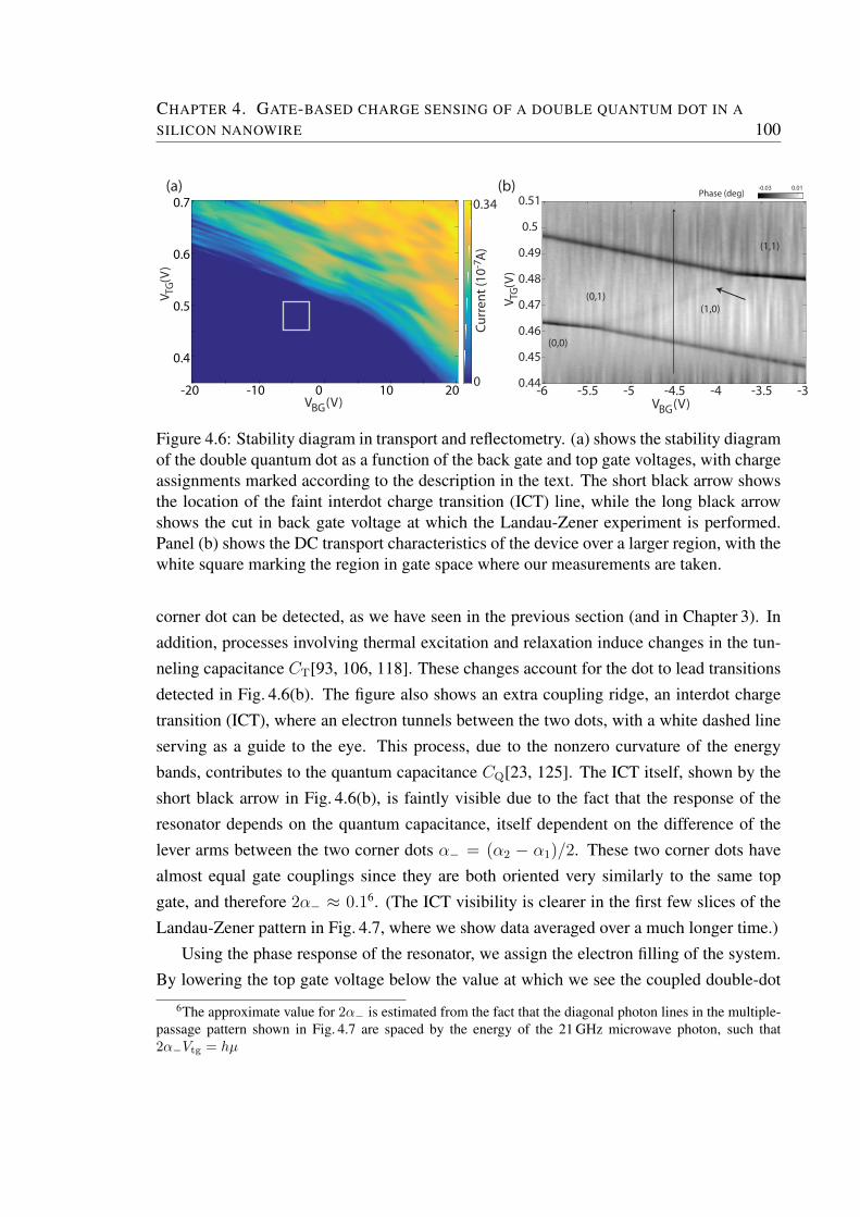
CHAPTER 4. GATE-BASED CHARGE SENSING OF A DOUBLE QUANTUM DOT IN A
SILICON NANOWIRE 100
-20 -10 0 10 20
0.4
0.5
0.6
0.7
Curr
ent (
10-7 A
)
0
0.34(a) (b)
VBG (V)-6 -5.5 -5 -4.5 -4 -3.5 -3
V TG(V
)
0.44
0.45
0.46
0.47
0.48
0.49
0.5
0.51-0.03 0.01
V TG(V
)
VBG (V)
Phase (deg)
(0,0)
(0,1)(1,0)
(1,1)
Figure 4.6: Stability diagram in transport and reflectometry. (a) shows the stability diagramof the double quantum dot as a function of the back gate and top gate voltages, with chargeassignments marked according to the description in the text. The short black arrow showsthe location of the faint interdot charge transition (ICT) line, while the long black arrowshows the cut in back gate voltage at which the Landau-Zener experiment is performed.Panel (b) shows the DC transport characteristics of the device over a larger region, with thewhite square marking the region in gate space where our measurements are taken.
corner dot can be detected, as we have seen in the previous section (and in Chapter 3). Inaddition, processes involving thermal excitation and relaxation induce changes in the tun-neling capacitance CT[93, 106, 118]. These changes account for the dot to lead transitionsdetected in Fig. 4.6(b). The figure also shows an extra coupling ridge, an interdot chargetransition (ICT), where an electron tunnels between the two dots, with a white dashed lineserving as a guide to the eye. This process, due to the nonzero curvature of the energybands, contributes to the quantum capacitance CQ[23, 125]. The ICT itself, shown by theshort black arrow in Fig. 4.6(b), is faintly visible due to the fact that the response of theresonator depends on the quantum capacitance, itself dependent on the difference of thelever arms between the two corner dots α− = (α2 − α1)/2. These two corner dots havealmost equal gate couplings since they are both oriented very similarly to the same topgate, and therefore 2α− ≈ 0.16. (The ICT visibility is clearer in the first few slices of theLandau-Zener pattern in Fig. 4.7, where we show data averaged over a much longer time.)
Using the phase response of the resonator, we assign the electron filling of the system.By lowering the top gate voltage below the value at which we see the coupled double-dot
6The approximate value for 2α− is estimated from the fact that the diagonal photon lines in the multiple-passage pattern shown in Fig. 4.7 are spaced by the energy of the 21 GHz microwave photon, such that2α−Vtg = hµ
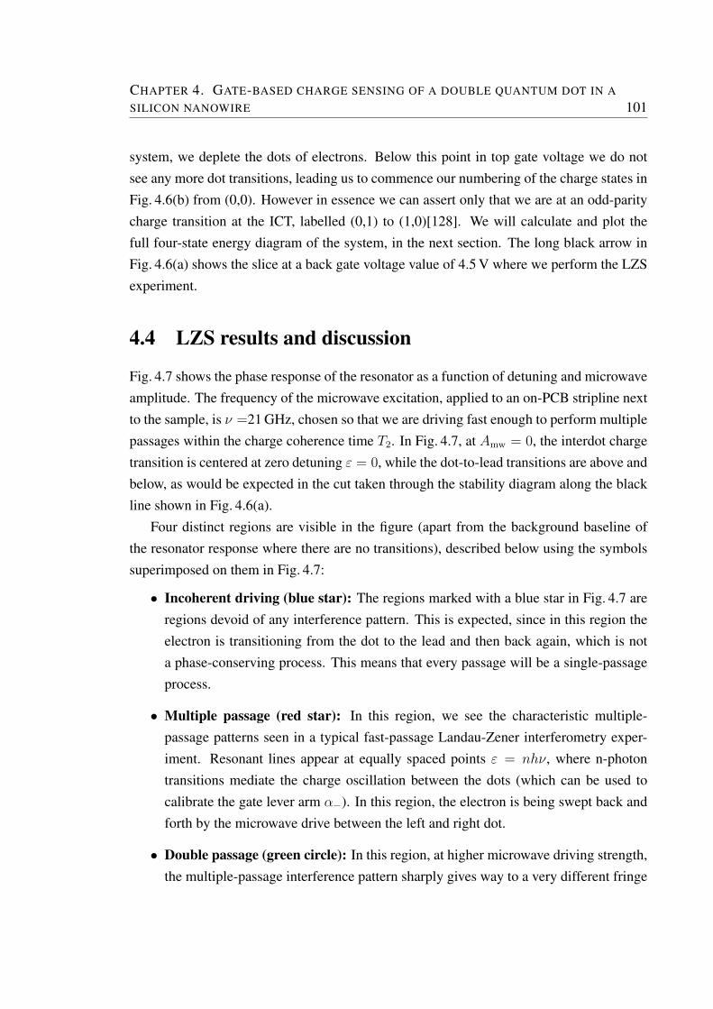
CHAPTER 4. GATE-BASED CHARGE SENSING OF A DOUBLE QUANTUM DOT IN A
SILICON NANOWIRE 101
system, we deplete the dots of electrons. Below this point in top gate voltage we do notsee any more dot transitions, leading us to commence our numbering of the charge states inFig. 4.6(b) from (0,0). However in essence we can assert only that we are at an odd-paritycharge transition at the ICT, labelled (0,1) to (1,0)[128]. We will calculate and plot thefull four-state energy diagram of the system, in the next section. The long black arrow inFig. 4.6(a) shows the slice at a back gate voltage value of 4.5 V where we perform the LZSexperiment.
4.4 LZS results and discussion
Fig. 4.7 shows the phase response of the resonator as a function of detuning and microwaveamplitude. The frequency of the microwave excitation, applied to an on-PCB stripline nextto the sample, is ν =21 GHz, chosen so that we are driving fast enough to perform multiplepassages within the charge coherence time T2. In Fig. 4.7, at Amw = 0, the interdot chargetransition is centered at zero detuning ε = 0, while the dot-to-lead transitions are above andbelow, as would be expected in the cut taken through the stability diagram along the blackline shown in Fig. 4.6(a).
Four distinct regions are visible in the figure (apart from the background baseline ofthe resonator response where there are no transitions), described below using the symbolssuperimposed on them in Fig. 4.7:
• Incoherent driving (blue star): The regions marked with a blue star in Fig. 4.7 areregions devoid of any interference pattern. This is expected, since in this region theelectron is transitioning from the dot to the lead and then back again, which is nota phase-conserving process. This means that every passage will be a single-passageprocess.
• Multiple passage (red star): In this region, we see the characteristic multiple-passage patterns seen in a typical fast-passage Landau-Zener interferometry exper-iment. Resonant lines appear at equally spaced points ε = nhν, where n-photontransitions mediate the charge oscillation between the dots (which can be used tocalibrate the gate lever arm α−). In this region, the electron is being swept back andforth by the microwave drive between the left and right dot.
• Double passage (green circle): In this region, at higher microwave driving strength,the multiple-passage interference pattern sharply gives way to a very different fringe
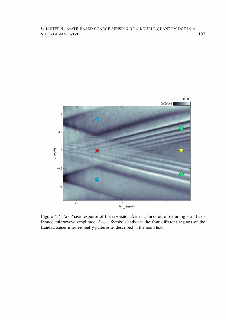
CHAPTER 4. GATE-BASED CHARGE SENSING OF A DOUBLE QUANTUM DOT IN A
SILICON NANOWIRE 102
Figure 4.7: (a) Phase response of the resonator ∆φ as a function of detuning ε and cal-ibrated microwave amplitude Amw. Symbols indicate the four different regions of theLandau-Zener interferometry patterns as described in the main text.
CHAPTER 4. GATE-BASED CHARGE SENSING OF A DOUBLE QUANTUM DOT IN A
SILICON NANOWIRE 103
pattern, where the individual photon lines are no longer visible. In addition, we notethat the visibility of the fringes is strongly enhanced, and we discuss the reasons forthis enhancement in the next section.
• Destruction of Interference (yellow triangle): Lastly, we increase the microwavedrive even higher and consider the resulting region, marked by a yellow triangle inFig. 4.7. Here there is an abrupt loss of the coherent interference pattern. It is alsothe point where the broadened dot-to-lead transitions overlap.
Before discussing these results in our theoretical framework, we look at the dependenceof this multi-regime pattern on the microwave drive frequency and use it to make a first-order estimate of the coherence time of the charge qubit, which we will need for the fit.
4.4.1 Frequency dependence
Our theoretical description considers our gate-based reflectometry setup in the semi-classical limit of a quantum system coupled to a classical resonator, with hν kBT ,an approach successful for the description of atom-light interactions. For us this requiresthat characteristic qubit times are much shorter than the period of the resonator, or thatν−1 h/∆, T1, T2. Since the resonator is much slower than the qubit, it sees the sta-tionary value for the occupation probabilities[46]. Our resonator frequency is 313 MHz,with a corresponding period of ∼3 ns. The full width at half maximum of the quantumcapacitance signal lineshape at the ICT gives us a rough measure of the tunnel couplingof the system, which is ∆ ∼33µeV or 8 GHz, while from our tunnel rate measurementsin the previous section, we know that the tunnel rate of the dot to the lead is very fast,∼15 GHz (which is why we are in the double passage regime upon encountering them),and that the “coupling” at these crossings is essentially, zero.
Results
In Section 2.4 we saw that the microwave frequency used to drive the Landau-Zener ex-periment can have a significant effect on the interference pattern, depending on the qubittimescales. Reducing the manipulation time below the coherence time of the system affectsthe central multiple-passage pattern first, since at some frequency we shift to an interme-diate regime of double-passage where the microwave period approaches T2. Subsequently,
CHAPTER 4. GATE-BASED CHARGE SENSING OF A DOUBLE QUANTUM DOT IN A
SILICON NANOWIRE 104
with a further lowering of the microwave frequency, we will go into the incoherent single-passage regime, where the electron phase coherence is lost within every passage, such thatmultiple passages are but an aggregation of single-passages. The electron phase coher-ence time in our strongly-driven TLS can therefore be studied by performing a microwavefrequency dependence of the LZS interferometry pattern (since of course we do not havedirect control over the T2 of the charge qubit). Fig. 4.8 shows the LZS interferometry studyperformed using three different microwave frequencies (29 GHz, 11 GHz, and 4.72 GHz,),where the change in driving frequency leads to differences in the maxima and minima po-sitions since the resonant lines appear at equally spaced points ε = nhν. We observe threeregimes: the quantum coherent regime in (a), the intermediate driving regime in (b) and theincoherent driving regime in (c). In (a), measured at 29 GHz, successive transitions throughthe avoided crossing are correlated, and clear interference fringes are visible. This indicatesthat ν−1 < T2. In (b) we observe fewer clear minima and maxima regions while others areblurred, indicating that ν−1 is approaching T2 and that we are close to the double-passageregime. In (c), Landau-Zener transitions are uncorrelated and we observe no interferencepattern, indicating ν−1 > T2. We see that in the enhanced regions, the double-passageinterference pattern persists up to 4.72GHz, or ∼200 ps, and we take this value of T2 as afirst guess for the fit to theory. We use T1 as a fitting parameter.
As we describe below, we find the best fit of theory to experiment with T1 and T2
in the same range, of a few hundred picoseconds, as is common for charge qubits in thesearchitectures[29, 46, 108]. In Chapter 6 we will use a different method to find the T1 and T2
of a similar charge qubit. These results indicate that our assumption that all characteristicqubit times are much shorter than the resonator period is accurate.
To develop an explanation for the different regions in our multi-regime LZS experiment,we need to gain a sense of the different energy levels of the system that come into play.For this purpose we now calculate the energy level diagram of this regime of the doublequantum dot.
4.4.2 Energy levels of the double quantum dot
We discussed the energy of a double quantum dot system calculated in the constant inter-action model in Section 2.2.2, for a single gate, as well as the reduced gate voltage ng. Inthe current device, we have a double quantum dot coupled to two gates, which can be rep-resented with a circuit diagram as shown in Fig. 4.9(a). The two gates are the top gate and
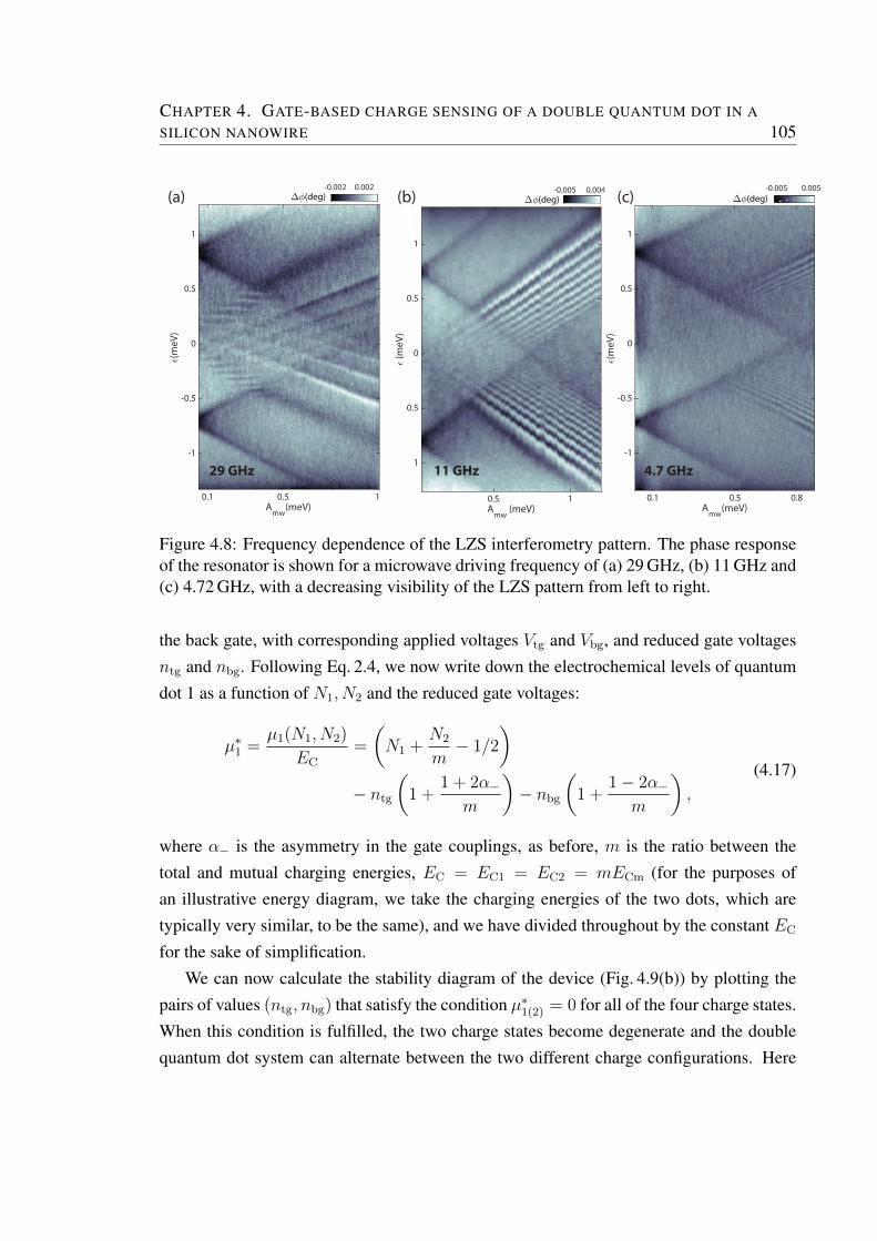
CHAPTER 4. GATE-BASED CHARGE SENSING OF A DOUBLE QUANTUM DOT IN A
SILICON NANOWIRE 105
29 GHz 11 GHz 4.7 GHz
(a) (b) (c)
Figure 4.8: Frequency dependence of the LZS interferometry pattern. The phase responseof the resonator is shown for a microwave driving frequency of (a) 29 GHz, (b) 11 GHz and(c) 4.72 GHz, with a decreasing visibility of the LZS pattern from left to right.
the back gate, with corresponding applied voltages Vtg and Vbg, and reduced gate voltagesntg and nbg. Following Eq. 2.4, we now write down the electrochemical levels of quantumdot 1 as a function of N1, N2 and the reduced gate voltages:
µ∗1 =µ1(N1, N2)
EC
=
(N1 +
N2
m− 1/2
)− ntg
(1 +
1 + 2α−m
)− nbg
(1 +
1− 2α−m
),
(4.17)
where α− is the asymmetry in the gate couplings, as before, m is the ratio between thetotal and mutual charging energies, EC = EC1 = EC2 = mECm (for the purposes ofan illustrative energy diagram, we take the charging energies of the two dots, which aretypically very similar, to be the same), and we have divided throughout by the constant EC
for the sake of simplification.We can now calculate the stability diagram of the device (Fig. 4.9(b)) by plotting the
pairs of values (ntg, nbg) that satisfy the condition µ∗1(2) = 0 for all of the four charge states.When this condition is fulfilled, the two charge states become degenerate and the doublequantum dot system can alternate between the two different charge configurations. Here
CHAPTER 4. GATE-BASED CHARGE SENSING OF A DOUBLE QUANTUM DOT IN A
SILICON NANOWIRE 106
we have used m = 10, i.e., a ten times lower mutual charging energy as compared to theindividual charging energies, as a typical value for semiconductor double quantum dots.To obtain 2α− = 0.1, we use the gate voltage spacing of the Landau-Zener photon lines inFig. 4.7, which gives us an energy scaling as per the equation dVtg = 2α− ∗ hν, where ν isthe frequency of the applied microwaves[129]. The reduced back gate voltage value wherethe experiment is performed, at the middle of the ICT line, corresponds to the bias pointn0
bg = 0.25.The energy diagram of the DQD in terms of the reduced gate voltages can now be
calculated, essentially taking a cut across the top gate, along the n0bg = 0.25 line. We plot
the total energy of the DQD forN1, N2 = 0, 1. Fig. 4.9(c) shows a plot of the reduced DQDenergies as a function of reduced gate voltage ntg for m = 10 and a = 0.1 as before, usinga tunnel coupling ∆c = EC/150.
Fig. 4.9(c) shows the energy diagram with different charge regions as indicated in themeasured stability diagram (Fig. 4.6(b)). From the figure we see that the central multiple-passage LZS pattern occurs at an anticrossing that is detected via the quantum capacitance(as described in Fig. 2.5(b) and Section 4.3.1), as the electron is swept back and forth acrossthe anticrossing. At the enhanced regions the electron is driven far enough that it can reachone of the two lower crossings shown in Fig. 4.9(c), where the electron can tunnel out fromdot to lead and be replaced by another from the Fermi sea of the lead, so that it can onlyperform a double passage before tunneling out and being detected. When both tunnelingpoints are reached by the microwave drive strength, the electron tunnels out in each passageacross the anticrossing.
4.5 Theoretical description
To interpret our multi-regime interference pattern, we use the LZS and quantum ca-pacitance theory discussed in Section 2.4 and 4.3.1 (extended in conjunction withDr. S. N. Shevchenko from the Center for Emergent Matter Science, RIKEN, Japan, whoalso performed simulations of the results). However, we now have to apply it, at leastinitially, while including all four of the interacting energy levels shown in Fig. 4.9.
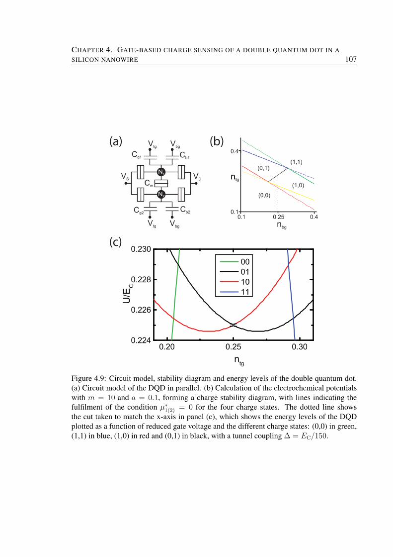
CHAPTER 4. GATE-BASED CHARGE SENSING OF A DOUBLE QUANTUM DOT IN A
SILICON NANOWIRE 107
nt
nbg
ntg
(0,0)
(0,1)
(1,0)
(1,1)
0.1 0.25 0.40.1
0.4
Cm
Cg1
VS
N1
N2
VD
VbgVtg
Cb1
Cg2
VbgVtg
Cb2
0.20 0.25 0.300.224
0.226
0.228
0.230
U/E
C
ntg
00011011
(a)
(c)
(b)
Figure 4.9: Circuit model, stability diagram and energy levels of the double quantum dot.(a) Circuit model of the DQD in parallel. (b) Calculation of the electrochemical potentialswith m = 10 and a = 0.1, forming a charge stability diagram, with lines indicating thefulfilment of the condition µ∗1(2) = 0 for the four charge states. The dotted line showsthe cut taken to match the x-axis in panel (c), which shows the energy levels of the DQDplotted as a function of reduced gate voltage and the different charge states: (0,0) in green,(1,1) in blue, (1,0) in red and (0,1) in black, with a tunnel coupling ∆ = EC/150.
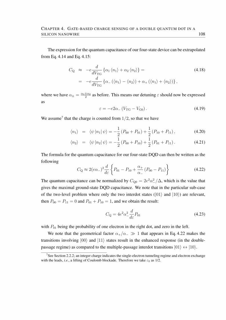
CHAPTER 4. GATE-BASED CHARGE SENSING OF A DOUBLE QUANTUM DOT IN A
SILICON NANOWIRE 108
The expression for the quantum capacitance of our four-state device can be extrapolatedfrom Eq. 4.14 and Eq. 4.15:
CQ ≈ −e d
dVTG
α1 〈n1〉+ α2 〈n2〉 = (4.18)
= −e d
dVTG
α− (〈n1〉 − 〈n2〉) + α+ (〈n1〉+ 〈n2〉) ,
where we have α± = α1±α2
2as before. This means our detuning ε should now be expressed
asε = −e2α− (VTG − VG0) . (4.19)
We assume7 that the charge is counted from 1/2, so that we have
〈n1〉 = 〈ψ |n1|ψ〉 = −1
2(P00 + P01) +
1
2(P10 + P11) , (4.20)
〈n2〉 = 〈ψ |n2|ψ〉 = −1
2(P00 + P10) +
1
2(P01 + P11) . (4.21)
The formula for the quantum capacitance for our four-state DQD can then be written as thefollowing
CQ ≈ 2(eα−)2 d
dε
P01 − P10 +
α+
α−(P00 − P11)
(4.22)
The quantum capacitance can be normalized by CQ0 = 2e2α2−/∆, which is the value that
gives the maximal ground-state DQD capacitance. We note that in the particular sub-caseof the two-level problem where only the two interdot states (|01〉 and |10〉) are relevant,then P00 = P11 = 0 and P01 + P10 = 1, and we obtain the result:
CQ = 4e2α2−d
dεP01 (4.23)
with P01 being the probability of one electron in the right dot, and zero in the left.We note that the geometrical factor α+/α− 1 that appears in Eq. 4.22 makes the
transitions involving |00〉 and |11〉 states result in the enhanced response (in the double-passage regime) as compared to the multiple-passage interdot transitions |01〉 ↔ |10〉.
7See Section 2.2.2; an integer charge indicates the single-electron tunneling regime and electron exchangewith the leads, i.e., a lifting of Coulomb blockade. Therefore we take ε0 as 1/2.
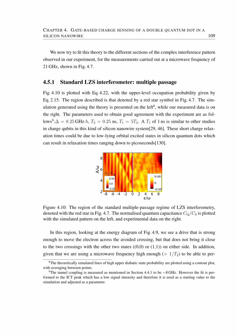
CHAPTER 4. GATE-BASED CHARGE SENSING OF A DOUBLE QUANTUM DOT IN A
SILICON NANOWIRE 109
We now try to fit this theory to the different sections of the complex interference patternobserved in our experiment, for the measurements carried out at a microwave frequency of21 GHz, shown in Fig. 4.7.
4.5.1 Standard LZS interferometer: multiple passage
Fig. 4.10 is plotted with Eq. 4.22, with the upper-level occupation probability given byEq. 2.15. The region described is that denoted by a red star symbol in Fig. 4.7. The sim-ulation generated using the theory is presented on the left8, while our measured data is onthe right. The parameters used to obtain good agreement with the experiment are as fol-lows9:∆ = 8.25 GHz·h, T2 = 0.25 ns, T1 = 5T2. A T1 of 1 ns is similar to other studiesin charge qubits in this kind of silicon nanowire system[29, 46]. These short charge relax-ation times could be due to low-lying orbital excited states in silicon quantum dots whichcan result in relaxation times ranging down to picoseconds[130].
A/ω
2
4
6
8
-8 -6 -4 -2 0 2 4 6 8ε/ω
Figure 4.10: The region of the standard multiple-passage regime of LZS interferometry,denoted with the red star in Fig. 4.7. The normalised quantum capacitanceCQ/C0 is plottedwith the simulated pattern on the left, and experimental data on the right.
In this region, looking at the energy diagram of Fig. 4.9, we see a drive that is strongenough to move the electron across the avoided crossing, but that does not bring it closeto the two crossings with the other two states ((0,0) or (1,1)) on either side. In addition,given that we are using a microwave frequency high enough (> 1/T2) to be able to per-
8The theoretically simulated lines of high upper diabatic state probability are plotted using a contour plot,with averaging between points.
9The tunnel coupling is measured as mentioned in Section 4.4.1 to be ∼8 GHz. However the fit is per-formed to the ICT peak which has a low signal intensity and therefore it is used as a starting value to thesimulation and adjusted as a parameter.
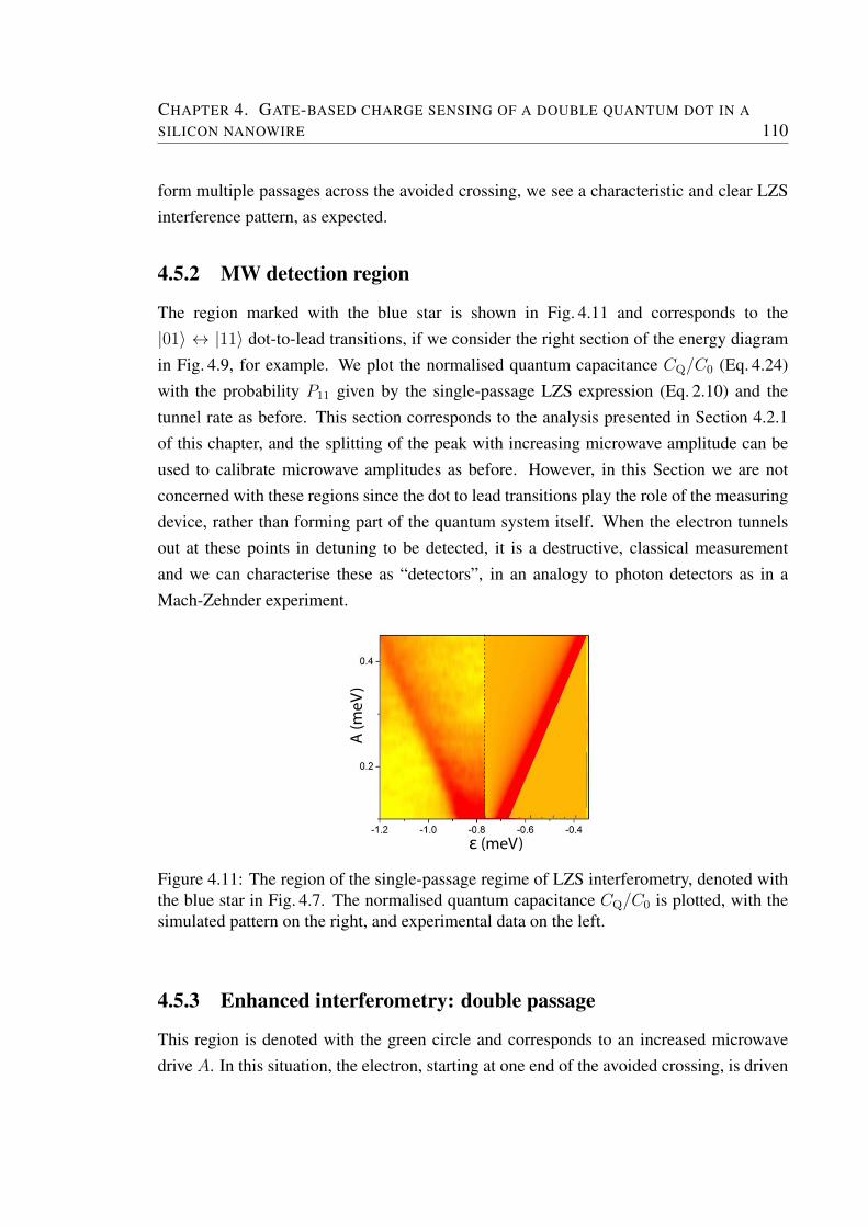
CHAPTER 4. GATE-BASED CHARGE SENSING OF A DOUBLE QUANTUM DOT IN A
SILICON NANOWIRE 110
form multiple passages across the avoided crossing, we see a characteristic and clear LZSinterference pattern, as expected.
4.5.2 MW detection region
The region marked with the blue star is shown in Fig. 4.11 and corresponds to the|01〉 ↔ |11〉 dot-to-lead transitions, if we consider the right section of the energy diagramin Fig. 4.9, for example. We plot the normalised quantum capacitance CQ/C0 (Eq. 4.24)with the probability P11 given by the single-passage LZS expression (Eq. 2.10) and thetunnel rate as before. This section corresponds to the analysis presented in Section 4.2.1of this chapter, and the splitting of the peak with increasing microwave amplitude can beused to calibrate microwave amplitudes as before. However, in this Section we are notconcerned with these regions since the dot to lead transitions play the role of the measuringdevice, rather than forming part of the quantum system itself. When the electron tunnelsout at these points in detuning to be detected, it is a destructive, classical measurementand we can characterise these as “detectors”, in an analogy to photon detectors as in aMach-Zehnder experiment.
A (m
eV)
ε (meV)
Figure 4.11: The region of the single-passage regime of LZS interferometry, denoted withthe blue star in Fig. 4.7. The normalised quantum capacitance CQ/C0 is plotted, with thesimulated pattern on the right, and experimental data on the left.
4.5.3 Enhanced interferometry: double passage
This region is denoted with the green circle and corresponds to an increased microwavedrive A. In this situation, the electron, starting at one end of the avoided crossing, is driven
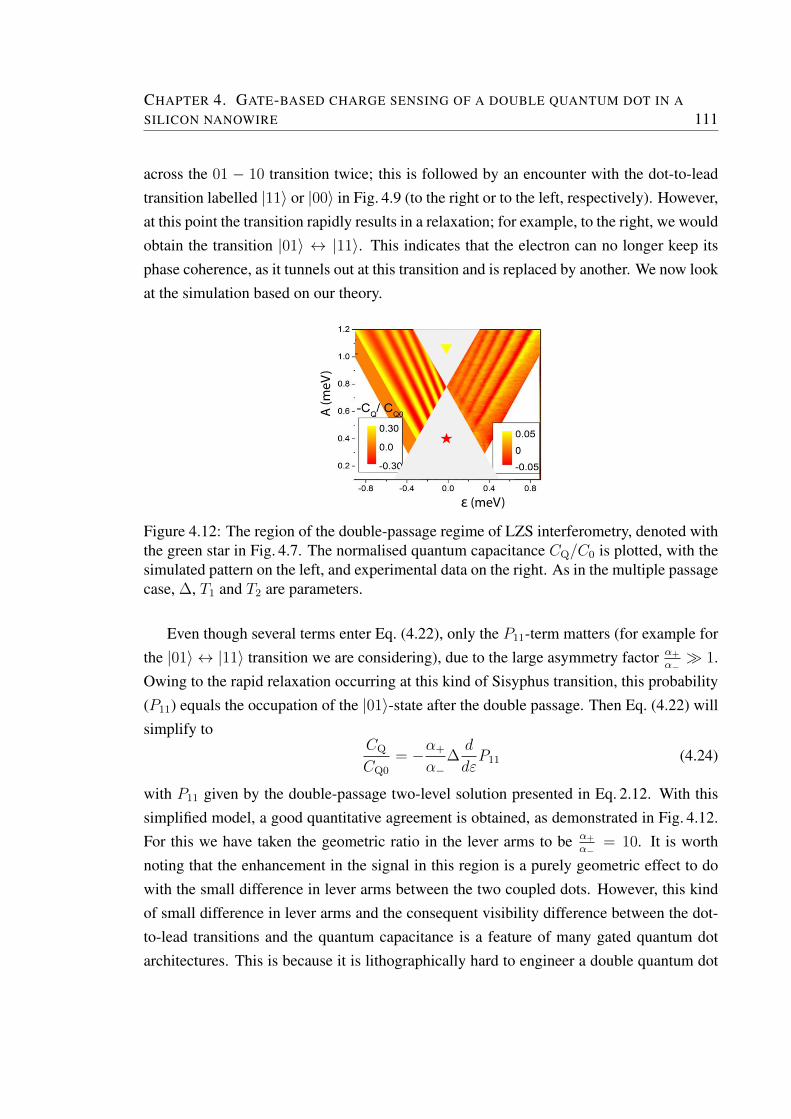
CHAPTER 4. GATE-BASED CHARGE SENSING OF A DOUBLE QUANTUM DOT IN A
SILICON NANOWIRE 111
across the 01 − 10 transition twice; this is followed by an encounter with the dot-to-leadtransition labelled |11〉 or |00〉 in Fig. 4.9 (to the right or to the left, respectively). However,at this point the transition rapidly results in a relaxation; for example, to the right, we wouldobtain the transition |01〉 ↔ |11〉. This indicates that the electron can no longer keep itsphase coherence, as it tunnels out at this transition and is replaced by another. We now lookat the simulation based on our theory.
A (m
eV)
ε (meV)
Figure 4.12: The region of the double-passage regime of LZS interferometry, denoted withthe green star in Fig. 4.7. The normalised quantum capacitance CQ/C0 is plotted, with thesimulated pattern on the left, and experimental data on the right. As in the multiple passagecase, ∆, T1 and T2 are parameters.
Even though several terms enter Eq. (4.22), only the P11-term matters (for example forthe |01〉 ↔ |11〉 transition we are considering), due to the large asymmetry factor α+
α− 1.
Owing to the rapid relaxation occurring at this kind of Sisyphus transition, this probability(P11) equals the occupation of the |01〉-state after the double passage. Then Eq. (4.22) willsimplify to
CQ
CQ0
= −α+
α−∆d
dεP11 (4.24)
with P11 given by the double-passage two-level solution presented in Eq. 2.12. With thissimplified model, a good quantitative agreement is obtained, as demonstrated in Fig. 4.12.For this we have taken the geometric ratio in the lever arms to be α+
α−= 10. It is worth
noting that the enhancement in the signal in this region is a purely geometric effect to dowith the small difference in lever arms between the two coupled dots. However, this kindof small difference in lever arms and the consequent visibility difference between the dot-to-lead transitions and the quantum capacitance is a feature of many gated quantum dotarchitectures. This is because it is lithographically hard to engineer a double quantum dot
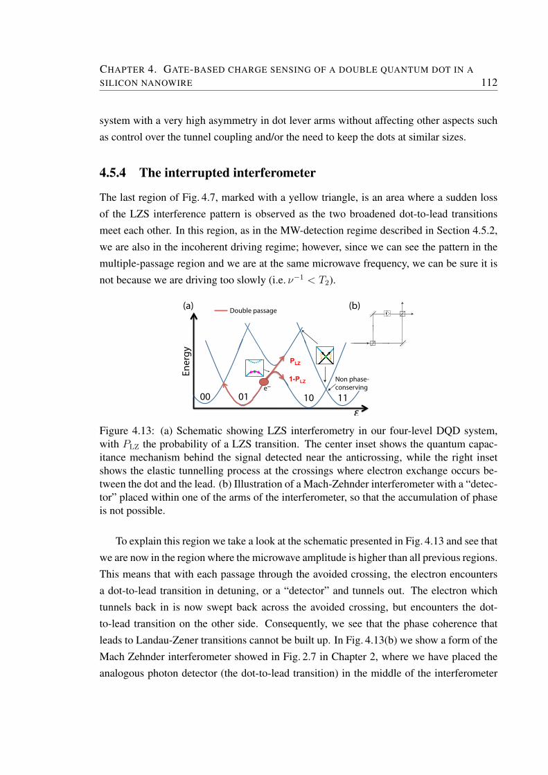
CHAPTER 4. GATE-BASED CHARGE SENSING OF A DOUBLE QUANTUM DOT IN A
SILICON NANOWIRE 112
system with a very high asymmetry in dot lever arms without affecting other aspects suchas control over the tunnel coupling and/or the need to keep the dots at similar sizes.
4.5.4 The interrupted interferometer
The last region of Fig. 4.7, marked with a yellow triangle, is an area where a sudden lossof the LZS interference pattern is observed as the two broadened dot-to-lead transitionsmeet each other. In this region, as in the MW-detection regime described in Section 4.5.2,we are also in the incoherent driving regime; however, since we can see the pattern in themultiple-passage region and we are at the same microwave frequency, we can be sure it isnot because we are driving too slowly (i.e. ν−1 < T2).
1-PLZ
PLZ
ε
Ener
gy
00 01 10 11
(a) (b)
Non phase-conserving
Double passage
e–
Figure 4.13: (a) Schematic showing LZS interferometry in our four-level DQD system,with PLZ the probability of a LZS transition. The center inset shows the quantum capac-itance mechanism behind the signal detected near the anticrossing, while the right insetshows the elastic tunnelling process at the crossings where electron exchange occurs be-tween the dot and the lead. (b) Illustration of a Mach-Zehnder interferometer with a “detec-tor” placed within one of the arms of the interferometer, so that the accumulation of phaseis not possible.
To explain this region we take a look at the schematic presented in Fig. 4.13 and see thatwe are now in the region where the microwave amplitude is higher than all previous regions.This means that with each passage through the avoided crossing, the electron encountersa dot-to-lead transition in detuning, or a “detector” and tunnels out. The electron whichtunnels back in is now swept back across the avoided crossing, but encounters the dot-to-lead transition on the other side. Consequently, we see that the phase coherence thatleads to Landau-Zener transitions cannot be built up. In Fig. 4.13(b) we show a form of theMach Zehnder interferometer showed in Fig. 2.7 in Chapter 2, where we have placed theanalogous photon detector (the dot-to-lead transition) in the middle of the interferometer
CHAPTER 4. GATE-BASED CHARGE SENSING OF A DOUBLE QUANTUM DOT IN A
SILICON NANOWIRE 113
path, after the beam splitter (the avoided crossing), to illustrate that the interferometry is,in a sense, “interrupted”.
4.6 Outlook and conclusion
In summary, in this chapter we have shown that gate based RF-reflectometry can be usedto perform fast, sensitive primary thermometry at millikelvin temperatures. We also showthat the tunneling capacitance peak responds quantifiably to microwave excitation and thatthis can potentially be used to calibrate the microwave amplitude arriving at the device. Wehave been able to develop a theoretical model and simulate qualitatively the effect of themicrowaves. Additionally, our sensor is implemented in a nanoscale CMOS silicon archi-tecture which is readily able to be mass-produced both for integration with conventionalelectronics as well as with current quantum computation schemes.
We have also reported dispersive readout of a double quantum dot in the channel of acommercial CMOS transistor. We read out the charge state of the system in a continuousnon-demolition regime by using the the dispersive response of a high-frequency resonator,discussed earlier in this chapter, which is coupled to the quantum system via the gate. Weuse microwaves to perform multiple fast passages through the qubits avoided crossing andwe observe the emergence of the LZS interferometry pattern, corresponding well to the-oretical predictions and previous experimental work. At stronger drives, however, usinga projective measurement to an even-parity charge state, we observe a strong geometricalenhancement of the readout signal. At even stronger drives, we perform a second projec-tive measurement which occurs during the coherent evolution, resulting in a loss of theinterference pattern. Using microwave pulses accessing different regimes of the LZS inter-ferometry, instead of a continuous drive this kind of novel multi-regime interference patterncould demonstrate a way to increase the state readout signal of coherent quantum systems,in addition to providing valuable insight into the field of single-electron analogues to opti-cal reflectometry. Potential fine control over the interferometry and the regimes is possible,by using fast pulses to drive back and forth across the avoided crossing, accumulate a fixedamount of phase by waiting, and then pulse just as far as the dot-to-lead crossing to read outthe phase with an enhanced signal. Lastly, our results demonstrate a way to integrate qubitcontrol, readout and the exploration of novel physical phenomena with existing large-scaleand robust CMOS technology.
CHAPTER 4. GATE-BASED CHARGE SENSING OF A DOUBLE QUANTUM DOT IN A
SILICON NANOWIRE 114
In the next chapters we will explore the idea of integrating dopants into this double-quantum dot architecture by performing a spin-dependent transport study on a dopant insilicon, and finally we will present a coupled hybrid dopant-dot system.
Chapter 5
Electrically Detected MagneticResonance of Selenium Donors in Silicon
5.1 Introduction: deep double donors in silicon
The previous chapter explored quantum dots in nanodevices in silicon, as well as ways toperform single-electron charge-sensing and qubit control in a scalable architecture. Ulti-mately, as stated before, we seek to combine this fast, readily tunable and versatile archi-tecture with a spin system that has been proven to have extremely long coherence times;donors in silicon. In this Chapter we employ the sensitive magnetic resonance technique ofEDMR (described in Chapter 3) to study a dopant in silicon that has potential for success-ful integration into nanodevices, in addition to coherence and relaxation times attractive forquantum computation.
As described in Chapter 1, the electron and nuclear spin of phosphorus donors in siliconhave been widely studied for qubit applications. These have been manipulated and read outvia their integration into electronic devices[6–8] as well as in the bulk[16, 131]. Arsenicand bismuth donors have also been studied in the bulk, but along with phosphorus, theseare all “shallow” dopants in silicon, that is, they are relatively close to the conduction bandand require little energy to ionise, as shown in Fig. 5.1.
The chalcogens in silicon, however, have not been studied in detail despite having mul-tiple characteristics making them viable as donor-based qubits, as well as useful systems forspintronics. The chalcogens are deep, “double” dopants in silicon; while group V dopants
115
CHAPTER 5. ELECTRICALLY DETECTED MAGNETIC RESONANCE OF SELENIUM
DONORS IN SILICON 116
like phosphorus have a single electron to donate, group VI dopants, such as selenium, havetwo bound electrons in the neutral state[132].
In this work we study one of this class of dopants, namely selenium, through the sensi-tive spin-to-charge conversion technique called Electrically Detected Magnetic Resonance(EDMR), first demonstrated in 1972 by Lepine[133]. EDMR has been the frontrunner ofdevice development and integration of dopant spins into single-atom spin qubit devicesin silicon, especially for phosphorus. Many aspects of the physics of donor spins, andtheir interactions with interface defects in silicon were understood through EDMR, as weremechanisms such as spin-dependent tunneling[84] and spin-to-charge conversion, whichare essential techniques in the readout of quantum dots[56][41] as well as for phospho-rus donor devices. In addition to applications for quantum information mentioned above,EDMR has been instrumental in the study of photovoltaics and disordered materials (suchas amorphous-Si:H, notably in the context of solar cells[134]).
Spin dependent transport in silicon is typically understood within the two frameworksof polarization-dependent models and spin-dependent recombination. Within these frame-works, there exist a variety of mechanisms, discussed in Section 5.1.3. However, in thecontext of donors in silicon, these mechanisms have been identified through experimentalstudies on the shallow donors only. It is conceivable that due to their double-donor na-ture and their strong binding energies, deep donors in silicon may give rise to previouslyunobserved EDMR mechanisms. Our study, performed on a bulk selenium-doped siliconsample using transport measurements, seeks to examine this hypothesis and we are inter-ested in identifying and isolating novel spin-to-charge conversion mechanisms in silicon.We also aim to gain understanding into a possible spin-to-charge conversion mechanismthat will lead us to the first chalcogen implanted devices. It is hoped that the study willshed light on spin-dependent transport processes involving a deep, double donor in silicon,which have not been observed before.
5.1.1 State of the art for chalcogens in silicon
The electronic structure of the chalcogens has been investigated[132, 135–140] for al-most thirty years now. Electronic structures and ionization energies were determined byDeep Level Transient Spectroscopy (DLTS)[135] and by Fourier Transform Infrared Spec-troscopy (FTIR) techniques on p-n diodes[132], while information on the excited statesof selenium was obtained through IR optical absorption spectroscopy both in natural[137]
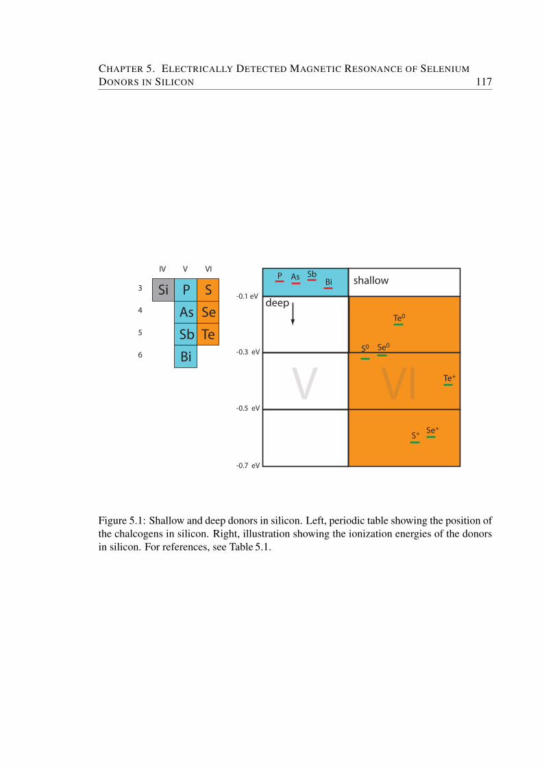
CHAPTER 5. ELECTRICALLY DETECTED MAGNETIC RESONANCE OF SELENIUM
DONORS IN SILICON 117
IV V VI
3
4
5
6
Si P S
As Se
Sb Te
Bi
P As SbBi
Te0
S0 Se0
Te+
Se+S+
-0.1 eV
-0.3 eV
-0.5 eV
-0.7 eV
VIV
shallow
deep
Figure 5.1: Shallow and deep donors in silicon. Left, periodic table showing the position ofthe chalcogens in silicon. Right, illustration showing the ionization energies of the donorsin silicon. For references, see Table 5.1.
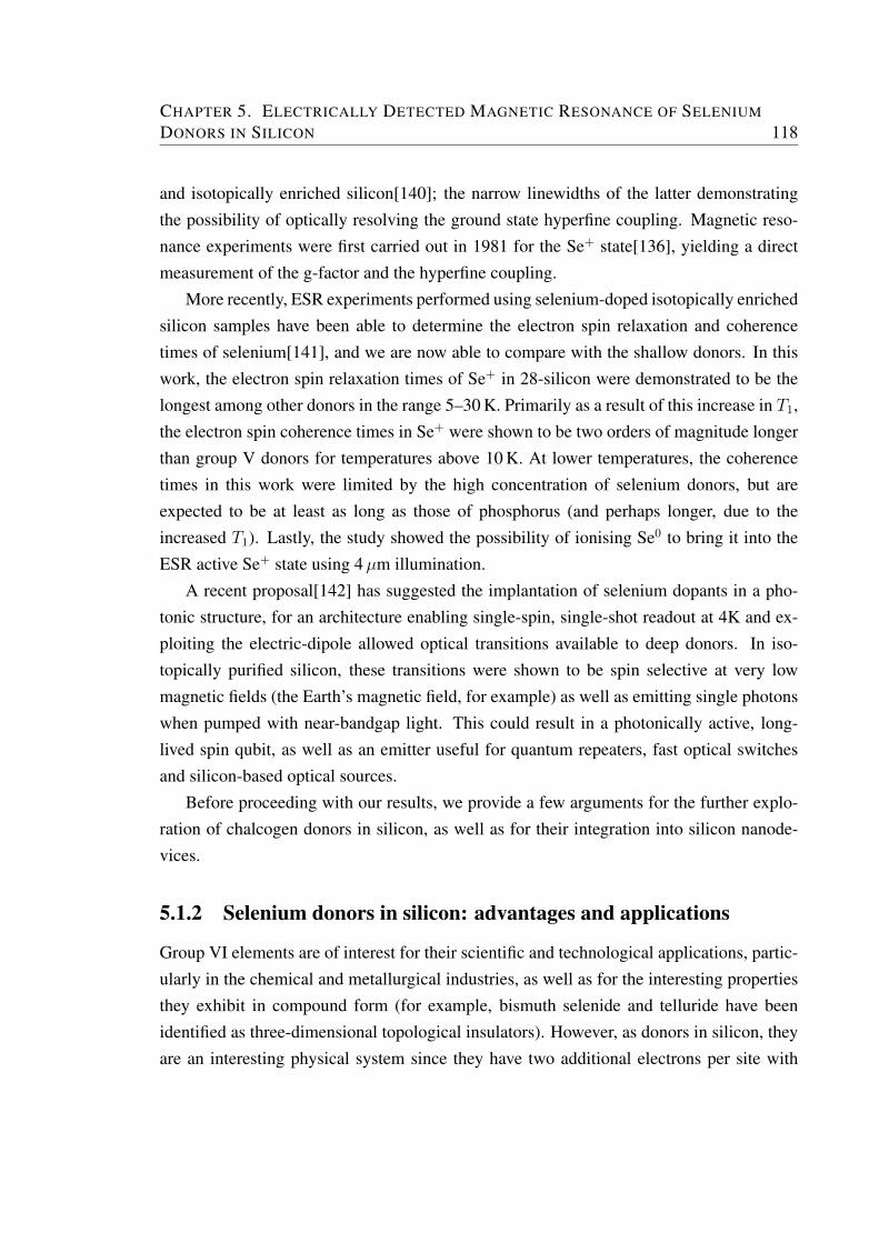
CHAPTER 5. ELECTRICALLY DETECTED MAGNETIC RESONANCE OF SELENIUM
DONORS IN SILICON 118
and isotopically enriched silicon[140]; the narrow linewidths of the latter demonstratingthe possibility of optically resolving the ground state hyperfine coupling. Magnetic reso-nance experiments were first carried out in 1981 for the Se+ state[136], yielding a directmeasurement of the g-factor and the hyperfine coupling.
More recently, ESR experiments performed using selenium-doped isotopically enrichedsilicon samples have been able to determine the electron spin relaxation and coherencetimes of selenium[141], and we are now able to compare with the shallow donors. In thiswork, the electron spin relaxation times of Se+ in 28-silicon were demonstrated to be thelongest among other donors in the range 5–30 K. Primarily as a result of this increase in T1,the electron spin coherence times in Se+ were shown to be two orders of magnitude longerthan group V donors for temperatures above 10 K. At lower temperatures, the coherencetimes in this work were limited by the high concentration of selenium donors, but areexpected to be at least as long as those of phosphorus (and perhaps longer, due to theincreased T1). Lastly, the study showed the possibility of ionising Se0 to bring it into theESR active Se+ state using 4µm illumination.
A recent proposal[142] has suggested the implantation of selenium dopants in a pho-tonic structure, for an architecture enabling single-spin, single-shot readout at 4K and ex-ploiting the electric-dipole allowed optical transitions available to deep donors. In iso-topically purified silicon, these transitions were shown to be spin selective at very lowmagnetic fields (the Earth’s magnetic field, for example) as well as emitting single photonswhen pumped with near-bandgap light. This could result in a photonically active, long-lived spin qubit, as well as an emitter useful for quantum repeaters, fast optical switchesand silicon-based optical sources.
Before proceeding with our results, we provide a few arguments for the further explo-ration of chalcogen donors in silicon, as well as for their integration into silicon nanode-vices.
5.1.2 Selenium donors in silicon: advantages and applications
Group VI elements are of interest for their scientific and technological applications, partic-ularly in the chemical and metallurgical industries, as well as for the interesting propertiesthey exhibit in compound form (for example, bismuth selenide and telluride have beenidentified as three-dimensional topological insulators). However, as donors in silicon, theyare an interesting physical system since they have two additional electrons per site with
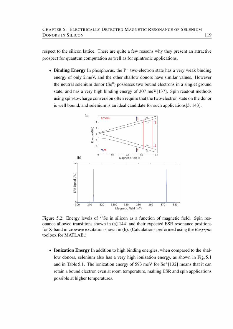
CHAPTER 5. ELECTRICALLY DETECTED MAGNETIC RESONANCE OF SELENIUM
DONORS IN SILICON 119
respect to the silicon lattice. There are quite a few reasons why they present an attractiveprospect for quantum computation as well as for spintronic applications.
• Binding Energy In phosphorus, the P− two-electron state has a very weak bindingenergy of only 2 meV, and the other shallow donors have similar values. Howeverthe neutral selenium donor (Se0) possesses two bound electrons in a singlet groundstate, and has a very high binding energy of 307 meV[137]. Spin readout methodsusing spin-to-charge conversion often require that the two-electron state on the donoris well bound, and selenium is an ideal candidate for such applications[5, 143].
2
-4
0
2
4
Magnetic Field (T)
Ener
gy (G
Hz)
0 0.1 0.2 0.3 0.4
9.7 GHz
3
4
2
1
mIme
Magnetic Field (mT)300 310 320 3300 330 350 360 370 380
EPR
Sign
al (A
U)
0
1.2
(a)
(b)
Figure 5.2: Energy levels of 77Se in silicon as a function of magnetic field. Spin res-onance allowed transitions shown in (a)[144] and their expected ESR resonance positionsfor X-band microwave excitation shown in (b). (Calculations performed using the Easyspintoolbox for MATLAB.)
• Ionization Energy In addition to high binding energies, when compared to the shal-low donors, selenium also has a very high ionization energy, as shown in Fig. 5.1and in Table 5.1. The ionization energy of 593 meV for Se+[132] means that it canretain a bound electron even at room temperature, making ESR and spin applicationspossible at higher temperatures.
CHAPTER 5. ELECTRICALLY DETECTED MAGNETIC RESONANCE OF SELENIUM
DONORS IN SILICON 120
• Spin Relaxation The spin relaxation time T1 of selenium was predicted (and mea-sured in an earlier work[141], as described in the previous section) to be extremelylong due to the large energy separation between the donor ground state and first ex-cited valley state. This energy splitting is an order of magnitude larger in Se+ thanfor group V donors in silicon. In 31P, this splitting is small (∆=10.5 meV)[145], lead-ing to phonon scattering being able to cause relaxation. This causes a rapid drop inT1 after a certain temperature, where the Raman process switches over to the Orbachprocess[146][147]. However, since Se has such a large splitting (∆=429 meV), thiseffectively removes the Orbach two-phonon spin relaxation mechanism (though itseffect on the strength of the Raman process is not fully understood yet), eliminatingthe sharp drop in T1 after a certain temperature. Indeed, the T1 measured in Ref. [141]follows the Raman process for 8 orders of magnitude and a huge range of tempera-tures. This is particularly useful for reaching higher operating temperatures for qubitor spintronics applications, and is promising for the electron spin coherence time T2,since T1 has been shown to limit T2 in the shallow donors.
Donor Group S I Ed (meV) g A (MHz) Reference31P V 1/2 1/2 45.6 1.9992 117.53 [131]
75As V 1/2 3/2 53.8 1.99837 198.35 [148]121Sb V 1/2 5/2 42.7 2.0004 186.8 [149]209Bi V 1/2 9/2 71.0 2.0003 1475.4 [150]33S0 VI 0 3/2 318 2.0054 - [136]33S+ VI 1/2 3/2 612 2.0054 312.4 [136]77Se0 VI 0 1/2 307 2.0057 - [136]77Se+ VI 1/2 1/2 589 2.0057 1658.5 [136]125Te0 VI 0 1/2 199 2.0023 - [136]125Te+ VI 1/2 1/2 411 2.0023 3491.7 [136]
Table 5.1: Experimental values of ionization energies, g-factors, and hyperfine interactionsfor shallow and deep donors in silicon.
• Electron Spin Coherence Times Directly as a result of the increase in the T1 (whichin shallow donors is a limiting factor especially at higher temperatures), the electronspin coherence times in Se+ were shown to be significantly longer than for group Vdonors for temperatures above 10 K[141]. This trend should hold for lower temper-atures as well, given samples lower in selenium concentration (which was a leadingcontributor to decoherence in the work referenced).
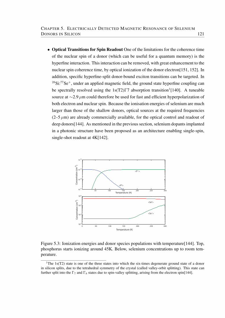
CHAPTER 5. ELECTRICALLY DETECTED MAGNETIC RESONANCE OF SELENIUM
DONORS IN SILICON 121
• Optical Transitions for Spin Readout One of the limitations for the coherence timeof the nuclear spin of a donor (which can be useful for a quantum memory) is thehyperfine interaction. This interaction can be removed, with great enhancement to thenuclear spin coherence time, by optical ionization of the donor electron[151, 152]. Inaddition, specific hyperfine-split donor-bound exciton transitions can be targeted. In28Si:77Se+, under an applied magnetic field, the ground state hyperfine coupling canbe spectrally resolved using the 1s(T2)Γ7 absorption transition1[140]. A tuneablesource at ∼2.9µm could therefore be used for fast and efficient hyperpolarization ofboth electron and nuclear spin. Because the ionisation energies of selenium are muchlarger than those of the shallow donors, optical sources at the required frequencies(2–5µm) are already commercially available, for the optical control and readout ofdeep donors[144]. As mentioned in the previous section, selenium dopants implantedin a photonic structure have been proposed as an architecture enabling single-spin,single-shot readout at 4K[142].
0 100 200 300
Temperature (K)50 150 250
<Se+>
<Se0>
1013
1014
1015
1016
Temperature (K)50 100 150 200 250 300
Conc
entra
tion
(cm
-3)
1013
1014
1015
1016
Conc
entra
tion
(cm
-3)
<P +>
<P0>
Figure 5.3: Ionization energies and donor species populations with temperature[144]. Top,phosphorus starts ionizing around 45K. Below, selenium concentrations up to room tem-perature.
1The 1s(T2) state is one of the three states into which the six-times degenerate ground state of a donorin silicon splits, due to the tetrahedral symmetry of the crystal (called valley-orbit splitting). This state canfurther split into the Γ7 and Γ8 states due to spin-valley splitting, arising from the electron spin[144].
CHAPTER 5. ELECTRICALLY DETECTED MAGNETIC RESONANCE OF SELENIUM
DONORS IN SILICON 122
In addition to these promising characteristics, selenium donors also have some positivefeatures that make them valuable for integration into nanodevices. As discussed in Chap-ter 1, this thesis is primarily concerned with the development and exploration of a hybriddopant-dot qubit and/or architecture and selenium is a viable candidate for this avenue ofresearch.
• Large Hyperfine Constant The hyperfine constants of shallow and deep donors insilicon are set out in Table 5.1. We immediately notice that selenium has one of thehighest hyperfine constants in the table (1.66 GHz), as well as having a nuclear spin-1/2 isotope, 77Se. One of our motivations to explore selenium as a dopant in siliconis for its integration into nanodevices, specifically the hybrid dopant-dot spin qubitin silicon that is the focus of this thesis. Such a qubit, where the dopant is selenium,would have a singlet-triplet mixing dominated by the hyperfine interaction with thenuclear spin localised at the donor site. The electron on the donor would then bedetuned by δ = AS · I, implying, for example, that in the case of phosphorus, witha hyperfine coupling strength of 117 MHz, the S(1,1)-T0 coherent evolution at a verylow exchange coupling could be driven at around 50 MHz[153]. For selenium, withits high hyperfine coupling of 1.66 GHz, the driving frequency could be much higher,in the GHz range (in addition to the relaxation and coherence time improvementsmentioned previously).
• Stark Shift The large value of ∆ for selenium should result in a highly reducedStark shift[154] when compared to shallow donors. This would be good news fornanodevice integration, since then the electron and nuclear spin coherence of Se+
would be relatively unaffected by the charge noise that is somewhat unavoidable ingate-controlled nanodevices (despite the large value of the hyperfine coupling).
Lastly, looking at Table 5.1, it is important to observe that there are two other deep, doubledonors available, selenium’s fellow chalcogens sulphur and tellurium. While these mayhave similar valuable properties to selenium (tellurium in particular has the highest hyper-fine constant of all the donors), we choose to focus on selenium. In the case of sulphur,there is no stable nuclear spin-1/2 isotope (and a much lower hyperfine splitting). For tel-lurium, we find a low solid solubility making it difficult to incorporate into substitutionalsites in silicon[155] (additionally, implantation-doped tellurium samples have shown con-flicting electronic properties, possibly due to implantation damage and the formation of
CHAPTER 5. ELECTRICALLY DETECTED MAGNETIC RESONANCE OF SELENIUM
DONORS IN SILICON 123
complex defects) or into the kind of samples studied in this thesis through ESR, EDMRor other nanodevice techniques. However, further research into these donors may well befruitful.
5.1.3 Spin-dependent transport mechanisms in silicon
Before discussing our results in their entirety, we look at a brief description of some com-mon spin-dependent transport processes in silicon. EDMR is a versatile technique thatcan elucidate many spin-dependent processes and spin-to-charge conversion mechanismsin silicon (indeed, sometimes one or more of these may be superimposed or competing).It is worthwhile to note that all these mechanisms have been explored and developed inthe context of shallow, single-electron donors in silicon (though some deep levels such asinterface traps have been studied). As such, more theoretical work is required to developa framework for the interpretation of charged, singly-ionised double donors in silicon withvery deep energy levels.
We look at broadly two kinds of models; (i) polarization-dependent models such asspin-dependent scattering, tunneling and trapping, where the carrier and paramagneticdefect polarizations influence the signal strength at resonance, and (ii) spin-pair mod-els, which use the concept of local donor-acceptor or donor-defect pairs to mediate spin-dependent recombination. The latter typically gives a higher EDMR signal, and the globalcarrier polarizations do not have much effect. However, in both these populations, themechanism involved is similar; under an applied magnetic field B0, paramagnetic defectsas well as photo-induced carriers will achieve equilibrium populations, resulting a certainvalue of the steady-state photocurrent. Upon resonant microwave irradiation, the thermalequilibrium population is destroyed as we flip the spin, and the singlet and triplet (or spinup and down) populations are equalised (assuming a saturated transition), giving a differentvalue of the steady state photocurrent and a peak (or dip) in the spectrum. We look at a fewEDMR mechanisms in brief below.
Bolometric detection
While not a spin-dependent transport mechanism in the typical sense, bolometric detec-tion, or changes in the conductivity due to resonant heating of the electrons in the sample,must be carefully ruled out as a primary mechanism. For bolometric heating, the signof the change in resistivity∆ρ at resonance is expected to follow the change in resistivity
CHAPTER 5. ELECTRICALLY DETECTED MAGNETIC RESONANCE OF SELENIUM
DONORS IN SILICON 124
with temperature δρ0/δT [86, 156]. Since we are operating at cryogenic temperatures, anytemperature dependence of the resistivity is caused by changes in the electron tempera-ture, since acoustic phonon scattering should not make a significant difference. In addition,a bolometric effect is expected to be enhanced at higher magnetic fields as the absorbedZeeman energy on resonance is increased.
Spin dependent trapping
Spin-dependent charge trapping occurs in the presence of paramagnetic traps, for instanceshallow donors in silicon at low temperature, which can be in the the neutral D0 state orthe doubly occupied D− state. For phosphorus, with a D0 ground state having a bindingenergy of 50meV, and a D− state with a very small binding energy of Eb ∼ 1−2 meV, therecan be no bound triplet states (unless at a very large magnetic field). Therefore, a D0 statecan capture a conduction electron if a donor spin in a triplet configuration with a conduc-tion electron is flipped (say during EDMR), so that they then form a singlet. Trapping ofconduction electrons decreases the current at resonance for shallow donors, since there arefewer photocarriers in the conduction band to contribute to the steady-state photocurrent.In the context of deep dopants like selenium, the binding energies are much higher than theshallow donors, and consequently the triplet states should not be forbidden. However, thesinglet-triplet capture rates may vary, with a measurable effect on the steady-state current.Currently this process is not well understood for deep, singly-ionised dopants like Se+ andhas not been observed to date, but we expect it to be quite different from the shallow donorcase (which have no bound triplet states).
Spin dependent tunneling and hopping
Spin-dependent tunneling is in principle similar to the trapping process, but the electronstunnel to localized paramagnetic states in a spin-dependent manner[157]. The tunnelingprobability of a conduction electron to a localised state, or between localised states in thecontext of spin-dependent hopping between adjacent singly occupied states, is determinedby the mutual spin orientation of the two participating spins. In the case of tunneling ontoa donor, the polarization of the charge carriers would matter. However for spin-dependenthopping, involving the hopping of conduction electrons from the conduction band tail be-tween donor pairs for instance, the relative spin states of the two dopants would matter, notthe conduction electron polarization. The current at resonance is expected to decrease for
CHAPTER 5. ELECTRICALLY DETECTED MAGNETIC RESONANCE OF SELENIUM
DONORS IN SILICON 125
tunneling processes, at least in the case of shallow donors, since electrons that can con-tribute to the photocurrent tunnel to donor states instead. The sign of the change in currentcan vary for a hopping process; for example, it has been shown to decrease at resonancefor interface defects such as Pb centers at high magnetic fields[158].
Spin-dependent scattering
Spin dependent scattering is a process that can occur without direct charge transfer (suchas the trapping or tunneling of an electron), since scattering events with paramagnetic cen-tres often have a spin dependence due to the scattering rates depending on the relativespin states. If the singlet or the triplet scattering cross sections are greater, the sample re-sistivity will change as a result. A detailed calculation in Ref. [159] has shown that thesinglet scattering cross section is expected to be greater, leading to an increase in sampleresistivity or a resonant decrease in current. However, this contradicts recent experimen-tal results[160][86] and theoretical work exists[161] showing that there can be cases witha higher triplet scattering cross section, which would lead to an increase in photocurrentat resonance. Lastly, since the effect is electron-polarization dependent (for instance, thechange in resistivity is proportional to the product of the donor and conduction electronpolarizations, for the case of scattering off neutral donors), we expect enhanced signals athigher magnetic fields.
Spin-dependent recombination
Spin dependent recombination was proposed by Kaplan, Solomon and Mott in 1978[162] toexplain the discrepancy in EDMR signal amplitudes between the current change of ∼10−6
expected from spin polarization based mechanisms and the current change of ∼10−2–10−4
detected in many EDMR experiments. Since then, especially for 31P-Pb centre experiments,spin dependent recombination through donor-defect or donor-acceptor pairs has become al-most synonymous with EDMR. Here, it is assumed that after the excitation of photocarriers,they recombine through mid-gap states, and singlet pairs recombine much faster than tripletpairs. The pairs do need to be in close proximity to facilitate a weak exchange interaction.Upon resonance, triplet pairs (which are slow to recombine) are converted to singlet pairs,which then recombine very fast, leading to a decrease in the current at resonance (as chargecarriers recombine and are depleted). In the KSM picture, global carrier polarizations donot play a role, leading to no polarization (and field) dependence of the EDMR signal.
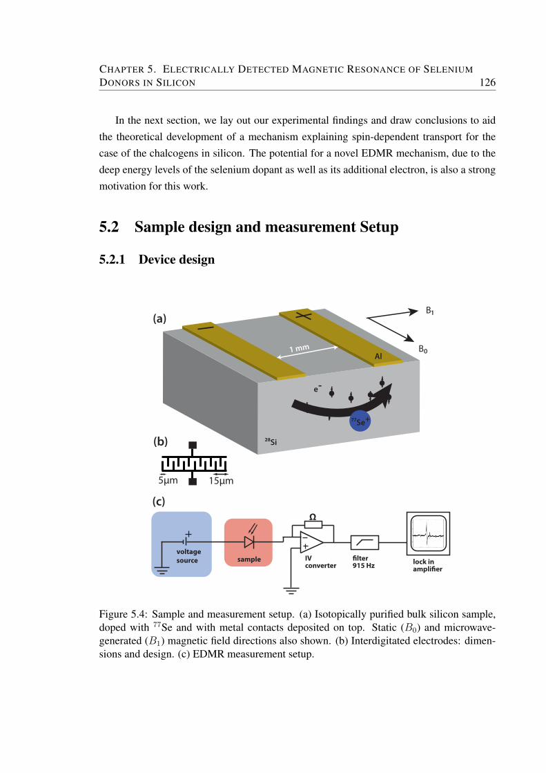
CHAPTER 5. ELECTRICALLY DETECTED MAGNETIC RESONANCE OF SELENIUM
DONORS IN SILICON 126
In the next section, we lay out our experimental findings and draw conclusions to aidthe theoretical development of a mechanism explaining spin-dependent transport for thecase of the chalcogens in silicon. The potential for a novel EDMR mechanism, due to thedeep energy levels of the selenium dopant as well as its additional electron, is also a strongmotivation for this work.
5.2 Sample design and measurement Setup
5.2.1 Device design
B
B
77Se+
28Si
e-
Al1 mm
voltage source sample IV
converterlter915 Hz lock in
amplier
Ω
(a)
(c)
(b)
15μm5μm
Figure 5.4: Sample and measurement setup. (a) Isotopically purified bulk silicon sample,doped with 77Se and with metal contacts deposited on top. Static (B0) and microwave-generated (B1) magnetic field directions also shown. (b) Interdigitated electrodes: dimen-sions and design. (c) EDMR measurement setup.
CHAPTER 5. ELECTRICALLY DETECTED MAGNETIC RESONANCE OF SELENIUM
DONORS IN SILICON 127
Device design for the measurement of spin-dependent transport, and EDMR in general,requires some careful consideration, since we are looking for a small change in current ontop of a large background which may itself change gradually with magnetic field (due to themagnetoresistance of doped silicon[163]). Current is typically measured through electrodesdeposited on the surface, and EDMR is very sensitive to surface impurities. As such, thesample surface must be kept extremely clean, especially before the contacts are deposited.Other device design constraints involve the shape and size of the contacts. Interdigitatedcontacts are chosen since they provide an improvement on the EDMR signal intensity byminimising absolute sample resistance and generating stronger local electric fields. Thedistance between the individual fingers of the contacts also needs to be taken into accountsince some EDMR mechanisms are length-dependent and will not occur on length scalesthat are too small. For our contacts, shown in Fig. 5.4(b), we chose an inter-digit distanceof 15µm, based on previous work[86].
Additionally, the bulk silicon sample itself and the dopant concentration needs to be op-timised. In our experiment, isotopically purified silicon was used to suppress decoherencearising from the 29Si nuclei (with nuclear spin 1/2), which occur with 5% natural abun-dance. In addition, as discussed previously, we are interested in the isotope of seleniumwith nuclear spin 1/2, 77Se. We also need an appreciable concentration of Se+ states, sinceit possesses a bound spin-1/2 electron and is ESR-active (in a previous study on the samesample showing good EPR signal intensities[141], the Se+ concentration was identified as∼4×1013 cm−3, which we should be able to detect through our EDMR experiment). Thisis achieved by doping with an acceptor, in our case boron.
The selenium doped devices used in this chapter were fabricated on samples preparedby M. Steger at Simon Fraser University[140]. The composition of the isotopically purifiedstarting material was 99.991% 28Si, with residual concentrations of 75 ppm 29Si and 15 ppm30Si. The boron concentration was∼5×1013 cm−3, confirmed by ESR measurements of theselenium spin relaxation T2[141]. Selenium was then thermally diffused into the sampleby sealing the silicon in an ampoule with the dopant at a temperature of 1000 K. Resistivitymeasurements were used to determine the concentration of selenium as ∼5×1015cm−3.This sample was infused with isotopically enriched selenium, with 97.1% concentration of77Se, the nuclear spin-1/2 isotope.
A schematic of the device used in this experiment is shown in Fig. 5.4(a). Interdigitatedcontacts (shown in Fig. 5.4(b); each finger is 5µm wide, with a spacing of 15µm betweenadjacent fingers, covering a 1 mm by 2 mm area on the sample surface) were fabricated by a
CHAPTER 5. ELECTRICALLY DETECTED MAGNETIC RESONANCE OF SELENIUM
DONORS IN SILICON 128
photolithographic lift-off procedure on the 28Si substrate, detailed in Appendix A. Prior tothis, the sample was put through a 10 minute deep solvent clean and a piranha etch followedby a plasma ash step to remove all metal, photoresist and organic residue, followed by a1 minute hydrofluoric acid wet treatment to remove native oxide. After photolithographicpattern development, 200 nm aluminium was deposited for the contacts through thermalevaporation. In EDMR measurements, a “dark current”, or a measurable value of currentthrough the sample while it is not illuminated, is typically associated with surface impuri-ties. In our sample, after the above treatment, the dark current went from a value close to10% of the off-resonance photocurrent to none (or rather, a value below the noise baselineof the apparatus, <0.01 % of the photocurrent). In addition, an array of lines in the EDMRspectrum typically associated with surface defects, complexes and/or contamination alsodisappeared completely (see Appendix A), leaving us with a strong selenium signal and abroad resonance centred around g = 2.
5.2.2 Measurement setup
Spin-dependent transport measurements require sensitive detection of current and typicallyrequire lock-in detection techniques. EDMR was carried out by continuous wave measure-ments (cw-EDMR) using a Bruker Elexsys spectrometer at X-band (9.7 GHz) around amagnetic field of 0.34 T. The sample was mounted on a PCB and wirebonded with 25µmaluminium wire on to each of the two interdigitated contacts. The PCB was then fittedinto an EDMR probe fitting into the Bruker spectrometer and lowered to be centered atthe static magnetic field, inside a cylindrical microwave resonator with a quality factortunable up to 20000 (tuned using a screw controlling the matching of the cavity and theamount of microwaves entering it, via the size of the coupling hole) and an inner diameterof 5 mm. The entire resonator was mounted within a liquid helium flow cryostat capable oftemperatures down to 4.2 K. The measurement setup is shown in Fig. 5.4(c). The photocur-rent required for EDMR was induced by white light generated by a xenon discharge lampcoupled in through a free-space optical window. The sample was biased with a constantvoltage source while the current from the sample was passed through an I-V converter andamplifier and a 915 Hz high-pass filter. Finally, using a lock-in amplifier, a component ofthe Bruker system, the signal from the sample was detected and demodulated. The mag-netic field is modulated by the lock-in amplifier modulation frequency, usually in the range10-100 kHz.
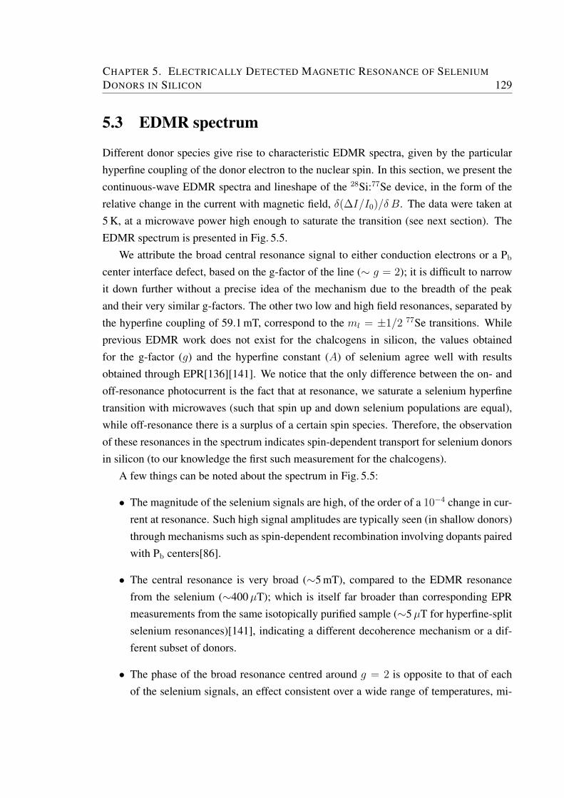
CHAPTER 5. ELECTRICALLY DETECTED MAGNETIC RESONANCE OF SELENIUM
DONORS IN SILICON 129
5.3 EDMR spectrum
Different donor species give rise to characteristic EDMR spectra, given by the particularhyperfine coupling of the donor electron to the nuclear spin. In this section, we present thecontinuous-wave EDMR spectra and lineshape of the 28Si:77Se device, in the form of therelative change in the current with magnetic field, δ(∆I/I0)/δ B. The data were taken at5 K, at a microwave power high enough to saturate the transition (see next section). TheEDMR spectrum is presented in Fig. 5.5.
We attribute the broad central resonance signal to either conduction electrons or a Pb
center interface defect, based on the g-factor of the line (∼ g = 2); it is difficult to narrowit down further without a precise idea of the mechanism due to the breadth of the peakand their very similar g-factors. The other two low and high field resonances, separated bythe hyperfine coupling of 59.1 mT, correspond to the ml = ±1/2 77Se transitions. Whileprevious EDMR work does not exist for the chalcogens in silicon, the values obtainedfor the g-factor (g) and the hyperfine constant (A) of selenium agree well with resultsobtained through EPR[136][141]. We notice that the only difference between the on- andoff-resonance photocurrent is the fact that at resonance, we saturate a selenium hyperfinetransition with microwaves (such that spin up and down selenium populations are equal),while off-resonance there is a surplus of a certain spin species. Therefore, the observationof these resonances in the spectrum indicates spin-dependent transport for selenium donorsin silicon (to our knowledge the first such measurement for the chalcogens).
A few things can be noted about the spectrum in Fig. 5.5:
• The magnitude of the selenium signals are high, of the order of a 10−4 change in cur-rent at resonance. Such high signal amplitudes are typically seen (in shallow donors)through mechanisms such as spin-dependent recombination involving dopants pairedwith Pb centers[86].
• The central resonance is very broad (∼5 mT), compared to the EDMR resonancefrom the selenium (∼400µT); which is itself far broader than corresponding EPRmeasurements from the same isotopically purified sample (∼5µT for hyperfine-splitselenium resonances)[141], indicating a different decoherence mechanism or a dif-ferent subset of donors.
• The phase of the broad resonance centred around g = 2 is opposite to that of eachof the selenium signals, an effect consistent over a wide range of temperatures, mi-
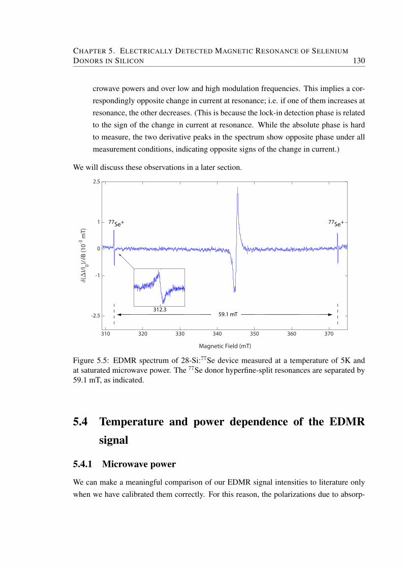
CHAPTER 5. ELECTRICALLY DETECTED MAGNETIC RESONANCE OF SELENIUM
DONORS IN SILICON 130
crowave powers and over low and high modulation frequencies. This implies a cor-respondingly opposite change in current at resonance; i.e. if one of them increases atresonance, the other decreases. (This is because the lock-in detection phase is relatedto the sign of the change in current at resonance. While the absolute phase is hardto measure, the two derivative peaks in the spectrum show opposite phase under allmeasurement conditions, indicating opposite signs of the change in current.)
We will discuss these observations in a later section.
312.3
77Se+ 77Se+
59.1 mT
Figure 5.5: EDMR spectrum of 28-Si:77Se device measured at a temperature of 5K andat saturated microwave power. The 77Se donor hyperfine-split resonances are separated by59.1 mT, as indicated.
5.4 Temperature and power dependence of the EDMRsignal
5.4.1 Microwave power
We can make a meaningful comparison of our EDMR signal intensities to literature onlywhen we have calibrated them correctly. For this reason, the polarizations due to absorp-
CHAPTER 5. ELECTRICALLY DETECTED MAGNETIC RESONANCE OF SELENIUM
DONORS IN SILICON 131
tion at resonance (p) have to be equal, and this is most easily achieved by measurementsat full saturation, so that p → 0. In this regime, the microwave power is sufficiently highsuch that the induced spin state transitions occur on a much faster timescale than the nat-ural relaxation rates. Then the spin up and spin down populations become equal; this iscalled the saturated state. The EDMR spectra and other measurements presented in thischapter are taken at saturation. We achieve this by increasing the microwave power untilthe EDMR signal intensity remains constant (Fig. 5.6(a)), indicating that the spin up anddown populations are equal.
A clear difference between conventional EPR and EDMR is the dependence of thesignal intensity on the microwave power[86][164]. A conventional EPR spectrum willhave a maximum signal intensity at a relatively low microwave power, as we see in theselenium EPR measurement in Fig. 5.6(b), followed by the signal dropping off again as themicrowave power (Pmw) is further increased. This behaviour follows the law
SEPR ∝ (1 + (1
4)γ2B2
1T1T2)−3/2(Pmw)1/2 (5.1)
while at high microwave powers, an inverse relation SEPR ∝ (Pmw)−1 is observed. Incontrast, for the EDMR power dependence, we have a high and constant signal reached atsaturation, as per the equation below:
SEDMR = CβPmw
1 + βPmw
(5.2)
where β and C are parameters, with C the saturation value at high Pmw. These predictionsare borne out in our experiment (the blue line in Fig. 5.6(a) is a fit to Eq. 5.2, while the onein Fig. 5.6(b) is a fit to Eq. 5.1), and throughout, we report EDMR signal intensities that aremaximised at saturation.
5.4.2 Linewidth and coherence time
EDMR lineshapes contain information about the spin relaxation times of the paramagneticspecies involved[83]. With inhomogeneous broadening, the cw-EPR linewidth exhibits aGaussian lineshape and provides information about T ∗2 only, while for intrinsic homoge-neous line broadening, Lorentzian functions fit well and the intrinsic T2 can be extracted.The principle is similar for EDMR lineshapes, and a peak to peak linewidth can be calcu-lated using the Bloch equations in the rotating frame[83], which give us the polarization in
CHAPTER 5. ELECTRICALLY DETECTED MAGNETIC RESONANCE OF SELENIUM
DONORS IN SILICON 132
(a) (b)
Microwave Power (mW)Microwave Power (mW)10-3 10-2 10-1 100 101
EPR
Sign
al (a
.u.)
x10-3
1
1.5
2
2.5
33.5
Figure 5.6: Power dependence of the EDMR and ESR resonances. (a) The power depen-dence of the EDMR signal with a fit (blue line) to Eq. 5.2. (b) The power dependenceof the EPR signal; the blue dashed line is a fit to Eq. 5.1 up to the saturation point (at amicrowave power of 0.1 mW), with the higher microwave power points fit to the inverserelation SEPR ∝ (Pmw)−1 as described in the main text.
terms of the magnetization. Combined with the fact that the EDMR signal is a change incurrent of the form[86]:
∆I
I0
=cpc
p0
[(1 + γ2T 2
2 (B0 −B)2
1 + γ2T 22 (B0 −B)2 + γ2B2
1T1T2
)2 − 1] (5.3)
where c is a constant representing the polarization-dependence of the carrier resistivity, andpc is the thermal equilibrium polarization of the carriers, we can take the derivative withrespect to B to obtain the measured EDMR lineshape. The peak-to-peak lineshape thenbecomes:
∆Bpp =1
3
1
γT 2[−12 + 18γ2B2
1T1T2 + 6√
16 + (3γ2B21T1T2)2]
12 (5.4)
In the limit of zero microwave power, when B1 → 0, this gives us:
∆Bpp =
√4
3
1
γT2
(5.5)
This equation for a homogeneously broadened line is derived within the confines of Lep-ine’s original polarization model[133] making it a crude measure of T2 for resonancesarising from more complex mechanisms (in such a case, pulsed-EDMR for a direct mea-
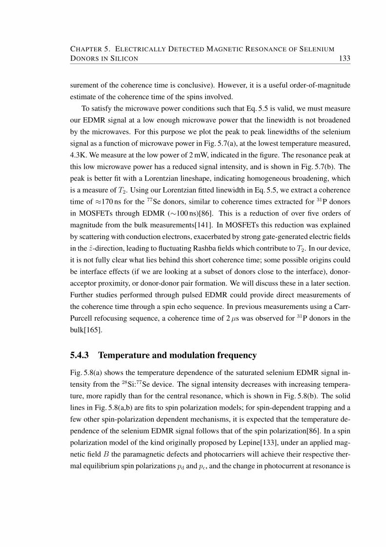
CHAPTER 5. ELECTRICALLY DETECTED MAGNETIC RESONANCE OF SELENIUM
DONORS IN SILICON 133
surement of the coherence time is conclusive). However, it is a useful order-of-magnitudeestimate of the coherence time of the spins involved.
To satisfy the microwave power conditions such that Eq. 5.5 is valid, we must measureour EDMR signal at a low enough microwave power that the linewidth is not broadenedby the microwaves. For this purpose we plot the peak to peak linewidths of the seleniumsignal as a function of microwave power in Fig. 5.7(a), at the lowest temperature measured,4.3K. We measure at the low power of 2 mW, indicated in the figure. The resonance peak atthis low microwave power has a reduced signal intensity, and is shown in Fig. 5.7(b). Thepeak is better fit with a Lorentzian lineshape, indicating homogeneous broadening, whichis a measure of T2. Using our Lorentzian fitted linewidth in Eq. 5.5, we extract a coherencetime of ≈170 ns for the 77Se donors, similar to coherence times extracted for 31P donorsin MOSFETs through EDMR (∼100 ns)[86]. This is a reduction of over five orders ofmagnitude from the bulk measurements[141]. In MOSFETs this reduction was explainedby scattering with conduction electrons, exacerbated by strong gate-generated electric fieldsin the z-direction, leading to fluctuating Rashba fields which contribute to T2. In our device,it is not fully clear what lies behind this short coherence time; some possible origins couldbe interface effects (if we are looking at a subset of donors close to the interface), donor-acceptor proximity, or donor-donor pair formation. We will discuss these in a later section.Further studies performed through pulsed EDMR could provide direct measurements ofthe coherence time through a spin echo sequence. In previous measurements using a Carr-Purcell refocusing sequence, a coherence time of 2µs was observed for 31P donors in thebulk[165].
5.4.3 Temperature and modulation frequency
Fig. 5.8(a) shows the temperature dependence of the saturated selenium EDMR signal in-tensity from the 28Si:77Se device. The signal intensity decreases with increasing tempera-ture, more rapidly than for the central resonance, which is shown in Fig. 5.8(b). The solidlines in Fig. 5.8(a,b) are fits to spin polarization models; for spin-dependent trapping and afew other spin-polarization dependent mechanisms, it is expected that the temperature de-pendence of the selenium EDMR signal follows that of the spin polarization[86]. In a spinpolarization model of the kind originally proposed by Lepine[133], under an applied mag-netic field B the paramagnetic defects and photocarriers will achieve their respective ther-mal equilibrium spin polarizations pd and pc, and the change in photocurrent at resonance is
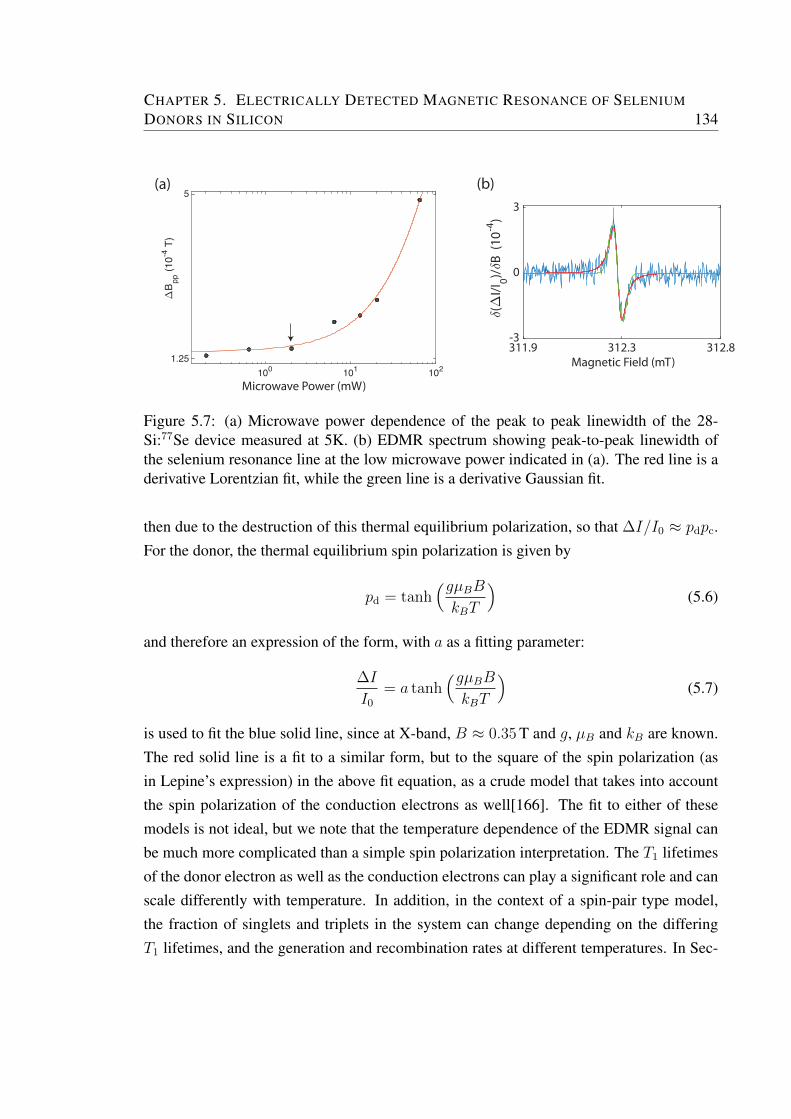
CHAPTER 5. ELECTRICALLY DETECTED MAGNETIC RESONANCE OF SELENIUM
DONORS IN SILICON 134
Microwave Power (mW)
(a) (b)
Magnetic Field (mT)
Figure 5.7: (a) Microwave power dependence of the peak to peak linewidth of the 28-Si:77Se device measured at 5K. (b) EDMR spectrum showing peak-to-peak linewidth ofthe selenium resonance line at the low microwave power indicated in (a). The red line is aderivative Lorentzian fit, while the green line is a derivative Gaussian fit.
then due to the destruction of this thermal equilibrium polarization, so that ∆I/I0 ≈ pdpc.For the donor, the thermal equilibrium spin polarization is given by
pd = tanh(gµBBkBT
)(5.6)
and therefore an expression of the form, with a as a fitting parameter:
∆I
I0
= a tanh(gµBBkBT
)(5.7)
is used to fit the blue solid line, since at X-band, B ≈ 0.35 T and g, µB and kB are known.The red solid line is a fit to a similar form, but to the square of the spin polarization (asin Lepine’s expression) in the above fit equation, as a crude model that takes into accountthe spin polarization of the conduction electrons as well[166]. The fit to either of thesemodels is not ideal, but we note that the temperature dependence of the EDMR signal canbe much more complicated than a simple spin polarization interpretation. The T1 lifetimesof the donor electron as well as the conduction electrons can play a significant role and canscale differently with temperature. In addition, in the context of a spin-pair type model,the fraction of singlets and triplets in the system can change depending on the differingT1 lifetimes, and the generation and recombination rates at different temperatures. In Sec-
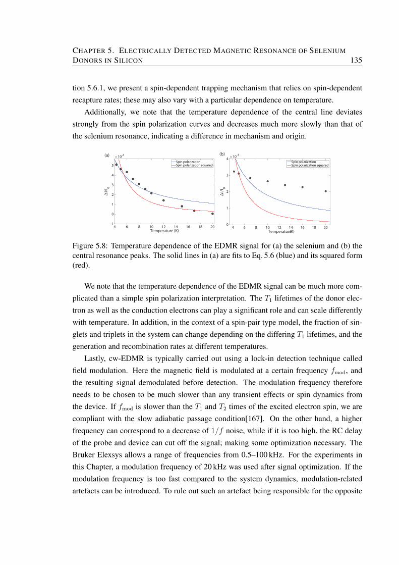
CHAPTER 5. ELECTRICALLY DETECTED MAGNETIC RESONANCE OF SELENIUM
DONORS IN SILICON 135
tion 5.6.1, we present a spin-dependent trapping mechanism that relies on spin-dependentrecapture rates; these may also vary with a particular dependence on temperature.
Additionally, we note that the temperature dependence of the central line deviatesstrongly from the spin polarization curves and decreases much more slowly than that ofthe selenium resonance, indicating a difference in mechanism and origin.
(a) (b)
(K)
Figure 5.8: Temperature dependence of the EDMR signal for (a) the selenium and (b) thecentral resonance peaks. The solid lines in (a) are fits to Eq. 5.6 (blue) and its squared form(red).
We note that the temperature dependence of the EDMR signal can be much more com-plicated than a simple spin polarization interpretation. The T1 lifetimes of the donor elec-tron as well as the conduction electrons can play a significant role and can scale differentlywith temperature. In addition, in the context of a spin-pair type model, the fraction of sin-glets and triplets in the system can change depending on the differing T1 lifetimes, and thegeneration and recombination rates at different temperatures.
Lastly, cw-EDMR is typically carried out using a lock-in detection technique calledfield modulation. Here the magnetic field is modulated at a certain frequency fmod, andthe resulting signal demodulated before detection. The modulation frequency thereforeneeds to be chosen to be much slower than any transient effects or spin dynamics fromthe device. If fmod is slower than the T1 and T2 times of the excited electron spin, we arecompliant with the slow adiabatic passage condition[167]. On the other hand, a higherfrequency can correspond to a decrease of 1/f noise, while if it is too high, the RC delayof the probe and device can cut off the signal; making some optimization necessary. TheBruker Elexsys allows a range of frequencies from 0.5–100 kHz. For the experiments inthis Chapter, a modulation frequency of 20 kHz was used after signal optimization. If themodulation frequency is too fast compared to the system dynamics, modulation-relatedartefacts can be introduced. To rule out such an artefact being responsible for the opposite
CHAPTER 5. ELECTRICALLY DETECTED MAGNETIC RESONANCE OF SELENIUM
DONORS IN SILICON 136
phase of the selenium and central resonances, we perform a modulation frequency study.Fig. 5.9 shows the selenium and central resonances taken at modulation frequencies of5 kHz, 20 kHz and 50 kHz, with no change in the relative phase between the two. In thefrequency range allowed by the Elexsys, we did not observe any change in this relativephase, and this, combined with the linewidth-extracted T2 of 170 ns ( 1/fmod) in theprevious section, leads us to conclude that our measurements are in the low-frequencylimit and consequently, fmod should not affect the signal.
-1
0
1
-1
0
1
-1
0
1
-1
0
1
312.2 312.8 313.4-1
0
1
340 345 350-1
0
1
Magnetic Field (mT)
EDM
R Si
gnal
(a.u
.)
5 kHz
20 kHz
50 kHz
Selenium Central
Figure 5.9: Temperature dependence of the EDMR signal for (a) the selenium and (b) thecentral resonance peaks.
5.5 Effects of laser and broad-wavelength illumination
Apart from the usual control parameters of temperature, microwave and field modulation,one way to study EDMR and identify its mechanism is to explore different illuminationsources to generate the photocurrent in the silicon. Previous studies[168] have explored thevariation in EDMR signals with white halogen light and lasers of different wavelengths;these variations were attributed to the fact that the optical penetration depth into silicon isstrongly wavelength dependent at cryogenic temperatures.
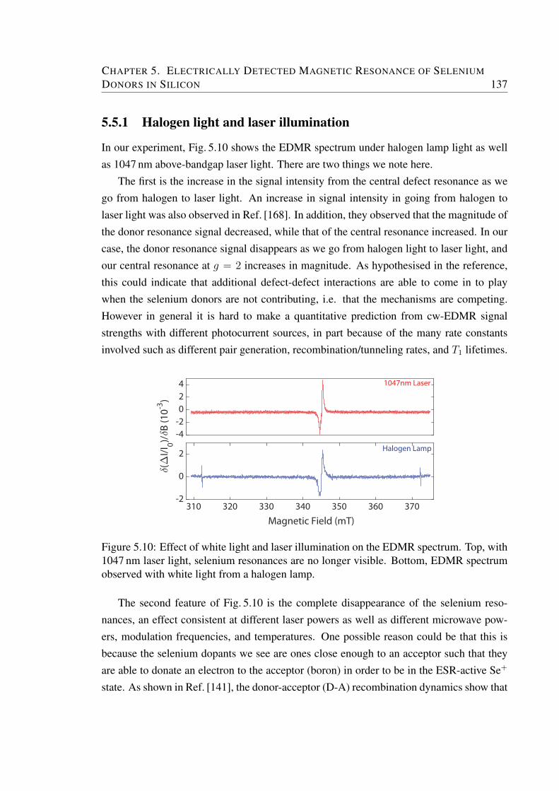
CHAPTER 5. ELECTRICALLY DETECTED MAGNETIC RESONANCE OF SELENIUM
DONORS IN SILICON 137
5.5.1 Halogen light and laser illumination
In our experiment, Fig. 5.10 shows the EDMR spectrum under halogen lamp light as wellas 1047 nm above-bandgap laser light. There are two things we note here.
The first is the increase in the signal intensity from the central defect resonance as wego from halogen to laser light. An increase in signal intensity in going from halogen tolaser light was also observed in Ref. [168]. In addition, they observed that the magnitude ofthe donor resonance signal decreased, while that of the central resonance increased. In ourcase, the donor resonance signal disappears as we go from halogen light to laser light, andour central resonance at g = 2 increases in magnitude. As hypothesised in the reference,this could indicate that additional defect-defect interactions are able to come in to playwhen the selenium donors are not contributing, i.e. that the mechanisms are competing.However in general it is hard to make a quantitative prediction from cw-EDMR signalstrengths with different photocurrent sources, in part because of the many rate constantsinvolved such as different pair generation, recombination/tunneling rates, and T1 lifetimes.
Halogen Lamp
1047nm Laser
Figure 5.10: Effect of white light and laser illumination on the EDMR spectrum. Top, with1047 nm laser light, selenium resonances are no longer visible. Bottom, EDMR spectrumobserved with white light from a halogen lamp.
The second feature of Fig. 5.10 is the complete disappearance of the selenium reso-nances, an effect consistent at different laser powers as well as different microwave pow-ers, modulation frequencies, and temperatures. One possible reason could be that this isbecause the selenium dopants we see are ones close enough to an acceptor such that theyare able to donate an electron to the acceptor (boron) in order to be in the ESR-active Se+
state. As shown in Ref. [141], the donor-acceptor (D-A) recombination dynamics show that
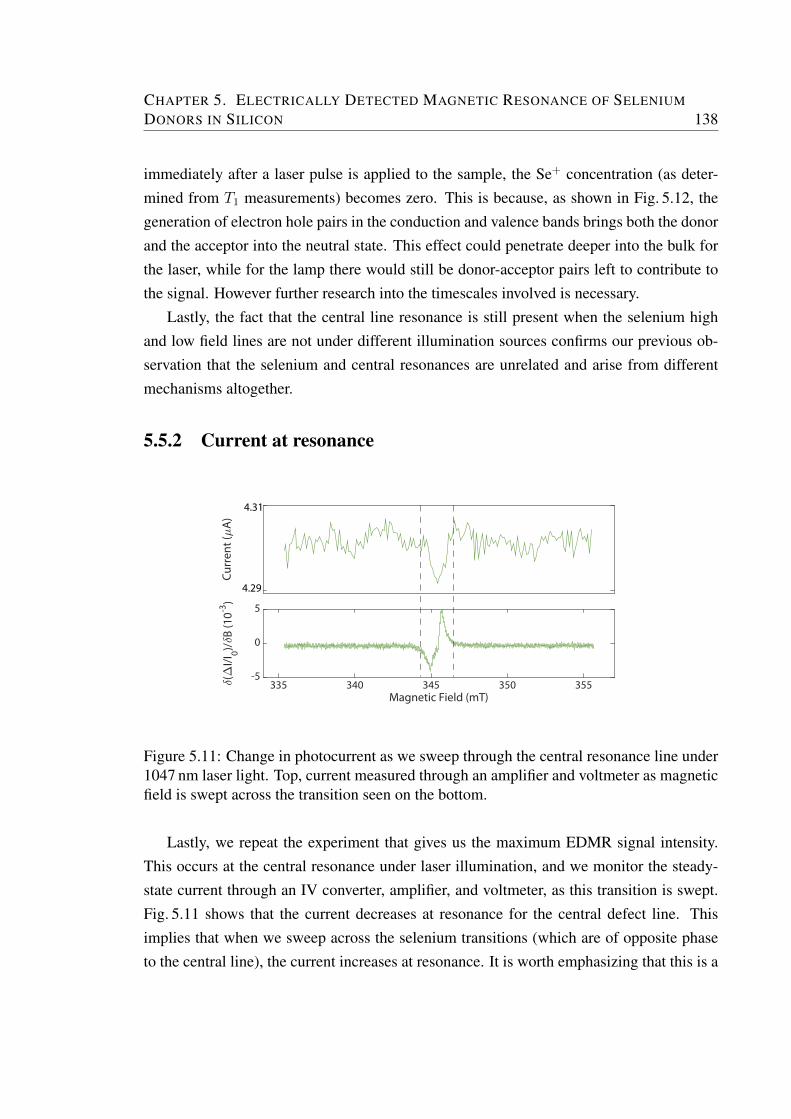
CHAPTER 5. ELECTRICALLY DETECTED MAGNETIC RESONANCE OF SELENIUM
DONORS IN SILICON 138
immediately after a laser pulse is applied to the sample, the Se+ concentration (as deter-mined from T1 measurements) becomes zero. This is because, as shown in Fig. 5.12, thegeneration of electron hole pairs in the conduction and valence bands brings both the donorand the acceptor into the neutral state. This effect could penetrate deeper into the bulk forthe laser, while for the lamp there would still be donor-acceptor pairs left to contribute tothe signal. However further research into the timescales involved is necessary.
Lastly, the fact that the central line resonance is still present when the selenium highand low field lines are not under different illumination sources confirms our previous ob-servation that the selenium and central resonances are unrelated and arise from differentmechanisms altogether.
5.5.2 Current at resonance
4.31
4.29
Figure 5.11: Change in photocurrent as we sweep through the central resonance line under1047 nm laser light. Top, current measured through an amplifier and voltmeter as magneticfield is swept across the transition seen on the bottom.
Lastly, we repeat the experiment that gives us the maximum EDMR signal intensity.This occurs at the central resonance under laser illumination, and we monitor the steady-state current through an IV converter, amplifier, and voltmeter, as this transition is swept.Fig. 5.11 shows that the current decreases at resonance for the central defect line. Thisimplies that when we sweep across the selenium transitions (which are of opposite phaseto the central line), the current increases at resonance. It is worth emphasizing that this is a
CHAPTER 5. ELECTRICALLY DETECTED MAGNETIC RESONANCE OF SELENIUM
DONORS IN SILICON 139
steady-state current, and should be interpreted as such; for a time-resolved picture, pulsedEDMR and careful monitoring of the current transients after the pulse should be used.
In the next section, we lay out our experimental findings and draw conclusions to aidthe theoretical development of a mechanism explaining the spin-dependent transport of thedouble donors in silicon.
5.6 Analysis
In this section we first summarize our experimental findings. First of all, we report the firstobservation, to our knowledge, of spin-dependent transport for a deep donor in silicon. Wemeasure this effect through EDMR and find a few interesting features in the spectra and inits dependence on various parameters.
First of all, the EDMR spectrum presented in Fig. 5.5 has a high signal amplitude(∆I/I ≈10−4) for the selenium hyperfine-split resonance peaks, and an even higher one(∆I/I ≈10−3) for the central resonance at g = 2. The width of the central peak is verybroad (∼5 mT), and that of the selenium peaks is two orders of magnitude broader than theESR linewidth measured from the same sample. By fitting a Lorentzian to the linewidth, wefind an approximate value of T2 ≈170 ns for the spin coherence time of the donors involvedin the spin-dependent transport process (five orders of magnitude lower than the bulk ESRvalue). Finally, the spectrum shows that the phase (and therefore the current change atresonance) of the central line is consistently opposite to that of the selenium transitions.
The power dependence of the EDMR signal is consistent with previous measurementsof EDMR from shallow donors, and we are able to saturate the EDMR transition by apply-ing enough microwave power (all results are reported in this regime). The contrast with thebehaviour of the EPR signal is also consistent with literature.
The temperature dependence of the EDMR signal (for the selenium and the central res-onance) shows a decrease with increasing temperature, and the selenium resonance showsa far stronger fit to spin polarization models than the central resonance.
We also perform the experiment with above band gap laser illumination (1047 nm) inaddition to the broadband white-light halogen lamp typically used in cw-EDMR. This ex-periment produces the interesting result that the central line is undiminished in intensity(indeed, the intensity increases) while the selenium resonances completely disappear, overa wide range of laser powers and even with all other factors, including the photocurrent,held constant.
CHAPTER 5. ELECTRICALLY DETECTED MAGNETIC RESONANCE OF SELENIUM
DONORS IN SILICON 140
Lastly, we observe that the photocurrent decreases at resonance for the central defectline, which implies that the photocurrent increases at resonance when we sweep across theselenium transitions (which are of opposite phase to the central line).
Selenium resonances and the central resonance
As a result of the experimental findings above, we conclude that the central defect reso-nance and the selenium resonances are not linked to each other nor part of the same spin-dependent process. We conclude this from the following facts: (a) the phases of the twosignals are opposite for all experimental parameters, and (b) the central resonance occursthrough a process which is roughly unchanged, except somewhat in intensity, by movingfrom a broadband white light source to above band gap illumination using a 1047 nm laserwhile the selenium resonances disappear (showing both that a different mechanism is atplay and that the central line is produced without being dependent on the selenium spinstate). Pb-only mechanisms such as spin dependent hopping have been proposed in situ-ations where spin dependent recombination is not dominant (at high magnetic fields, forinstance)[158] or where a suitable donor-defect recombination mechanism may not exist.We are concerned here with the mechanism of the spin dependent signal observed from thedeep donor, and we discuss this in the next section.
5.6.1 Mechanisms
The above experimental results are typically of great value in determining the spin-dependent transport mechanism operating for shallow donors in silicon. However, inthe case of deep, double donors in silicon, we lack a rigorous theoretical framework forthe evaluation of our results, and we also lack previous results in literature to compareagainst. We may perhaps only be able to eliminate some mechanisms through comparisonwith EDMR features seen when shallow donors are involved, and hazard a guess at theoperating mechanism. With these caveats, we go through the mechanisms presented inSection 5.1.3 below.
Bolometric heating
We are able to rule out bolometric heating for a few reasons. First, sample heating dueto the resonant ESR absorption of energy is considered to be negligible for phosphorus
CHAPTER 5. ELECTRICALLY DETECTED MAGNETIC RESONANCE OF SELENIUM
DONORS IN SILICON 141
concentrations in the ∼1015 cm−3 range[169]. In our sample, the total doping concentra-tion of selenium is ∼5×1015 cm−3 and the concentration of ESR-active single-ionised Se+
species is expected to be the same as the accceptor concentration, which is∼5×1013 cm−3.In addition, as discussed in the previous section, the sign of the change in resistivity ∆ρ
at resonance is expected to follow the change in resistivity with temperature δρ0/δT forbolometric heating. However, in our samples while the resistivity decreases at resonance(∆ρ/ρ0 < 0), the resistivity increases with increasing temperature (δρ0/δT > 0) in the nar-row range of temperatures 5–20 K. A bolometric effect is also expected to be enhanced athigher magnetic fields as the absorbed Zeeman energy on resonance is increased; we do notsee a difference in the selenium high and low field lines, which differ by 59.1 mT. Lastly,for a bolometric effect, the illumination source used to generate photocarriers (if photocur-rents and other parameters are kept constant) should not influence the EDMR signal, whilewe see a strong difference between laser and broadband light. However, we cannot rule outa bolometric mechanism for the central resonance.
Spin dependent scattering
As discussed in the previous section, scattering of conduction electrons from a donor spincan have a spin dependence from the different singlet triplet scattering cross sections. Inaddition, despite theoretical calculations to the contrary, resistivity decreases at resonance(i.e. an increase in current) have been reported, matching our experimental result. How-ever, the difference in scattering cross sections between singlet and triplet 2DEG-donorspin pairs are typically quite small and EDMR signal strengths in the 10−6 range are ex-pected, whereas ours are about two orders of magnitude higher. Also, a conduction electronsignal of the same phase as the selenium signal would conventionally be expected from ascattering mechanism, which we do not see.
Spin dependent recombination
Spin dependent recombination (SDR) is expected to yield EDMR signal intensities in thehigh range (∆I/I ≈10−2–10−4) that we measure, due to highly different recombinationrates for the singlet and triplet configurations of the donor-defect or donor-acceptor pairs.However, it is associated strongly with photocurrent quenching, which contradicts our cur-rent findings. However, there are studies involving less-studied defect pairs such as theoxygen vacancy center (OV−) in conjunction with phosphorus, which have observed a cur-
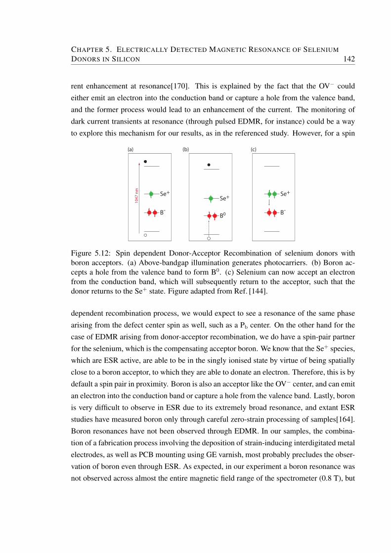
CHAPTER 5. ELECTRICALLY DETECTED MAGNETIC RESONANCE OF SELENIUM
DONORS IN SILICON 142
rent enhancement at resonance[170]. This is explained by the fact that the OV− couldeither emit an electron into the conduction band or capture a hole from the valence band,and the former process would lead to an enhancement of the current. The monitoring ofdark current transients at resonance (through pulsed EDMR, for instance) could be a wayto explore this mechanism for our results, as in the referenced study. However, for a spin
Se+
B-
Se+
B-
1047
nm
(a) (b)
B0
(c)
Se+
Figure 5.12: Spin dependent Donor-Acceptor Recombination of selenium donors withboron acceptors. (a) Above-bandgap illumination generates photocarriers. (b) Boron ac-cepts a hole from the valence band to form B0. (c) Selenium can now accept an electronfrom the conduction band, which will subsequently return to the acceptor, such that thedonor returns to the Se+ state. Figure adapted from Ref. [144].
dependent recombination process, we would expect to see a resonance of the same phasearising from the defect center spin as well, such as a Pb center. On the other hand for thecase of EDMR arising from donor-acceptor recombination, we do have a spin-pair partnerfor the selenium, which is the compensating acceptor boron. We know that the Se+ species,which are ESR active, are able to be in the singly ionised state by virtue of being spatiallyclose to a boron acceptor, to which they are able to donate an electron. Therefore, this is bydefault a spin pair in proximity. Boron is also an acceptor like the OV− center, and can emitan electron into the conduction band or capture a hole from the valence band. Lastly, boronis very difficult to observe in ESR due to its extremely broad resonance, and extant ESRstudies have measured boron only through careful zero-strain processing of samples[164].Boron resonances have not been observed through EDMR. In our samples, the combina-tion of a fabrication process involving the deposition of strain-inducing interdigitated metalelectrodes, as well as PCB mounting using GE varnish, most probably precludes the obser-vation of boron even through ESR. As expected, in our experiment a boron resonance wasnot observed across almost the entire magnetic field range of the spectrometer (0.8 T), but
CHAPTER 5. ELECTRICALLY DETECTED MAGNETIC RESONANCE OF SELENIUM
DONORS IN SILICON 143
this can by no means rule out boron as the other component of the spin pair. The decreasein the selenium EDMR signal strength as we increase the temperature could be caused bythe fact that boron typically has a short T1 which decreases rapidly with temperature.
Lastly, for a typical spin-dependent recombination mechanism as described in litera-ture, there is a pair formation between the donor and the acceptor where the photogener-ated electrons and holes are captured by the defect pairs (i.e. an electron by the seleniumand a hole by the boron). The pair can then recombine, with triplet recombination muchslower than singlet, leading to a spin permuation asymmetry observable through EDMR.Therefore, it is clear that a critical spin-selective process that differentiates between thesinglet and triplet states of the pair is required for SDR. The donor and acceptor speciesin our case are shown in Fig. 5.12. Here, if the Se+ donor state captures an electron, itleads to a neutral Se0 state such that there is no spin selectivity between the triplet and thesinglet. However, in part (b) of the figure we see that if the boron first accepts a hole fromthe valence band, we now have a spin pair composed of the Se+ and B0 states, and there isnow a spin-selective pathway, which leads to faster recombination in the case of a singletbeing formed.
Spin dependent hopping
We consider here another possible mechanism, that of spin-dependent hopping. This pro-cess in not fully understood in a general sense since it requires a detailed analysis of theparticular spin system under observation, to formulate a theory and predict experimentalbehaviour. Spin dependent hopping requires two singly occupied electron sites in closeproximity, for example a pair of singly ionised Se+ close to each other. Different processescan occur between the two sites, of which one or more has to be spin-dependent. Themodel is therefore similar to a spin pair model like spin dependent recombination, exceptthat in this case a spin dependent dissociation (and not recombination) destroys the pair,influencing transport rates and not the charge carrier density. Charge carriers do not anni-hilate during transport, in contrast to recombination; and so spin-dependent processes haveto be described in terms of mobility changes. There are models of spin dependent hoppingas well as experiments describing a current increase at resonance, however the transport,dynamics and hopping rate all depend on the specific pair.
For our experiment, this process is intriguing since we only see a selenium signal with-out a corresponding pair (and with a signal intensity higher than typical spin-dependentscattering processes), and a hopping model is possible with two selenium donors in prox-
CHAPTER 5. ELECTRICALLY DETECTED MAGNETIC RESONANCE OF SELENIUM
DONORS IN SILICON 144
imity. In addition, spin dependent hopping can lead to current increases at resonance,though a specific prediction for the case of a pair of deep double donors does not exist. Thehopping model might also explain the broad resonance and reduced coherence times of theEDMR species as compared to ESR data, since this is expected for paired donors close toeach other. Lastly, similar to SDR, this model also does not depend on a large conductionelectron polarization.
Indisputable experimental evidence of this kind of spin-dependent transport processwould be EDMR signals obtained under dark conditions. In the absence of excess chargecarriers, recombination does not exist and can be ruled out. A pulsed EDMR experimentwhere the dark current after the pulse is monitored would be useful.
Spin dependent trapping
We now consider a final possible EDMR mechanism. We mentioned earlier in this Chapterthat spin dependent trapping in shallow donors occurs due to the fact that bound tripletstates do not exist, such that a conduction electron can be trapped into a singlet configu-ration but not a triplet. But for deep donors like selenium in silicon, unlike the P− casefor a shallow donor like phosphorus, the two-electron charge state Se0 is indeed bound,and quite deeply (∼ 307 meV), as shown in Fig. 5.1. In our case, the new mechanism wepropose relies on the difference in the capture rates of the singlet and triplet states, formedby a conduction electron and the electron on the selenium atom in its Se+ state.
Off-resonance, the spin ensemble can have a different singlet/triplet content under con-stant illumination, due to differing recombination probabilites and T1 lifetimes. At reso-nance with the transition saturated with high microwave power, however, a random distri-bution of singlets and triplets is created. Depending on the electron capture rates for thesinglet and triplet configurations, then, there can be an appreciable difference in the steady-state current at resonance. If a certain species traps more conduction electrons, then due tothe reduction in its population at resonance (where the populations are equalised), there willbe more conduction electrons available and hence a resonant increase in the photocurrent,as we observe.
We present a simple rate-equation model below, where the photocurrent is determinedby the density of photoexcited electrons, I ∝ n(t). In this simpified picture of a trappingmechanism, there is a constant photocarrier generation rate kg due to the halogen illumina-
CHAPTER 5. ELECTRICALLY DETECTED MAGNETIC RESONANCE OF SELENIUM
DONORS IN SILICON 145
tion, and a constant recapture rate dependent on the dopant population, given by kcnd(t)
dn
dt= kg − kcnd(t) (5.8)
with kc the capture rate and nd the dopant population. The steady-state conduction electronpopulation (and a proportional photocurrent) is given by
nss =kg
kc
(5.9)
We now assume that the capture rate is spin-dependent, so that we have
dn
dt= kg − ksps − ktpt (5.10)
where ks and kt are the capture rates into the singlet and triplet configurations respectively,while ps and pt are the probabilities of projection into the singlet and triplet states for theselenium donor. For microwaves at resonance (with the transition saturated), ps = pt =
1/2. This will then give us the steady state electron number
nss =kg
ksps + ktpt
(5.11)
We are interested in the number of electrons in the steady states both on- and off-resonance, as this is proportional to the difference in the currents we measure. Defining thepolarization of the carriers as the fractional difference between the spin-up and spin-downpopulations, we have:
p =n↑ − n↓n↑ + n↓
, (5.12)
both for the donor and the conduction electrons. For the triplet state pt = p↑↑+p↓↓ we have
pt =(1 + pSe)(1 + pce) + (1− pSe)(1− pce)
4=
1 + pSepce
2(5.13)
CHAPTER 5. ELECTRICALLY DETECTED MAGNETIC RESONANCE OF SELENIUM
DONORS IN SILICON 146
and similarly, ps = 1−pSepce
2for the singlet state, where in both cases we have used the
expressions
p↓↓ =(1 + pSe)(1 + pce)
4
p↑↑ =(1− pSe)(1− pce)
4
(5.14)
and where pSe and pce are the spin polarizations of the donor and the conduction electrons,respectively.
For a simple calculation of the steady state difference in the capture rates ks and kt,therefore, we can consider the change in the number of electrons to be zero. We alsotake into account that the spin up and down populations of the selenium become equal atresonance for a saturated transition, leading to zero polarization. This gives us
nss(sat) =2kg
ks − kt
(5.15)
when the system is on resonance, using pSe = 0. Off-resonance, however, there is a dif-ference in the spin-up and down populations of the selenium and the differing populationsneed to be taken into account. For the off-resonance steady state, therefore, we have
nss =2kg
ks(1− pSepce) + kt(1 + pSepce)(5.16)
We can then obtain a ratio between the two steady-state conduction electron number values
nss(sat)
nss
= 1 + pSepce(1−2ks
ks + kt
) (5.17)
and therefore for our EDMR signal strength (the ratio of the current on and off resonance∆I/I0), in terms of the capture rates:
∆I
I0
=nss(sat)− nss
nss
= pSepce(kt − ks
kt + ks
) (5.18)
We can now estimate the difference in singlet and triplet capture rates required by ourmodel to match the experimental results:
kt
ks
=1 + c
1− c(5.19)
CHAPTER 5. ELECTRICALLY DETECTED MAGNETIC RESONANCE OF SELENIUM
DONORS IN SILICON 147
where c = ∆I/I0pSepce
. We calculate the donor spin polarisation pSe using Eq. 5.6 to be ∼ 5.5%.For the conduction electron polarization, as in the temperature dependence study (Section5.4.3), we assume the same form as the donor spin polarization (a valid assumption whenthe donor spins are in spin-lattice equilibrium, and also applicable when they are not if thecapture rates are faster than the spin-lattice relaxation[166]). This level of polarization ofthe donor and conduction electrons will then result in a required difference in the singletand triplet capture rates of 6%, i. e. a kt/ks ratio of around∼1.06. While we are not awareof direct measurements of capture rate differences for donors in silicon (which may partlybe because in the more intensively studied shallow donors, the triplet state is not bound andtherefore this EDMR mechanism does not exist), in other systems singlet-triplet capturerates can differ significantly. For instance, for deep trapping of conduction electrons in F-center (or colour center) defects in crystals, the range of ks/kt was found to be 4.4–38[171](noting that here the singlet capture rate is faster). Theoretical calculations of these capturerates will be a valuable resource in verifying our spin-dependent trapping mechanism.
5.6.2 Results and further work
In this chapter we presented the first observation, to our knowledge, of spin-dependenttransport in a deep donor in silicon. Electrically detected magnetic resonance was used toexplore the spin dependent transport mechanism in such devices. Temperature, microwavepower, steady-state current monitoring and different illumination sources were used to elu-cidate the features of the selenium resonances. The high signal strengths, reproduciblefeatures, and clear trends with temperature and illumination are all valuable pieces of in-formation and we look forward to a theoretical analysis that can pinpoint a mechanism forthe spin-dependent transport and spin-to-charge conversion we observe. In the previoussection, we have laid out a few mechanisms that are typically seen in silicon EDMR mea-surements and analysed our findings in each context. We have also presented a new EDMRmechanism possible in deep donors but not in their shallow counterparts; spin-dependenttrapping based on differing capture rates between the singlet and triplet configurations ofthe donor and conduction electron spins.
Further work would be useful to verify the transport mechanism and explore further thespin physics of deep donors in silicon, for spintronics and quantum information applica-tions. We hope to integrate selenium donors into single-dopant devices such as the ones
CHAPTER 5. ELECTRICALLY DETECTED MAGNETIC RESONANCE OF SELENIUM
DONORS IN SILICON 148
described in the next chapter and the EDMR results reported here are a valuable first stepin the understanding of deep donor physics in devices.
Some further measurements to perform would be, first, a careful monitoring of the cur-rent transient at resonance, especially in the dark. This is a possible way to rule out recom-bination in favour of spin-dependent transport processes. Secondly, using a few different il-lumination sources, such as lasers of different wavelengths (above-gap and sub-gap), wouldbe useful to determine the energy levels involved. EDMR studies carried out in lower con-centration samples would have fewer Se+ pairs in close proximity and this could reducethe signal strength if spin-dependent hopping were the underlying mechanism, yieldingvaluable information. High-magnetic fields (for instance, W-band EDMR)[156][86] havein the past shown interesting variations in mechanism for the shallow donors and will alsoprovide enhanced spectral resolution. Lastly, pulsed EDMR has been invaluable in study-ing the shallow donors in silicon, and the coherence and relaxation times of the subset ofdonors involved in spin-dependent transport. This would be welcome information in thecase of the deep donors as well in the context of device integration; it would shed light ontheir behaviour in the presence of electric fields and whether they retain their extremelylong ESR relaxation and coherence times.
Recent work also mentions the intriguing possibility of using the illumination sequencedeveloped in Ref. [141] (1047 nm + 4 m) to study the nuclear spin properties of neutralselenium (77Se0), a technique which requires the observation of EDMR. Our EDMR re-sults are the first steps towards such a process, which could be used to exploit the nuclearspin coherence time of neutral selenum (expected to be much longer even than Se+) by asequence consisting of manipulation followed by neutralization to preserve coherence.
Chapter 6
A Hybrid Dopant-Dot Double QuantumDot in Silicon
In this Chapter, we bring together the work presented in earlier chapters on quantum dotand dopant systems as well as the techniques developed to measure them. In Chapter 1, wediscussed the motivations behind the study of a coupled system consisting of quantum dotsand dopants in silicon. We noted the long coherence times of dopant electron and nuclearspins and their potential as quantum memories, and mentioned quantum computation archi-tectures consisting of quantum dots as processing units and spin buses to carry information.The common basic link between these proposals is a coherent coupling between a dopantand a quantum dot, in a scalable, compact architecture. In addition, there is scientific valuein the previously unexplored physics of the coupling between a natural atom (a phosphorusdonor) and an artificial atom (the quantum dot).
We now present measurements taken on a silicon nanowire transistor of the kind ex-plored as a quantum dot architecture in Chapter 4. The device presented here was designedand fabricated by the TOLOP project partners at CEA-Leti and measured at UCL at thebase temperature of our dilution fridge, as described in Chapter 3. We show now that givena version of the devices presented in Chapter 4, with the channel implanted at a dose corre-sponding to a few dopants in the channel, we are able to measure a coupled double quantumdot system made up of a single phosphorus atom and a corner quantum dot. This is to ourknowledge the first such measurement1.
1Recently, in a gate-defined metal-oxide-semiconductor quantum dot with a dopant implanted nearby,nuclear-spin driven singlet-triplet rotations were reported[30].
149
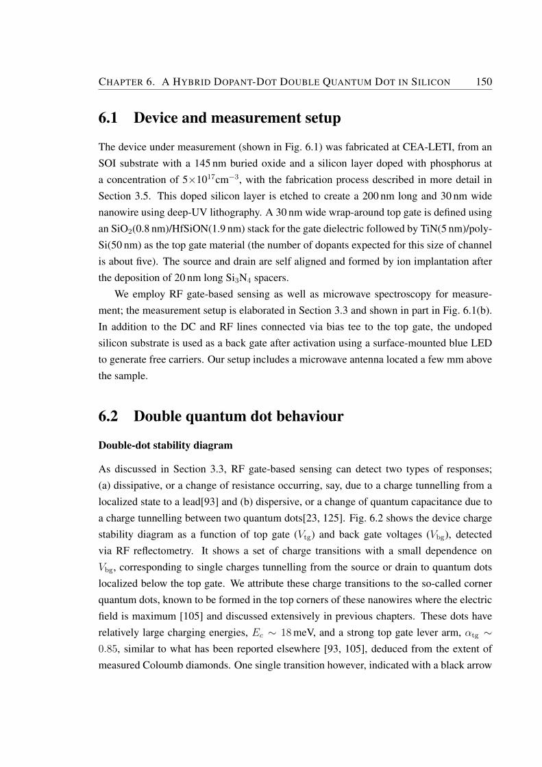
CHAPTER 6. A HYBRID DOPANT-DOT DOUBLE QUANTUM DOT IN SILICON 150
6.1 Device and measurement setup
The device under measurement (shown in Fig. 6.1) was fabricated at CEA-LETI, from anSOI substrate with a 145 nm buried oxide and a silicon layer doped with phosphorus ata concentration of 5×1017cm−3, with the fabrication process described in more detail inSection 3.5. This doped silicon layer is etched to create a 200 nm long and 30 nm widenanowire using deep-UV lithography. A 30 nm wide wrap-around top gate is defined usingan SiO2(0.8 nm)/HfSiON(1.9 nm) stack for the gate dielectric followed by TiN(5 nm)/poly-Si(50 nm) as the top gate material (the number of dopants expected for this size of channelis about five). The source and drain are self aligned and formed by ion implantation afterthe deposition of 20 nm long Si3N4 spacers.
We employ RF gate-based sensing as well as microwave spectroscopy for measure-ment; the measurement setup is elaborated in Section 3.3 and shown in part in Fig. 6.1(b).In addition to the DC and RF lines connected via bias tee to the top gate, the undopedsilicon substrate is used as a back gate after activation using a surface-mounted blue LEDto generate free carriers. Our setup includes a microwave antenna located a few mm abovethe sample.
6.2 Double quantum dot behaviour
Double-dot stability diagram
As discussed in Section 3.3, RF gate-based sensing can detect two types of responses;(a) dissipative, or a change of resistance occurring, say, due to a charge tunnelling from alocalized state to a lead[93] and (b) dispersive, or a change of quantum capacitance due toa charge tunnelling between two quantum dots[23, 125]. Fig. 6.2 shows the device chargestability diagram as a function of top gate (Vtg) and back gate voltages (Vbg), detectedvia RF reflectometry. It shows a set of charge transitions with a small dependence onVbg, corresponding to single charges tunnelling from the source or drain to quantum dotslocalized below the top gate. We attribute these charge transitions to the so-called cornerquantum dots, known to be formed in the top corners of these nanowires where the electricfield is maximum [105] and discussed extensively in previous chapters. These dots haverelatively large charging energies, Ec ∼ 18 meV, and a strong top gate lever arm, αtg ∼0.85, similar to what has been reported elsewhere [93, 105], deduced from the extent ofmeasured Coloumb diamonds. One single transition however, indicated with a black arrow
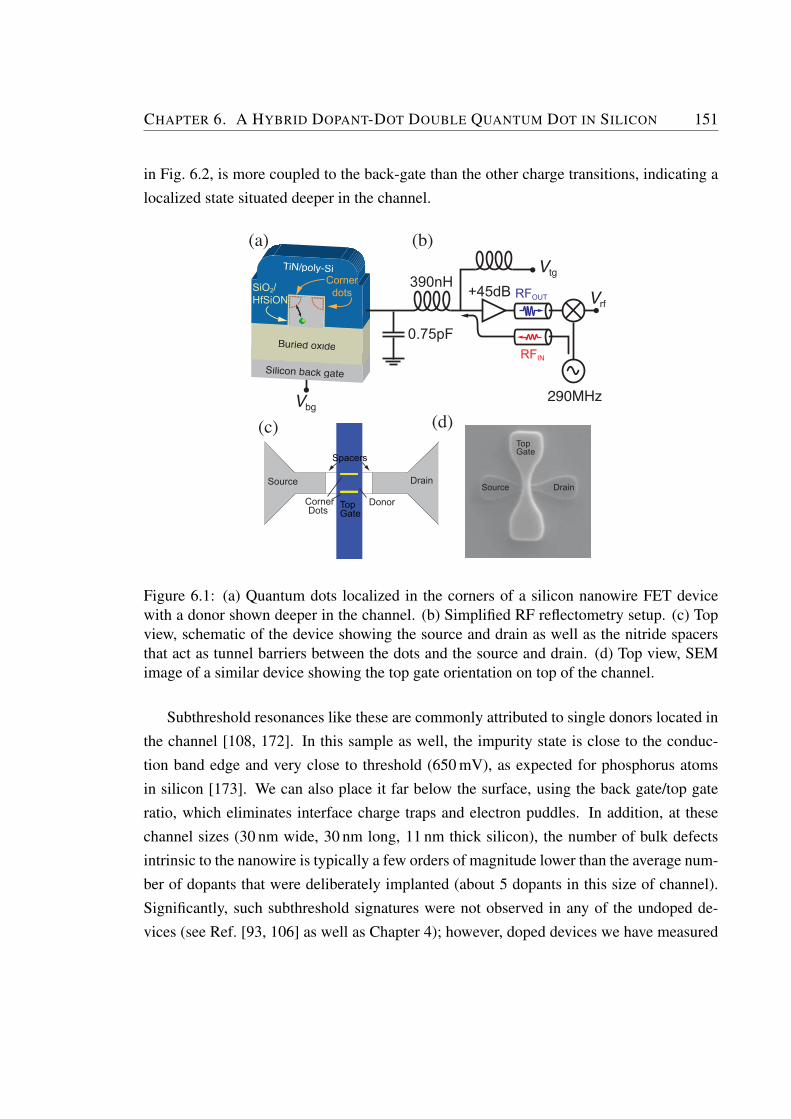
CHAPTER 6. A HYBRID DOPANT-DOT DOUBLE QUANTUM DOT IN SILICON 151
in Fig. 6.2, is more coupled to the back-gate than the other charge transitions, indicating alocalized state situated deeper in the channel.
(a) (b)
(c) (d)
RFIN
RFOUT
290MHz
+45dBVtg
Vrf
Vbg
0.75pF
390nHSiO2/HfSiON
Cornerdots
Source Drain
Top Gate
Spacers
Donor
Top Gate
Source DrainCornerDots
Figure 6.1: (a) Quantum dots localized in the corners of a silicon nanowire FET devicewith a donor shown deeper in the channel. (b) Simplified RF reflectometry setup. (c) Topview, schematic of the device showing the source and drain as well as the nitride spacersthat act as tunnel barriers between the dots and the source and drain. (d) Top view, SEMimage of a similar device showing the top gate orientation on top of the channel.
Subthreshold resonances like these are commonly attributed to single donors located inthe channel [108, 172]. In this sample as well, the impurity state is close to the conduc-tion band edge and very close to threshold (650 mV), as expected for phosphorus atomsin silicon [173]. We can also place it far below the surface, using the back gate/top gateratio, which eliminates interface charge traps and electron puddles. In addition, at thesechannel sizes (30 nm wide, 30 nm long, 11 nm thick silicon), the number of bulk defectsintrinsic to the nanowire is typically a few orders of magnitude lower than the average num-ber of dopants that were deliberately implanted (about 5 dopants in this size of channel).Significantly, such subthreshold signatures were not observed in any of the undoped de-vices (see Ref. [93, 106] as well as Chapter 4); however, doped devices we have measured
CHAPTER 6. A HYBRID DOPANT-DOT DOUBLE QUANTUM DOT IN SILICON 152
-0.1
0.0
0.1
dVrf/dV (a.u.)
Vbg (V)0 10
V tg (m
V)
600
620
640
660
680
5
Figure 6.2: The Gaussian filtered derivative of the demodulated resonator response as afunction of Vtg and Vbg (charge stability diagram). The black arrow indicates a chargetransition attributed to a phosphorus atom in the bulk of the nanowire.
regularly show such subthreshold resonances2, as do similar doped devices measured bydifferent research groups, as well as collaborators[108, 172](see also Appendix B for othermeasurements).
Quantum dot charge assignment
To correctly assign the electron filling of the DQD system to the transitions observed in thecharge stability diagram, we turn to the phase response of our resonator. We can extractthe phase response of the device from the I and Q channels. Fig. 6.3 shows the charge sta-bility diagram of the donor-dot system, with the phase response data plotted on the right.The signal intensity in a single channel does not vary enough to allow us to differentiatebetween the systems under study. However, the phase response data shows a strong varia-tion in intensity between the different quantum dots in the channel, most probably due todifferences in tunnel rates, as described in Section 3.3. The degree of visibility of its res-onances in the phase response should be characteristic of a particular quantum dot, sinceit is related to the proportion of its signal in the dissipative versus dispersive regimes (at
2Depending on channel length, about one in three doped devices will show such subthreshold resonancesthat are deeper in the channel and coupled more to the back gate, as opposed to those from corner dots.
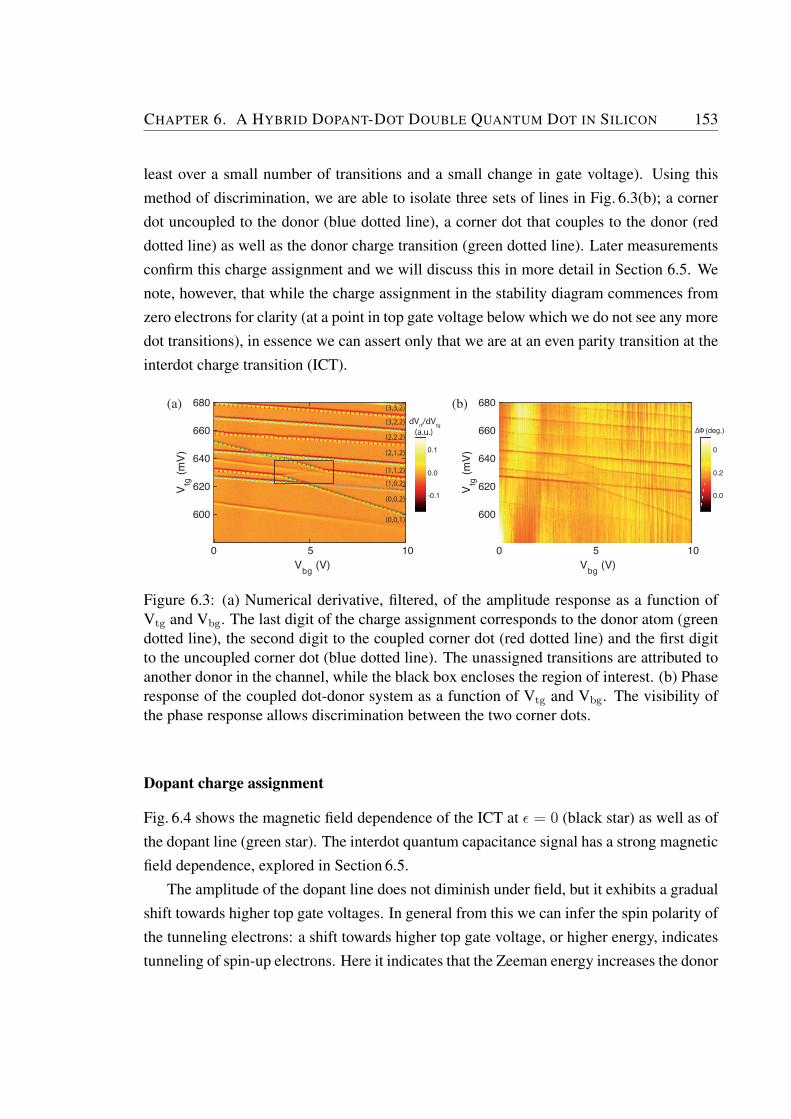
CHAPTER 6. A HYBRID DOPANT-DOT DOUBLE QUANTUM DOT IN SILICON 153
least over a small number of transitions and a small change in gate voltage). Using thismethod of discrimination, we are able to isolate three sets of lines in Fig. 6.3(b); a cornerdot uncoupled to the donor (blue dotted line), a corner dot that couples to the donor (reddotted line) as well as the donor charge transition (green dotted line). Later measurementsconfirm this charge assignment and we will discuss this in more detail in Section 6.5. Wenote, however, that while the charge assignment in the stability diagram commences fromzero electrons for clarity (at a point in top gate voltage below which we do not see any moredot transitions), in essence we can assert only that we are at an even parity transition at theinterdot charge transition (ICT).
-0.1
0.0
0.1
dVrf/dVtg (a.u.)
Vbg (V)0 10
V tg (m
V)
600
620
640
660
680
5
0.0
0.2
0
∆Φ (deg.)
Vbg (V)0 10
V tg (m
V)
600
620
640
660
680
5
(a) (b)
(0,0,2)
(1,0,2)
(1,1,2)
(2,1,2)
(2,2,2)
(3,2,2)
(3,3,2)
(0,0,1)
Figure 6.3: (a) Numerical derivative, filtered, of the amplitude response as a function ofVtg and Vbg. The last digit of the charge assignment corresponds to the donor atom (greendotted line), the second digit to the coupled corner dot (red dotted line) and the first digitto the uncoupled corner dot (blue dotted line). The unassigned transitions are attributed toanother donor in the channel, while the black box encloses the region of interest. (b) Phaseresponse of the coupled dot-donor system as a function of Vtg and Vbg. The visibility ofthe phase response allows discrimination between the two corner dots.
Dopant charge assignment
Fig. 6.4 shows the magnetic field dependence of the ICT at ε = 0 (black star) as well as ofthe dopant line (green star). The interdot quantum capacitance signal has a strong magneticfield dependence, explored in Section 6.5.
The amplitude of the dopant line does not diminish under field, but it exhibits a gradualshift towards higher top gate voltages. In general from this we can infer the spin polarity ofthe tunneling electrons: a shift towards higher top gate voltage, or higher energy, indicatestunneling of spin-up electrons. Here it indicates that the Zeeman energy increases the donor
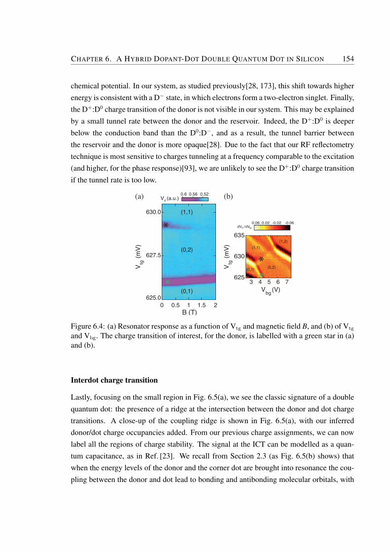
CHAPTER 6. A HYBRID DOPANT-DOT DOUBLE QUANTUM DOT IN SILICON 154
chemical potential. In our system, as studied previously[28, 173], this shift towards higherenergy is consistent with a D− state, in which electrons form a two-electron singlet. Finally,the D+:D0 charge transition of the donor is not visible in our system. This may be explainedby a small tunnel rate between the donor and the reservoir. Indeed, the D+:D0 is deeperbelow the conduction band than the D0:D−, and as a result, the tunnel barrier betweenthe reservoir and the donor is more opaque[28]. Due to the fact that our RF reflectometrytechnique is most sensitive to charges tunneling at a frequency comparable to the excitation(and higher, for the phase response)[93], we are unlikely to see the D+:D0 charge transitionif the tunnel rate is too low.
V tg (m
V)
627.5
630.0
B (T)0 0.5 1 1.5 2
0.520.560.6Vrf (a.u.)
625.0
(1,1)
(0,2)
(0,1)
625
630
635
-0.06-0.020.020.06dVrf /dVtg
(1,1)
(0,2)
(1,2)
(0,1)
76543
V tg (m
V)
Vbg (V)
(a) (b)
*
*
**
Figure 6.4: (a) Resonator response as a function of Vtg and magnetic field B, and (b) of Vtg
and Vbg. The charge transition of interest, for the donor, is labelled with a green star in (a)and (b).
Interdot charge transition
Lastly, focusing on the small region in Fig. 6.5(a), we see the classic signature of a doublequantum dot: the presence of a ridge at the intersection between the donor and dot chargetransitions. A close-up of the coupling ridge is shown in Fig. 6.5(a), with our inferreddonor/dot charge occupancies added. From our previous charge assignments, we can nowlabel all the regions of charge stability. The signal at the ICT can be modelled as a quan-tum capacitance, as in Ref. [23]. We recall from Section 2.3 (as Fig. 6.5(b) shows) thatwhen the energy levels of the donor and the corner dot are brought into resonance the cou-pling between the donor and dot lead to bonding and antibonding molecular orbitals, with
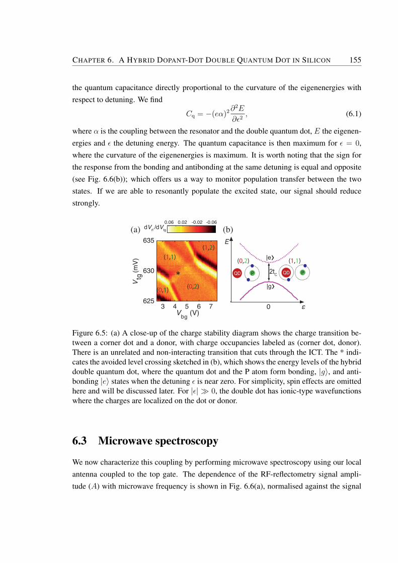
CHAPTER 6. A HYBRID DOPANT-DOT DOUBLE QUANTUM DOT IN SILICON 155
the quantum capacitance directly proportional to the curvature of the eigenenergies withrespect to detuning. We find
Cq = −(eα)2∂2E
∂ε2, (6.1)
where α is the coupling between the resonator and the double quantum dot, E the eigenen-ergies and ε the detuning energy. The quantum capacitance is then maximum for ε = 0,where the curvature of the eigenenergies is maximum. It is worth noting that the sign forthe response from the bonding and antibonding at the same detuning is equal and opposite(see Fig. 6.6(b)); which offers us a way to monitor population transfer between the twostates. If we are able to resonantly populate the excited state, our signal should reducestrongly.
E
2tCQD P
0 ε
QD P
(a) (b)
Vbg (V)3 4 5 6 7
Vtg
(mV)
625
630
635
-0.06-0.020.020.06dVrf /dVtg
|e›
|g›(0,2)
(1,1)
*
(1,2)
(0,1)
(0,2) (1,1)
Figure 6.5: (a) A close-up of the charge stability diagram shows the charge transition be-tween a corner dot and a donor, with charge occupancies labeled as (corner dot, donor).There is an unrelated and non-interacting transition that cuts through the ICT. The * indi-cates the avoided level crossing sketched in (b), which shows the energy levels of the hybriddouble quantum dot, where the quantum dot and the P atom form bonding, |g〉, and anti-bonding |e〉 states when the detuning ε is near zero. For simplicity, spin effects are omittedhere and will be discussed later. For |ε| 0, the double dot has ionic-type wavefunctionswhere the charges are localized on the dot or donor.
6.3 Microwave spectroscopy
We now characterize this coupling by performing microwave spectroscopy using our localantenna coupled to the top gate. The dependence of the RF-reflectometry signal ampli-tude (A) with microwave frequency is shown in Fig. 6.6(a), normalised against the signal
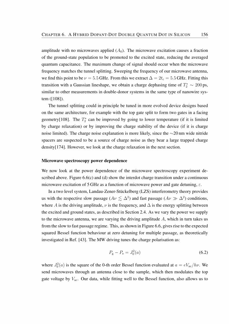
CHAPTER 6. A HYBRID DOPANT-DOT DOUBLE QUANTUM DOT IN SILICON 156
amplitude with no microwaves applied (A0). The microwave excitation causes a fractionof the ground-state population to be promoted to the excited state, reducing the averagedquantum capacitance. The maximum change of signal should occur when the microwavefrequency matches the tunnel splitting. Sweeping the frequency of our microwave antenna,we find this point to be ν = 5.5 GHz. From this we extract ∆ = 2tc = 5.5 GHz. Fitting thistransition with a Gaussian lineshape, we obtain a charge dephasing time of T ∗2 ∼ 200 ps,similar to other measurements in double-donor systems in the same type of nanowire sys-tem ([108]).
The tunnel splitting could in principle be tuned in more evolved device designs basedon the same architecture, for example with the top gate split to form two gates in a facinggeometry[108]. The T ∗2 can be improved by going to lower temperature (if it is limitedby charge relaxation) or by improving the charge stability of the device (if it is chargenoise limited). The charge noise explanation is more likely, since the ∼20 nm wide nitridespacers are suspected to be a source of charge noise as they bear a large trapped chargedensity[174]. However, we look at the charge relaxation in the next section.
Microwave spectroscopy power dependence
We now look at the power dependence of the microwave spectroscopy experiment de-scribed above. Figure 6.6(c) and (d) show the interdot charge transition under a continuousmicrowave excitation of 5 GHz as a function of microwave power and gate detuning, ε.
In a two level system, Landau-Zener-Stuckelberg (LZS) interferometry theory providesus with the respective slow passage (Aν . ∆2) and fast passage (Aν ∆2) conditions,where A is the driving amplitude, ν is the frequency, and ∆ is the energy splitting betweenthe excited and ground states, as described in Section 2.4. As we vary the power we supplyto the microwave antenna, we are varying the driving amplitude A, which in turn takes usfrom the slow to fast passage regime. This, as shown in Figure 6.6, gives rise to the expectedsquared Bessel function behaviour at zero detuning for multiple passage, as theoreticallyinvestigated in Ref. [43]. The MW driving tunes the charge polarisation as:
Pg − Pe = J20 (a) (6.2)
where J20 (a) is the square of the 0-th order Bessel function evaluated at a = eVac/hν. We
send microwaves through an antenna close to the sample, which then modulates the topgate voltage by Vac. Our data, while fitting well to the Bessel function, also allows us to
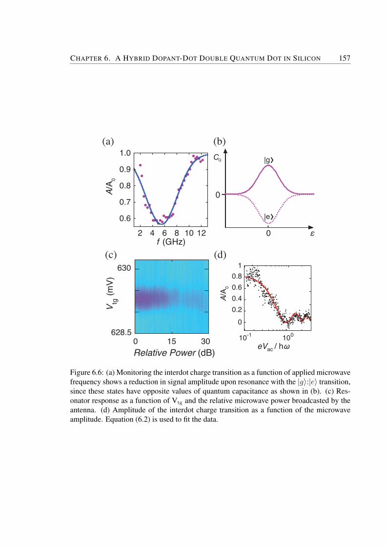
CHAPTER 6. A HYBRID DOPANT-DOT DOUBLE QUANTUM DOT IN SILICON 157
f (GHz)2 4 6 8 10 12
0.6
0.7
0.8
0.9
1.0
A/A 0
CQ
0
0 ε
(a) (b)
|e›
|g›
eVac / hω 10-1 100
00.20.40.60.8
1
A/A 0
(c) (d)
Relative Power (dB)0 15 30
V tg (m
V)
628.5
630
Figure 6.6: (a) Monitoring the interdot charge transition as a function of applied microwavefrequency shows a reduction in signal amplitude upon resonance with the |g〉:|e〉 transition,since these states have opposite values of quantum capacitance as shown in (b). (c) Res-onator response as a function of Vtg and the relative microwave power broadcasted by theantenna. (d) Amplitude of the interdot charge transition as a function of the microwaveamplitude. Equation (6.2) is used to fit the data.
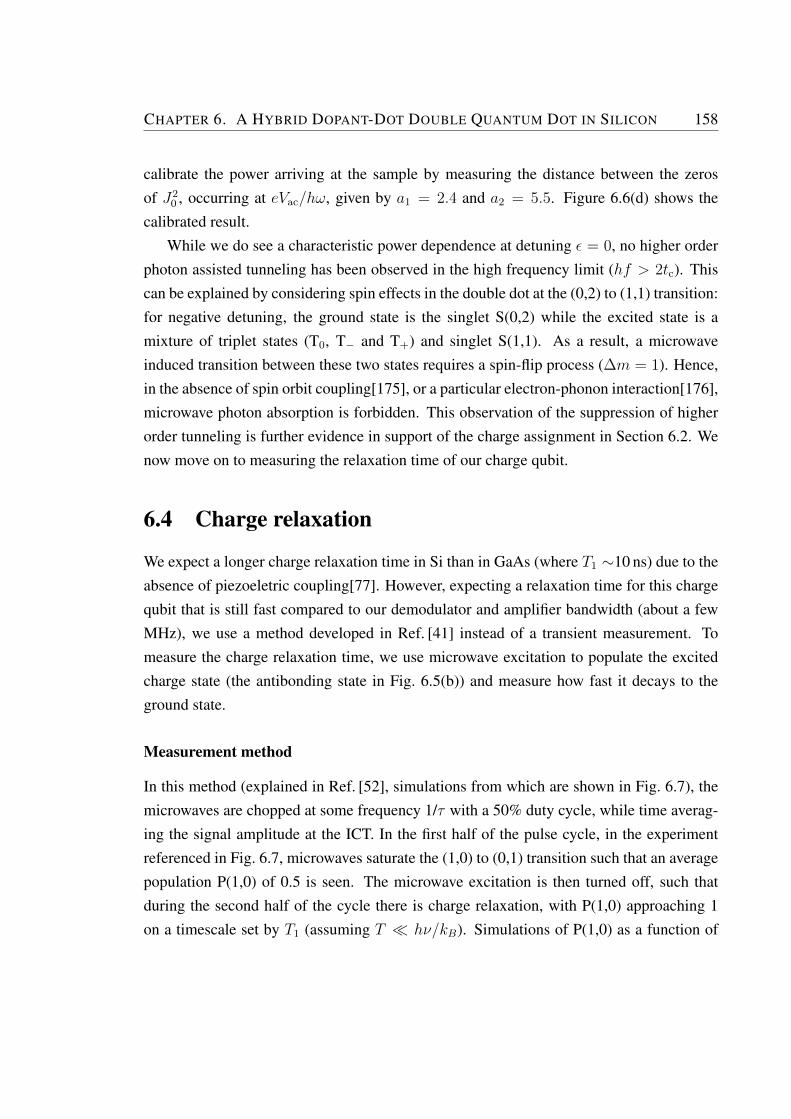
CHAPTER 6. A HYBRID DOPANT-DOT DOUBLE QUANTUM DOT IN SILICON 158
calibrate the power arriving at the sample by measuring the distance between the zerosof J2
0 , occurring at eVac/hω, given by a1 = 2.4 and a2 = 5.5. Figure 6.6(d) shows thecalibrated result.
While we do see a characteristic power dependence at detuning ε = 0, no higher orderphoton assisted tunneling has been observed in the high frequency limit (hf > 2tc). Thiscan be explained by considering spin effects in the double dot at the (0,2) to (1,1) transition:for negative detuning, the ground state is the singlet S(0,2) while the excited state is amixture of triplet states (T0, T− and T+) and singlet S(1,1). As a result, a microwaveinduced transition between these two states requires a spin-flip process (∆m = 1). Hence,in the absence of spin orbit coupling[175], or a particular electron-phonon interaction[176],microwave photon absorption is forbidden. This observation of the suppression of higherorder tunneling is further evidence in support of the charge assignment in Section 6.2. Wenow move on to measuring the relaxation time of our charge qubit.
6.4 Charge relaxation
We expect a longer charge relaxation time in Si than in GaAs (where T1 ∼10 ns) due to theabsence of piezoeletric coupling[77]. However, expecting a relaxation time for this chargequbit that is still fast compared to our demodulator and amplifier bandwidth (about a fewMHz), we use a method developed in Ref. [41] instead of a transient measurement. Tomeasure the charge relaxation time, we use microwave excitation to populate the excitedcharge state (the antibonding state in Fig. 6.5(b)) and measure how fast it decays to theground state.
Measurement method
In this method (explained in Ref. [52], simulations from which are shown in Fig. 6.7), themicrowaves are chopped at some frequency 1/τ with a 50% duty cycle, while time averag-ing the signal amplitude at the ICT. In the first half of the pulse cycle, in the experimentreferenced in Fig. 6.7, microwaves saturate the (1,0) to (0,1) transition such that an averagepopulation P(1,0) of 0.5 is seen. The microwave excitation is then turned off, such thatduring the second half of the cycle there is charge relaxation, with P(1,0) approaching 1on a timescale set by T1 (assuming T hν/kB). Simulations of P(1,0) as a function of
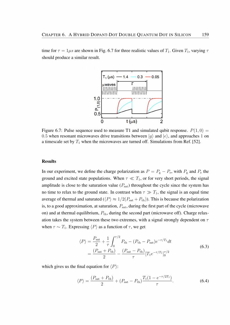
CHAPTER 6. A HYBRID DOPANT-DOT DOUBLE QUANTUM DOT IN SILICON 159
time for τ = 1µs are shown in Fig. 6.7 for three realistic values of T1. Given T1, varying τshould produce a similar result.
Figure 6.7: Pulse sequence used to measure T1 and simulated qubit response. P (1, 0) =0.5 when resonant microwaves drive transitions between |g〉 and |e〉, and approaches 1 ona timescale set by T1 when the microwaves are turned off. Simulations from Ref. [52].
Results
In our experiment, we define the charge polarization as P = Pg − Pe, with Pg and Pe theground and excited state populations. When τ T1, or for very short periods, the signalamplitude is close to the saturation value (Psat) throughout the cycle since the system hasno time to relax to the ground state. In contrast when τ T1, the signal is an equal timeaverage of thermal and saturated (〈P 〉 ≈ 1/2(Psat +Pth)). This is because the polarizationis, to a good approximation, at saturation, Psat, during the first part of the cycle (microwaveon) and at thermal equilibrium, Pth, during the second part (microwave off). Charge relax-ation takes the system between these two extremes, with a signal strongly dependent on τwhen τ ∼ T1. Expressing 〈P 〉 as a function of τ , we get
〈P 〉 =Psat
2+
1
τ
∫ τ/2
0
Pth − (Pth − Psat)e−τ/T1dt
=(Psat + Pth)
2− (Psat − Pth)
τ[T1e
−τ/T1 ]τ/20
(6.3)
which gives us the final equation for 〈P 〉:
〈P 〉 =(Psat + Pth)
2+ (Psat − Pth)
T1(1− e−τ/2T1)
τ. (6.4)
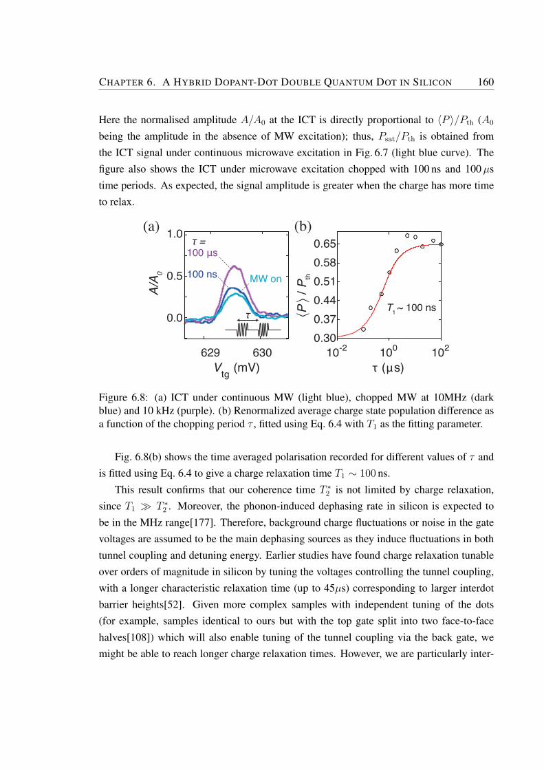
CHAPTER 6. A HYBRID DOPANT-DOT DOUBLE QUANTUM DOT IN SILICON 160
Here the normalised amplitude A/A0 at the ICT is directly proportional to 〈P 〉/Pth (A0
being the amplitude in the absence of MW excitation); thus, Psat/Pth is obtained fromthe ICT signal under continuous microwave excitation in Fig. 6.7 (light blue curve). Thefigure also shows the ICT under microwave excitation chopped with 100 ns and 100µstime periods. As expected, the signal amplitude is greater when the charge has more timeto relax.
τ (µs)10-2 100 102
0.300.370.440.510.580.65
(b)(a)
Vtg (mV)629 630
0.0
0.5
1.0
A/A 0
100 μs
100 ns MW on
τT1 ~ 100 ns〈P
〉 / P
th
τ =
Figure 6.8: (a) ICT under continuous MW (light blue), chopped MW at 10MHz (darkblue) and 10 kHz (purple). (b) Renormalized average charge state population difference asa function of the chopping period τ , fitted using Eq. 6.4 with T1 as the fitting parameter.
Fig. 6.8(b) shows the time averaged polarisation recorded for different values of τ andis fitted using Eq. 6.4 to give a charge relaxation time T1 ∼ 100 ns.
This result confirms that our coherence time T ∗2 is not limited by charge relaxation,since T1 T ∗2 . Moreover, the phonon-induced dephasing rate in silicon is expected tobe in the MHz range[177]. Therefore, background charge fluctuations or noise in the gatevoltages are assumed to be the main dephasing sources as they induce fluctuations in bothtunnel coupling and detuning energy. Earlier studies have found charge relaxation tunableover orders of magnitude in silicon by tuning the voltages controlling the tunnel coupling,with a longer characteristic relaxation time (up to 45µs) corresponding to larger interdotbarrier heights[52]. Given more complex samples with independent tuning of the dots(for example, samples identical to ours but with the top gate split into two face-to-facehalves[108]) which will also enable tuning of the tunnel coupling via the back gate, wemight be able to reach longer charge relaxation times. However, we are particularly inter-
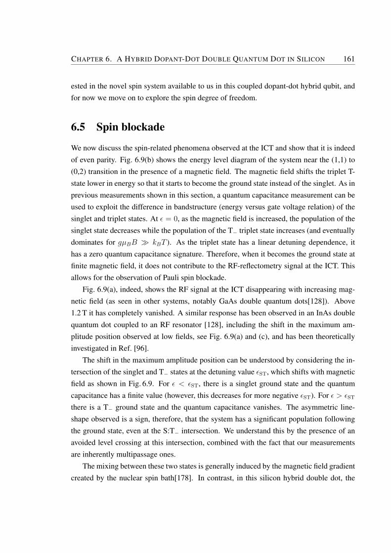
CHAPTER 6. A HYBRID DOPANT-DOT DOUBLE QUANTUM DOT IN SILICON 161
ested in the novel spin system available to us in this coupled dopant-dot hybrid qubit, andfor now we move on to explore the spin degree of freedom.
6.5 Spin blockade
We now discuss the spin-related phenomena observed at the ICT and show that it is indeedof even parity. Fig. 6.9(b) shows the energy level diagram of the system near the (1,1) to(0,2) transition in the presence of a magnetic field. The magnetic field shifts the triplet T-state lower in energy so that it starts to become the ground state instead of the singlet. As inprevious measurements shown in this section, a quantum capacitance measurement can beused to exploit the difference in bandstructure (energy versus gate voltage relation) of thesinglet and triplet states. At ε = 0, as the magnetic field is increased, the population of thesinglet state decreases while the population of the T− triplet state increases (and eventuallydominates for gµBB kBT ). As the triplet state has a linear detuning dependence, ithas a zero quantum capacitance signature. Therefore, when it becomes the ground state atfinite magnetic field, it does not contribute to the RF-reflectometry signal at the ICT. Thisallows for the observation of Pauli spin blockade.
Fig. 6.9(a), indeed, shows the RF signal at the ICT disappearing with increasing mag-netic field (as seen in other systems, notably GaAs double quantum dots[128]). Above1.2 T it has completely vanished. A similar response has been observed in an InAs doublequantum dot coupled to an RF resonator [128], including the shift in the maximum am-plitude position observed at low fields, see Fig. 6.9(a) and (c), and has been theoreticallyinvestigated in Ref. [96].
The shift in the maximum amplitude position can be understood by considering the in-tersection of the singlet and T− states at the detuning value εST, which shifts with magneticfield as shown in Fig. 6.9. For ε < εST, there is a singlet ground state and the quantumcapacitance has a finite value (however, this decreases for more negative εST). For ε > εST
there is a T− ground state and the quantum capacitance vanishes. The asymmetric line-shape observed is a sign, therefore, that the system has a significant population followingthe ground state, even at the S:T− intersection. We understand this by the presence of anavoided level crossing at this intersection, combined with the fact that our measurementsare inherently multipassage ones.
The mixing between these two states is generally induced by the magnetic field gradientcreated by the nuclear spin bath[178]. In contrast, in this silicon hybrid double dot, the
CHAPTER 6. A HYBRID DOPANT-DOT DOUBLE QUANTUM DOT IN SILICON 162
(b)
(a)
Vtg (mV)628.5 629.0 629.5
0.0
0.5
1.0
A/A 0
0 mT100 mT200 mT
(c)
V tg (m
V)
628
630
B (T)0 0.5 1 1.5 2
0.520.56Vrf (a.u.)
(1,1)
(0,2)
T+
S(0,2)
E
0 ε
T0 / S(1,1)
T-
S(0,2)
εST
gμB B
Figure 6.9: (a) The quantum capacitance signature of the interdot charge transition (ICT)become strongly suppressed with increasing magnetic field, as the T− triplet state becomesthe ground state, as shown in (b) the energy level diagram near the (1,1) to (0,2) transitionin the presence of a magnetic field. εST denotes the value at which the singlet and T− statesintersect, and is responsible for the shift and asymmetry observed in (c), the ICT measuredat 0 mT, 100 mT and 200 mT.
CHAPTER 6. A HYBRID DOPANT-DOT DOUBLE QUANTUM DOT IN SILICON 163
mixing should be dominated by the hyperfine interaction with the nuclear spin localizedat the donor site. As a result, neglecting the Overhauser field created by the 29Si, theelectron located on the donor is detuned by δ = AS · I where A is the hyperfine couplingconstant, S the electron spin and I the donor nuclear spin. We will discuss this mixing andits consequences in a later section.
6.6 Conclusions
To conclude, we have presented a hybrid double-dot system consisting of a phosphorusatom and a corner quantum dot in a foundry-fabricated nanoscale silicon transistor. First,this hybrid qubit is scalable by virtue of its implementation in an industry-compatible fab-rication platform. Secondly, the measurement of the double quantum dot is accomplishedwholly by the technique of gate-based reflectometry, which simplifies device fabricationand scaling up immensely, since a separate charge sensor quantum dot is not required. Wehave shown that both charge and spin effects in the system can be probed using this tech-nique, and in particular have measured coherence (T ∗2 ) and relaxation times for the chargequbit formed using microwave spectroscopy techniques.
Finally, the observation of spin blockade opens up ground for the exploration of spineffects in this novel, hybrid system as well as for a new kind of singlet-triplet qubit withspin dynamics possibly governed by the donor nuclear spin. This is hinted at by the avoidedlevel crossing formed by the mixing of the singlet and T− states which we attribute tothe hyperfine coupling of the electron with the nuclear spin of the phosphorus atom. Wediscussed before that the electron on the donor is detuned by the δ = AS · I where A is thehyperfine coupling constant, which for phosphorus is 117 MHz. Therefore the S(1,1)-T0
coherent evolution at a very low exchange coupling could be driven at ∼ 50 MHz. In thecase of bismuth, I = 9/2 and A = 1.48 GHz, the driving frequency should be even higherranging from 300 MHz up to 3 GHz depending on the nuclear spin state. Similarly, forselenium, the dopant explored in the previous Chapter 5, the hyperfine constant is similarlylarge, A = 1.66 GHz.
Finally, exploiting the interdot exchange coupling would allow a SWAP operation be-tween the corner dot and the donor atom spin state and, eventually, its storage in the donornuclear spin using electronuclear double-resonance (ENDOR) techniques. This would takeus one step closer to the qubit implementation mentioned at the beginning of the thesis
CHAPTER 6. A HYBRID DOPANT-DOT DOUBLE QUANTUM DOT IN SILICON 164
which enables the donor nuclear spin, with its extremely high coherence times, to be usedas a quantum memory.
6.7 Methods for coherent control
While we have presented spin effects in this hybrid dopant-dot system, ultimately the goalis to develop a coherent coupling that we can manipulate using microwaves, and use for thetransfer of information between the dopant and the dot. For this, the first step would be toperform electron spin resonance or ESR. In the previous section we saw that the quantumcapacitance signal has a finite curvature for the singlet state, and is flat in detuning forthe triplet state. This translates to a situation where the singlet gives us, via our coupledresonator, a strong signal at the ICT when we are in the singlet state, and no signal whenwe are in the T− triplet. This then provides us with a natural way of discrimination betweenthese two spin states of the system and we would like to be able to coherently evolve, oreven pulse between these two states.
As we have presented previously, in this system we were equipped with a static mag-netic field (used to bring the hybrid double-dot into spin blockade) as well as a microwaveantenna, built originally as a quarter-wave antenna for 20 GHz. In principle, this providesus with aB1 magnetic field orthogonal toB0, making ESR possible according to the princi-ples outlined in Chapter 3. However, in practice we were severely limited by the distance ofour antenna from the sample (a few mm) which meant that we were unable to apply the mi-crowave powers required to generate a magnetic field high enough to flip the spin, withoutheating up the dilution fridge. At moderate powers (at which the fridge temperature wasstable at a mixing chamber temperature lower than our measured electron temperature), wemeasured the amplitude of the RF signal with the double quantum dot in blockade, whileapplying microwaves at the frequency of the antenna, measured using a network analyserto be ∼19.4 GHz. Both methods of performing cw-ESR, i.e. sweeping the magnetic fieldwith the microwave frequency held constant, as well as sweeping the microwave frequencywith the field held constant, were employed. Our best-case results, after extensive signalfiltering and measurements taken over long timescales (spanning a day or so), are shownin Fig 6.10. In both cases, we saw a weak signal at points in field and frequency sepa-rated by the hyperfine splitting of phosphorus (117 MHz in frequency and 4.2 mT in field).While we stress that these measurements were inconclusive due to the high noise in themeasurement (as well as due to the fact that frequency vs magnetic field scans showing a
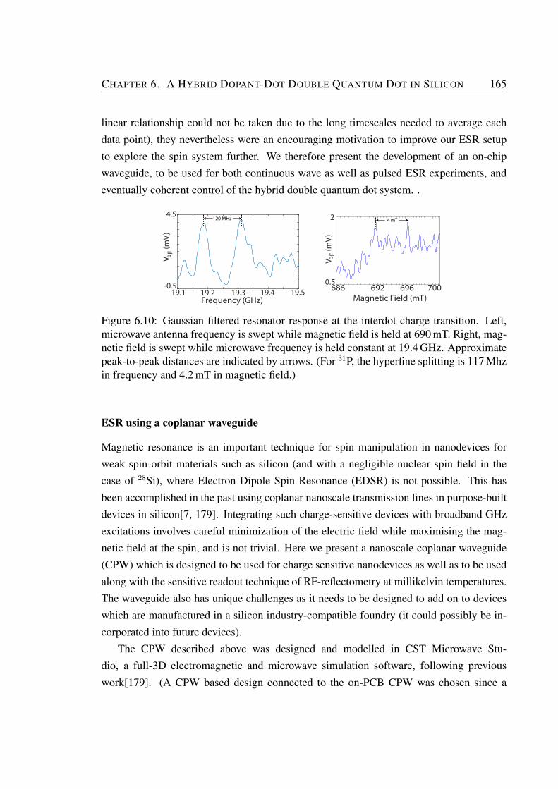
CHAPTER 6. A HYBRID DOPANT-DOT DOUBLE QUANTUM DOT IN SILICON 165
linear relationship could not be taken due to the long timescales needed to average eachdata point), they nevertheless were an encouraging motivation to improve our ESR setupto explore the spin system further. We therefore present the development of an on-chipwaveguide, to be used for both continuous wave as well as pulsed ESR experiments, andeventually coherent control of the hybrid double quantum dot system. .
Magnetic Field (mT)686 692 696 700
V RF (m
V)
0.5
2
19.1 19.2 19.4 19.519.3Frequency (GHz)
-0.5
4.5
V RF (m
V)
120 MHz 4 mT
Figure 6.10: Gaussian filtered resonator response at the interdot charge transition. Left,microwave antenna frequency is swept while magnetic field is held at 690 mT. Right, mag-netic field is swept while microwave frequency is held constant at 19.4 GHz. Approximatepeak-to-peak distances are indicated by arrows. (For 31P, the hyperfine splitting is 117 Mhzin frequency and 4.2 mT in magnetic field.)
ESR using a coplanar waveguide
Magnetic resonance is an important technique for spin manipulation in nanodevices forweak spin-orbit materials such as silicon (and with a negligible nuclear spin field in thecase of 28Si), where Electron Dipole Spin Resonance (EDSR) is not possible. This hasbeen accomplished in the past using coplanar nanoscale transmission lines in purpose-builtdevices in silicon[7, 179]. Integrating such charge-sensitive devices with broadband GHzexcitations involves careful minimization of the electric field while maximising the mag-netic field at the spin, and is not trivial. Here we present a nanoscale coplanar waveguide(CPW) which is designed to be used for charge sensitive nanodevices as well as to be usedalong with the sensitive readout technique of RF-reflectometry at millikelvin temperatures.The waveguide also has unique challenges as it needs to be designed to add on to deviceswhich are manufactured in a silicon industry-compatible foundry (it could possibly be in-corporated into future devices).
The CPW described above was designed and modelled in CST Microwave Stu-dio, a full-3D electromagnetic and microwave simulation software, following previouswork[179]. (A CPW based design connected to the on-PCB CPW was chosen since a
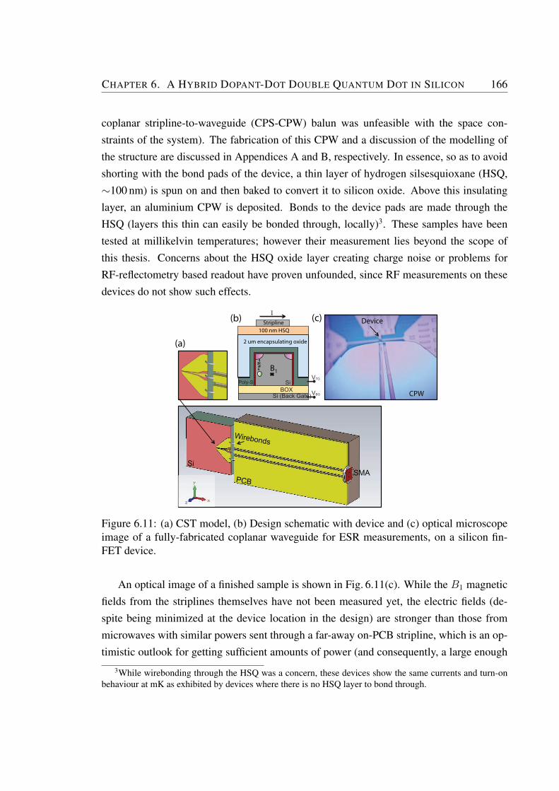
CHAPTER 6. A HYBRID DOPANT-DOT DOUBLE QUANTUM DOT IN SILICON 166
coplanar stripline-to-waveguide (CPS-CPW) balun was unfeasible with the space con-straints of the system). The fabrication of this CPW and a discussion of the modelling ofthe structure are discussed in Appendices A and B, respectively. In essence, so as to avoidshorting with the bond pads of the device, a thin layer of hydrogen silsesquioxane (HSQ,∼100 nm) is spun on and then baked to convert it to silicon oxide. Above this insulatinglayer, an aluminium CPW is deposited. Bonds to the device pads are made through theHSQ (layers this thin can easily be bonded through, locally)3. These samples have beentested at millikelvin temperatures; however their measurement lies beyond the scope ofthis thesis. Concerns about the HSQ oxide layer creating charge noise or problems forRF-reflectometry based readout have proven unfounded, since RF measurements on thesedevices do not show such effects.
Si
PCB SMA
Wirebonds
SiBOX
Si (Back Gate)
VTG
VBG
Poly-Si
Stripline
I
B1
2 um encapsulating oxide
100 nm HSQ
Device
CPW
(a)
(b) (c)
Figure 6.11: (a) CST model, (b) Design schematic with device and (c) optical microscopeimage of a fully-fabricated coplanar waveguide for ESR measurements, on a silicon fin-FET device.
An optical image of a finished sample is shown in Fig. 6.11(c). While the B1 magneticfields from the striplines themselves have not been measured yet, the electric fields (de-spite being minimized at the device location in the design) are stronger than those frommicrowaves with similar powers sent through a far-away on-PCB stripline, which is an op-timistic outlook for getting sufficient amounts of power (and consequently, a large enough
3While wirebonding through the HSQ was a concern, these devices show the same currents and turn-onbehaviour at mK as exhibited by devices where there is no HSQ layer to bond through.
CHAPTER 6. A HYBRID DOPANT-DOT DOUBLE QUANTUM DOT IN SILICON 167
oscillating magnetic field) to the spins in the sample. In future, given encouraging results,similar coplanar waveguides (or even micromagnets to provide a field gradient) could beintegrated into the silicon foundry fabrication protocol, ensuring a way of qubit control ina highly-scalable silicon architecture.
Operation as a singlet triplet qubit
Lastly, in the previous section, we presented another method of coherent control and spinqubit formation, motivated by the observation of a singlet-triplet (S(1,1)-T0) avoided cross-ing where the hyperfine coupling of the dopant nuclear spin could provide a magnetic fieldgradient to drive coherent spin rotations[153]. For this kind of system, we would not needan ESR microwave antenna, but simply fast voltage pulses to drive the transition as in atypical singlet-triplet qubit (EDSR)[66] as described in Section 2.5.2. This approach mer-its consideration of the RF-reflectometry drive which at the moment is always on duringqubit operation and readout. This is quite a large drive, chosen for signal-to-noise reasons(typically -85 dBm at the sample, though we have been able to go as low as -96 dBm) andcan have the effect of moving us over the entire transition in detuning, whereas we wouldlike to probe the (S(1,1)-T0) avoided crossing which has a very small extent in detuning,and requires a finer probe than this strong drive. The effect of the RF drive can possiblybe mitigated in a few ways. First, the drive amplitude could be reduced to much lowervalues, something that is possible by further engineering our RF-circuit and our cryogenicamplifiers, as well as reducing the noise in the measurement setup; or perhaps even by util-ising quantum-limited amplifiers such as a Josephson parametric amplifier (JPA). Secondly,qubit parameters such as the tunnel coupling could perhaps be tuned for a larger (S(1,1)-T0)avoided crossing in a different device geometry. Lastly, a fast (sub-nanosecond) switch forthe RF drive could be used to turn off the RF-drive during a pulse sequence, followed byturning it on for fast measurements taken at the zero detuning point (or elsewhere, depend-ing on the measurement protocol). This, combined with a reduced RF drive, could result ina viable hybrid dopant-dot singlet-triplet spin qubit.
Chapter 7
Conclusion and Outlook
In this Chapter, we summarize the work presented in this thesis in terms of the mainachievements in the development of dopant-dot qubits, and identify future directions forthe arenas of research presented. We give suggestions for improving the existing manipula-tion, readout and charge sensing techniques as well as the coherence properties of quantumdot and dopant spins in CMOS-compatible qubits, in the context of developing a scalablequantum computing architecture.
The main advancements presented in this thesis have been fourfold:
Gate-based reflectometry
In this thesis we have extensively used the technique of gate-based reflectometry for chargesensing of our few-electron quantum dots. This technique has recently gained a lot of pop-ularity and is especially suited to our edge-state quantum dots which have a very strongcoupling to the top gate, and hence to the resonator. In Chapter 4 we presented measure-ments which have developed this technique further for metrology applications and alongwith those in Chapter 6, have shown its applicability for the control and readout techniquesused for few-electron charge and spin qubits in silicon.
Firstly, in Chapter 4 we showed that similar to Coulomb blockade peaks for trans-port measurements, the dot-to-lead transition resonances detected through gate-based re-flectometry can be used to perform nanoscale thermometry, without the need for externalthermometers and integrated into a silicon-CMOS architecture. We also showed that thebehaviour of the resonance at low temperatures can also be used to extract tunnel rates ofthe quantum dot involved, which is valuable information for qubit tuning and control. Sec-
168
CHAPTER 7. CONCLUSION AND OUTLOOK 169
ondly, we performed microwave measurements on the dot-to-lead resonance and showedthat these can be used to calibrate the amount of microwave power arriving at the sam-ple. We developed a theory to simulate the peak splitting, and found that this method ofmicrowave calibration has potential to be used for pulse shape calibration as well.
Lastly, in Chapter 4 and 6 we showed that sensitive measurements of the charge andspin state of a double quantum dot can be performed using this gate-based charge sensor.We showed that the charge stability diagram of edge-state quantum dots as well as hybriddopant-dot systems can be measured with high bandwidth. The detection of Landau-Zenerinterferometry in multiple regimes through gate based reflectometry was demonstrated, aswell as Pauli spin blockade, both well established and essential techniques for the read-out and control of charge and spin qubits in quantum dots. This is a significant advancesince gate-based reflectometry can enable us to construct complex and close-packed qubitstructures without the need for external charge sensors.
CMOS foundry-based quantum dot architecture
Spin qubits in silicon have recently been shown to have excellent coherence characteris-tics and prospects for scalability[6–8, 17, 18]. Spin qubits in silicon, established mainlyin the planar-MOS process, have been proposed and also experimentally demonstrated inacademic laboratories, some of them high-fidelity qubits close to satisfying error correc-tion conditions. However, all of these approaches rely on external charge sensors of thesame scale as the device, as well as external, coplanar micromagnets or striplines for qubitcontrol.
In this thesis, we have made some first steps to show that similar high-fidelity spinqubits can be manufactured in silicon using industry-standard CMOS processes within alarge-scale nanofabrication facility with fabrication methods essentially identical to thatof the consumer electronics industry. In Chapters 4 and 6, we have shown that our ap-proach, based on a single, versatile building block (the wrap-around gate on SOI) can beimplemented in various configurations to form single and double quantum dots as well asa hybrid dopant-dot system. Some of the qubits that can be built using this basic scheme,with the wrap-around gate divided into two facing control gates, are shown in Fig. 7.1. Thisbuilding block can also be extended in the second dimension using nanowires facing eachother in close proximity. Furthermore, this kind of system can harbour low temperatureperipheral electronics, sharing the same CMOS tehnology and manufactured at the same
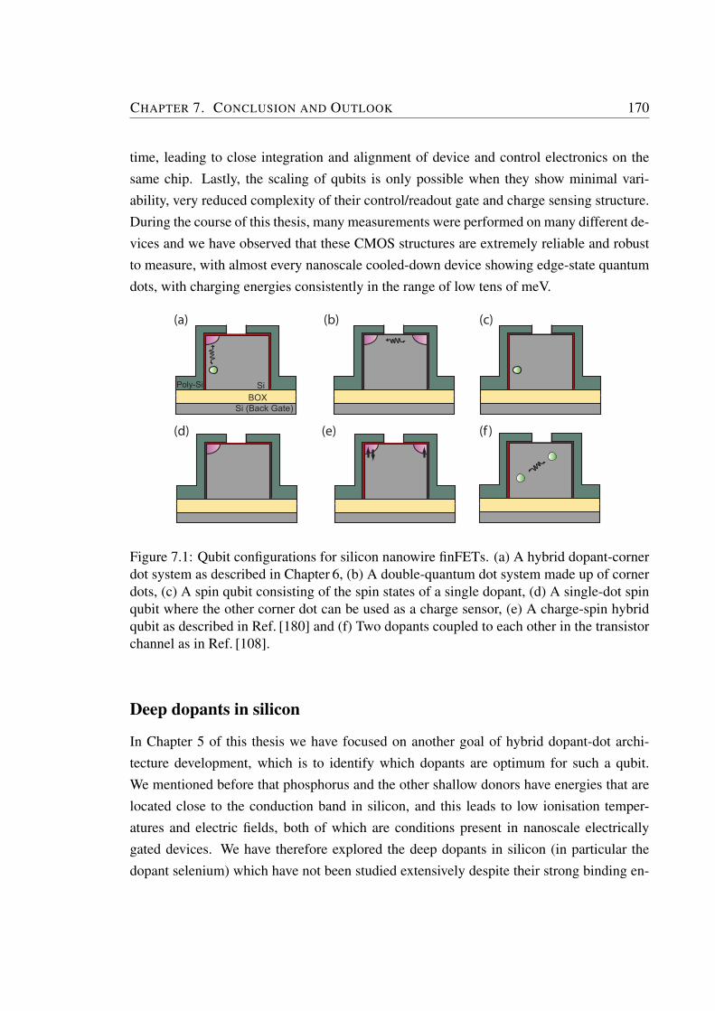
CHAPTER 7. CONCLUSION AND OUTLOOK 170
time, leading to close integration and alignment of device and control electronics on thesame chip. Lastly, the scaling of qubits is only possible when they show minimal vari-ability, very reduced complexity of their control/readout gate and charge sensing structure.During the course of this thesis, many measurements were performed on many different de-vices and we have observed that these CMOS structures are extremely reliable and robustto measure, with almost every nanoscale cooled-down device showing edge-state quantumdots, with charging energies consistently in the range of low tens of meV.
SiBOX
Si (Back Gate)
Poly-Si
(a) (b) (c)
(f )(e)(d)
Figure 7.1: Qubit configurations for silicon nanowire finFETs. (a) A hybrid dopant-cornerdot system as described in Chapter 6, (b) A double-quantum dot system made up of cornerdots, (c) A spin qubit consisting of the spin states of a single dopant, (d) A single-dot spinqubit where the other corner dot can be used as a charge sensor, (e) A charge-spin hybridqubit as described in Ref. [180] and (f) Two dopants coupled to each other in the transistorchannel as in Ref. [108].
Deep dopants in silicon
In Chapter 5 of this thesis we have focused on another goal of hybrid dopant-dot archi-tecture development, which is to identify which dopants are optimum for such a qubit.We mentioned before that phosphorus and the other shallow donors have energies that arelocated close to the conduction band in silicon, and this leads to low ionisation temper-atures and electric fields, both of which are conditions present in nanoscale electricallygated devices. We have therefore explored the deep dopants in silicon (in particular thedopant selenium) which have not been studied extensively despite their strong binding en-
CHAPTER 7. CONCLUSION AND OUTLOOK 171
ergies and very high ionization temperatures and fields. Selenium also possesses a stronghyperfine constant, leading it to be suitable for a dopant-dot hybrid qubit driven in the sin-glet triplet regime by the hyperfine gradient from the nuclear spin of the dopant. In thischapter we have explored this dopant using the tool of electrically detected magnetic res-onance (EDMR), and showed the first observation of spin-dependent transport through adeep dopant in selenium. An additional but equally strong motivation for this experiment isin the context of EDMR, where the chalcogens in silicon, by virtue of their deep and doubledonor nature, are expected to give rise to previously unknown EDMR mechanisms. Indeed,our study yields observations that cannot be adequately explained by EDMR mechanismscommonly used to describe spin dependent transport through shallow donors. We havetherefore presented a model of a new mechanism, that of spin dependent trapping basedon a difference in singlet-triplet capture rates; a mechanism that is not possible in shallowdonors since they lack bound triplet states. In future, the further exploration of EDMR inthe chalcogens as well as the integration of selenium dopants into devices are expected tobe exciting avenues for research.
Hybrid dopant-dot qubit
In Chapter 6 we put together the gate-based reflectometry technique and CMOS-SOIfoundry architecture described above to show a coupling between a single donor and anedge-state quantum dot in a nanowire transistor, and to establish that these two objectsbehave as a double quantum dot. We explored the coupled system as a charge qubit,measuring the relevant coherence and relaxation times, as well as the tunnel coupling.Finally, we presented a way to differentiate between the singlet and triplet spin states of thecoupled qubit and demonstrated Pauli spin blockade, a crucial first step towards a hybriddopant-dot spin qubit. We also showed progress towards coherent control, involving thedesign and fabrication of a stripline for controlling spin rotations. While this system isundoubtedly interesting for the purposes of quantum information, it also offers a novelplatform for looking at the unexplored physics of an asymmetrical double quantum dotmade up of an engineered artificial structure and a natural implanted atom, the latter havingthe additional degree of freedom of the nuclear spin.
Other advances developed during the course of this thesis have been the design of aflexible device platform in silicon MOS as a testbed for devices with more complicated gatestructures, as well as the development of a versatile and low-noise millielvin temperature
CHAPTER 7. CONCLUSION AND OUTLOOK 172
dilution fridge setup suitable for transport and gate based reflectometry measurements infew-electron quantum dots.
7.1 Outlook and future work
A few perspectives emerging out of the current work, and the direction in which furtherexperiments can be taken, are outlined below.
Electron spin resonance
Coherent control of the hybrid spin qubit is a logical next step after the demonstrationof spin blockade. Using the stripline design presented which is suitable for these siliconfoundry-made devices, experiments are possible that can use ESR to flip the elctron spinand hence lift the Pauli spin blockade shown in Chapter 6, recovering the signal at the ICT.Once this is established, pulsed ESR measurements can be performed to achieve coherentcontrol[58].
Charge noise
In our experiments, the measured dephasing rate is close to the tunnel splitting, limitingthe fidelity of coherent charge transfer to mediate spin information (the CTAP protocolmentioned in Section 1.4). Since in our system T1 T2, charge coherence is not limited byphonon coupling. Background charge noise in the gate voltages or charge fluctuations in thesample itself should be the main dephasing sources. The T2 measured for the quantum dotand dopant-dot systems in this thesis (measured in two different low-temperature systemsat different universities) are both similar, in the ∼200 ps range, and they are also similarto other measurements in these silicon nanowire transistors[108], leading us to believe thecharge noise identified is a feature of the device architecture or fabrication process. Thiscould be somewhat mitigated by removal of the nitride spacers in the device, known to beara large trapped charge density.
Tunability
Currently the device tunnel couplings presented in this thesis are not electrostatically tun-able, since there is only one gate which functions as a top gate. The tunnel coupling might
CHAPTER 7. CONCLUSION AND OUTLOOK 173
be tunable in a different architecture, for instance one with an extra top gate (such as in thedevice similar to ours, but with two facing-gates, used in Ref. [108]).
Spin blockade
The asymmetry in our demonstration of Pauli spin blockade for the dopant-dot hybrid qubit(Chapter 6) indicates a hybrid singlet-triplet spin qubit. In such a qubit, mixing between theS−T− states is generally induced by the nuclear spin bath’s magnetic field gradient. As wehave discussed previously, in this hybrid double dot the mixing should be dominated by thehyperfine interaction with the nuclear spin localized at the donor site. The time evolutionof such a singlet-triplet qubit should then be governed by the donor nuclear spin, enablingcontrolled rotation gates using NMR excitation. In the case of phosphorus, the S(1,1)-T0
coherent evolution at very low exchange coupling could be driven at ∼20MHz, with aneven higher frequency possible for bismuth or selenium.
Isotopic purification
The key factor behind the very long spin coherence times obtained in silicon is isotopic pu-rification. Using SOI wafers with a 28Si-rich device layer, grown by means of a chemicalvapor deposition (CVD) process, is possible in the foundry at CEA-Leti, where these de-vices were made. While obtaining isotopically purified silane required for the CVD processis a hurdle, such a development could result in an extremely scalable qubit with coherencetimes unparalleled in the solid state.
Nuclear spin memory
Long-term, the nuclear spin of the dopant that is essentially a bonus addition to our hy-brid spin quit is a useful resource for a long-lived quantum memory; it has been shownthrough ensemble measurements to have an (ionised) coherence time of 39 minutes atroom temperature[151]. Exploiting the hybrid qubit’s interdot exchange coupling wouldallow a SWAP operation between the quantum dot and the donor atom spin state. Eventu-ally this state could be stored in the donor nucleus using electro-nuclear double resonance(ENDOR) techniques. Finally, a potential further application could be the creation of spinbuses with quantum dot chains to mediate quantum information stored in these long-liveddonor qubits over long distances [22].
CHAPTER 7. CONCLUSION AND OUTLOOK 174
The results in this thesis represent some first steps towards a scalable hybrid dopant-dotarchitecture implemented in silicon and fabricated using industry compatible techniques. Ihave shown that our chosen silicon nanowire finFET architecture is a versatile platform forthe measurement of quantum dots using the technique of gate-based charge-sensing, whichallows close proximity to the quantum dot and accurate charge sensing without sacrificingease of fabrication. I have also shown that the nano-transistor channel is also a viable hostfor a coupled dopant-dot system behaving like a double quantum dot. With the observationof Pauli spin blockade and the promise of electron spin resonance in this hybrid quantumdot, the outlook on the coherent control of the spin system is bright. Further efforts tofabricate more controllable systems that retain versatility, for example devices with split-gates for tunable tunnel couplings and independent control of dots, promise to be veryfruitful in the future. In addition, the incorporation of more exotic dopants such as seleniuminto silicon devices might also be an intriguing avenue of research.
Appendix A
Fabrication Listings
Silicon MOS devicesTable A.1: Silicon MOS fabrication process flow
Step Step DetailsSiO2 Protective Layer
1 15 mins 1000C dry oxidation, target 20nm
Electron Beam Alignment Marks2 Dehydration, 210C, 20min3 HMDS prime4 Spin ZEP520A, 3370rpm, 180s5 Hot plate, 180C, 180s6 Exposure7 Develop ZED-N50, 2min, rinse HPLC-IPA,2min8 RIE Poly-Si etch (SF6:18, O2:13.5)
Continued on next page.
175
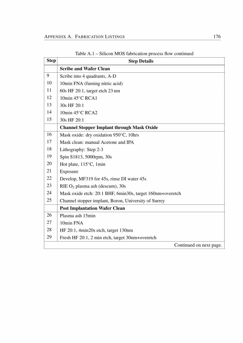
APPENDIX A. FABRICATION LISTINGS 176
Table A.1 – Silicon MOS fabrication process flow continuedStep Step Details
Scribe and Wafer Clean9 Scribe into 4 quadrants, A-D10 10min FNA (fuming nitric acid)11 60s HF 20:1, target etch 23 nm12 10min 45C RCA113 30s HF 20:114 10min 45C RCA215 30s HF 20:1
Channel Stopper Implant through Mask Oxide16 Mask oxide: dry oxidation 950C, 10hrs17 Mask clean: manual Acetone and IPA18 Lithography: Step 2-319 Spin S1813, 5000rpm, 30s20 Hot plate, 115C, 1min21 Exposure22 Develop, MF319 for 45s, rinse DI water 45s23 RIE O2 plasma ash (descum), 30s24 Mask oxide etch: 20:1 BHF, 6min30s, target 160nm+overetch25 Channel stopper implant, Boron, University of Surrey
Post Implantation Wafer Clean26 Plasma ash 15min27 10min FNA28 HF 20:1, 4min20s etch, target 130nm29 Fresh HF 20:1, 2 min etch, target 30nm+overetch
Continued on next page.
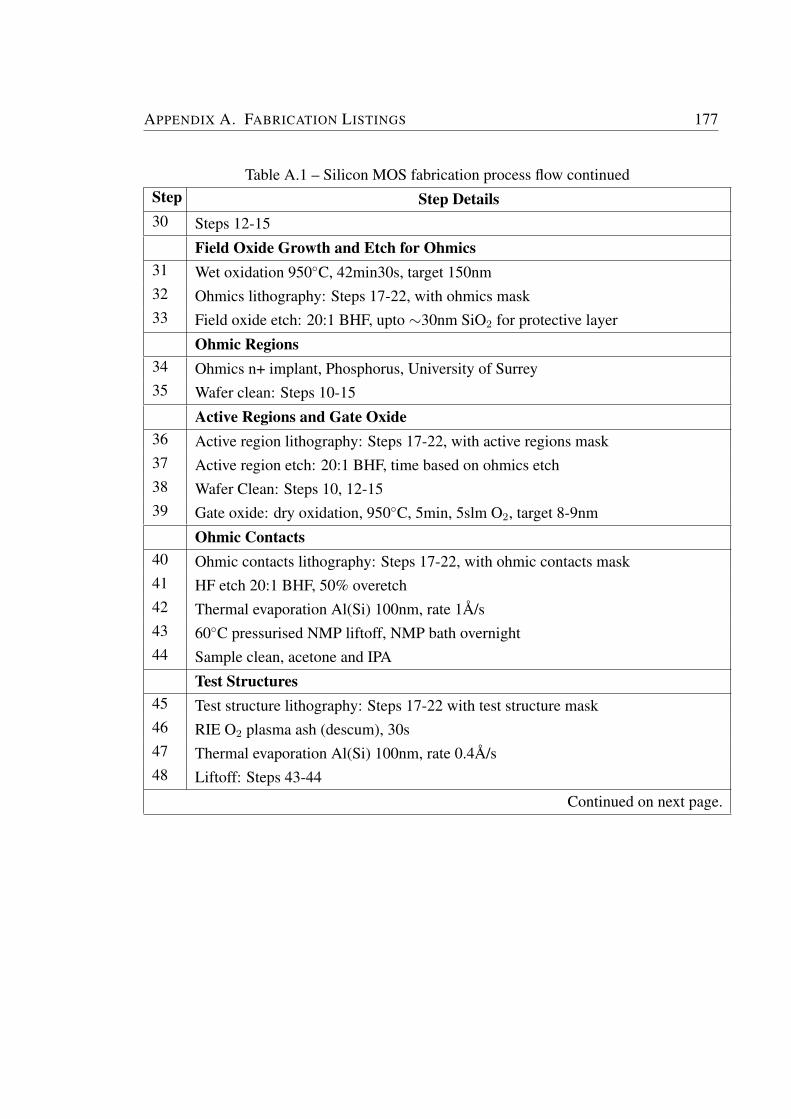
APPENDIX A. FABRICATION LISTINGS 177
Table A.1 – Silicon MOS fabrication process flow continuedStep Step Details30 Steps 12-15
Field Oxide Growth and Etch for Ohmics31 Wet oxidation 950C, 42min30s, target 150nm32 Ohmics lithography: Steps 17-22, with ohmics mask33 Field oxide etch: 20:1 BHF, upto ∼30nm SiO2 for protective layer
Ohmic Regions34 Ohmics n+ implant, Phosphorus, University of Surrey35 Wafer clean: Steps 10-15
Active Regions and Gate Oxide36 Active region lithography: Steps 17-22, with active regions mask37 Active region etch: 20:1 BHF, time based on ohmics etch38 Wafer Clean: Steps 10, 12-1539 Gate oxide: dry oxidation, 950C, 5min, 5slm O2, target 8-9nm
Ohmic Contacts40 Ohmic contacts lithography: Steps 17-22, with ohmic contacts mask41 HF etch 20:1 BHF, 50% overetch42 Thermal evaporation Al(Si) 100nm, rate 1A/s43 60C pressurised NMP liftoff, NMP bath overnight44 Sample clean, acetone and IPA
Test Structures45 Test structure lithography: Steps 17-22 with test structure mask46 RIE O2 plasma ash (descum), 30s47 Thermal evaporation Al(Si) 100nm, rate 0.4A/s48 Liftoff: Steps 43-44
Continued on next page.
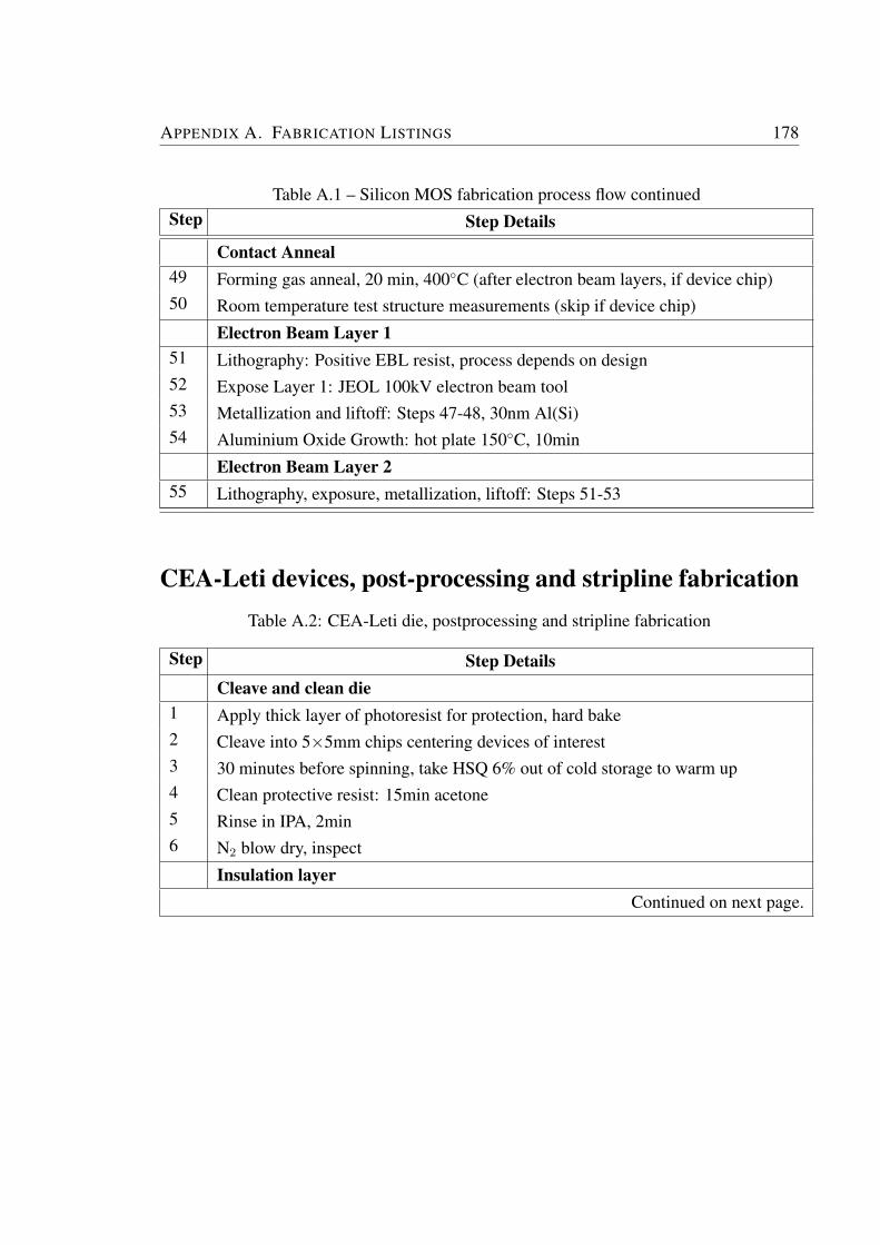
APPENDIX A. FABRICATION LISTINGS 178
Table A.1 – Silicon MOS fabrication process flow continuedStep Step Details
Contact Anneal49 Forming gas anneal, 20 min, 400C (after electron beam layers, if device chip)50 Room temperature test structure measurements (skip if device chip)
Electron Beam Layer 151 Lithography: Positive EBL resist, process depends on design52 Expose Layer 1: JEOL 100kV electron beam tool53 Metallization and liftoff: Steps 47-48, 30nm Al(Si)54 Aluminium Oxide Growth: hot plate 150C, 10min
Electron Beam Layer 255 Lithography, exposure, metallization, liftoff: Steps 51-53
CEA-Leti devices, post-processing and stripline fabricationTable A.2: CEA-Leti die, postprocessing and stripline fabrication
Step Step DetailsCleave and clean die
1 Apply thick layer of photoresist for protection, hard bake2 Cleave into 5×5mm chips centering devices of interest3 30 minutes before spinning, take HSQ 6% out of cold storage to warm up4 Clean protective resist: 15min acetone5 Rinse in IPA, 2min6 N2 blow dry, inspect
Insulation layerContinued on next page.
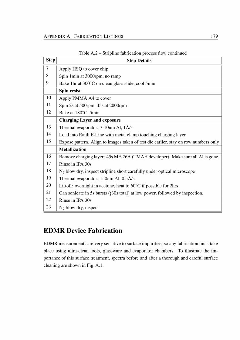
APPENDIX A. FABRICATION LISTINGS 179
Table A.2 – Stripline fabrication process flow continuedStep Step Details7 Apply HSQ to cover chip8 Spin 1min at 3000rpm, no ramp9 Bake 1hr at 300C on clean glass slide, cool 5min
Spin resist10 Apply PMMA A4 to cover11 Spin 2s at 500rpm, 45s at 2000rpm12 Bake at 180C, 5min
Charging Layer and exposure13 Thermal evaporator: 7-10nm Al, 1A/s14 Load into Raith E-Line with metal clamp touching charging layer15 Expose pattern. Align to images taken of test die earlier, stay on row numbers only
Metallization16 Remove charging layer: 45s MF-26A (TMAH developer). Make sure all Al is gone.17 Rinse in IPA 30s18 N2 blow dry, inspect stripline short carefully under optical microscope19 Thermal evaporator: 150nm Al, 0.5A/s20 Liftoff: overnight in acetone, heat to 60C if possible for 2hrs21 Can sonicate in 5s bursts (¡30s total) at low power, followed by inspection.22 Rinse in IPA 30s23 N2 blow dry, inspect
EDMR Device Fabrication
EDMR measurements are very sensitive to surface impurities, so any fabrication must takeplace using ultra-clean tools, glassware and evaporator chambers. To illustrate the im-portance of this surface treatment, spectra before and after a thorough and careful surfacecleaning are shown in Fig. A.1.
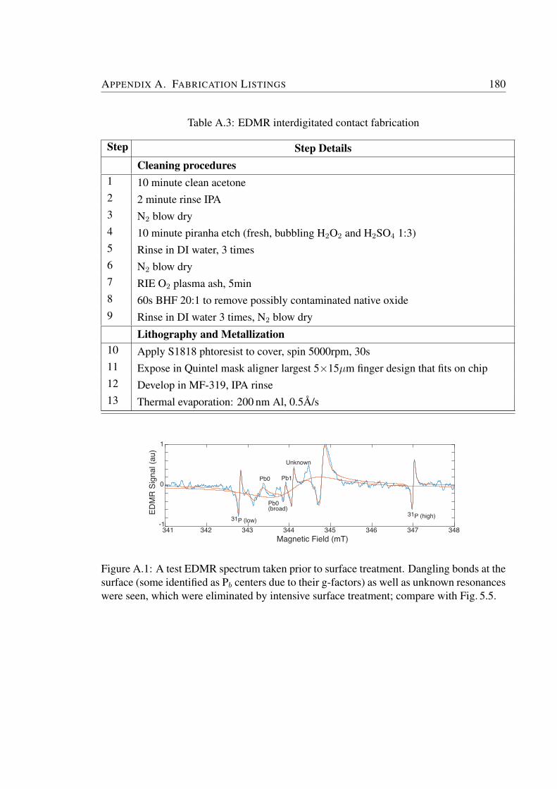
APPENDIX A. FABRICATION LISTINGS 180
Table A.3: EDMR interdigitated contact fabrication
Step Step DetailsCleaning procedures
1 10 minute clean acetone2 2 minute rinse IPA3 N2 blow dry4 10 minute piranha etch (fresh, bubbling H2O2 and H2SO4 1:3)5 Rinse in DI water, 3 times6 N2 blow dry7 RIE O2 plasma ash, 5min8 60s BHF 20:1 to remove possibly contaminated native oxide9 Rinse in DI water 3 times, N2 blow dry
Lithography and Metallization10 Apply S1818 phtoresist to cover, spin 5000rpm, 30s11 Expose in Quintel mask aligner largest 5×15µm finger design that fits on chip12 Develop in MF-319, IPA rinse13 Thermal evaporation: 200 nm Al, 0.5A/s
Magnetic Field (mT)341 342 343 344 345 346 347 348
EDM
R S
igna
l (au
)
-1
0
1
Pb0(broad)
31P (high)31P (low)
Pb0 Pb1
Unknown
Figure A.1: A test EDMR spectrum taken prior to surface treatment. Dangling bonds at thesurface (some identified as Pb centers due to their g-factors) as well as unknown resonanceswere seen, which were eliminated by intensive surface treatment; compare with Fig. 5.5.

Appendix B
Measurement Notes
Measurement of foundry-fabricated silicon devices
We have explained the basics of the gate-based reflectometry measurements used in thisthesis in Chapter 3. In this section, we describe sequentially how to efficiently use the setupdescribed to measure a double quantum dot and attain a suitable level of charge sensitivity.We also present some considerations for improvement.
Identification of samples
Foundry-fabricated devices are typically far more robust and reliable across a large waferthan those made in university research cleanrooms. However, some considerations are:
• Avoid dies from the very edge of a wafer; these tend to have the worst of the typicalvariations across wafers, even foundry-fabricated ones.
• Avoid channels that are very small, if looking for double quantum dot systems. Thesedots tend to be extremely well coupled to each other, and to have very similar leverarms to the top gate, leading to an almost invisible quantum capacitance signal at theinterdot charge transition. However, with a tunable coupling, or more than one gate,these could be useful devices to measure. Samples in the range of 40 nm to 60 nmare typically interesting.
• If a probe able to work at 4 K that is equipped with an RF setup is available for quicktesting, this is invaluable for identifying a sample with a good dopant-dot or doublequantum dot system before cooling down in a dilution refrigerator.
181
APPENDIX B. MEASUREMENT NOTES 182
Wirebonding
Wirebonding is a little trickier for SOI devices, especially those with very small bond padsmade for automatic and accurate wirebonding in large foundries. These typically have verysmall gaps between devices, and the bond pads themselves can be effectively even smallerif a stripline is added that partially extends over them. A few tricks are:
• When bonding, bond to the source and drain of the device first, and then the gate(s).
• A small 15µm×15µm bonder wedge, with 15µm diameter Al bond wire, has beenfound to work much better for these devices, increasing the post-bonding yield dra-matically.
• Make sure to ground the pins carefully, together and to ground, when transferring tothe dilution fridge, and check for shorts between the leads/gates and the stripline, ifusing.
Testing of samples
These samples can be tested at room temperature, which is an immense bonus, since theydo not require a full fridge cooldown cycle before one can find out that whether the deviceis working or not. A simple and quick procedure to follow for this would be:
• Load the sample with the source connected to a small bias (∼1 mV) and the drainconnected to your current amplifier and digital multimeter of choice (this setup isuseful for later DC measurements as well) and connect a voltage source to the gate.
• Apply a voltage, in 0.1 mV increments, to the gate. The source-drain current shouldthen show turn-on around 0.2-0.6 V typically. Don’t exceed 1 V on the gate since thiscan blow the sample.
• If the device turns on, it will most likely show double quantum dot behaviour at lowtemperature and is worth cooling down.
• If the device is doped and has a lower threshold than others of the same channel size,this has been found to indicate a higher chance of finding a dopant in the channel.
• For making observations of the above sort, it is highly advisable to keep a log of chan-nel size, turn-on voltage, low-temperature behaviour, and other observations aboutmeasured devices.
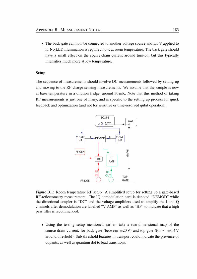
APPENDIX B. MEASUREMENT NOTES 183
• The back gate can now be connected to another voltage source and ±5 V applied toit. No LED illumination is required now, at room temperature. The back gate shouldhave a small effect on the source-drain current around turn-on, but this typicallyintensifies much more at low temperature.
Setup
The sequence of measurements should involve DC measurements followed by setting upand moving to the RF charge sensing measurements. We assume that the sample is nowat base temperature in a dilution fridge, around 30 mK. Note that this method of takingRF measurements is just one of many, and is specific to the setting up process for quickfeedback and optimization (and not for sensitive or time-resolved qubit operation).
AWGSCOPE
RT AMP
V-AMPHP
V-AMPHP
DEMODI Q
I Q RAMP
RAM
P
TOP GATE
RF OUT
RFIN
RF GEN
DC
FRIDGE
Figure B.1: Room temperature RF setup. A simplified setup for setting up a gate-basedRF-reflectometry measurement. The IQ demodulation card is denoted “DEMOD” whilethe directional coupler is “DC” and the voltage amplifiers used to amplify the I and Qchannels after demodulation are labelled “V AMP” as well as “HP” to indicate that a highpass filter is recommended.
• Using the testing setup mentioned earlier, take a two-dimensional map of thesource-drain current, for back-gate (between ±20 V) and top-gate (for ∼ ±0.4 Varound threshold). Sub-threshold features in transport could indicate the presence ofdopants, as well as quantum dot to lead transitions.
APPENDIX B. MEASUREMENT NOTES 184
• For changing the back gate, an LED needs to be turned on. This can be flashed for2 seconds, or kept on if just tuning up the device (this has been found to be disruptivefor some devices, but not for others). Remember that the biasing of this LED will bedifferent from that at room temperature. When the LED is correctly on and working,the fridge should heat up by a few millikelvin.
• Connect the resonator lines (connected via a bias tee to the top gate of the device) to aVector Network Analyser. You should see a resonance around the resonant frequency(350 MHz for our setup), in transmission mode (S21). Record the resonance whilesweeping the back gate (with the blue LED biased on), since the resonance dependson the back gate position. The resonator driving frequency will need to be set to thecorrect value based on where in back gate space we are measuring.
• Set up the instruments as shown in Fig. B.1 and apply a low power of 5 dBm at theresonance frequency (measured on the VNA previously), for the back gate voltageyou are at. Do not connect to the IQ demodulator card (or mixer) yet since these canbe damaged at too high a power, or to the fridge ports.
• Using a handheld power sensor (Rohde and Schwarz make a good one), check thepower going into the fridge reflectometry port, and after calculating the power reach-ing the sample (based on the attenuation inside the fridge), connect to the fridge port.Then including the amplifier into your calculations, check the power coming out ofthe fridge. If all is well, check the power that will go into the IQ demodulator cardor mixer; this should be within the optimum range specified by the manufacturer.Finally, connect everything according to Fig. B.1.
• Change the gate voltages so that you are at the first interesting feature in gate space,as seen on the DC measurement. If changing the back gate, make sure to change theresonator drive frequency you are using accordingly.
• Using the arbitrary waveform generator, apply a ramp to the top gate (a slow rampof 33Hz, driving around 100 mV around the feature identified in DC transport, is agood starting value; the best frequency is a matter of trial and error). Trigger anoscilloscope with this ramp and connect the amplified IQ signals coming from thevoltage amplifiers in Fig. B.1 to two oscilloscope channels, using AC coupling.
APPENDIX B. MEASUREMENT NOTES 185
• If you’ve done the steps before correctly and everything is well, you should nowimmediately see clear resonances on the oscilloscope. Factors that can be tuned arethe resonant frequency, the resonator drive, and the addition of room temperatureattenuation. A good starting measurement is a gate stability diagram.
Other dopant-dot devices measured and results
In this section we present two other doped foundry-fabricated devices in which dopant sig-natures were seen. Fig. B.1(a) shows a device measured by our collaborators at the Univer-sity of New South Wales, Australia1. This device was doped with phosphorus donors, buthad a wider and larger channel (240 nm×100 nm×10 nm). A tank circuit with a resonantfrequency of 671 MHz was connected to the top gate, a small AC excitation was appliedto the drain at frequency of 1.1 kHz and the amplitude of the resonant side band (671.0011MHz) was measured as a function of top gate and back gate using a spectrum analyzer. Thepresence of numerous charge transitions in the figure can be attributed to the larger numberof dopants in the channel compared to the device presented in Chapter 6. The left panel ofFig. B.1(a) shows a close-up of the stability diagram where a donor-based interdot chargetransition is visible, similar to our observations. Fig. B.1(b) shows a doped device with asmaller channel (30 nm×40 nm), measured by me at the Center for Quantum Devices, Uni-versity of Copenhagen. In this device as well, signature subthreshold resonances indicativeof dopants, coupled much more to the back gate, were seen, though fewer in number dueto the much smaller channel. This device harboured dopants which were not sufficientlytunnel coupled to the corner dot whose transitions it intersected with; this kind of systemprovides a major motivation for the movement to devices with the top gate split into twoas mentioned before, since then the tunnel coupling could be controlled for the establish-ment of a dopant-dot qubit using this kind of transition. Since many doped devices showdopant transitions, but coupled to various extents with the corner quantum, the tuning ofthis coupling could be of great help to form a consistent architecture of dopant-dot qubits.
These additional measurements indicate the flexibility of these devices and the range ofmeasurement setups in various laboratories in which they have been found to yield mea-surable corner quantum dots, as well as donor-dot couplings.
1The data shown was taken by Dr. Takeshi Kobayashi.
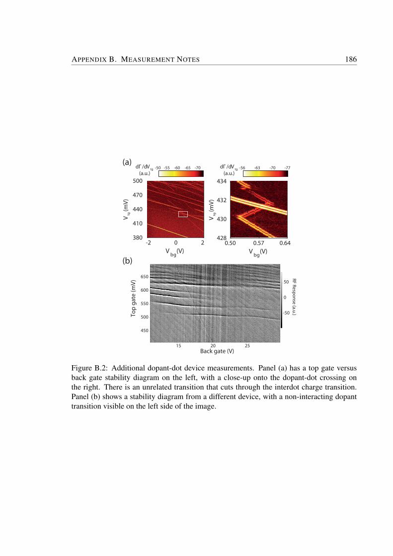
APPENDIX B. MEASUREMENT NOTES 186
Vbg
(V)-2 0 2
380
410
440
470
500
Vtg
(mV)
Vbg
(V)0.50 0.57 0.64
428
430
432
434
Vtg
(mV)
-70-65-60-55-50dΓ /dV tg (a.u.)
-77-70-63-56dΓ /dV tg (a.u.)
Dopants
Back gate (V)
Top
gate
(mV)
252015
-50
0
50650
600
550
500
450
RF Response (a.u.)
(a)
(b)
Figure B.2: Additional dopant-dot device measurements. Panel (a) has a top gate versusback gate stability diagram on the left, with a close-up onto the dopant-dot crossing onthe right. There is an unrelated transition that cuts through the interdot charge transition.Panel (b) shows a stability diagram from a different device, with a non-interacting dopanttransition visible on the left side of the image.
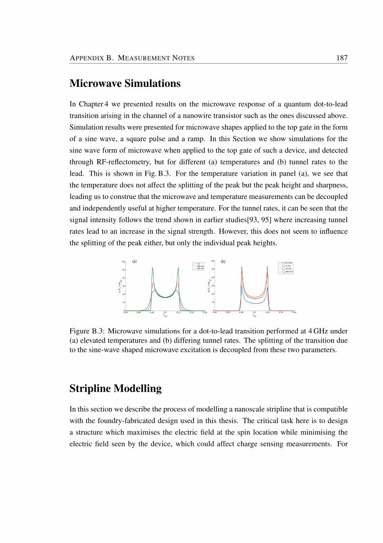
APPENDIX B. MEASUREMENT NOTES 187
Microwave Simulations
In Chapter 4 we presented results on the microwave response of a quantum dot-to-leadtransition arising in the channel of a nanowire transistor such as the ones discussed above.Simulation results were presented for microwave shapes applied to the top gate in the formof a sine wave, a square pulse and a ramp. In this Section we show simulations for thesine wave form of microwave when applied to the top gate of such a device, and detectedthrough RF-reflectometry, but for different (a) temperatures and (b) tunnel rates to thelead. This is shown in Fig. B.3. For the temperature variation in panel (a), we see thatthe temperature does not affect the splitting of the peak but the peak height and sharpness,leading us to construe that the microwave and temperature measurements can be decoupledand independently useful at higher temperature. For the tunnel rates, it can be seen that thesignal intensity follows the trend shown in earlier studies[93, 95] where increasing tunnelrates lead to an increase in the signal strength. However, this does not seem to influencethe splitting of the peak either, but only the individual peak heights.
ng0
0.44 0.46 0.48 0.5 0.52 0.54 0.56
d<P 1>/
dng0
0
10
20
30
40
50
601 K500 mK200 mK
(a) (b)
Figure B.3: Microwave simulations for a dot-to-lead transition performed at 4 GHz under(a) elevated temperatures and (b) differing tunnel rates. The splitting of the transition dueto the sine-wave shaped microwave excitation is decoupled from these two parameters.
Stripline Modelling
In this section we describe the process of modelling a nanoscale stripline that is compatiblewith the foundry-fabricated design used in this thesis. The critical task here is to designa structure which maximises the electric field at the spin location while minimising theelectric field seen by the device, which could affect charge sensing measurements. For
APPENDIX B. MEASUREMENT NOTES 188
this purpose, we follow previous work by J. P. Dehollain et al. [179], where four differentdesigns of nanoscale transmission lines were compared2.
Choice of Design: The two main contenders were (a) the on-PCB coplanar waveguidewith an on-chip coplanar waveguide terminated by a short, and (b) an on-chip CPW-CPSbalun (for balancing the transition) design developed by the team behind the work. Whileboth these designs had similar transmission characteristics with minimal stray reflections,the latter design had the advantage that the current (and hence the field strength) was nothalved at the spin location. For our purposes, and for compatibility with the foundry-fabricated devices described above (where the dies have devices spaced very closely to-gether), we chose the former design due to space constraints. In addition the design has thewidest range of operating frequencies and the lowest insertion loss, since there are no modeconversions[179]. This type of design was used by Fuchs et al. [112] to drive the ESR of anitrogen-vacancy centre in diamond.
Impedance Matching: The CPW will have to be impedance-matched to the coaxialcable that delivers the microwave. For 50 Ω matching, the characteristic impedance ofplanar transmission lines needs to be taken into account; this is typically a function of thewidth and thickness of the metal strips, the gap between coplanar strips and the thicknessof the dielectric. These parameters were tweaked and modelled in TX-Line, a transmissionline calculator from Applied Wave Research, including the PCB characteristics (Rogers4003C laminate).
Modelling: The software used to model the CPW was CST Microwave Studio, a full-3D microwave engineering software that can be used to model the electric and magneticfields from the stripline as well. Using this software, we were able to model the wholestructure, including the chip and the PCB, as well as the bond wires and the SMA connectordelivering the input power, as shown in Chapter 6.
Solver and Meshing: Within CST, the finite integration method (FIM) in the frequencydomain was used (repeated to obtain broadband results), with tetrahedral meshing. Subdi-vided meshes were used to increase the mesh detail near the crucial nanoscale short of theCPW, while the mesh was left less detailed elsewhere.
Probes and Fields: Electric and magnetic field probes were placed in a grid aroundthe stripline to determine the best position to align with the device. Since our striplineis located above the sample (as is the case in Koppens et al. [58], the first demonstration
2Improvements to my initial design and meshing were made by Simon Schaal.
APPENDIX B. MEASUREMENT NOTES 189
of single-spin ESR in a quantum dot), there is more flexibility compared with Ref. [179]where the device geometry only left a particular coplanar position for the CPS.
Transmission and Fields: Our results and field distributions are shown in Fig. B.4, (weassume 1 mW at the input port, taking into account the attenuation in our dilution fridge).The transmission of the design is excellent, with the simulations showing that the fully-CPW structure shows near-ideal behaviour, with S11 ≈0 dB from 0 to 40 GHz, as foundin Ref. [179] (where it was also found that this design radiated the smallest electric fieldat the spin location). Field strengths for our design are shown in Fig. B.4 as well. We seethat the field strength decreases strongly with distance from the central pin, which confirmsthe importance of lowering the level of encapsulation of these foundry-fabricated devices.However, with a field intensity in the high µT range, we hope to be able to observe cw-ESRfrom our dopant-dot devices.
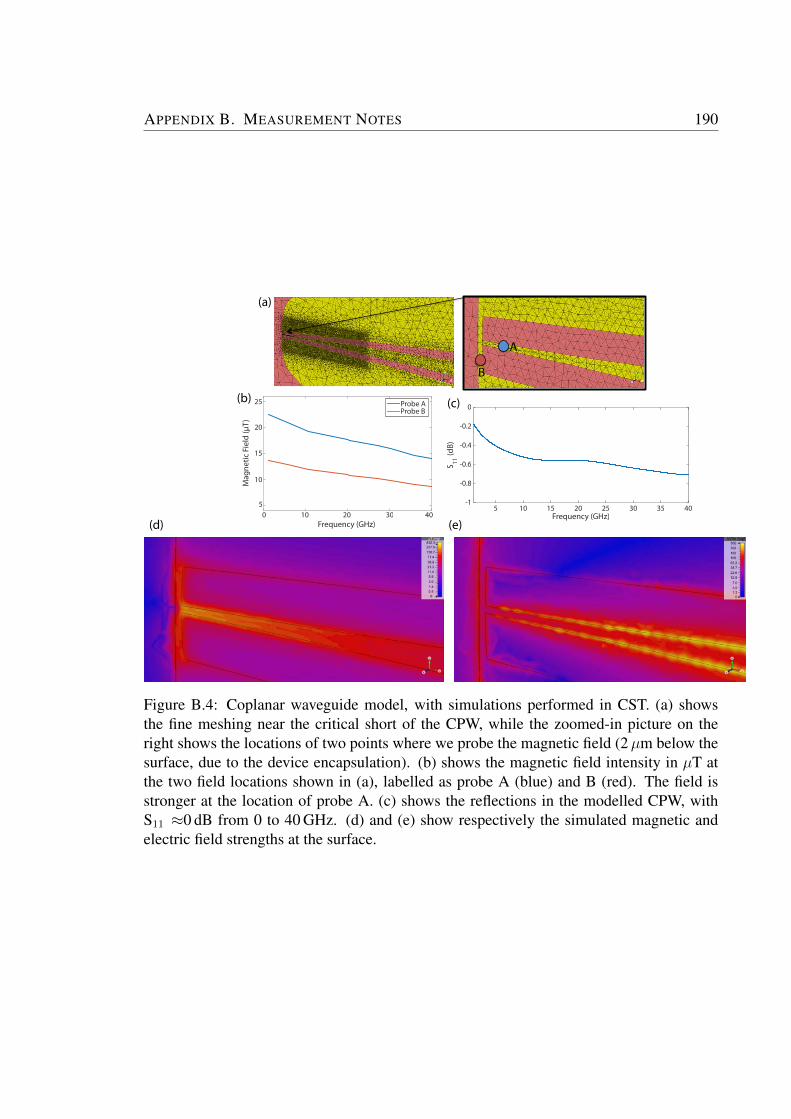
APPENDIX B. MEASUREMENT NOTES 190
Frequency (GHz)5 10 15 20 25 30 35 40
S 11 (d
B)
-1
-0.8
-0.6
-0.4
-0.2
0
0 10 20 30 405
10
15
20
25 Probe AProbe B
Frequency (GHz)
Mag
netic
Fie
ld (μ
T)
A
B
(a)
(b) (c)
(d) (e)
Figure B.4: Coplanar waveguide model, with simulations performed in CST. (a) showsthe fine meshing near the critical short of the CPW, while the zoomed-in picture on theright shows the locations of two points where we probe the magnetic field (2µm below thesurface, due to the device encapsulation). (b) shows the magnetic field intensity in µT atthe two field locations shown in (a), labelled as probe A (blue) and B (red). The field isstronger at the location of probe A. (c) shows the reflections in the modelled CPW, withS11 ≈0 dB from 0 to 40 GHz. (d) and (e) show respectively the simulated magnetic andelectric field strengths at the surface.
Bibliography
[1] International technology roadmap for semiconductors, http://www.itrs.net (2009).
[2] P. Shor, Algorithms for quantum computation: discrete logarithms and factoring,Proceedings, 35th annual symposium on foundations of computer science (1994).
[3] R. P. Feynman, Simulating physics with computers, International Journal of Theo-retical Physics 21, 467 (1982).
[4] D. P. DiVincenzo, The physical implementation of quantum computation, Fortschr.Phys. 48, 711 (2000).
[5] B. Kane, A silicon-based nuclear spin quantum computer, Nature 393, 133 (1998).
[6] A. Morello, J. J. Pla, F. A. Zwanenburg, K. W. Chan, and K. Y. Tan, Single-shotreadout of an electron spin in silicon, Nature 467, 687 (2010).
[7] J. J. Pla, K. Y. Tan, J. P. Dehollain, W. H. Lim, J. J. L. Morton, D. N. Jamieson, A. S.Dzurak, and A. Morello, A single-atom electron spin qubit in silicon, Nature 489,541 (2012).
[8] J. J. Pla, K. Y. Tan, J. P. Dehollain, W. H. Lim, J. J. L. Morton, F. A. Zwanenburg,D. N. Jamieson, A. S. Dzurak, and A. Morello, High-fidelity readout and control ofa nuclear spin qubit in silicon, Nature 496, 334 (2013).
[9] J. T. Muhonen, J. P. Dehollain, A. Laucht, F. E. Hudson, R. Kalra, T. Sekiguchi,K. Itoh, D. N. Jamieson, J. C. McCallum, A. S. Dzurak, et al., Storing quantuminformation for 30 seconds in a nanoelectronic device, Nature Nanotechnology 9,986 (2013).
[10] J. van Donkelaar, C. Yang, A. Alves, J. McCallum, C. Hougaard, B. Johnson, F. Hud-son, A. S. Dzurak, A. Morello, D. Spemann, et al., Single atom devices by ion im-plantation, Journal of Physics: Condensed Matter 27, 15 (2015).
[11] M. Fuechsle, J. Miwa, S. Mahapatra, H. Ryu, S. Lee, O. Warschkow, L. C. L. Hol-lenberg, G. Klimeck, and M. Y. Simmons, A single-atom transistor, Nature Nan-otechnology 7, 242 (2012).
191
BIBLIOGRAPHY 192
[12] F. Bradbury, A. Tyryshkin, G. Sabouret, J. Bokor, T. Schenkel, and S. A. Lyon, Starktuning of donor electron spins in silicon, Physical Review Letters 97, 176404 (2006).
[13] G. Wolfowicz, M. Urdampilleta, M. L. W. Thewalt, H. Riemann, N. V. Abrosimov,P. Becker, H.-J. Pohl, and J. J. L. Morton, Conditional control of donor nuclear spinsin silicon using Stark shifts, Physical Review Letters 113, 157601 (2014).
[14] A. Laucht, J. T. Muhonen, F. A. Mohiyaddin, R. Kalra, J. P. Dehollain, S. Freer,F. E. Hudson, M. Veldhorst, R. Rahman, G. Klimeck, et al., Electrically controllingsingle-spin qubits in a continuous microwave field, Science Advances 1, 1500022(2015).
[15] B. Koiller, X. Hu, and S. D. Sarma, Exchange in silicon-based quantum computerarchitecture, Physical Review Letters 88, 027903 (2002).
[16] J. J. L. Morton, A. M. Tyryshkin, R. M. Brown, S. Shankar, B. W. Lovett, A. Ar-davan, T. Schenkel, E. E. Haller, J. W. Ager, and S. A. Lyon, Solid state quantummemory using the 31P nuclear spin, Nature 455, 1085 (2008).
[17] M. Veldorst, J. Hwang, C. Yang, A. Leenstra, B. de Ronde, J. Dehollain, J. Muhonen,F. Hudson, K. Itoh, A. Morello, et al., An addressable quantum dot qubit with fault-tolerant control fidelity, Nature Nanotechnology 9, 981 (2014).
[18] M. Veldorst, C. Yang, J. Hwang, W. Huang, J. Dehollain, J. Muhonen, S. Simmons,A. Laucht, F. Hudson, K. Itoh, et al., A two qubit logic gate in silicon, Nature 526,410 (2015).
[19] T. Schenkel, C. C. Lo, C. D. Weis, J. Bokor, A. M. Tyryshkin, and S. A. Lyon, inSingle-Atom Nanoelectronics, edited by E. Prati and T. Shinada (Taylor and FrancisGroup, 2013), p. 255.
[20] D. Loss and D. P. DiVincenzo, Quantum computation with quantum dots, PhysicalReview A 57, 120 (1998).
[21] D. M. Zajac, T. M. Hazard, X. Mi, E. Nielsen, and J. R. Petta, Scalable gate archi-tecture for a one-dimensional array of semiconductor spin qubits, Phys. Rev. Applied6, 054013 (2016).
[22] M. Friesen, A. Biswas, X. Hu, and D. Lidar, Efficient multiqubit entanglement via aspin bus, Physical Review Letters 98, 1 (2007).
[23] K. D. Petersson, C. G. Smith, D. Anderson, P. Atkinson, G. A. C. Jones, and D. A.Ritchie, Charge and spin state readout of a double quantum dot coupled to a res-onator., Nano letters 10, 2789 (2010).
BIBLIOGRAPHY 193
[24] A. D. Greentree, J. H. Cole, A. R. Hamilton, and L. C. L. Hollenberg, Coherentelectronic transfer in quantum dot systems using adiabatic passage, Physical ReviewB 70, 235317 (2004).
[25] R. Rahman, R. P. Muller, J. E. Levy, M. S. Carroll, G. Klimeck, A. D. Greentree, andL. C. L. Hollenberg, Coherent electron transport by adiabatic passage in an imperfectdonor chain, Physical Review B 82, 1 (2010).
[26] T. A. Baart, M. Shafiei, T. Fujita, C. Reichl, W. Wegscheider, and L. M. K. Vander-sypen, Single-spin ccd, Nature Nanotechnology 11, 330 (2016).
[27] M. F. Gonzalez-Zalba, D. Heiss, and A. J. Ferguson, A hybrid double-dot in silicon,New Journal of Physics 14, 023050 (2012).
[28] H. Sellier, G. P. Lansbergen, J. Caro, and S. Rogge, Transport spectroscopy of a sin-gle dopant in a gated silicon nanowire, Physical Review Letters 97, 206805 (2006).
[29] M. Urdampilleta, A. Chatterjee, C. C. Lo, T. Kobayashi, J. Mansir, S. Barraud, A. C.Betz, S. Rogge, M. F. Gonzalez-Zalba, and J. J. Morton, Charge dynamics and spinblockade in a hybrid double quantum dot in silicon, Physical Review X 5, 031024(2015).
[30] P. Harvey-Collard, N. T. Jacobson, M. Rudolph, J. Dominguez, G. A. Ten Eyck,J. R. Wendt, T. Pluym, J. K. Gamble, M. P. Lilly, M. Pioro-Ladriere, et al., Nuclear-driven electron spin rotations in a single donor coupled to a silicon quantum dot,arXiv:1512.01606v1 (2015).
[31] R. Hanson, L. P. Kouwenhoven, J. R. Petta, S. Tarucha, and L. M. K. Vandersypen,Spins in few-electron quantum dots, Reviews of Modern Physics 79, 1217 (2007).
[32] L. Hofstetter, S. Csonka, J. Nygard, and C. Schonenberger, Cooper pair splitter real-ized in a two-quantum-dot Y-junction, Nature 461, 960 (2009).
[33] F. Pei, E. A. Laird, G. A. Steele, and L. P. Kouwenhoven, Valley-spin blockade andspin resonance in carbon nanotubes, Nature Nanotechnology 7, 630 (2012).
[34] J. Baugh, Y. Kitamura, K. Ono, and S. Tarucha, Large nuclear Overhauser fieldsdetected in vertically coupled double quantum dots, Physical Review Letters 99,096804 (2007).
[35] D. Schroer, S. Ludwig, J. P. Kotthaus, K. Eberl, and W. Wegscheider, ResearchReports: Quantum dots as quantum bits (L. M. Universitat Meunchen, Meunchen,2004).
[36] W. G. Van der Wiel, S. de Franceschi, J. M. Elzerman, T. Fujisawa, S. Tarucha, andL. P. Kouwenhoven, Electron transport through double quantum dots, Reviews ofModern Physics 75, 1 (2002).
BIBLIOGRAPHY 194
[37] L. P. Kouwenhoven, D. G. Austing, and S. Tarucha, Few-electron quantum dots,Reports on Progress in Physics 64, 701 (2001).
[38] T. Fujisawa, T. Hayashi, and S. Sasaki, Time-dependent single-electron transportthrough quantum dots, Reports on Progress in Physics 69, 759 (2006).
[39] T. Hayashi, T. Fujisawa, H. D. Cheong, Y. H. Jeong, and Y. Hirayama, Coherentmanipulation of electronic states in a double quantum dot, Physical Review Letters91, 226804 (2003).
[40] T. H. Oosterkamp, T. Fujisawa, and W. G. Van der Wiel, Microwave spectroscopyof a quantum-dot molecule, Nature 395, 873 (1998).
[41] J. R. Petta, A. C. Johnson, C. M. Marcus, M. P. Hanson, and A. C. Gossard, Ma-nipulation of a single charge in a double quantum dot, Physical Review Letters 93,186802 (2004).
[42] K. W. Lehnert, K. Bladh, L. F. Spietz, D. Gunnarsson, D. I. Schuster, P. Delsing,and R. J. Schoelkopf, Measurement of the excited-state lifetime of a microelectroniccircuit, Physical Review Letters 90, 027002 (2003).
[43] S. N. Shevchenko, S. Ashab, and F. Nori, Landau–Zener–Stuckelberg interferome-try, Physics Reports 492, 1 (2010).
[44] B. Damski and W. H. Zurek, Adiabatic-impulse approximation for avoided levelcrossings: from phase-transition dynamics to Landau–Zener evolutions and backagain, Physical Review A 73, 063405 (2006).
[45] J. Stehlik, M. Z. Maialle, M. H. Degani, and J. R. Petta, Role of multilevel Landau–Zener interference in extreme harmonic generation, Phys. Rev. B 94, 075307 (2016).
[46] M. F. Gonzalez-Zalba, S. N. Shevchenko, S. Barraud, J. R. Johansson, A. J. Fergu-son, F. Nori, and A. C. Betz, Gate-sensing coherent charge oscillations in a siliconfield-effect transistor, Nano Letters 16, 1614 (2016).
[47] L. D. Landau and E. M. Lifshitz, Quantum Mechanics: Non-Relativistic Theory(Pergamon Press, Oxford, 1977).
[48] L. D. Landau, A theory of energy transfer on collisions, Physikalische Zeitschriftder Sowjetunion 1, 88 (1932).
[49] E. C. G. Stuckelberg, Theory of inelastic collisions between atoms, Helvetica Phys-ica Acta 5, 369 (1932).
[50] J. R. Petta, H. Lu, and A. C. Gossard, A coherent beam splitter for electronic spinstates, Science 327, 669 (2010).
BIBLIOGRAPHY 195
[51] K. D. Petersson, J. R. Petta, H. Lu, and A. C. Gossard, Quantum coherence in a one-electron semiconductor charge qubit, Physical Review Letters 105, 246804 (2010).
[52] K. Wang, Few-electron Qubits in Silicon Quantum Electronic Devices (PhD Thesis:Princeton University, Princeton, 2014).
[53] Y. Nakamura, Y. A. Pashkin, and J. S. Tsai, Coherent control of macroscopic quan-tum states in a single-Cooper-pair box, Nature 398, 786 (1999).
[54] D. Rugar, R. Budakian, H. J. Mamin, and B. W. Chui, Single spin detection bymagnetic resonance force microscopy, Nature 430, 329 (2004).
[55] M. S. Grinolds, P. Maletinsky, S. Hong, M. D. Lukin, R. L. Walsworth, and A. Ya-coby, Quantum control of proximal spins using nanoscale magnetic resonance imag-ing, Nature Physics 7, 687 (2011).
[56] J. M. Elzerman, R. Hanson, L. H. Willems van Beveren, B. Witkamp, L. M. K.Vandersypen, and L. P. Kouwenhoven, Single-shot read-out of an individual electronspin in a quantum dot, Nature 430, 431 (2004).
[57] A. C. Johnson, J. R. Petta, C. M. Marcus, M. P. Hanson, and A. C. Gossard, Singlet-triplet spin blockade and charge sensing in a few-electron double quantum dot, Phys-ical Review B 72, 165308 (2005).
[58] F. H. L. Koppens, C. Buizert, K. J. Tielrooij, I. T. Vink, K. C. Nowack, T. Meunier,L. P. Kouwenhoven, and L. M. K. Vandersypen, Driven coherent oscillations of asingle electron spin in a quantum dot, Nature 442, 766 (2006).
[59] K. C. Nowack, F. H. L. Koppens, Y. V. Nazarov, and L. M. K. Vandersypen, Coherentcontrol of a single electron spin with electric fields, Science 318, 1430 (2007).
[60] M. Pioro-Ladriere, T. Obata, Y. Tokura, Y. S. Shin, and T. Kubo, Electrically drivensingle-electron spin resonance in a slanting Zeeman field, Nature Physics 4, 776(2008).
[61] E. Kawakami, P. Scarlino, D. R. Ward, F. R. Braakman, D. E. Savage, M. G. La-gally, M. Friesen, S. N. Coppersmith, M. A. Eriksson, and L. M. K. Vandersypen,Electrical control of a long-lived spin qubit in a Si/SiGe quantum dot, Nature Nan-otechnology 9, 666 (2014).
[62] E. A. Laird, C. Barthel, E. I. Rashba, C. M. Marcus, M. P. Hanson, and A. C. Gos-sard, Hyperfine-mediated gate-driven electron spin resonance, Physical Review Let-ters 99, 246601 (2007).
BIBLIOGRAPHY 196
[63] T. Meunier, I. T. Vink, L. H. W. van Beveren, K. J. Tielrooij, R. Hanson, F. H. L.Koppens, H. P. Tranitz, W. Wegscheider, L. P. Kouwenhoven, and L. M. K. Vander-sypen, Experimental signature of phonon-mediated spin relaxation in a two-electronquantum dot, Physical Review Letters 98, 126601 (2007).
[64] J. Levy, Universal quantum computation with spin-1/2 Pairs and Heisenberg ex-change, Physical Review Letters 89, 147902 (2002).
[65] M. Schroer, Charge and Spin Manipulation in InAs Nanowires (PhD Thesis: Prince-ton University, Princeton, 2012).
[66] J. R. Petta, A. C. Johnson, J. M. Taylor, E. A. Laird, A. Yacoby, M. D. Lukin,C. M. Marcus, M. P. Hanson, and A. C. Gossard, Coherent manipulation of coupledelectron spins in semiconductor quantum dots, Science 309, 2180 (2005).
[67] J. R. Petta, J. M. Taylor, A. C. Johnson, A. Yacoby, M. D. Lukin, C. M. Marcus,M. P. Hanson, and A. C. Gossard, Dynamic nuclear polarization with single electronspins, Physical Review Letters 100, 067601 (2008).
[68] D. J. Reilly, J. M. Taylor, J. R. Petta, C. M. Marcus, M. P. Hanson, and A. C. Gossard,Suppressing spin qubit dephasing by nuclear state preparation, Science 321, 817(2008).
[69] E. A. Laird, J. M. Taylor, D. P. DiVincenzo, C. M. Marcus, M. P. Hanson, and A. C.Gossard, Coherent spin manipulation in an exchange-only qubit, Physical Review B82, 075403 (2010).
[70] D. P. DiVincenzo, D. Bacon, J. Kempe, and G. Burkard, Universal quantum compu-tation with the exchange interaction, Nature 408, 339 (2000).
[71] J. Konemann, R. J. Haug, D. K. Maude, V. I. Fal’ko, and B. L. Altshuler, Spin-orbitcoupling and anisotropy of spin splitting in quantum dots, Physical Review Letters94, 226404 (2005).
[72] R. Winkler, Spin-orbit coupling effects in two-dimensional electron and hole sys-tems, vol. 191 of Springer Tracts in Modern Physics (Springer Science & BusinessMedia, Berlin, 2003).
[73] J. D. Jackson, Classical electrodynamics (John Wiley & Sons, New York, 1975).
[74] G. Dresselhaus, Spin-orbit coupling effects in zinc blende structures, Physical Re-view 100, 580 (1955).
[75] E. I. Rashba, Properties of semiconductors with an extremum loop, Soviet PhysicsSolid State 2, 1109 (1960).
BIBLIOGRAPHY 197
[76] T. Ihn, Semiconductor Nanostructures: Quantum states and electronic transport(Oxford University Press, Oxford, 2010).
[77] M. Raith, P. Stano, and J. Fabian, Theory of spin relaxation in two-electron laterallycoupled Si/SiGe quantum dots, Physical Review B 86, 205321 (2012).
[78] C. J. Wellard, L. C. L. Hollenberg, F. Parisoli, L. M. Kettle, H. S. Goan, J. A. L.McIntosh, and D. N. Jamieson, Electron exchange coupling for single-donor solid-state spin qubits, Physical Review B 68, 195209 (2003).
[79] G. Wolfowicz, A. M. Tyryshkin, R. E. George, H. Riemann, N. V. Abrosimov,P. Becker, H.-J. Pohl, M. L. W. Thewalt, S. Lyon, and J. J. L. Morton, Atomic clocktransitions in silicon-based spin qubits, Nature Nanotechnology 8, 561 (2013).
[80] J. M. Luttinger and W. Kohn, Motion of electrons and holes in perturbed periodicfields, Physical Review 97, 869 (1955).
[81] M. Taniguchi and S. Narita, D-state in silicon, Solid State Comm. 20, 131 (1976).
[82] G. P. Lansbergen, R. Rahman, J. Verduijn, G. C. Tettamanzi, N. Collaert, S. Biese-mans, G. Klimeck, L. C. L. Hollenberg, and S. Rogge, Lifetime-enhanced transportin silicon due to spin and valley blockade, Physical Review Letters 107, 136602(2011).
[83] C. Poole and H. A. Farach, Handbook of electron spin resonance (Springer-Verlag,New York, 1999).
[84] M. Xiao, I. Martin, E. Yablonovitch, and H. W. Jiang, Electrical detection of thespin resonance of a single electron in a silicon field-effect transistor, Nature 430,435 (2004).
[85] D. R. McCamey, H. Huebl, M. S. Brandt, W. D. Hutchison, J. C. McCallum,R. G. Clark, and A. R. Hamilton, Electrically detected magnetic resonance in ion-implanted Si:P nanostructures, Applied Physics Letters 89, 182115 (2006).
[86] C. C. Lo, Electrical Detection of Spin-Dependent Transport in Silicon (PhD Thesis:University of California at Berkeley, Berkeley, 2011).
[87] A. C. Johnson, Charge Sensing and Spin Dynamics in GaAs Quantum Dots (PhDThesis: Harvard University, Cambridge, 2005).
[88] L. Di Carlo, Mesocopic Electronics Beyond DC Transport (PhD Thesis: HarvardUniversity, Cambridge, 2007).
[89] M. F. Gonzalez-Zalba, Single donor detection in silicon nanostructures (PhD Thesis:University of Cambridge, Cambridge, 2012).
BIBLIOGRAPHY 198
[90] F. Mueller, R. N. Schouten, M. Brauns, T. Gang, W. H. Lim, N. S. Lai, A. S. Dzurak,W. G. van der Wiel, and F. A. Zwanenburg, Printed circuit board metal powder filtersfor low electron temperatures, Review of Scientific Instruments 84, 044706 (2013).
[91] R. Kalra, A. Laucht, J. P. Dehollain, D. Bar, S. Freer, S. Simmons, J. T. Muho-nen, and A. Morello, Vibration-induced electrical noise in a cryogen-free dilu-tion refrigerator: characterization, mitigation, and impact on qubit coherence,arXiv:1603.03146v2 (2016).
[92] J. P. Pekola, K. P. Hirvi, J. P. Kauppinen, and M. A. Paalanen, Thermometry byarrays of tunnel junctions, Physical Review Letters 73, 2903 (1994).
[93] M. F. Gonzalez-Zalba, S. Barraud, A. J. Ferguson, and A. C. Betz, Probing the limitsof gate-based charge sensing, Nature Communications 6, 6084 (2015).
[94] J. C. Frake, S. Kano, C. Ciccarelli, J. Griffiths, M. Sakamoto, T. Teranishi, Y. Ma-jima, C. G. Smith, and M. R. Buitelaar, Radio-frequency capacitance spectroscopyof metallic nanoparticles, Scientific Reports 5, 10858 (2015).
[95] M. G. House, T. Kobayashi, B. Weber, S. J. Hile, T. F. Watson, J. van der Heijden,S. Rogge, and M. Y. Simmons, Radio frequency measurements of tunnel couplingsand singlet–triplet spin states in Si:P quantum dots, Nature Communications 6, 8848(2015).
[96] A. Cottet, C. Mora, and T. Kontos, Mesoscopic admittance of a double quantum dot,Physical Review B 83, 121311 (2011).
[97] F. Persson, C. Wilson, M. Sandberg, and P. Delsing, Fast readout of a single cooper-pair box using its quantum capacitance, Physical Review B 82, 134533 (2010).
[98] S. Hellmuller, M. Pikulski, T. Muller, B. Kung, G. Puebla-Hellmann, A. Wallraff,M. Beck, K. Ensslin, and T. Ihn, Optimization of sample-chip design for stub-matched radio-frequency reflectometry measurements, Applied Physics Letters 101,042112 (2012).
[99] S. M. Sze, VLSI technology (McGraw-Hill, New York, 1988).
[100] B. E. Deal, Standardized terminology for oxide charges associated with thermallyoxidized silicon, Journal of The Electrochemical Society 127, 979 (1980).
[101] A. Stirling, A. Pasquarello, J. C. Charlier, and R. Car, Dangling bond defects atSi-SiO2 interfaces: atomic structure of the Pb1 center, Physical Review Letters 85,2773 (2000).
[102] A. Rossi, T. Tanttu, F. E. Hudson, Y. Sun, M. Mottonen, and A. S. Dzurak, Siliconmetal-oxide-semiconductor quantum dots for single-electron pumping, Journal ofVisualized Experiments 100, 52852 (2015).
BIBLIOGRAPHY 199
[103] A. Dzurak, One- and two-qubit logic using silicon-MOS quantum dots, APS MarchMeeting Abstracts 61, 2 (2016).
[104] M. F. Gonzalez-Zalba and TOLOP Project Partners, Final report: Towards lowpower information and communication technologies, (2016).
[105] B. Voisin, V.-H. Nguyen, J. Renard, X. Jehl, S. Barraud, F. Triozon, M. Vinet,I. Duchemin, Y.-M. Niquet, S. de Franceschi, et al., Few-electron edge-state quan-tum dots in a silicon nanowire field-effect transistor, Nano Letters 14, 2094 (2014).
[106] A. C. Betz, R. Wacquez, M. Vinet, X. Jehl, A. L. Saraiva, M. Sanquer, A. J. Fer-guson, and M. F. Gonzalez-Zalba, Dispersively detected Pauli spin-blockade in asilicon nanowire field-effect transistor, Nano Letters 15, 4622 (2015).
[107] H. Sellier, G. P. Lansbergen, J. Caro, S. Rogge, N. Collaert, I. Ferain, M. Jurczak,and S. Biesemans, Subthreshold channels at the edges of nanoscale triple-gate sili-con transistors, Applied Physics Letters 90, 073502 (2007).
[108] E. Dupont-Ferrier, B. Roche, B. Voisin, X. Jehl, R. Wacquez, M. Vinet, M. Sanquer,and S. De Franceschi, Coherent coupling of two dopants in a silicon nanowire probedby Landau-Zener-Stuckelberg interferometry, Physical Review Letters 110, 136802(2013).
[109] M. S. Child, Molecular Collision Theory (Academic Press, London, 1974).
[110] L. Y. Gorelik, N. I. Lundin, V. S. Shumeiko, R. I. Shekhter, and M. Jonson, Super-conducting single-mode contact as a microwave-activated quantum interferometer,Physical Review Letters 81, 2538 (1998).
[111] W. Wernsdorfer, R. Sessoli, A. Caneschi, D. Gatteschi, and A. Cornia, NonadiabaticLandau-Zener tunneling in Fe8 molecular nanomagnets, Europhysics Letters 50, 552(2000).
[112] G. D. Fuchs, V. V. Dobrovitski, D. M. Toyli, F. J. Heremans, and D. D. Awschalom,Gigahertz dynamics of a strongly driven single quantum spin, Science 326, 1520(2009).
[113] M. Mark, T. Kraemer, P. Waldburger, J. Herbig, C. Chin, H.-C. Nagerl, andR. Grimm, Stuckelberg Interferometry with ultracold molecules, Physical ReviewLetters 99, 113201 (2007).
[114] H. Ribeiro and G. Burkard, Nuclear state preparation via Landau-Zener-Stuckelbergtransitions in double quantum dots, Physical Review Letters 102, 216802 (2009).
[115] W. D. Oliver, Y. Yu, J. C. Lee, K. K. Berggren, L. S. Levitov, and T. P. Orlando,Mach-Zehnder interferometry in a strongly driven superconducting qubit, Science310, 1653 (2005).
BIBLIOGRAPHY 200
[116] M. Sillanpaa, T. Lehtinen, A. Paila, Y. Makhlin, and P. Hakonen, Continuous-timemonitoring of Landau-Zener interference in a Cooper-pair box, Physical Review Let-ters 96, 187002 (2006).
[117] C. M. Wilson, T. Duty, F. Persson, M. Sandberg, G. Johansson, and P. Delsing,Coherence times of dressed states of a superconducting qubit under extreme driving,Physical Review Letters 98, 257003 (2007).
[118] J. I. Colless, A. C. Mahoney, J. M. Hornibrook, A. C. Doherty, H. Lu, A. C. Gossard,and D. J. Reilly, Dispersive readout of a few-electron double quantum dot with fastRF-gate sensors, Physical Review Letters 110, 046805 (2013).
[119] B. Roche, B. Voisin, X. Jehl, R. Wacquez, M. Sanquer, M. Vinet, V. Deshpande, andB. Previtali, A tunable, dual mode field-effect or single electron transistor, AppliedPhysics Letters 100, 032107 (2012).
[120] B. Voisin, V.-H. Nguyen, J. Renard, X. Jehl, S. Barraud, F. Triozon, M. Vinet,I. Duchemin, Y.-M. Niquet, S. de Franceschi, et al., Few-electron edge-state quan-tum dots in a silicon nanowire field-effect transistor, Nano Letters 14, 2094 (2014).
[121] T. Bergsten, T. Claeson, and P. Delsing, A fast, primary Coulomb blockade ther-mometer, Applied Physics Letters 78, 1264 (2014).
[122] R. A. Kamper and J. E. Zimmerman, Noise thermometry with the Josephson effect,Journal of Applied Physics 42, 132 (1971).
[123] L. Spietz, K. W. Lehnert, I. Siddiqi, and R. J. Schoelkopf, Primary electronic ther-mometry using the shot noise of a tunnel junction, Science 300, 1929 (2003).
[124] A. Mavalankar, S. J. Chorley, J. Griffiths, G. A. C. Jones, I. Farrer, D. A. Ritchie,and C. G. Smith, A non-invasive electron thermometer based on charge sensing of aquantum dot, Applied Physics Letters 103, 133116 (2013).
[125] S. J. Chorley, J. Wabnig, Z. V. Penfold-Fitch, K. D. Petersson, J. Frake, C. G. Smith,and M. R. Buitelaar, Measuring the complex admittance of a carbon nanotube doublequantum dot, Physical Review Letters 108, 036802 (2012).
[126] J. P. Pekola, J. J. Toppari, J. P. Kauppinen, K. M. Kinnunen, A. J. Manninen, andA. G. M. Jansen, Coulomb blockade-based nanothermometry in strong magneticfields, Journal of Applied Physics 83, 5582 (1998).
[127] R. Ashoori, H. Stormer, J. Weiner, L. Pfeiffer, S. Pearton, K. Baldwin, and K. West,Single-electron capacitance spectroscopy of discrete quantum levels, Physical Re-view Letters 68, 3088 (1992).
[128] M. D. Schroer, M. Jung, K. D. Petersson, and J. R. Petta, Radio frequency chargeparity meter, Physical Review Letters 109, 166804 (2012).
BIBLIOGRAPHY 201
[129] A. Mavalankar, T. Pei, E. M. Gauger, J. H. Warner, G. A. D. Briggs, and E. A.Laird, Photon-assisted tunneling and charge dephasing in a carbon nanotube doublequantum dot, Physical Review B 93, 235428 (2016).
[130] C. Tahan and R. Joynt, Relaxation of excited spin, orbital, and valley qubit states inideal silicon quantum dots, Physical Review B 89, 075302 (2014).
[131] A. M. Tyryshkin, S. A. Lyon, A. V. Astashkin, and A. M. Raitsimring, Electron spinrelaxation times of phosphorus donors in silicon, Physical Review B 68, 193207(2003).
[132] H. G. Grimmeiss, E. Janzen, and K. Larsson, Multivalley spin splitting of 1s statesfor sulfur, selenium, and tellurium donors in silicon, Physical Review B 25, 2627(1982).
[133] D. J. Lepine, Spin-dependent recombination on silicon surface, Physical Review B6, 436 (1972).
[134] D. E. Carlson and C. R. Wronski, Amorphous silicon solar cell, Applied PhysicalLetters 28, 671 (1976).
[135] H. G. Grimmeiss, E. Janzen, and B. Skarstam, Electronic properties of selenium-doped silicon, Journal of Applied Physics 51, 3740 (1980).
[136] H. G. Grimmeiss, E. Janzen, H. Ennen, O. Schirmer, J. Schneider, R. Worner,C. Holm, E. Sirtl, and P. Wagner, Tellurium donors in silicon, Physical Review B24, 4571 (1981).
[137] E. Janzen, R. Stedman, G. Grossmann, and H. G. Grimmeiss, High-resolution stud-ies of sulfur- and selenium-related donor centers in silicon, Physical Review B 29,1907 (1984).
[138] P. T. Huy, C. A. J. Ammerlaan, T. Gregorkiewicz, and D. T. Don, Hydrogen passiva-tion of the selenium double donor in silicon:a study by magnetic resonance, PhysicalReview B 61, 7448 (2000).
[139] R. E. Peale, K. Muro, A. J. Sievers, and F. S. Ham, Zeeman splitting of double-donorspin-triplet levels in silicon, Physical Review B 37, 10829 (1988).
[140] M. Steger, A. Yang, M. L. W. Thewalt, M. Cardona, H. Riemann, N. V. Abrosimov,M. F. Churbanov, A. V. Gusev, A. D. Bulanov, I. D. Kovalev, et al., High-resolutionabsorption spectroscopy of the deep impurities S and Se in 28-Si revealing the 77-Sehyperfine splitting, Physical Review B 80, 115204 (2009).
[141] R. Lo Nardo, G. Wolfowicz, S. Simmons, A. M. Tyryshkin, H. Riemann, N. V.Abrosimov, P. Becker, H.-J. Pohl, M. Steger, S. A. Lyon, et al., Spin relaxation anddonor-acceptor recombination of Se+ in 28-silicon, Phys. Rev. B 92, 165201 (2015).
BIBLIOGRAPHY 202
[142] K. J. Morse, R. J. S. Abraham, H. Riemann, N. V. Abrosimov, P. Becker, H.-J. Pohl,M. L. W. Thewalt, and S. Simmons, A photonic platform for donor spin qubits insilicon, arXiv:1606.03488v1 (2016).
[143] M. J. Calderon, B. Koiller, and S. Das Sarma, Proposal for electron spin relaxationmeasurements using double-donor excited states in Si quantum computer architec-tures, Physical Review B 75, 161304 (2007).
[144] R. Lo Nardo, Charge state manipulation of silicon-based donor spin qubits (PhDThesis: Oxford University, Oxford, 2015).
[145] T. G. Castner, Raman spin-lattice relaxation of shallow donors in silicon, PhysicalReview 130, 58 (1963).
[146] R. Orbach, On the theory of spin-lattice relaxation in paramagnetic salts, Proceed-ings of the Physical Society 77, 821 (1961).
[147] T. G. Castner, Orbach spin-lattice relaxation of shallow donors in silicon, PhysicalReview 155, 816 (1967).
[148] D. K. Wilson and G. Feher, Electron spin resonance experiments on donors in sili-con, Physical Review 124, 1068 (1961).
[149] R. C. Fletcher, W. A. Yager, G. L. Pearson, and F. R. Merritt, Hyperfine splitting inspin resonance of group V donors in silicon, Physical Review 95, 844 (1954).
[150] G. Wolfowicz, S. Simmons, A. M. Tyryshkin, R. E. George, H. Riemann, N. V.Abrosimov, P. Becker, H.-J. Pohl, S. A. Lyon, M. L. W. Thewalt, et al., Decoherencemechanisms of 209-Bi donor electron spins in isotopically pure 28-Si, Physical Re-view B 86, 245301 (2012).
[151] K. Saeedi, S. Simmons, J. Z. Salvail, P. Dluhy, H. Riemann, N. V. Abrosimov,P. Becker, H.-J. Pohl, J. J. L. Morton, and M. L. W. Thewalt, Room-temperaturequantum bit storage exceeding 39 minutes using ionized donors in silicon-28, Sci-ence 342, 830 (2013).
[152] L. Dreher, F. Hoehne, M. Stutzmann, and M. S. Brandt, Nuclear spins of ionizedphosphorus donors in silicon, Physical Review Letters 108, 027602 (2012).
[153] R. Kalra, A. Laucht, C. D. Hill, and A. Morello, Robust two-qubit gates for donorsin silicon controlled by hyperfine interactions, Physical Review X 4, 021044 (2014).
[154] G. Pica, G. Wolfowicz, M. Urdampilleta, M. L. W. Thewalt, H. Riemann, N. V.Abrosimov, P. Becker, H.-J. Pohl, J. J. L. Morton, R. N. Bhatt, et al., Hyperfine starkeffect of shallow donors in silicon, Physical Review B 90, 195204 (2014).
BIBLIOGRAPHY 203
[155] H. G. Grimmeiss and E. Janzen, in Deep Centers in Semiconductors, edited by S. T.Pantelides (CRC Press, 1992), pp. 87–176.
[156] V. Lang, C. C. Lo, R. E. George, S. A. Lyon, J. Bokor, T. Schenkel, A. Ardavan, andJ. J. L. Morton, Electrically detected magnetic resonance in a W-band microwavecavity, Review of Scientific Instruments 82, 3 (2011).
[157] C. Michel, Theoretical Studies of Spin Dependent Transport Phenomena (PhD The-sis: Universitat Marburg, Marburg, 2007).
[158] D. R. McCamey, G. W. Morley, H. A. Seipel, L. C. Brunel, J. Van Tol, andC. Boehme, Spin-dependent processes at the crystalline Si-SiO2 interface at highmagnetic fields, Physical Review B 78, 045303 (2008).
[159] R. de Sousa, C. C. Lo, and J. Bokor, Spin-dependent scattering in a silicon transistor,Physical Review B 80, 045320 (2009).
[160] R. N. Ghosh and R. H. Silsbee, Spin-spin scattering in a silicon two-dimensionalelectron gas, Physical Review B 46, 12508 (1992).
[161] K. C. Kwong, J. Callaway, N. Y. Du, and R. A. LaViolette, Elastic scattering ofelectrons by neutral donor impurities in silicon, Phys. Rev. B 43, 1576 (1991).
[162] D. Kaplan, I. Solomon, and N. F. Mott, Explanation of the large spin-dependentrecombination effect in semiconductors, Le Journal de Physique 39, 51 (1978).
[163] A. F. da Silva, A. Levine, Z. S. Momtaz, H. Boudinov, and B. E. Sernelius, Magne-toresistance of doped silicon, Physical Review B 91, 214414 (2015).
[164] J. M. Spaeth, in Identification of Defects in Semiconductors, edited by M. Stavola(Elsevier, 1998), pp. 45–92.
[165] H. Huebl, F. Hoehne, B. Grolik, A. R. Steger, M. Stutzmann, and M. S. Brandt, Spinechoes in the charge transport through phosphorus donors in silicon, Phys. Rev. Lett.100, 177602 (2008).
[166] A. Honig, Nuclear impurity scattering and impurity Zeeman spectroscopy in semi-conductors using highly spin-polarized carriers, Physical Review Letters 17, 186(1966).
[167] M. Weger, Passage effects in a paramagnetic resonance experiment, Bell SystemTechnical Journal 39, 1013 (1960).
[168] L. Zhu, K. J. van Schooten, M. L. Guy, and C. Ramanathan, Optical depen-dence of electrically-detected magnetic resonance in lightly-doped Si:P devices,arXiv:1608.04441 (2016).
BIBLIOGRAPHY 204
[169] G. W. Morley, D. R. McCamey, H. A. Seipel, L. C. Brunel, J. Van Tol, andC. Boehme, Long-lived spin coherence in silicon with an electrical spin trap readout,Physical Review Letters 101, 207602 (2008).
[170] D. P. Franke, F. Hoehne, L. S. Vlasenko, K. M. Itoh, and M. S. Brandt, Spin-dependent recombination involving oxygen-vacancy complexes in silicon, PhysicalReview B 89, 195207 (2014).
[171] F. C. Brown, in Point Defects in Solids, edited by J. H. Crawford and L. M. Slifkin(Springer US, 1972), pp. 491–549.
[172] J. Verduijn, M. Vinet, and S. Rogge, Radio-frequency dispersive detection of donoratoms in a field-effect transistor, Applied Physics Letters 104, 102107 (2014).
[173] K. Y. Tan, K. W. Chan, M. Mottonen, A. Morello, C. Yang, J. Van Donkelaar,A. Alves, J. M. Pirkkalainen, D. N. Jamieson, R. G. Clark, et al., Transport Spec-troscopy of single phosphorus donors in a silicon nanoscale transistor, Nano Letters10, 11 (2010).
[174] T. Itakura and Y. Tokura, Dephasing due to background charge fluctuations, PhysicalReview B 67, 195320 (2003).
[175] L. Schreiber, F. Braakman, T. Meunier, V. Calado, J. Danon, J. Taylor, W. Wegschei-der, and L. M. K. Vandersypen, Coupling artificial molecular spin states by photon-assisted tunnelling, Nature Communications 2, 556 (2011).
[176] J. I. Colless, X. G. Croot, T. M. Stace, A. C. Doherty, S. D. Barrett, H. Lu, A. C.Gossard, and D. J. Reilly, Raman phonon emission in a driven double quantum dot,Nature Communications 5, 3716 (2014).
[177] Z. Shi, C. B. Simmons, D. R. Ward, J. R. Prance, R. T. Mohr, T. S. Koh, J. K.Gamble, X. Wu, D. E. Savage, M. G. Lagally, et al., Coherent quantum oscillationsand echo measurements of a Si charge qubit, Physical Review B 88, 075416 (2013).
[178] S. Foletti, H. Bluhm, D. Mahalu, V. Umansky, and A. Yacoby, Universal quantumcontrol of two-electron spin quantum bits using dynamic nuclear polarization, Na-ture Physics 5, 903 (2010).
[179] J. P. Dehollain, J. J. Pla, E. Siew, K. Y. Tan, A. S. Dzurak, and A. Morello, Nanoscalebroadband transmission lines for spin qubit control, Nanotechnology 24, 015202(2013).
[180] D. Kim, Z. Shi, C. B. Simmons, D. R. Ward, J. R. Prance, T. S. Koh, J. K. Gam-ble, D. E. Savage, M. G. Lagally, M. Friesen, et al., Quantum control and processtomography of a semiconductor quantum dot hybrid qubit, Nature 511, 70 (2014).