Embed Size (px)
Citation preview
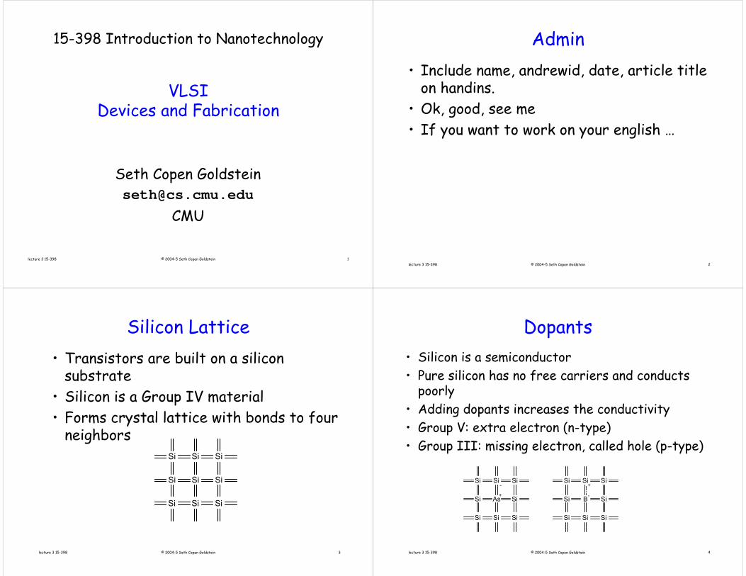
lecture 3 15-398 © 2004-5 Seth Copen Goldstein 1
VLSIDevices and Fabrication
Seth Copen [email protected]
CMU
15-398 Introduction to Nanotechnology
lecture 3 15-398 © 2004-5 Seth Copen Goldstein 2
Admin• Include name, andrewid, date, article title
on handins.• Ok, good, see me• If you want to work on your english …
lecture 3 15-398 © 2004-5 Seth Copen Goldstein 3
Silicon Lattice• Transistors are built on a silicon
substrate• Silicon is a Group IV material• Forms crystal lattice with bonds to four
neighbors
Si SiSi
Si SiSi
Si SiSi
lecture 3 15-398 © 2004-5 Seth Copen Goldstein 4
Dopants• Silicon is a semiconductor• Pure silicon has no free carriers and conducts
poorly• Adding dopants increases the conductivity• Group V: extra electron (n-type)• Group III: missing electron, called hole (p-type)
As SiSi
Si SiSi
Si SiSi
B SiSi
Si SiSi
Si SiSi
-
+
+
-
lecture 3 15-398 © 2004-5 Seth Copen Goldstein 5
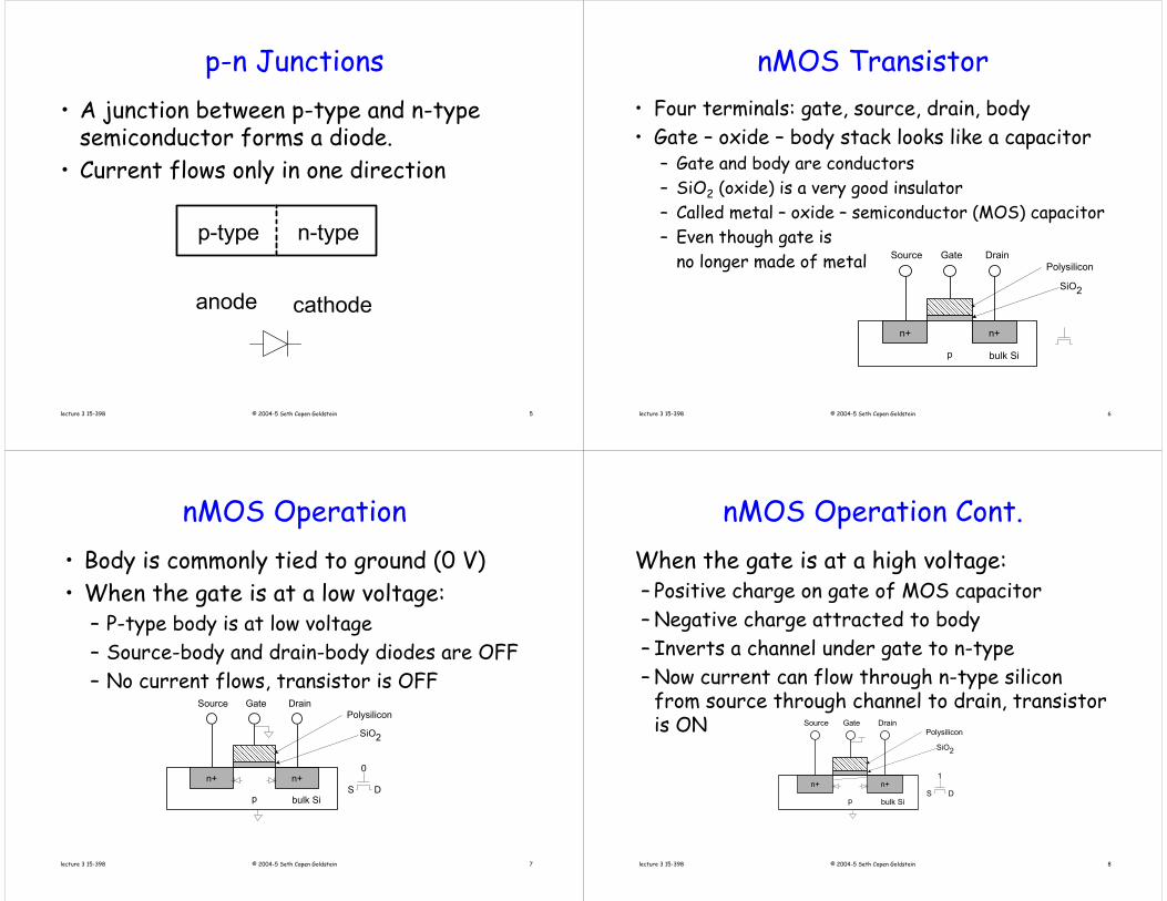
p-n Junctions• A junction between p-type and n-type
semiconductor forms a diode.• Current flows only in one direction
p-type n-type
anode cathode
lecture 3 15-398 © 2004-5 Seth Copen Goldstein 6
nMOS Transistor• Four terminals: gate, source, drain, body• Gate – oxide – body stack looks like a capacitor
– Gate and body are conductors– SiO2 (oxide) is a very good insulator– Called metal – oxide – semiconductor (MOS) capacitor– Even though gate is
no longer made of metal
n+
p
GateSource Drain
bulk Si
SiO2
Polysilicon
n+
lecture 3 15-398 © 2004-5 Seth Copen Goldstein 7
nMOS Operation• Body is commonly tied to ground (0 V)• When the gate is at a low voltage:
– P-type body is at low voltage– Source-body and drain-body diodes are OFF– No current flows, transistor is OFF
n+
p
GateSource Drain
bulk Si
SiO2
Polysilicon
n+D
0
S
lecture 3 15-398 © 2004-5 Seth Copen Goldstein 8
nMOS Operation Cont.When the gate is at a high voltage:– Positive charge on gate of MOS capacitor– Negative charge attracted to body– Inverts a channel under gate to n-type– Now current can flow through n-type silicon
from source through channel to drain, transistor is ON
n+
p
GateSource Drain
bulk Si
SiO2
Polysilicon
n+D
1
S
lecture 3 15-398 © 2004-5 Seth Copen Goldstein 9
pMOS Transistor• Similar, but doping and voltages reversed
– Body tied to high voltage (VDD)– Gate low: transistor ON– Gate high: transistor OFF– Bubble indicates inverted behavior
SiO2
n
GateSource Drain
bulk Si
Polysilicon
p+ p+
lecture 3 15-398 © 2004-5 Seth Copen Goldstein 10
Power Supply Voltage• GND = 0 V• In 1980’s, VDD = 5V• VDD has decreased in modern processes
– High VDD would damage modern tiny transistors
– Lower VDD saves power• VDD = 3.3, 2.5, 1.8, 1.5, 1.2, 1.0, …
lecture 3 15-398 © 2004-5 Seth Copen Goldstein 11
Transistors as Switches• We can view MOS transistors as
electrically controlled switches• Voltage at gate controls path from source
to drain
gs
d
g = 0
s
d
g = 1
s
d
gs
d
s
d
s
d
nMOS
pMOS
OFF ON
ON OFF
lecture 3 15-398 © 2004-5 Seth Copen Goldstein 12
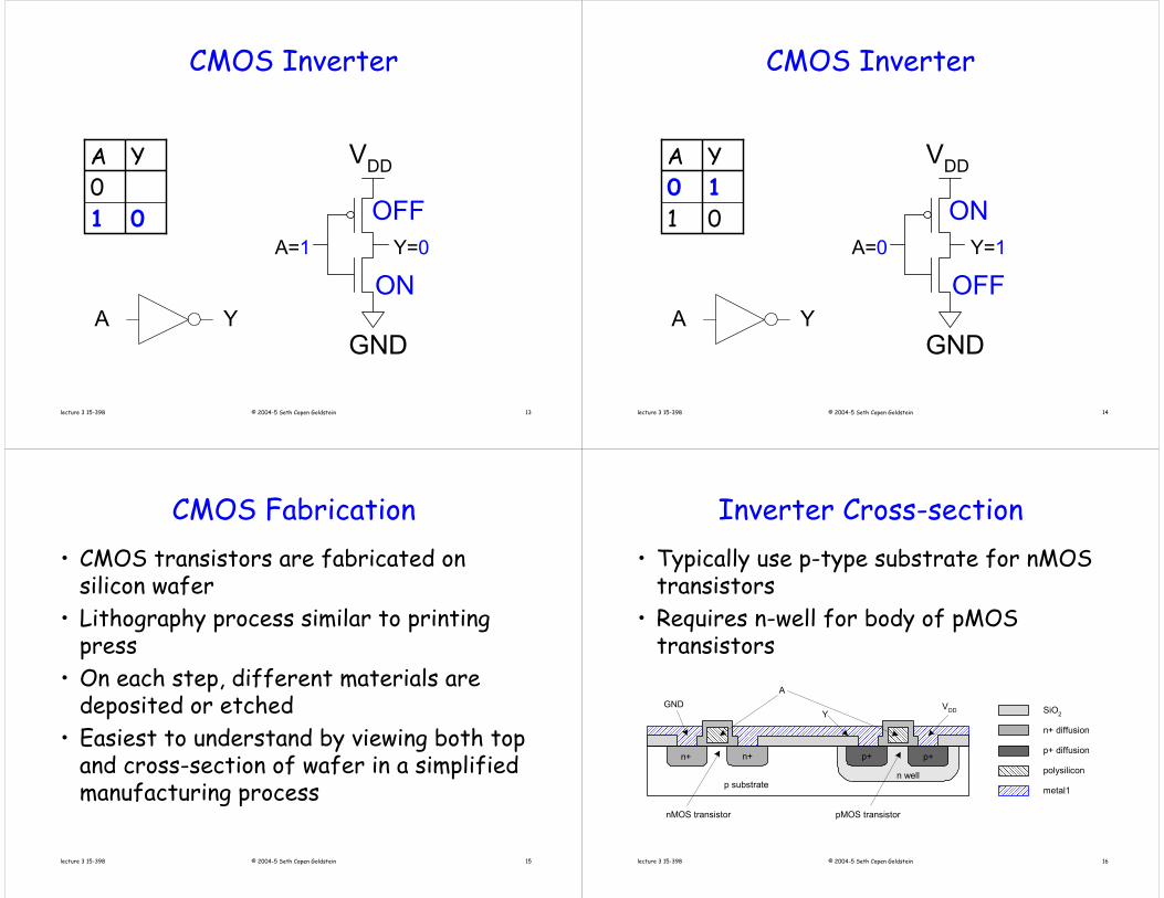
CMOS Inverter
10
YA VDD
A Y
GNDA Y
lecture 3 15-398 © 2004-5 Seth Copen Goldstein 13
CMOS Inverter
010
YA VDD
A=1 Y=0
GND
ON
OFF
A Y
lecture 3 15-398 © 2004-5 Seth Copen Goldstein 14
CMOS Inverter
0110YA VDD
A=0 Y=1
GND
OFF
ON
A Y
lecture 3 15-398 © 2004-5 Seth Copen Goldstein 15
CMOS Fabrication• CMOS transistors are fabricated on
silicon wafer• Lithography process similar to printing
press• On each step, different materials are
deposited or etched• Easiest to understand by viewing both top
and cross-section of wafer in a simplified manufacturing process
lecture 3 15-398 © 2004-5 Seth Copen Goldstein 16
Inverter Cross-section• Typically use p-type substrate for nMOS
transistors• Requires n-well for body of pMOS
transistors
n+
p substrate
p+
n well
A
YGND VDD
n+ p+
SiO2
n+ diffusion
p+ diffusion
polysilicon
metal1
nMOS transistor pMOS transistor
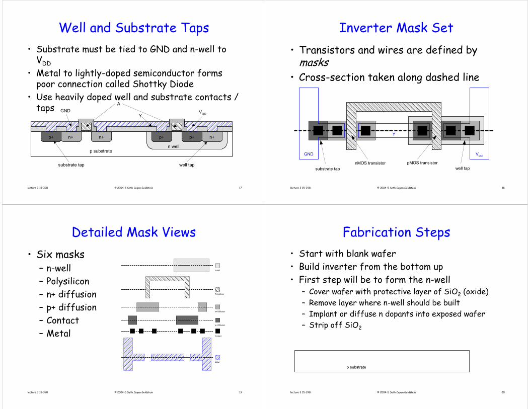
lecture 3 15-398 © 2004-5 Seth Copen Goldstein 17
Well and Substrate Taps• Substrate must be tied to GND and n-well to
VDD• Metal to lightly-doped semiconductor forms
poor connection called Shottky Diode• Use heavily doped well and substrate contacts /
taps
n+
p substrate
p+
n well
A
YGND VDD
n+p+
substrate tap well tap
n+ p+
lecture 3 15-398 © 2004-5 Seth Copen Goldstein 18
Inverter Mask Set• Transistors and wires are defined by
masks• Cross-section taken along dashed line
GND VDD
Y
A
substrate tap well tapnMOS transistor pMOS transistor
lecture 3 15-398 © 2004-5 Seth Copen Goldstein 19
Detailed Mask Views• Six masks
– n-well– Polysilicon– n+ diffusion– p+ diffusion– Contact– Metal
Metal
Polysilicon
Contact
n+ Diffusion
p+ Diffusion
n well
lecture 3 15-398 © 2004-5 Seth Copen Goldstein 20
Fabrication Steps• Start with blank wafer• Build inverter from the bottom up• First step will be to form the n-well
– Cover wafer with protective layer of SiO2 (oxide)– Remove layer where n-well should be built– Implant or diffuse n dopants into exposed wafer– Strip off SiO2
p substrate
lecture 3 15-398 © 2004-5 Seth Copen Goldstein 21
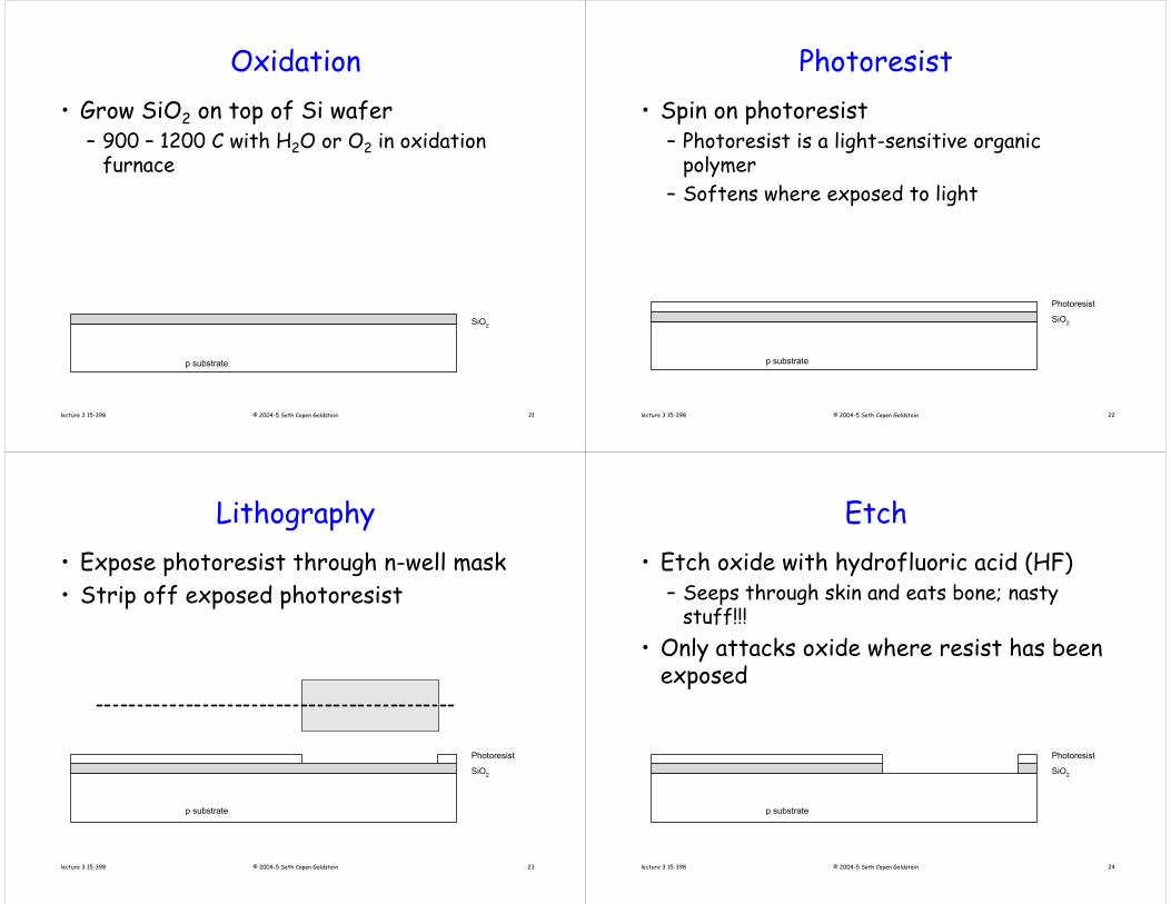
Oxidation• Grow SiO2 on top of Si wafer
– 900 – 1200 C with H2O or O2 in oxidation furnace
p substrate
SiO2
lecture 3 15-398 © 2004-5 Seth Copen Goldstein 22
Photoresist• Spin on photoresist
– Photoresist is a light-sensitive organic polymer
– Softens where exposed to light
p substrate
SiO2
Photoresist
lecture 3 15-398 © 2004-5 Seth Copen Goldstein 23
Lithography• Expose photoresist through n-well mask• Strip off exposed photoresist
p substrate
SiO2
Photoresist
lecture 3 15-398 © 2004-5 Seth Copen Goldstein 24
Etch• Etch oxide with hydrofluoric acid (HF)
– Seeps through skin and eats bone; nasty stuff!!!
• Only attacks oxide where resist has been exposed
p substrate
SiO2
Photoresist
lecture 3 15-398 © 2004-5 Seth Copen Goldstein 25
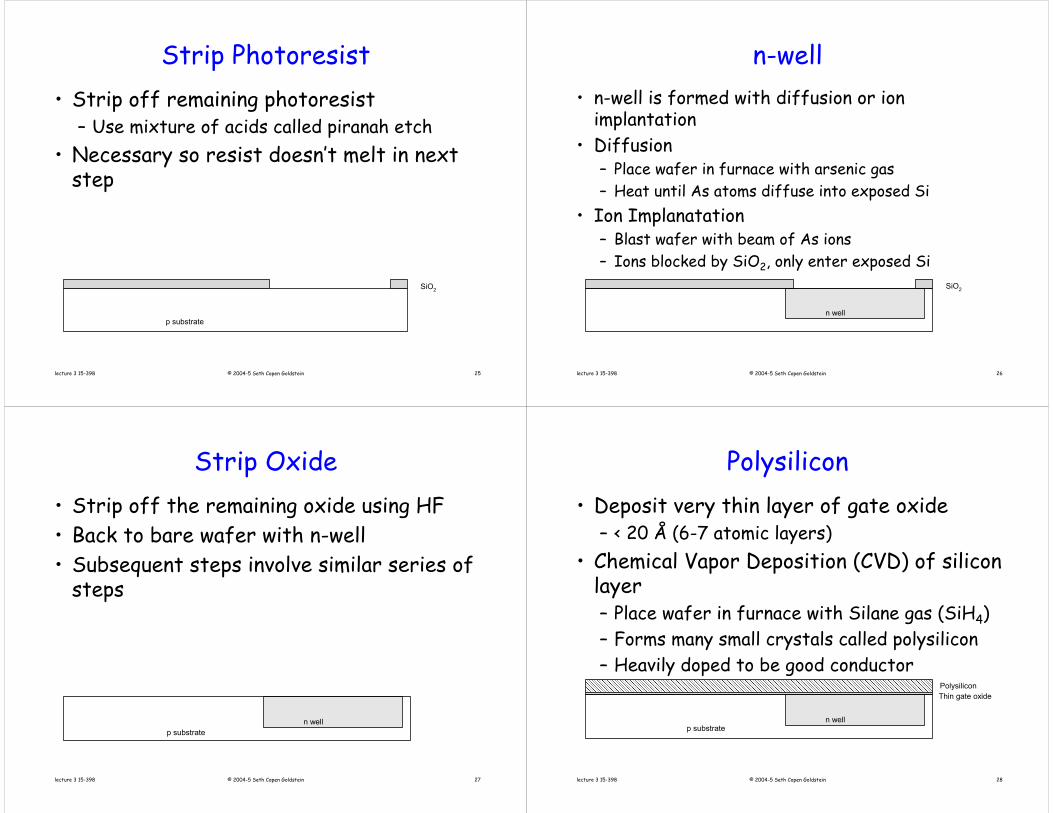
Strip Photoresist• Strip off remaining photoresist
– Use mixture of acids called piranah etch• Necessary so resist doesn’t melt in next
step
p substrate
SiO2
lecture 3 15-398 © 2004-5 Seth Copen Goldstein 26
n-well• n-well is formed with diffusion or ion
implantation• Diffusion
– Place wafer in furnace with arsenic gas– Heat until As atoms diffuse into exposed Si
• Ion Implanatation– Blast wafer with beam of As ions– Ions blocked by SiO2, only enter exposed Si
n well
SiO2
lecture 3 15-398 © 2004-5 Seth Copen Goldstein 27
Strip Oxide• Strip off the remaining oxide using HF• Back to bare wafer with n-well• Subsequent steps involve similar series of
steps
p substraten well
lecture 3 15-398 © 2004-5 Seth Copen Goldstein 28
Polysilicon• Deposit very thin layer of gate oxide
– < 20 Å (6-7 atomic layers)• Chemical Vapor Deposition (CVD) of silicon
layer– Place wafer in furnace with Silane gas (SiH4)– Forms many small crystals called polysilicon– Heavily doped to be good conductor
Thin gate oxidePolysilicon
p substraten well
lecture 3 15-398 © 2004-5 Seth Copen Goldstein 29
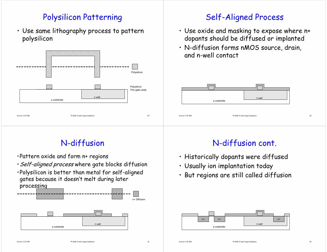
Polysilicon Patterning• Use same lithography process to pattern
polysilicon
Polysilicon
p substrate
Thin gate oxidePolysilicon
n well
lecture 3 15-398 © 2004-5 Seth Copen Goldstein 30
Self-Aligned Process• Use oxide and masking to expose where n+
dopants should be diffused or implanted• N-diffusion forms nMOS source, drain,
and n-well contact
p substraten well
lecture 3 15-398 © 2004-5 Seth Copen Goldstein 31
N-diffusion•Pattern oxide and form n+ regions•Self-aligned process where gate blocks diffusion•Polysilicon is better than metal for self-aligned gates because it doesn’t melt during later processing
p substraten well
n+ Diffusion
lecture 3 15-398 © 2004-5 Seth Copen Goldstein 32
N-diffusion cont.• Historically dopants were diffused• Usually ion implantation today• But regions are still called diffusion
n wellp substrate
n+n+ n+
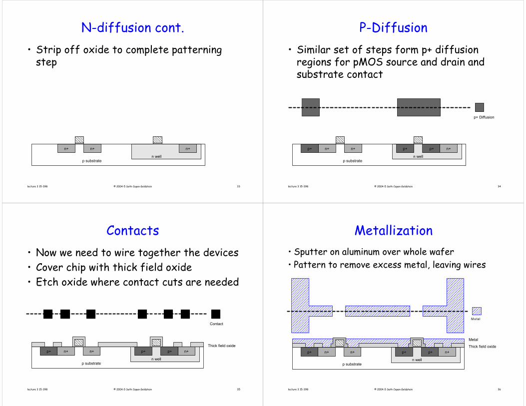
lecture 3 15-398 © 2004-5 Seth Copen Goldstein 33
N-diffusion cont.• Strip off oxide to complete patterning
step
n wellp substrate
n+n+ n+
lecture 3 15-398 © 2004-5 Seth Copen Goldstein 34
P-Diffusion• Similar set of steps form p+ diffusion
regions for pMOS source and drain and substrate contact
p+ Diffusion
p substraten well
n+n+ n+p+p+p+
lecture 3 15-398 © 2004-5 Seth Copen Goldstein 35
Contacts• Now we need to wire together the devices• Cover chip with thick field oxide• Etch oxide where contact cuts are needed
p substrate
Thick field oxide
n well
n+n+ n+p+p+p+
Contact
lecture 3 15-398 © 2004-5 Seth Copen Goldstein 36
Metallization• Sputter on aluminum over whole wafer• Pattern to remove excess metal, leaving wires
p substrate
Metal
Thick field oxide
n well
n+n+ n+p+p+p+
M etal
NSF/SRC Engineering Research Center for Environmentally Benign Semiconductor ManufacturingSorenson
37
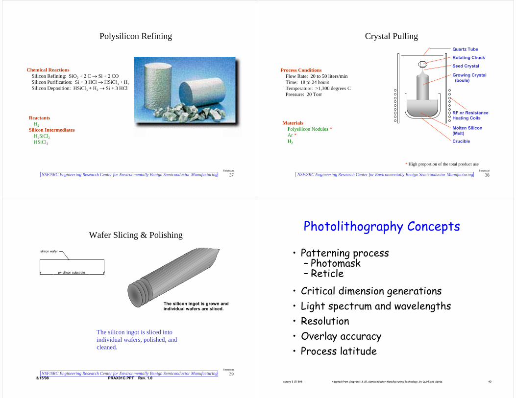
Polysilicon Refining
Chemical ReactionsSilicon Refining: SiO2 + 2 C → Si + 2 COSilicon Purification: Si + 3 HCl → HSiCl3 + H2Silicon Deposition: HSiCl3 + H2 → Si + 3 HCl
ReactantsH2
Silicon IntermediatesH2SiCl2HSiCl3
NSF/SRC Engineering Research Center for Environmentally Benign Semiconductor ManufacturingSorenson
38
Crystal PullingQuartz Tube
Rotating Chuck
Seed Crystal
Growing Crystal(boule)
RF or ResistanceHeating Coils
Molten Silicon(Melt)
Crucible
MaterialsPolysilicon Nodules *Ar *H2
* High proportion of the total product use
Process ConditionsFlow Rate: 20 to 50 liters/minTime: 18 to 24 hoursTemperature: >1,300 degrees CPressure: 20 Torr
NSF/SRC Engineering Research Center for Environmentally Benign Semiconductor ManufacturingSorenson
393/15/98 PRAX01C.PPT Rev. 1.0
Wafer Slicing & Polishing
The silicon ingot is grown and individual wafers are sliced.
The silicon ingot is sliced into individual wafers, polished, and cleaned.
silicon wafer
p+ silicon substrate
lecture 3 15-398 Adapted from Chapters 13-15, Semiconductor Manufacturing Technology, by Quirk and Serda 40
• Patterning process– Photomask– Reticle
• Critical dimension generations• Light spectrum and wavelengths• Resolution• Overlay accuracy• Process latitude
Photolithography Concepts
lecture 3 15-398 Adapted from Chapters 13-15, Semiconductor Manufacturing Technology, by Quirk and Serda 41
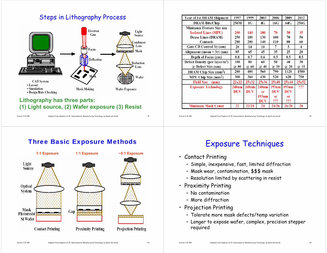
Steps in Lithography Process
Lithography has three parts:(1) Light source, (2) Wafer exposure (3) Resist
lecture 3 15-398 Adapted from Chapters 13-15, Semiconductor Manufacturing Technology, by Quirk and Serda 42
lecture 3 15-398 Adapted from Chapters 13-15, Semiconductor Manufacturing Technology, by Quirk and Serda 43
Three Basic Exposure Methods1:1 Exposure 1:1 Exposure ~5:1 Exposure
lecture 3 15-398 Adapted from Chapters 13-15, Semiconductor Manufacturing Technology, by Quirk and Serda 44
Exposure Techniques• Contact Printing
– Simple, inexpensive, fast, limited diffraction– Mask wear, contamination, $$$ mask– Resolution limited by scattering in resist
• Proximity Printing– No contamination– More diffraction
• Projection Printing– Tolerate more mask defects/temp variation– Longer to expose wafer, complex, precision stepper
required
lecture 3 15-398 Adapted from Chapters 13-15, Semiconductor Manufacturing Technology, by Quirk and Serda 45
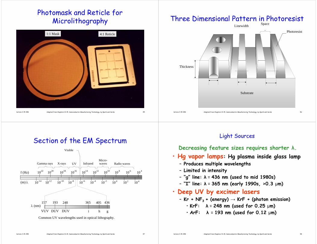
Photomask and Reticle for Microlithography
4:1 Reticle1:1 Mask
lecture 3 15-398 Adapted from Chapters 13-15, Semiconductor Manufacturing Technology, by Quirk and Serda 46
Three Dimensional Pattern in PhotoresistLinewidth Space
Thickness
Substrate
Photoresist
lecture 3 15-398 Adapted from Chapters 13-15, Semiconductor Manufacturing Technology, by Quirk and Serda 47
Section of the EM SpectrumVisible
Radio wavesMicro-wavesInfraredGamma rays UVX-rays
f (Hz) 1010101010101010 1010 4681012141622 1820
λ(m) 420-2-4-6-8-14 -10-12 1010101010101010 1010
365 436405248193157
ghiDUVDUVVUVλ (nm)
Common UV wavelengths used in optical lithography.
lecture 3 15-398 Adapted from Chapters 13-15, Semiconductor Manufacturing Technology, by Quirk and Serda 48
Light Sources
Decreasing feature sizes requires shorter λ.• Hg vapor lamps: Hg plasma inside glass lamp
– Produces multiple wavelengths– Limited in intensity– “g” line: λ = 436 nm (used to mid 1980s)– “I” line: λ = 365 nm (early 1990s, >0.3 μm)
• Deep UV by excimer lasers– Kr + NF3 + (energy) → KrF + (photon emission)
• KrF: λ = 248 nm (used for 0.25 μm)• ArF: λ = 193 nm (used for 0.12 μm)
lecture 3 15-398 Adapted from Chapters 13-15, Semiconductor Manufacturing Technology, by Quirk and Serda 49
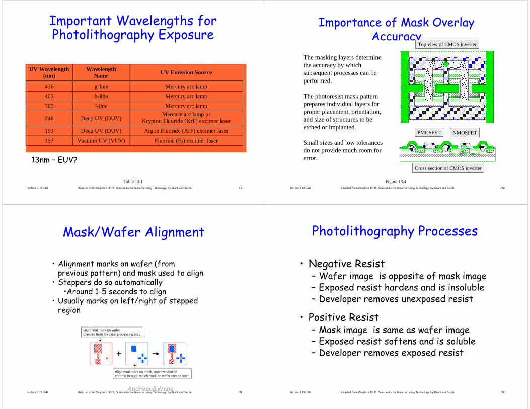
Important Wavelengths for Photolithography Exposure
UV Wavelength(nm)
WavelengthName UV Emission Source
436 g-line Mercury arc lamp
405 h-line Mercury arc lamp
365 i-line Mercury arc lamp
248 Deep UV (DUV)Mercury arc lamp or
Krypton Fluoride (KrF) excimer laser
193 Deep UV (DUV) Argon Fluoride (ArF) excimer laser
157 Vacuum UV (VUV) Fluorine (F2) excimer laser
Table 13.1
13nm – EUV?
lecture 3 15-398 Adapted from Chapters 13-15, Semiconductor Manufacturing Technology, by Quirk and Serda 50
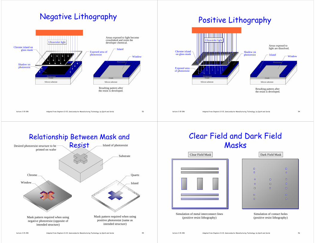
Importance of Mask Overlay Accuracy
PMOSFET NMOSFET
Cross section of CMOS inverter
Top view of CMOS inverter
The masking layers determine the accuracy by which subsequent processes can be performed.
The photoresist mask pattern prepares individual layers for proper placement, orientation, and size of structures to be etched or implanted.
Small sizes and low tolerances do not provide much room for error.
Figure 13.4
lecture 3 15-398 Adapted from Chapters 13-15, Semiconductor Manufacturing Technology, by Quirk and Serda 51
Mask/Wafer Alignment
Andreou&Wang
• Alignment marks on wafer (from previous pattern) and mask used to align
• Steppers do so automatically•Around 1-5 seconds to align
• Usually marks on left/right of stepped region
lecture 3 15-398 Adapted from Chapters 13-15, Semiconductor Manufacturing Technology, by Quirk and Serda 52
Photolithography Processes
• Negative Resist– Wafer image is opposite of mask image– Exposed resist hardens and is insoluble– Developer removes unexposed resist
• Positive Resist– Mask image is same as wafer image– Exposed resist softens and is soluble– Developer removes exposed resist
lecture 3 15-398 Adapted from Chapters 13-15, Semiconductor Manufacturing Technology, by Quirk and Serda 53
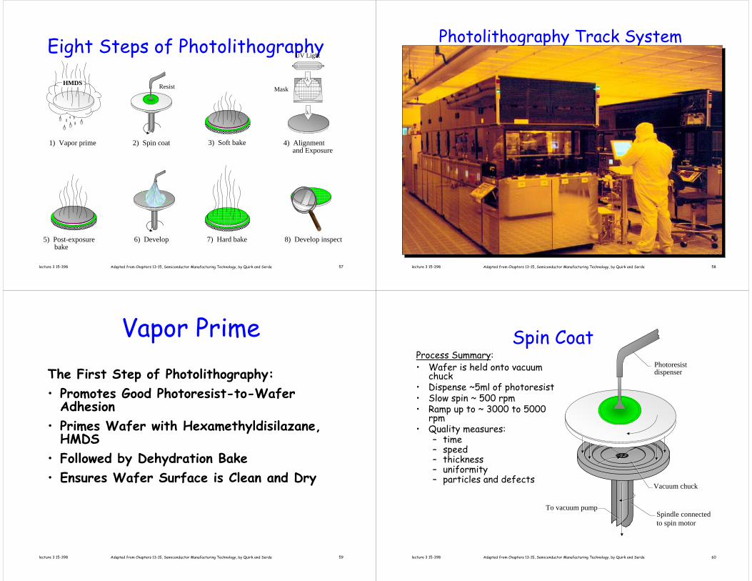
Negative Lithography
Ultraviolet lightUltraviolet light
Island
Areas exposed to light become crosslinked and resist the developer chemical.
Resulting pattern after the resist is developed.
Window
Exposed area of photoresist
Shadow on photoresist
Chrome island on glass mask
Silicon substrateSilicon substrate
PhotoresistPhotoresistOxideOxide
PhotoresistPhotoresist
OxideOxide
Silicon substrateSilicon substrate
lecture 3 15-398 Adapted from Chapters 13-15, Semiconductor Manufacturing Technology, by Quirk and Serda 54
Positive Lithography
photoresist
silicon substrate
oxide oxide
silicon substrate
photoresist
Ultraviolet lightUltraviolet light
Island
Areas exposed to light are dissolved.
Resulting pattern after the resist is developed.
Shadow on photoresist
Exposed area of photoresist
Chrome island on glass mask
Window
Silicon substrateSilicon substrate
PhotoresistPhotoresistOxideOxide
PhotoresistPhotoresist
OxideOxide
Silicon substrateSilicon substrate
lecture 3 15-398 Adapted from Chapters 13-15, Semiconductor Manufacturing Technology, by Quirk and Serda 55
Relationship Between Mask and ResistDesired photoresist structure to be
printed on wafer
Window
Substrate
Island of photoresist
QuartzChrome
Island
Mask pattern required when using negative photoresist (opposite of
intended structure)
Mask pattern required when using positive photoresist (same as
intended structure)
lecture 3 15-398 Adapted from Chapters 13-15, Semiconductor Manufacturing Technology, by Quirk and Serda 56
Clear Field and Dark Field Masks
Simulation of contact holes(positive resist lithography)
Simulation of metal interconnect lines(positive resist lithography)
Clear Field Mask Dark Field Mask
lecture 3 15-398 Adapted from Chapters 13-15, Semiconductor Manufacturing Technology, by Quirk and Serda 57
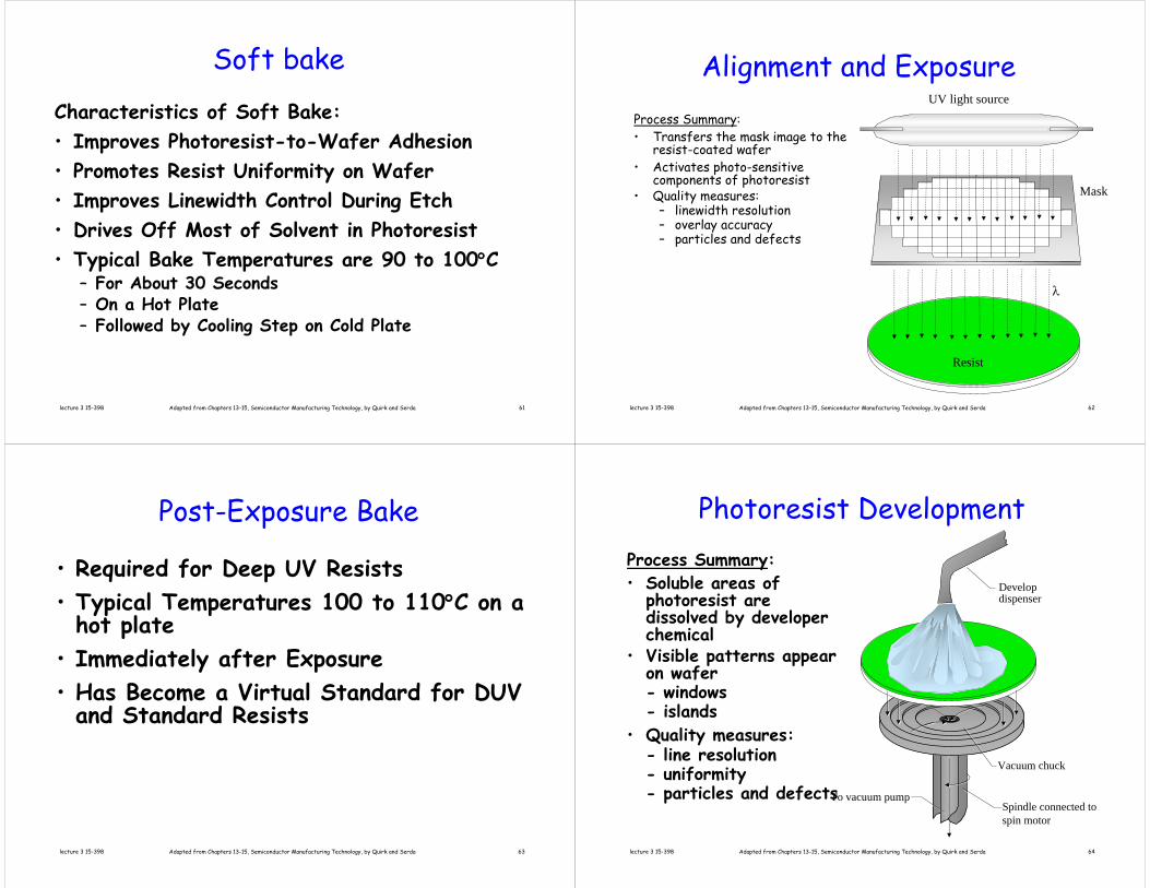
Eight Steps of Photolithography
8) Develop inspect5) Post-exposure bake
6) Develop 7) Hard bake
UV Light
Mask
λ
λ
4) Alignmentand Exposure
Resist
2) Spin coat 3) Soft bake1) Vapor prime
HMDS
lecture 3 15-398 Adapted from Chapters 13-15, Semiconductor Manufacturing Technology, by Quirk and Serda 58
Photolithography Track System
lecture 3 15-398 Adapted from Chapters 13-15, Semiconductor Manufacturing Technology, by Quirk and Serda 59
Vapor PrimeThe First Step of Photolithography:• Promotes Good Photoresist-to-Wafer
Adhesion• Primes Wafer with Hexamethyldisilazane,
HMDS• Followed by Dehydration Bake• Ensures Wafer Surface is Clean and Dry
lecture 3 15-398 Adapted from Chapters 13-15, Semiconductor Manufacturing Technology, by Quirk and Serda 60
Spin CoatProcess Summary:• Wafer is held onto vacuum
chuck• Dispense ~5ml of photoresist• Slow spin ~ 500 rpm• Ramp up to ~ 3000 to 5000
rpm• Quality measures:
– time– speed– thickness– uniformity– particles and defects
Vacuum chuck
Spindle connected to spin motor
To vacuum pump
Photoresist dispenser
lecture 3 15-398 Adapted from Chapters 13-15, Semiconductor Manufacturing Technology, by Quirk and Serda 61
Soft bake
Characteristics of Soft Bake:• Improves Photoresist-to-Wafer Adhesion• Promotes Resist Uniformity on Wafer• Improves Linewidth Control During Etch• Drives Off Most of Solvent in Photoresist• Typical Bake Temperatures are 90 to 100°C
– For About 30 Seconds– On a Hot Plate– Followed by Cooling Step on Cold Plate
lecture 3 15-398 Adapted from Chapters 13-15, Semiconductor Manufacturing Technology, by Quirk and Serda 62
Alignment and ExposureProcess Summary:• Transfers the mask image to the
resist-coated wafer• Activates photo-sensitive
components of photoresist• Quality measures:
– linewidth resolution– overlay accuracy– particles and defects
UV light source
Mask
Resist
λ
lecture 3 15-398 Adapted from Chapters 13-15, Semiconductor Manufacturing Technology, by Quirk and Serda 63
Post-Exposure Bake
• Required for Deep UV Resists• Typical Temperatures 100 to 110°C on a hot plate
• Immediately after Exposure• Has Become a Virtual Standard for DUV and Standard Resists
lecture 3 15-398 Adapted from Chapters 13-15, Semiconductor Manufacturing Technology, by Quirk and Serda 64
Photoresist DevelopmentProcess Summary:• Soluble areas of
photoresist are dissolved by developer chemical
• Visible patterns appear on wafer- windows- islands
• Quality measures:- line resolution- uniformity- particles and defects
Vacuum chuck
Spindle connected to spin motor
To vacuum pump
Develop dispenser
lecture 3 15-398 Adapted from Chapters 13-15, Semiconductor Manufacturing Technology, by Quirk and Serda 65
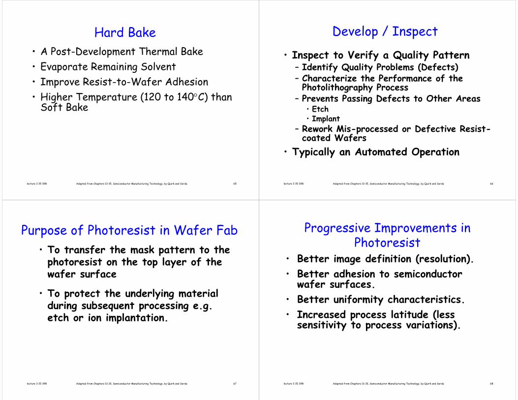
Hard Bake• A Post-Development Thermal Bake• Evaporate Remaining Solvent• Improve Resist-to-Wafer Adhesion• Higher Temperature (120 to 140°C) than
Soft Bake
lecture 3 15-398 Adapted from Chapters 13-15, Semiconductor Manufacturing Technology, by Quirk and Serda 66
Develop / Inspect
• Inspect to Verify a Quality Pattern– Identify Quality Problems (Defects)– Characterize the Performance of the Photolithography Process
– Prevents Passing Defects to Other Areas• Etch• Implant
– Rework Mis-processed or Defective Resist-coated Wafers
• Typically an Automated Operation
lecture 3 15-398 Adapted from Chapters 13-15, Semiconductor Manufacturing Technology, by Quirk and Serda 67
Purpose of Photoresist in Wafer Fab• To transfer the mask pattern to the photoresist on the top layer of the wafer surface
• To protect the underlying material during subsequent processing e.g. etch or ion implantation.
lecture 3 15-398 Adapted from Chapters 13-15, Semiconductor Manufacturing Technology, by Quirk and Serda 68
Progressive Improvements in Photoresist
• Better image definition (resolution).• Better adhesion to semiconductor
wafer surfaces.• Better uniformity characteristics.• Increased process latitude (less
sensitivity to process variations).
lecture 3 15-398 Adapted from Chapters 13-15, Semiconductor Manufacturing Technology, by Quirk and Serda 69
• Photoresist– Types of Photoresist– Negative Versus Positive Photoresists
• Photoresist Physical Properties• Conventional I-Line Photoresists
– Negative I-Line Photoresists– Positive I-Line Photoresists
• Deep UV (DUV) Photoresists• Photoresist Dispensing Methods
Spin Coat
lecture 3 15-398 Adapted from Chapters 13-15, Semiconductor Manufacturing Technology, by Quirk and Serda 70
Types of Photoresists
• Two Types of Photoresist– Positive Resist– Negative Resist
• CD Capability– Conventional Resist– Deep UV Resist
• Process Applications– Non-critical Layers– Critical Layers
lecture 3 15-398 Adapted from Chapters 13-15, Semiconductor Manufacturing Technology, by Quirk and Serda 71
Negative Versus Positive Resists
• Negative Resist– Wafer image is opposite of mask image– Exposed resist hardens and is insoluble– Developer removes unexposed resist
• Positive Resist– Mask image is same as wafer image– Exposed resist softens and is soluble– Developer removes exposed resist
• Resolution Issues• Clear Field Versus Dark Field Masks
lecture 3 15-398 Adapted from Chapters 13-15, Semiconductor Manufacturing Technology, by Quirk and Serda 72
Photoresist Physical Characteristics
ResolutionContrastSensitivityViscosityAdhesionEtch resistanceSurface tensionStorage and handlingContaminants and particles
lecture 3 15-398 Adapted from Chapters 13-15, Semiconductor Manufacturing Technology, by Quirk and Serda 73
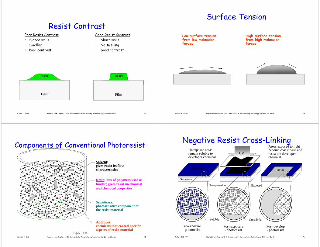
Resist ContrastPoor Resist Contrast• Sloped walls• Swelling• Poor contrast
Resist
Film
Good Resist Contrast• Sharp walls• No swelling• Good contrast
Resist
Film
lecture 3 15-398 Adapted from Chapters 13-15, Semiconductor Manufacturing Technology, by Quirk and Serda 74
Surface Tension
Low surface tension High surface tensionfrom low molecular from high molecular forces forces
lecture 3 15-398 Adapted from Chapters 13-15, Semiconductor Manufacturing Technology, by Quirk and Serda 75
Components of Conventional Photoresist
Additives: chemicals that control specific aspects of resist material
Solvent: gives resist its flow characteristics
Sensitizers: photosensitive component of the resist material
Resin: mix of polymers used as binder; gives resist mechanical and chemical properties
Figure 13.18lecture 3 15-398 Adapted from Chapters 13-15, Semiconductor Manufacturing Technology, by Quirk and Serda 76
Negative Resist Cross-LinkingAreas exposed to light become crosslinked and resist the developer chemical.
Unexposed areas remain soluble to developer chemical.
Pre-exposure- photoresist
Post-exposure- photoresist
Post-develop- photoresist
UV
OxidePhotoresist
Substrate
Crosslinks
Unexposed Exposed
Soluble
lecture 3 15-398 Adapted from Chapters 13-15, Semiconductor Manufacturing Technology, by Quirk and Serda 77
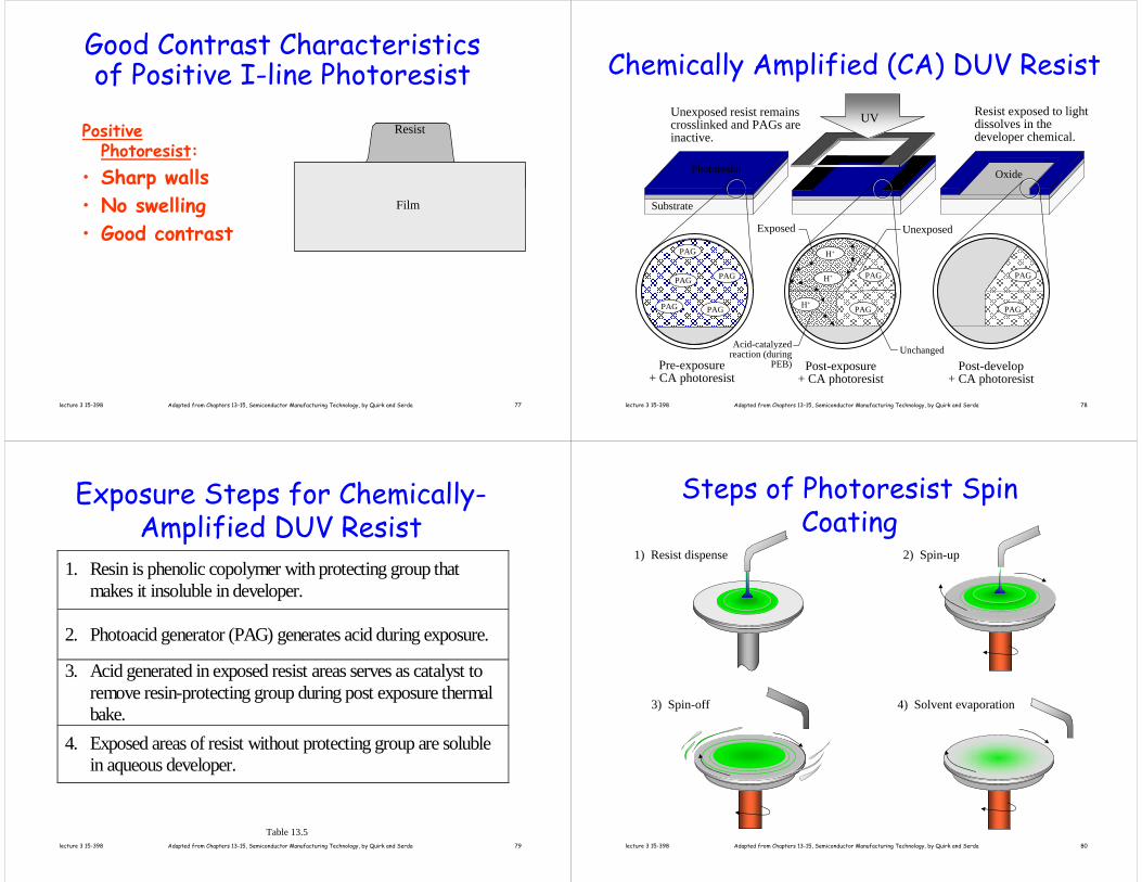
Good Contrast Characteristics of Positive I-line Photoresist
Positive Photoresist:
• Sharp walls• No swelling• Good contrast
Film
Resist
lecture 3 15-398 Adapted from Chapters 13-15, Semiconductor Manufacturing Technology, by Quirk and Serda 78
Chemically Amplified (CA) DUV ResistResist exposed to light dissolves in the developer chemical.
Unexposed resist remains crosslinked and PAGs are inactive.
Pre-exposure+ CA photoresist
Post-exposure+ CA photoresist
Post-develop+ CA photoresist
UV
OxidePhotoresist
Substrate
Unchanged
Exposed Unexposed
Acid-catalyzed reaction (during
PEB)
PAG
PAG
PAGPAG
H+
PAG
PAG
PAG
H+
H+ PAG
PAG
lecture 3 15-398 Adapted from Chapters 13-15, Semiconductor Manufacturing Technology, by Quirk and Serda 79
Exposure Steps for Chemically-Amplified DUV Resist
1. Resin is phenolic copolymer with protecting group thatmakes it insoluble in developer.
2. Photoacid generator (PAG) generates acid during exposure.
3. Acid generated in exposed resist areas serves as catalyst toremove resin-protecting group during post exposure thermalbake.
4. Exposed areas of resist without protecting group are solublein aqueous developer.
Table 13.5lecture 3 15-398 Adapted from Chapters 13-15, Semiconductor Manufacturing Technology, by Quirk and Serda 80
Steps of Photoresist Spin Coating
3) Spin-off 4) Solvent evaporation
1) Resist dispense 2) Spin-up
lecture 3 15-398 Adapted from Chapters 13-15, Semiconductor Manufacturing Technology, by Quirk and Serda 81
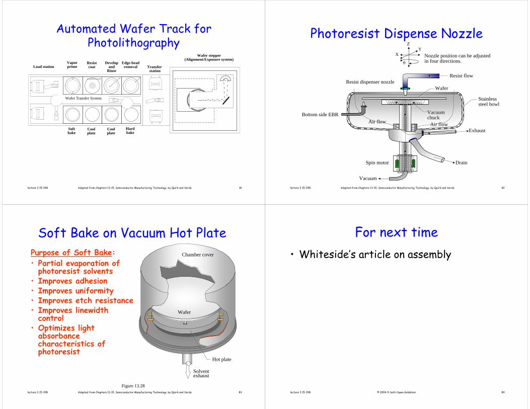
Wafer Transfer System
Load station Transferstation
Vapor prime
Resist coat
Develop and
Rinse
Edge-bead removal
Soft bake
Cool plate
Cool plate
Hard bake
Wafer stepper (Alignment/Exposure system)
Automated Wafer Track for Photolithography
lecture 3 15-398 Adapted from Chapters 13-15, Semiconductor Manufacturing Technology, by Quirk and Serda 82
Photoresist Dispense NozzleZ
YX
θ
Resist dispenser nozzle
Bottom side EBR
Vacuum
Vacuum chuckVacuum chuck
Spin motor
WaferWafer
Exhaust
Drain
Resist flowResist flow
Stainless steel bowl
Air flowAir flow Air flowAir flow
Nozzle position can be adjusted in four directions.
lecture 3 15-398 Adapted from Chapters 13-15, Semiconductor Manufacturing Technology, by Quirk and Serda 83
Soft Bake on Vacuum Hot PlatePurpose of Soft Bake:• Partial evaporation of
photoresist solvents• Improves adhesion• Improves uniformity• Improves etch resistance• Improves linewidth
control• Optimizes light
absorbance characteristics of photoresist
Hot plate
Wafer
Solvent exhaust
Chamber cover
Figure 13.28lecture 3 15-398 © 2004-5 Seth Copen Goldstein 84
For next time• Whiteside’s article on assembly


![arXiv:1707.00589v2 [cond-mat.str-el] 19 Apr 2018€¦ · Quantitative characterization of the nanoscale local lattice strain induced by Sr dopants in La 1:92Sr 0:08CuO 4 J. Q. Lin,1,2](https://img.pdfslide.net/doc/110x75/600264487c9dd07a4f37d21f/arxiv170700589v2-cond-matstr-el-19-apr-2018-quantitative-characterization-of.jpg)


![arXiv:1207.1884v1 [cond-mat.mes-hall] 8 Jul 2012 · Coupling and coherent electrical control of two dopants in a silicon nanowire E. Dupont-Ferrier, 1B. Roche, B. Voisin, X. Jehl,1](https://img.pdfslide.net/doc/110x75/5bb5281809d3f24d6c8c82e4/arxiv12071884v1-cond-matmes-hall-8-jul-2012-coupling-and-coherent-electrical.jpg)