Embed Size (px)
Citation preview

~-------
1 11 ' ' ' ,. ' 1· '! - ! ' ~
'.1;d_l JJ_I ill '. ~I !r· ' I ' -[,:.; r. 11 : . l \ : , t
'~-·· ',- •. ,' '-c
·. 11·.;•:.I 11 ''. I !.,,' -~ .. :: l i -[ l /.· I .,, ... ' ... [, ' I I 1J ... /,_. _} • i
--- •.. . ..
i i '. i_ . ___ 1 _.i '_ 1,\.1 i. IJ : -r_-. ·-'-. 1./. ,r _1_1 -.:lL .~ .J,}_,,i

SOLID STATE NOVELTY PROJECTS

SOLID STATE NOVELTY PROJECTS
compiled by
M.H. BABANI, B.Sc.(Eng.)
BERNARDS [publishers) LTD The Grampians ,
Shepherds Bush Road London W67NF
England.
Although every care is taken with the preparation of this book, the publishers or author will not be responsible in any way for any errors that might occur.
The compiler of this book wishes to express his most sincere thanks to "ELECTRONICS AUSTRALIA", the leading radio, T.V. and_ electronics magazine published in that continent and to Sungravure Syndication, their agents, for permission to use some of the material in this book which appeared originally as articles in that magazine.
© 197 6 MICHAEL HARRY BAB AN I
I.S.B.N. 0 900162 60 0
First Published - July 1976
Printed and Manufactured in Great Britain by C. Nicholls & Co. Ltd.
CONTENTS
The Incredlble Optomin ..•....•.••................ 7
Water Warbler for Healthy Pot Plants ..•.•.•. '• • , •.•.•.... 21
Patch Panel for Op Amp Experiments .............•.... 24
Crystal Locked Musical Tone Generator .......... ,- .•.... 28
Novel LED's and Ladders Game ...••••....•.....•.... 42
"Magic" Table Lamp uses Low-Cost Touch Switch ....••••... 51
Low-Cost Alarm Sensor ........•....•............ 63
An Electronic Roulette Wheel. •....•..•.....•....... 66
A Simple Electronic Mosquito Repeller ....•..•....•.... 79
Automatic Lamp Dimmer ...... , ......•••.....•... 82
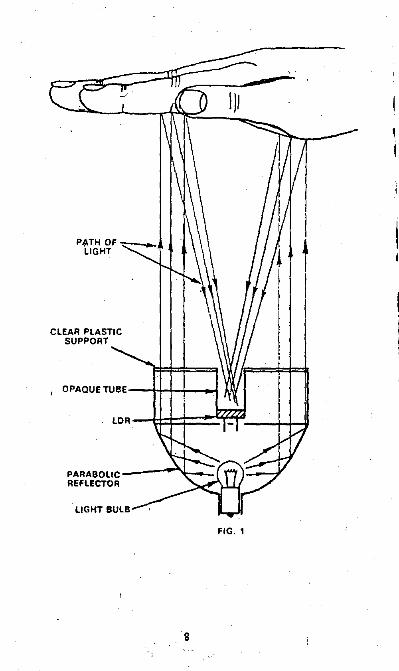
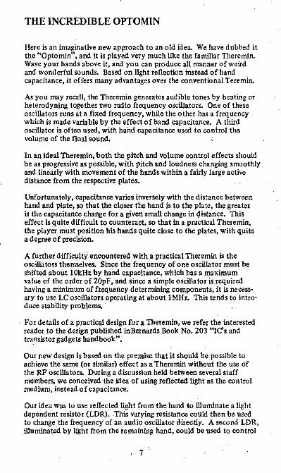
CLEAR PLASTIC SUPPORT
8
FIG. 1
I t
I l
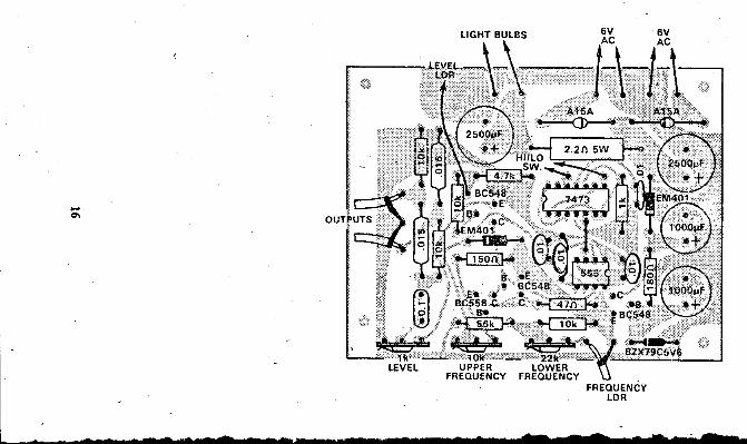
THE INCREDIBLE OPTOMIN
Here is an imaginative new approach to an old idea. We have dubbed it the "Optomin", and it is played very much like the familiar Theremin. Wave your hands above it, and you can produce all manner of weird and wonderful sounds.· Based on light reflection instead of hand capacitance, it offers many advantages over the conventional Teremin.
As you may recall, the Theremin generates audible tones by beating or heterodyning together two radio frequency oscillators. One of these oscillators runs at a fixed frequency, while the other has a frequency which is made varla ble by the effect of hand capacitance .. f',- third oscillator is often used, with hand capacitance used to control the volume of the final sound.
In an ideal Theremin, both the pitch and volume control effects should be as progressive as possible, with pitch and loudness changing smoothly and linearly with movement of the hands within a fairly large active distance from the respective plates.
Unfortunately, capacitance varies inversely with the distance between hand and plate, so that the closer the hand is to the plate, the greater is the capacitance change for a given small change in <)istance. This effect is quite difficult to counteract, so that in a practical Theremin, the player must position his hands quite close to the plates, with quite a degree of precision.
A further difficulty encountered with a practical Theremin is the oscillators themselves. Since the frequency of one oscillator must be shifted about 1 Ok Hz by hand capacitance, which has a maximum value of the order of 20pF, and since a simple oscillator is required having a minimum of frequency determining components, it is necessary to use LC oscillators operating at about 1 MHz. This tends to introduce stability problems.
For details of a practical design for a Theremin, we refer the interested reader to the design published inBernards Book No. 203 "!C's and transistor gadgets handbook".
Our new design is based on the premise that it should be possible to achieve the same (or similar} effect as a Theremin without the use of the RF oscillators. During a discussion held between several staff members, we conceived the idea of using reflected light as the control medium, instead of capacitance.
Our idea was to use reflected light from the hand to illuminate a light dependent resistor (LDR}. This varying resistance could then be used to change the frequency·of an audio oscillator directly. A second LDR, illuminated by light from the remaining hand, could be used to control
' 7
the output level of the oscillator. Thus was born the basic idea behind our light operated Thetemin, or OPTOMJN.
The next step was to see if the idea was practical, and if it could be implemented in a simple and economic way. So we devised a scheme to illuminate an LDR with light reflected from a hand, and examined the resulting characteristic.
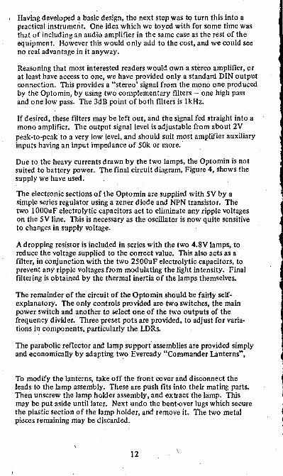
Figure I shows the general arrangement of the scheme devised. The LDR is mounted in a suitable sized opaque tube, sealed so that light can only enter from the open top end. This is mounted in a transparent plastic support, and positioned in the centre of a parabolic reflector. Light from the lamp is reflected upwards in a parallel beam. When a hand is placed above the LDR, light is reflected back down into it.
The amount of light reaching the LDR is dependent on the positioning of the hand. More light is reflected as the hand is lowered, until a point is reached where the hand starts to shield the LDR.
'In terms of the resistance of the LDR, this means that when the hand is well above the LDR, the resistanee is quite high. The actual value will depend on ambient light, but more about this later. As the hand is lowered, the resistance decreases, till the point is reached at which maximum light is being reflected into the tube. The actual minimum resistance will depend on a number of factors, including the reflectivity of the hand and the intensity of the light. Under actual operating conditions, the practical maximum resistarice of the LDR will be about 1 megohm. This will be because of ambient light entering the tube and reaching the LDR. This effect can be minimised by painting the inside of the tube flat black.
Tests on a prototype reflector and LDR assembly showed that a practical configuration could be constructed which gave a resistance change from about 100k to about 100 ohms. This is a range of 1000 to I, so.that provided suitable control circuits could be designed, we realised that it should be possible to obtain a frequency range extending over the full audio range, and with a large dynamic range.
Initial experiments were conducted using a programmable unijunction transistor (PUT) as a resistance controlled variable oscillator, but these were not successful, as a reliable oscillator with the required sweep range of I 000 to I could not be achieved.
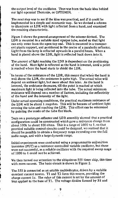
We then turned our attention to the ubiquitous 555 timer chip, this time with more success. The basic circuit is shown in Figure 2.
The 555 is connected as an astable multivibrator, driven by a variable constant current source. Tl and T2 form this source, providing the charge current I c. The value of this current is set by the amount of bias applied to the base of Tl. The voltage divider formed by RI and
9
..-------<>-----------------~-+ lDR A
4 8
R2 01 Rd 555 ,lflllf"
• lo½ 2 ,
C
FIG 2
+
Tl
FIG. 3
10
R2 is set so that when the LDR has a high resistance, Tl/T2 is biased on, and supplies maximum charge current.
As the resistance of the LDR is reduced, the bias on Tl is also reduced, decreasing the charging current Jc. If the LDR resistance is reduced enough, Tl/T2 will be cut-off, and no charging current will flow. This can be avoided by placing a suitable resistance in series with the LDR.
The charging current Jc flows into the timing capacitor C via DI, bypassing the discharge resistor. This means that the on-time of the 555 is determined solely by the LDR and the current generator. When the voltage across the capacitor C reaches two•thirds of the supply voltage, pin 7 is grounded, and C is discharged through Rd, the discharge resistor.
When the voltage has fallen to one-third of the supply voltage, the cycle is repeated again, with C being charged via DI by le. The output signai obtained at pin 3, is a train of negative going pulses, whose duration depends solely on Rd and C, and whose spacing is set by the LDR and the current generator.
The value of Re is chosen so that when the LDR has a large resistance, and le is at a maximum, the charge time is of the same order as the discharge time. This means that the upper frequency of the oscillator can be adjusted by varying Rd. If it is desired to alter the frequency over a greater range than possible by this means, C may be altered.
The lower frequency of the oscillator Is adiusted by means of the resistor in series with the LDR, mentic,ned previously. With this circuit, it was possible to obtain a frequency range in excess of 1000 to I.
The 555 output is a train of pulses, with a very large variation in spac!ng. This would not be very good to listen to, as it would consist mainly of high frequencies. To- avoid this, we have made the basic oscillator operate between 40kHz and 40Hz, and halved the frequency using a TTL flip-flop divider. This gives a squarewave output. The flip-flop se1ected is the 7473, which is actually a dual flip-flop. The second element is thus available to provide an alternative ulow" output.
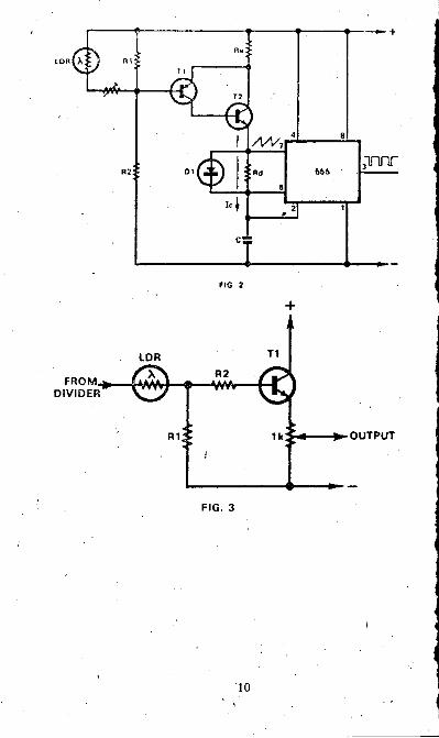
The volume control stage, used to give a large dynamic range, is rather unusual. Flgure 3 shows the basic idea. When the LDR resistance is large, the base of Tl is held low by RI and R2, so that Tl is held off, and no output is obtained.
Conversely, when the LDR resistance is low, the flip-flop output signal is coupled to the base of TI, which is then switched on and off. The output signal is taken from the potential divider in the emitter.
When the LDR has an intermediate value of resistance, Tl is only partially turned on, and so the output signal level is not as great. Thus the output signal can be varied from a maximum value to zero, in theory giving an infinite dynamic range.
11
Having developed a basic design, the next step was to turn this into a practical instrument. One idea which we toyed with for some time was that of including an audio amplifier in the same case as the rest of the equipment. However this would only add to the cost, and we could see no real advantage in it anyway.
Reasoning that most interested readers would own a stereo amplifier, or at least have access to one, we have provided only a standard DIN output connection. This provides a ustereo' signal from the mono one produced by the Optomin, by using two complementary filters - one high pass and one low pass. The 3dB point of both filters is lkHz.
If desired, these filters may be left out, and the signal fed straight into a mono amplifier. The output signal level is adjustable from about 2V peak-to-peak to a very low level, and should suit most amplifier auxiliary inputs having an input impedance of 50k or more.
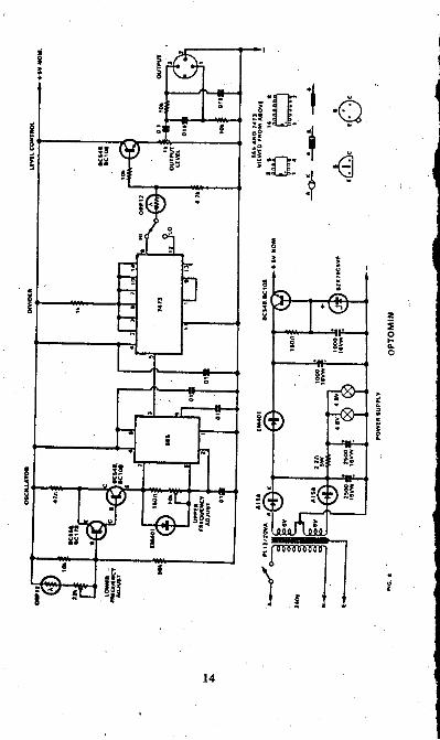
Due to the heavy currents drawn by the two tamps, the Optomin is not suited to battery power. The final circuit diagram, Figure 4, shows the supply we have used.
The electronic sections of the Optomin are supplied with SV by a simple series regulator using a zener diode and NPN transistor. The two 1 0O0uF electrolytic capacitors act to eliminate any ripple voltages on the SV line. This is necessary as the oscillator is now quite sensitive to changes in supply voltage.
A dropping resistor is includ_ed in series with the two 4.SV lamps, to reduce the voltage supplied to the correct value. This also acts as a filter, in conjunction with the two 2500uF electrolytic capacitors, to prevent any ripple voltages from modulating the light intensity. Final filtering is obtained by the thermal inertia of the lamps themselves.
The remainder of the circuit of the Optomin should be fairly selfexplanatory. The only controls provided are two switches, the main power switch and another to select one of the two outputs of the frequency divider. Three preset pots are provided, to adjust for variations in components, particularly the LDRs.
The parabolic reflector and lamp support assemblies are provided simply and economically by adapting two Eveready "Commander Lanterns",
To modify the lanterns, take off the front cover and disconnect the leads to the lamp assembly. These are push fits into their mating parts. Then unscrew the lamp holder assembly, and extract the lamp. This may be put aside until later. Next undo the bent-over lugs which secure the plastic section of the lamp holder, and remove it. The two metal pieces remaining may be discarded.
12
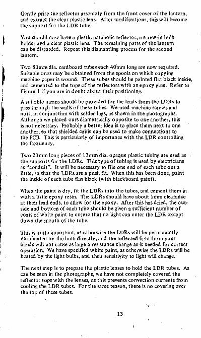
Gently prise the reflector assembly from the front cover of the lantern, and extract the clear plastic lens. After modifications, this will become the support for the LOR tube.
You should now have a plastic parabolic reflector, a screw-in bulb holder and a clear plastic lens. The remaining parts of the lantern can be discarded. Repeat this dismantling process for the second lantern.
Two 80mm dia. cardboard tubes each 40mm long are now required. Suitable ones may be obtained from the spools on which copying
, machine paper is wound. These tubes should be painted flat black inside, and cemented to the tops of the reflectors with an epoxy glue. Refer to Figure I if you are in doubt about their positioning.
A suitable means should be provided for the leads from the LDRs to pass through the walls of these tubes. We used machine screws and nuts, in conjunction with solder lugs, as shown in the photographs. Although we placed ours diametrically opposite to one another, this is not necessary. Probably a better idea is to place them next to one another, so that shielded cable can be used to make connections to the PCB. This is particularly of importance With the LOR controlling the frequency.
Two 20mm long pieces of 13mm dia. opaque plastic tubing are used as the supports for the LO Rs. This type of tubing is used by electricians as "conduit". It will be necessary to file one end of each tube out a little, so that the LDRs are a push fit. When this has been done, paint the inside of each tube flat black (with blackboard paint).
When the paint is dry, fit the.LO Rs into the tubes, and cement them in with a little epoxy resin. The LORs should have about Imm clearance at their lead ends, to allow for the epoxy. After this has dried, the outside and bottom of each tube should be given a sufficient oumber of coats of white paint to ensure that no light can enter the LOR except down the mouth of the tube.
This is quite important, as otherwise the LO Rs will be permanently illuminated by the bulb directly, and the reflected light from your hands will not cause as large a resistance change as is needed for correct operation. We have specified white paint, as otherwise the LO Rs will be heated by the light bulbs, and their sensitixity to light will change.
The next step is to prepare the plastic lenses to hold the LOR tubes. As can be seen in the photographs, we have not completely covered the reflector tops with the lenses, as this prevents convection currents from cooling the LOR tubes. For the same reason, there is no covering over the top of these tubes.
'•
13
·o· ·~ ·O f ~, f ::1 :! ...
l 00
~ :! •g :E
~ :. u
" ~~ ·• ·o· ~ . - :f
I : •
. . ! g ¥ i • i
~ z i
§f 0 .. ..
-= 0
•
i §f ••
I ~ ~~
14
The lenses from the lanterns are cut (with a hack-saw or similar tool) into 30mm wide strips, and a circular hole of the same diameter as the outside of the LDR tubes i.s made in the midd)e. Once this has been done, the LDR tubes can be glued in position with epoxy cement.
Thin hookup wire can now be used to conne,t between the LDR leads and the inner solder lugs of the cardboard tubes. Before attempting to solder to the LDR leads, make sure that they are clean and free of paint. Then glue these assemblies to the tops of the cardboard tubes, making sure that the LDR tubes are placed directly over the light bulbs.
Having completed the mechanical arrangements for the LDR and reflector assemblies,' we can now turn our attention to the electronics section. All components are contained on a single printed circuit board (PCB), measuring 81mm x 103mm
Components are best fitted to the board in a logical procedure, starting with the resistors and capacitors, and finishing with the semiconductors, leaving the !C's till last. When mounting the 2.2 ohm 5 watt resistor, do not forget to leave an air space underneath it, to allow for convection cooling, as it will get quite hot in normal use.
Care is required to ensure that the polarity conscious components, such as the diodes and electrolytic capacitors, are fitted correctly. Refer to the circuit diagram, Figure 4, for details of the pin markings of these components.
We recommend the use of PCB stakes to make the connections to the off board components such as the LD Rs and the lamps, as these give a neater finish, and facilitate later servicing of the PCB.
When the PCB has been completed, a final check should be made to ensure that all components have been fitted correctly in their proper places, and that no solder bridges have been made between adjacent tracks. The time spent in this check is well worth it, as it is surprising how easy it is to make a small mistake which could require much effort to correct.
The final part of the Optomin to be constructed is the case. We have not provided any detailed dimensions of the box which we used, as we felt that most constructors would have their own ideas on the type required anyway. As can be seen from the photographs, all components except the switches and the DIN socket are mounted on the underside of the top of the box.
We made our box from 9mm thick plywood, and covered it with vinyl cloth, held on with staples. With a little care, it is possible to arrange for all the staples to be hidden. The LD Rand reflector assemblies are glued into suitable holes in the top of the box, with aluminium rings used to hide the join between the vinyl and the edge of the 80mm dia. tubes.
15
-"'
fc!:t ~;'
<>
LIGHT BULBS
FREQUENCY LDR
Do not put the LDR assemblies any closer than about 150mm centre to centre, as otherwise the light from one hand will reach the other LDR, and independent control actions will not be obtained.
Mount the PCB so that the trim pots can be adjusted through suitable holes, without dismantling the box. We arranged for all the controls to be on the player's side of the box, with only the name-plate on the front. This is the side that would normally be seen by an audience.
The name-plate on the front, and the rear control panel were made from aluminium and pressure sensitive lettering, protected by a layer of clear lacquer. The name-plate is fixed to the front of the box with doublesided sticky tape, and the control panel by the two switches.
The wiring between the various component parts should not present any difficulties. Use hookup wire for all connections except those to the frequency controlling LDR, which must have shielded cable. This is to prevent the mains from frequency modulating the output. Shielded wire should also be used for the connections to the DIN socket.
The mains cord is clamped upon entry, with the earth conductor connected directly to a solderlug underneath the transformer mounting screw. This is the only part of the Optomin which is directly earthed, the electronic section being earthed via the DIN connection to the amplifier. This is to eliminate any possible hum loops.
The active and neutral conductors are terminated at a two way terminal block. Use the leads supplied with the transformer to make the connec• tions to the power switch and the transformer.
Now that construction has finished, testing can commence. You will need a small screwdriver to suit the trimpots, an amplifier and speakers, and a pair of tolerant ears. The noises you are about to make are indescribable.
Testing is best carried out in a room with a low ambient light level. In particular, do not place the Optomin directly underneath an overhead light, or allow sunlight to ~ine on the top surface.
First of all, set the trimpots to their mid positions and the Hl·LO switch to the HI position, but do not as yet connect up to the amplifier. When the Optomin is switched on, both lights should come on. The supply voltage should be 5V, while the zener voltage should be 5.6V. The voltage across the lamps should be about ,4.5V.
Once satisfied that all is correct, switch off and connect up the amplifier. A word of caution is advisable here, as the Optomin is capable of produc• ing large quantities of both high and low frequency sound, which may be detrimental to your amplifier. Until you have gained some familiarity with the Optomin, do not operate your amplifier with bass or treble boost. Do not forget either that the Optomin can produce supersonic sounds, · which may annoy dogs!
Set the volume control of the amplifier to a low level, and the bass ,nd treble controls either flat or for a small amount of cut, and then turn on the Optomin. No sound should be produced. Now make an experimental hand-wave over the volume control LDR assembly.
You should be rewarded by some sort of sound, which should vary in intensity as your hand is lowered towards the LDR. Do this slowly, for the sake of your speakers and your eardrums, as quite high levels may be produced. Adjust the volume trimpot so that the maximum level, obtained a few centimeters above the LDR, is within safe limits.
Now hold one hand still over the volume control LDR, and move the other one over the frequency LDR. The frequency of the sound should decrease as your hand is lowered, till you start to block off the LDR tube, when the frequency should start to rise again. Keeping one hand over the volume control, adjust the high freq ueflcy trimpot so that no sound can be heard. This will occur when you exceed the frequency· response of your ears. The correct setting of the trimpot is when the sound is just beyond audibility. The actuai setting will depend on the ambient light, and may have to be adjusted to suit different conditions. Note that this must be done with the HI-LO switch in the HI position.
' Next, place one hand over the volume control, and your second hand over the frequency control so as to obtain the lowest possible note. With your third hand (explained in a moment!) adjust the low frequency trimpot so that a suitable note is obtained, i.e., one that is not too low. It should only just be possible to hear distinct "PUT PUT" noises.
Readers with only two hands may find this process easier if they use someone else's hand, or alternatively, use their left elbow to control velum"- left hand to control frequency, and right hand to make the adjustment.
The Optomin should now be functioning correctly. The volume · should be variable between completely off to a value determined by · the setting of the trimpot and the amplifier gain, and the frequency
should be variable from above audibility down to about 20Hz or so. Before giving details of how to produce the various sounds your instrument is capable of, we. will give a short trouble-shooting guide.
If your Optomin fails to operate correctly, the fault is most likely due to a light leak. This can be checked by blocking the top of the LDR tubes. When the volume LDR is blocked, no sound should be heard at all, while when the frequency LDR is blocked, the pitch of the sound should be inaudible.
If the sound produced has a l00Hz frequency wobble, then you have either pointed the Optomin at a light, or you have allowed mains hum to be coupled into the leads to the frequency LDR. This must be eliminated.
18
If the range of adjustment of the upper frequency trimpot is not sufficient to enable the frequency to be raised above the limits of audibility, then it will be necessary to decrease the value of the 0.01 uF capacitor connected between pin 6 of the 555 and earth. The frequency of the oscillator is inversely proportional to this value.
Finally, we will describe briefly the various ways in which the Optomin can be used, and how to play It.
In general, conventional notes can be produced by moving the pitch hand smoothly up and down, while at the same time moving the level hand quickly back and forth over the appropriate LDR assembly. A fair degree of practice is required to produce effective notes, but the technique can be mastered.
Of course, the Optomin is not intended solely to produce notes of this type, but to produce gliding tones, with no set division into notes. This can be done by simply moving your hands above the LDR assemblies.
You can generate bird calls, sound effects and all manner of other noises, with the appropriate hand movements - and a lot of patience!
Interesting effects can be obtained by placing the Optomin under a light, A tone is then obtained which is frequency modulated at a IOOHz rate. If the instrument is then played in the normal manner, this tone can be used to advantage to produce more effects.
An interesting type of ballet music can be obtained by pointing the Op to min at a window, and then moving about so as to block the light to the LDRs.
Parts List for th1;1 Optomin
SEMICONDUCTORS 1 555 timer or RS276-1723 1 7473 dua/J-K jlip-jlopor RS276-1803-FJJ121-FLJ121-125 1 PNP silicon transistor (BCJ 76, BC558 or RS276-2023) 3 NPN silicon transistors (BC108, BC548 or RS276-2009) 1 400mW Zener diode (BZX79C5V6or RS276-62J/561) 2 2A silicon diodes (Al5A or RS276-1148/1152/1142. IN5172.BY192) 2 IA silicon diodes (EM401 or IN4002.BA219.RS276-l l 39)
RESISTORS ( ¼W unless stated otherwise) 1 2.2ohm5W, 1 47ohm 1 150ohm 1 180ohm 1 lk 1 4. 7k 4 ]Ok "I
1 56k 19
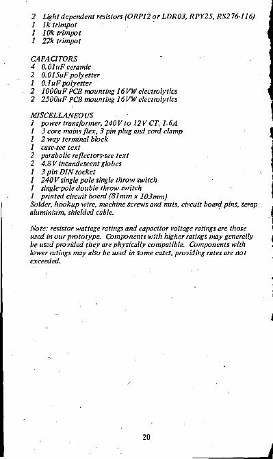
2 Light dependent resistors (ORPJ2 or LDR03, RPY25, RS276-116} 1 1 k trimpot , 1 JOk trim pot 1 22k trimpo t
CAPACITORS 4 0.0luF ceramic 2 0.0JSuFpolyester 1 0.1 uF polyester 2 1 000uF PCB mounting 16 VW electrolytics 2 2500uF PCB mounting 16 VW e/ectro/ytics
MISCELLANEOUS 1 power transformer, 240V to 12V CT, J.6A 1 3 core mains flex, 3 pin plug and. cord clamp 1 2 way terminal block 1 case-see text 2 parabolic reflectors-see text 2 4.BV incandescent globes 1 3 pin DIN socket 1 240 V single pole single throw switch 1 single-pole double throw switch 1 printed circuit board (81 mm x 103mm} Solder, hookup wire, machine screws and nuts, circuit board pins, scrap aluminium, shielded cable. ,
Note: resistor wattage ratings and capacitor voltage ratings are those used in our prototype. Components with higher ratings may generally be used provided they are physically compatible. Components with lower ratings may also be used in some cases, providing rates are not exceeded.
20
'
J
t I I
I
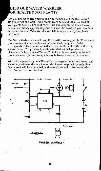
ILD OUR WATER WARBLER OR HEALTHY POT PLANTS
Are you unable to tell when your favourite pot-plant requires water? Do you err on the safe(?) side, water every day, and then find that all your plants have died of root-rot? Or do you only water when the soil has a constituency approaching that of concrete? Now, all your troubles are over. Our new Water Warbler will tell immediately if your plants need water.
The Water Warbler is a small box, fitted with two long prods. When these prods are inserted into soil, a sound is emitted, the pitch of which corresponds to the amount of water present in the·soil. If the soil is dry, a slow 'put-put" is produced, while saturated soil will prod~ce a characteristic high pitched "squeal". Soil that is adequately moist will produce a more pleasant tone, midway between these two extremes.
With a little practice, you will be able to recognise the various tones, and accurately estimate the exact amounts of water required by each plant. Guess-work will be eliminated, and your plants will thrive in soil which is at the correct moisture level.
PRODS 660k • EM401 •
l 251\
A 3
10k 555 .,. 5 5
: 8V
..L
.01
.047
•SEE TEXT
• 5
~ • 1 4
WATER WARBLER
21

1l1e principle behind this useful little device is incredibly simple. The electrical resistance between the two test prods, which depends on tl soil moisture content, is used to control an oscillator, which in turn drives a small speaker. Battery powered, the Water Warbler fits com· fortably in the hand, and will no doubt prove a boon to the home gardener.
Referring now _to the diagram, we can sec that the sole active device is an integrated circuit, the ubiquitous 555 type timer. TI1is is connected up as a nmltivibrator, a1nd drives the small speaker direct. The 0.047uF timing capacitor is charged via the test prods, the 1 k protective resistor, and the !Ok resistor. ·
When the voltage on pin 6 reaches two-thirds of the supply voltage, an internal flip-flop is reset, and pin 7 is grounded. This discharges the capacitor through the !Ok resistor. When the voltage on pin 2 reaches one-third of the supply voltage, the flip-flop is set again, and the cycle starts over again.
Since the· charge rate and the threshold levels are both proportional to the supply voltage, the frequency of operation is independent of supply voltage. This means that the only effect of battery run-down will be to change the intensity of the output. 1liere will be no change in the frequency, so that the Water Warbler will stay "calibrated".
The lk resistor limits the current when the prods are short-circuited, and also sets the maximum rate of oscillation. The 560k resistor sets the minimum rate, and has been chosen so -that a slow "put-put'' is produced. This serves as an indication that the power has been turned on, and should prevent accidental discharge of the battery.
Sound ou:tput is produced by a miniature loudspeaker, of the type that is normally fitted to small portable radios. Since the 555 timer can only supply currents of the order of 200mA, some care is necessary in the choice of speaker impedance. We used a 25 ohm type, and although I this does represent a slight overload, we found it to be satisfactory. 1
Higher impedance speakers can be used without any circuit changes, ~ although the sound output produced may not be as great. Lower impedance speakers can be used with a series resistor, to increase to load on the 555 to an acceptable figure. Thus, if a 15 ohm speaker was used, it would be· necessary to insert a 10 or 12 ohm resistor in series.
1l1e EM401 diode connected across the speaker is to prevent damage to the 555 by any inductive spikes generated by the speaker.
Construction of the Water Warbler should present no difficulties. We used a readily available plastic box as the case. Drill a neat pattern of holes in the front, to act as a baffle for the speaker. This can be held in place using small screws, nuts and washers, placed around the circum
, ference.
22

f
We made our prods from two steel skewers, which we soldered into the ends of brass spacers. This enabled them to be simply screwed to the case from the inside. Connections to the prods were made using solder lugs. The on-off switch can be held in place by self-tapping screws.
We assembled the electronics on a small piece of 2.54mm spacing Veroboard, as this suits the pin spacing of the IC. As the circuit is very simple, we have not provided details of the actual placing of the components. An idea of our layout can be gained from the photographs. Connections to the various elements not on the Vero board can be made using twisted pairs of hook-up wire.
The 560k resistor is most conveniently fitted directly across the solder lugs used to connect to the prods. The Veroboard is supported on a spacer fitted to the screw which mounts the speaker. A short piece of threaded shaft is screwed into the spacer, the Veroboard fitted, and a second screwed spacer fitted. The length of this spacer is adjusted so that it forms a support for the back panel, which is held on with a single screw.
The type of battery holder will depend on the cas~ used.
Use of the device is extremely easy. Simply approach the required pot (stealthily if the plant is sensitive!), switch on, and thrust the prods deep into the soil surrounding the roots. If a high pitched squeal is emitted, then the soil is saturated, and water is definitely not needed.
On the other hand, if the pitch of the sound does not rise on contact with the soil, then your plant is direly in need of water, which should be supplied forthwith. After the water has had time to soak in, test again. If a mellow no.le is obtained, all is well, and your plant will be sure to thrive.
To conclude, a note on safety. The Water Warbler is capable of emitting extremely high pitched sounds, which may affect people with sensitive hearing, as well as dogs and other animals.
PARTS LIST
I miniature speaker, 25 ohms. I switch, single pole single throw. I 555 timer. · I EM401 diode. I I le, I I Ok, I 560 resistors. I 0.0luF, I 0.047uFplastic c11pacitor~ I case. . 4 penlight cells, holder and connection clip. I piece 2.54mm Veroboard. 2 prods, 150mm long.
MISCELLANEOUS Hookup wire, solder, solder lugs, machine screws, nuts, washers, threaded spacers, foam ~bber.
23
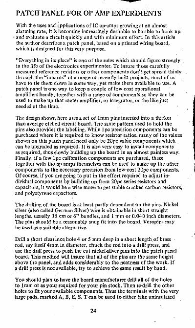
PATCH PANEL FOR OP M1P EXPERIMENTS
With the uses and ;pplications of IC op-amps growing at an almost alarming rate, it is becoming increasingly desirable to be able to hook up and evaluate a circuit quickly and with minimum effort. In this article the author describes a patch panel, based on a printed wiring board, which is designed for this very purpose.
"Everything in its place" is one of the rules which should figure strongly in the life of the electronics experimenter. To insure those carefully ' measured reference resistors or other components don't get spread thinly through the "innards" of a range of recently built projects, most of us have to tie them down in some way, yet make them available to use. A patch panel is one way to keep a couple of low cost operational amplifiers handy, together with a range of components so they can be used to make up that meter amplifier, or integrator, or the like just needed at the time.
The design shown here uses a set of Imm pins inserted into a thicker than average etched circuit board. The same pattern used to hold the pins also provides the labelling. While !pc precision components can be purchased where it is required to know resistor ratios, many of the values shown on this patch panel need only be 20pe value components which can be upgraded as required. It is also very easy to install components as required, thus slowly building up the board in an almost painless way. Finally, ifa few !pc calibration components are purchased, these together with the op amps themselves can be used to make up the other components to the necessary precision from low-cost 20pc components. Of course, if you are going to put in the effort required to adjust individual components by building up from 20pc series resistors and capacitors, it would be a wise move to get stable cracked carbon resistors, and polystyrene capacitors.
The drilling of the board is at least partly dependent on the pins. Nickel silver (also called German Silver) wire is obtainable in short straight lengths, usually 15 cm or 6" bundles, and I mm or 0.040 inch diameters. The pins should be a reasonably snug fit into the board. Veropins may be used as a suitable alternative.
Drill a short clearance_ hole 4 or 5 mm deep in a short length.of brass rod, say itself 4mm in diameter, chuck the rod into a drill press, and use the drill press to push the cut nickel-silver pins into the patch panel board. This method will insure that all of the pins are the same height above the panel, and adds considerably to the neatness of the work. If a drill press is not available, try to achieve the same result by hand.
You should plan to have the board manufacturer drill all of the holes to Imm or as your required for your pin stock. Then re-drill the other holes to fit your available components. Thus the terminals with the very large pads, marked A, B, E, S. T can be used to either take uninsulated
24 l
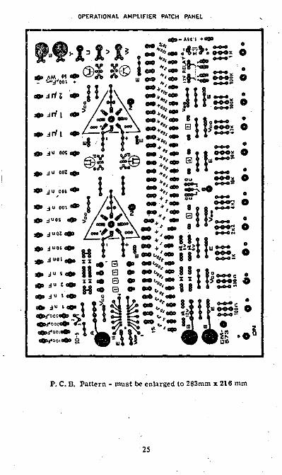
OPERATIONAL AMPLIFIER PATCH PANEL
P. C. B. Pattern• must be enlarged to 283mm x 216 mm
25
metal terminals, or the Philips type of terminals with insulated knobs, but removable base insulators. No soldering will be required for these. A different type of terminal might be used at "V" and "W''. The potentiometers at the bottom of the panel are spaced for the 22 mm diameter miniature carbon pots, but any others which fit will do. These have bushings which require 9/32 inch drills for their clearance holes. The off-on switch at the lower left, and the push switch marked Sat the centre, are for¼" bushing switches. The two positions just below the op ~mp triangles are the nulling SK potentiometers, which may be screwdriver adjust types which fit a ¼" panel hole, or another pair of miniature pots which require slightly larger holes:
Capacitors, resistors, FET's, and transistors are all slung from their leads beneath the panel. This means that there should be a box for supporting the patch panel, so you might as well plan to make room for the required power supplies (which might be two 12V batteries) cord stowage, a place to put your patch leads, extra components, and so forth.
The few other components which should be mentioned are: (I) the 12V relay, which may be used for some experiments with integrators to make up a voltage to frequency converter with !pc accuracy.
Item (2) is the pair of sockets for the op amps. You could use Ferranti S8 sockets with the pins bent out, as we did, or surface mounting sockets, or just solder the op amps directly to the boards.
Item (3) would be diodes, and any general purpose silicon diodes would do very well. For the bridge it would be best to select four matched diodes from a batch. This is easily done with an ohmmeter. Any four diodes which have the same apparent forward resistance are OK.
Item (4) would be the zeners. Again, here it would be a good idea to match them carefully to some nominal 6 or 12V rating, then write down what you've measured at that time and stick it somewhere on the panel. All diodes are mounted below the panel with their leads up through the centre of the rows of three holes. This leaves room for two connector pins for every terminal.
The transistors and JFETS's make up items (5) and (6). Again, selected units as similar as possible, or those which the manufacturer assures you are complementary NPN and PNP, P-channel (top JFET) and N-channel (bottom JFET). The transistors should have betas within about 20pc or better of one another, and be able to handle 200 mA in saturation with voltage ratings at least the full power supply voltage, say 30V for + 15V supplies.
The final items of note would be the accessory sockets for the 16-pin DIL package devices and the TO-5 socket. Not all available sockets can be mounted on top of the panel, so make it possible to swing the panel up to stick in what you need into these sockets from below. The spaces which are numbered I through 7 in boxes are spare spaces for whatever you wish.
26 I
The Patch Panel is designed around the garden-variety 741 fully protected op amp with its own compensation. Any others can be used of course, provided they will fit in the 8 pin T0-99 size can, but you may have to iearrange the wiring for other units.
The real heart of such a patch panel is its op amps, but the veins and arteries are the patch cords. You can use those made by Limrose Electronics in England. We have made up. our own using cup connectors. Cords of 75, 125, 175 and 250 mm length are required for most lay• outs, at least 3 of each with a few extra of the shorter lengths. A bit of heat shrinkable tubing makes a nice finish on these connectors.
For the experimenter who must save every penny, just break apart some old nova! valve sockets and use the bare pin co·nnectors from these. Again a bit of heat shrinkable tubing permits one to get a grip on the connector and not the wire.
Although no power supply has been described for this unit, the "Simple Dual Power Supply for Op Amps" described in Ba bani Press book no. 217 should prove satisfactory. Power supply components can be mounted inside the chassis used to support the patch panel.
That's it! Your patch panel can be as complete as possible, or as complete as you require it to be. It can use junkbox parts which have been assembled to the required precision, or off-the-shelf high precision components, or perhaps just components you have around which do the job. In any case the parts will stay put where you can find them, and will soon be known in value. They, like old friends, will be there when you need 'em, and can be relied on to be consistent if not perfect. Good op amping!
27
CRYSTAL LOCKED MUSICAL TONE GENERATOR
Here's a project that should, once and for all, resolve the uncertainties of musical pitch. Though presented here as a tuning
0
standard, with every note under firm crystal control it offers the potential of crystal locking existing organs, as well as being a possible tone source for synthesisers and computer-controlled mus"ic generators.
Primarily, the aim of the present project is to simplify the problem which faces enthusiasts and musicians of tuning their instruments In a precise and uniform manner. Perhaps a 1ittle background would be helpful.
Before the era of electronic instruments, tuning pianos and organs in particular was regarded as something of an art, understood and practised by relatively few people. It involved setting the frequency of a single note with the aid of a tuning fork or pitch pipe, then setting up one complete basic•octave, by playing pairs of notes in a particular sequence and reacting to the beats between them.
The basic adjustment would then be extended over the whole keyboard, till the necessarily noisy job was finished.
However, over the past 25 years or so, the realm of music making has been invaded by scientists and engineers - short on mystique but strong , on mathematics! They pinned down the formerly errant musical pitch to a precise A = 440Hz. Then, by dividing the octave of the tertlpered scale into its 12 precise intervals, they nominated the frequency of each semitone correct to several decimal places.
Against this background, the job of tuning electronic instruments at least should have become merely a matter of turning a knob or reading a meter but, at a practical level, it hasn't been as easy as this.
The technology behind audio gene;ators, frequency meters and such like, while more than adequate for amplifier testing, has lacked the precision necessary to set the intervals of the musical scale. Even those instruments especially designed as electronic tuning aids have tended to rely on extrapolation from a single reference somewhere within their range. They have lacked the assurance that every single interval was individually and permanently locked to a reliable standard.
One possibility that was considered some years ago was to have a set of precision crystals, in a semitone relationship, with a divider chain capable of reducing the selected crystal frequency to the corresponding musical pitch. But, for most enthusiasts, it was fated never to be more than a possibility, because of the cost of the crystals required.
28
.., "'
Below is a block diagram showing the basic circuit configuration. A master tone generator outputs twelve semitones to a divider chain capable of dividing each semeitone by up to eight octaves. Above is the completed prototype.
2MHi OSCILLATOR
~g1:~+• ----1 FILTER
POWER AMPLIFIER
/
·~ ·o· l . .
-Ej "IJ . .
~ -01 t;
• ! .
30 I
I
With the evolution of more sophisticated divider circuitry, it became feasible to envisage a single, stable high frequency oscillator and divider chains set up for selected whole numbers, which would divide the one source frequency to audio tones closely approximating semitone intervals.
Calculation showed that a very convenient frequency for a master oscillator would be 1.999360MHz - a frequency for which good quality crystals can be ground relatively cheaply. This can be divided down to frequencies suitable for the top octave of a typical instrument by a series of whole numbers, as follows: C, 239; B, 253; A sharp, 268; A, 284; G sharp, 301; G, 319; F sharp, 338; F, 358; E, 379; D sharp, 402; D, 426; C sharp, 451.
While an intriguing possibility, it posed the very practical problem, initially, of requiring far too many discrete components to be the basis of a "handy" tuning aid.
Faced with this, we looked at the alternative, several years ago, of using a single divider chain, but switching the logic circuitry to produce one semitone at a time, as required. But the problem then became one of wiring complexity, along with the cost of the necessary switch.
More recently, the designers of integrated circuits have addressed themselves to the problem, prompted in particular by the demands of electronic organ manufacturers. Logic circuits involving large ·numbers of active components and interconnections have progressively been compacted until they have now been squeezed into a. single integrated chip!
And this forms the basis of our new tuning standard."
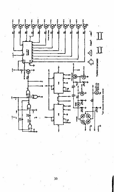
A single crystal oscillator provides a highly stable output at 1.999360MHz (or 2MHz - this involves an error of only 0.03pc). This deives the logic IC, which delivers twelve simultaneous outputs, each representing a semitone in an octave at the very top of the musical scale. By means of a simple switch, any one of these semitones can be fed to a divider chain which makes that semitone available in any octave right down to the bottom of the register. A second simple switch allows any one to be selected and fed to a loudspeaker or an external CRO circuit ..
In short, the tuner can provide any required semitone in any required octave - each one of them directly and precisely controlled by the master crystal. The precise "handy" electronic tuning aid has become a reality, thanks to modern IC technology.
The device which actually triggered the development of the instrument is the A Y-1-0212, made by General Instrument Microelectronics Ltd. This is a MOS large-scale JC which comprises twelve separate divider chains, one for each note, all on a chip mounted in a normal 16-pin dual in-line package. The device will operate from input frequencies anywhere between I00kHz and 2.5MHz, and can thus be arranged to produce its twelve output frequencies at a variety of pitches, if required.
31
As soon as we learned of the availability of this device, we obtained samples and immediately set about the development of the basic tone generator module which forms the heart of the present instrument. However just as we were finalising the module design, we learned that another IC of this type had also become available.
The second device Is from the Mostek Corporation, of Texas, and is designated the MKS0242.
Needless to say, we obtained samples of this device just as soon as we could, and compared it with the AY·l-0212 device, around which we had designed the module. Happily, we found that although the two are not quite identical, they are so nearly so that the MKS0242 may be used in the module with only minor changes. Hence we are recommending the two devices as equally suitable alternatives. Primarily this means that readers should have twice the chance of being able to buy the key tone generator IC, than if only one of the devices were available.
Before we look at the circuit, it should perhaps be explained that there is a certain amount of flexibility about choosing the crystal frequency.
As we noted earlier, the division ratios used to produce the twelve notes are whole numbers in the range 239 to 451. As one might expect, these are a practical compromise; they must be made no larger than is neces• sary to produce acceptable accuracy within the octave, in order to keep the complexity of the IC pattern within reasonable bounds. Naturally because of this compromise the actual note frequencies produced are not separated by the exact twelfth-root-of-two intervals defined in the true tempered scale, although they are quite close enough for almost all , normal musical purposes.
The largest actual error is something like 0.1 !pc. In practical terms the only significance this has is that if one chooses the crystal frequency to make say "A" exactly correct at 440Hz and its multiples, then all of the other notes - including "C".:.. will have a slight error in terms of absolute pitch. On the other hand it is possible to choose a different crystal frequency such that "C" and its multiples have exactly their correct absolute pitch, although this will obviously make "A" and the other notes slightly out.
Thus the crystal frequency which is strictly needed to make "A" exact,ly right turns out to be 1.999360MHz, the figure noted earlier, while that needed to make "C" exactly right is slightly higher at 2.00091 I MHz.
As you can see, these frequencies are very close together. One is only 0.032pc lower than 2MHz, while the other is only 0.045pc higher than 2MHz, These errors are half an order cif magnitude smaller than the errors in the basic scale, so that from a practical point of view we are really splitting hairs.
32 I
rr you have a particular reason for wanting absolute pitch accuracy, then this compromise crystal frequency may not be good enough. In that case you will merely have to obtain a crystal to order on one of the more exact frequencies given above.
At the heart of the present instrument, then, is one or other of the tone generator ICs, together with a crystal oscillator operating at a nominal 2MHz. The oscillator uses thred of the gates from a low cost 7 400 ITL device. Together with these we have added twelve buffer stages for the basic note outputs, using discrete transistors. We have \ also added two binary divider stages, using 7493 ICs. These provide four division flip-flops each, so that together they make it possible to lower the note selected by up to eight octaves.
We have combined this basic circuitry with a simple power supply, to produce a complete self-contained music generator module which may ultimately be used for other projects besides the present tuning instru• men!. The module is based on a printed wiring board which measures 125 by 168mm
To form the tuning instrument, all that is needed apart from the board module is a small stepdown transformer, two rotary switches to select the note and the pitch required, and a simple loudspeaker driver circuit.
The board is basically designed to be used with a standard 0.150 inch printed circuit board edge connector )laving 32 contacts. However, we have made provision for the use of circuit board pins and directly soldered on leads. We made our prototype using the edge connector, as this made frequent removal and replacement quite easy.
The AY-1-0212 device requires supply voltages of +12V plus or minus lV to pin 1, OV to pin 10 and -15.5V plus or minus 1.5V to pin 9. Pin 2 is the input connection, and the twelve outputs are available from , the remaining pins.
The printed circuit board was designed to supply these voltages to the AY-1-0212, using three separate zener diode referenced supplies working from a transformer with two 12V secondaries.
The MK50242 only requires a single supply rail. The recommended supply voltage ranges from +UV to +16V, with a typical value being +15V. It is thus possible to use the same +12V supply as required by the AY-1-0212. The components required for the-15.5V supply can be left off the board as they are not needed, giving a small saving in cost. This is partially offset by the increased price of the MK50242 as compared with the AY-1--0212. ·
33
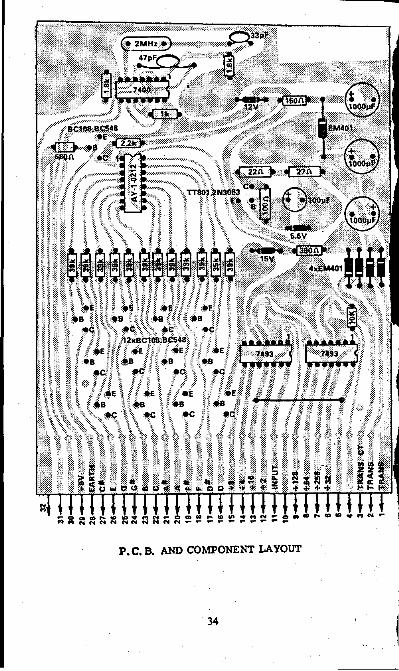
P.C.B. AND COMPONENT LAYOUT
34
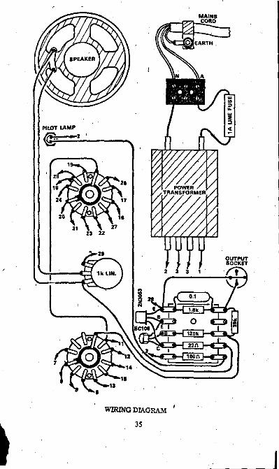
PILOT LAMP
@:::::·=.:2_'--.....
WIRING DIAGRAM
35

The crystal oscillator circuit is basically the same as in the 200MHz counter. This consists of a 7400 quad gate wired in the manner recommended. We have used the fourth gate to provide a buffered auxiliary output, so that if required the 2MHz output would be avail-
, able for use with any other equipment.
Provisiofl has been made on the printed board for a trimmer capacitor to adjust the frequency of the crystal oscillator. However this will not normally be required in the present application. In place of the trimmer and its shunt capacitor, the circuit should normally be wired with a single 33pF NPO ceramic capacitor in series with the crystal, as shown in the circuit.
The connection between the crystal oscillator output and the input circuitry of the tone generator IC is made via a small copper link, both ends of which are brought out. If an alternative 2MHz signal is available, then this link can be broken, and the signal fed in through the relevant connection., If, after breaking this link, it is required intact once more, then provision has been made to use a wire strap to bridge the gap. -
The input circuitry to the tone generator IC consists of an impedance -and voltage matching stage consisting of a single transistor, working in the common emitter mode. The main function of this stage is to increase the signal level to that required by the MOS device.
Each of the twelve outputs of the IC need to be converted back down to a suitable level for inputing to the TTL dividers. Because of the risk of damage to the IC, it was decided to use twelve separate buffer stages followed by the selector switch, rather than using one stage after the switch. However, since only one output is required at any one time, we were able to use a common collector resistor.
As all these stages are working at less than l0kHz, no special transistors are required. Almost any general purpose audio or switching transistor will be satisfactory, provided that the gain is high enough. The twelve base resistors required need only be¼ watt types.
A twelve-position single-pole rotary switch is used to select which note is to be fed to the dividers. We used a make before break type which we modified by removing the spindle stop, allowing the shaft to rotate completely. This allows easier selection of the notes.
From the note selection switch, the signal passes to the dividing chain, consisting of the two 7493 TTL binary counters wired in series. These give eight octaves of notes additional to those obtained from the tone generator IC, selected by another twelve-position single-pole rotary switch. Only nine of the positions of this switch are actually used, the remainder being left unconnected.
36
The 7493 counters incorporate a reset function controlled by a dual input nand gate. The inputs to ihis gate must be connected to a low logic level before the counter will operate. When they are connected to a high logic level, the counter is reset ..
We have connected both,inputs to the nand gate permanently together, and joined them to a spare output connection, so that the reset function may be used if required. A •mall copper link on the pattern is used to make the connection to ground so that the counter will operate. If it is required to reset the gates, this connection must be broken. Provision has been made to remake the connection with a wire link if required.
A wire link is required to connect the output of the first divider to the input of the second. Both dividers have been arranged so that they may be used inde11endently of each other, if this is required. Provision has also been made for the collector load resistor of the tone generator bu~fer stages to be used with either divider.
These provisions are not particularly relevant in connection with the present project, but are designed with future applications in mind.
As detailed earlier, for the AY•l-0212 we require supply voltages of +12Vand -ISV. A +SV, lS0mA supply is also required to drive the TTL logic, and also to drive the output device. We have used a power transformer having two 12V secondaries connected to form a 24V centre-tapped winding, in conjunction with two back-to-back full wave rectifiers to supply voltages of plus and minus 17V, after filtering by two 1 000µF electrolytic capacitors.
The -lSV supply is obtained using a1400mW zener diode in conjunction
with a series resistor. It is possible to use either a 14, 15 or 16V diode, since the actual voltage is not critical.
To prevent possible interaction between the MOS and TTL logic, the · +12V supply is decoupled from the +SV supply using a diode and another IO00µF electrolytic capacitor. The +12V supply consists of a 400mW zener diode and a series resistor, and is similar to the -lSV supply, except that the diode should be a 12V type. (This supply is more critical than the -lSV line.)
The +SV supply for the TTL logic uses a 5.6V 400mW zener diode in conjunction with a 1 watt general purpose transistor. A IO0µF electrolytic in parallel with the zener diode is used to improve the rippler rejection.
This supply has been brought out to one of the output connectors on the board, so that it can be used to drive the. output devices. Alternatively, if another +SV supply is available, then the relevan't components may be left off the board, and the +SV applied to the connection.
37
Note that if the MK50242 is being used then the -15V supply is not required. The relevant components may simply be left out.
We have provided two distinct output facilities for the tuning instrument. A small speaker serves to give an audible output, so that instruments may be tuned by listening for beat notes. This is driven by a Darlington pair, acting as a switch. This arrangement is very efficient, giving a quite reasonable amount of sound while only drawing 30mA from the +5V supply. It does have the disadvantage that the speaker is being activated by a square wave, but we have not found that this causes any great · difficulty.
The second output facility is a 3-pin DIN socket on the rear of the chassis. The output signal is filtered and attenuated before being· supplied to it, so that the level is suitable for feeding into the auxiliary input of a stereo amplifier, or into the input circuitry of a CRO or similar device.
Before we progre'ss to deal with the construction, a word of warning is perhaps in order concerning MOS devices. MOS devices are susceptible to damage caused by stray electrostatic charges, so that unless reason· able handling precautions ar~ observed, the devices may be rendered inoperative.
To protect the devices during shipment, they are packed in conductive foam. Do not remove your device from its packaging until you are ready to install it in its socket. We will give details of the procedure to be followed in actually installing the device further on in the article. I Construction of the timer is relatively simple, as most of the compon· ents are mounted on the circuit board. Before any components are placed on the board, it should be carefully inspected for any breaks in any of the copper tracks or bridges between them.
Once this has been done, the wire strap can be fitted, followed by the resistors and capacitors.
All¼ watt resistors will fit to the board in the normal horizontal position, but the 1 watt types need to be stood on end. If¼ watt resistors caonot be obtained, then larger types may be used standing up. Take care when mounting the electrolytic capacitors that their polarity is correct, as shown on the printed board overlay.
The power supply components can now be1 fitted. Ensure that the zener
diodes are fitted with the correct orientation, as shown on the overlay.
The fourteen transistors are best fitted next. Do not apply excessive heat as this may d.hnage them.
I
,. I
The socket for the tone generator IC Is the next component to be fitted. When fitting the three TTL IC's; take particular care that they' are fitted with the correct orientation, and in the correct place. Use a hot iron with a small tip, and only solder in those pins which are connected into the circuit.
We have left room on the board for the use of a socket for the crystal, but this is not essential. We did not use one, but soldered the crystal direct to the board.
Carefully check the completed board for any errors, particularly with regard to polarity and position.
The only remaining component to be fitted is the tone generator IC. Particular care is required, as this can be damaged by stray electrostatic charges. Hold the IC by the top, and do not touch the pins. Insert it into the socket by pushing firmly, taking care that none of the pins are bent, and that each one enters its correct socket clip.
The board is now complete, and can be put aside until the remaining construction has been f"mished.
The amplifier for the speaker and the f"tlter and ~ttenuator for the output socket can now be assembled on the tag strip, according to the layout. Also included on this tag strip is the dropping resistor for the pilot light.
Cut the shafts of the switches and the,volume control potentiometer to a suitable length, and fit them to the front of the chassis. If desired, the note selection switch can be carefully disassembled and the stop filed off. This will enable the shaft to rotate through 360 degrees completely, making use of the tuner slightly easier.
The remaining components, including the insulated spacers used to mount the board can now be fitted, using the wiring diagram as a guide.
The speaker is held behind its cutout by four machine screws counter- . sunk into the panel in conjunction with washers and nuts. The screws must be countersunk so that the front panel can be fitted.
We recommend that the wiring between the edge connector and the switches be done using multicoloured wires, as this makes the job much easier and less prone to mistakes. Commence by connecting all the necessary wires to the edge connector.
Once this has been done, position the connector in the approximate position that it will occupy when connected to the printed board, and commence the wiring to the switches. This will have to be done as shown on the Wiring diagram. It will be found that the wires from the connector can be grouped in two major bundles, one to each switch.
39

After ·completion, check thoroughly that no mistakes have been made. When this has been done, the remaining wiring can be completed.
The printed board can now be screwed to its mounting spacers, and the edge connector pushed firmly home. The tuner is now ready for testing. Plug the mains cord into a suitable receptacle, and switch on. The pilot light should immediately glow. Advance the volume control and listen for a note.
If no sound can be heard, rotate the octave switch: i.e. the right-hand · switch. Check that the notes increase in frequency as the switch is rotated clockwise, and that there are no positions where no sound can be obtained apart from the three at either end of the range:
Set the octave switch to the central position. Rotate the note selection switch and check that twelve separate notes can be heard, and that they increase in pitch as the switch is advanced clockwise. If any notes are out of order, check that all connections to the switches are correct.
The front panel can now be fitted. It is held in place by the mounting nuts for the switches and the potentiometer, as well as the pilot light. When fitting the knobs to the switches, ensure that their relative position is correct. The octave switch knob is fitted so that the pointer is vertical when the switch is set to the central octave.
The note selection switch should be positioned so that A= 440Hz can be heard when the pointer is vertically upward. If you are unable to tell this note by ear, set the knob so that the change-over between C and C sharp occurs at the correct place. (These notes are nearly an octave apart, and occupy adjacent switch positions.)
The instrument should now be ready for use.
List of Component Parts
I Case, 230 x 215 x 90mm, with matching front panel J Power transformer, 240V to 12V and 12V at 0.8A .1 Wiring board (125 x I 67mm) 2 Rotary switches, 12-position single-pole I 2MHz quartz crystal, AT-cut fundamental I 70mm dia, JS ohm speaker' I I 6-pin DIL integrated circuit socket J 32-way 0.150 inch pitch edge connector J 6V pilot light J 3-pin DIN socket J I k linear potentiometer J Miniature tag board, 5 prs. tag J Mains cord, plug, rubb_er grommet and clamp 1 JA fuse and in-line [ase holder 3 knobs 1 3-terminal block
40 I
SEMICONDUCTORS I Tone generator IC, A Y-1-0212 or MKS0242 {see text) I 7400 quad nand gate or RS276-J801 2 7493 4-bit binary counters . 2 NPN I watt transistors, 2N3053, BFYS0 or RS276-2030 14 NPN 300 milliwatt transistors, BC/08, BC548 or RS276-2009 I 12V, 400mW zenerdiode,BZX79/CJ2or RS276-563/623 I 5.6V, 400mW zenerdiode, BZX79/CSV6 or RS276-561/621 1 15V, 400mW zenerdiode, BZX79/C15 or similar {AY-I-0212 only,
see text). RS276-564/624 3 Silicon diodes, EM401, RS276-1139, IN4006, BY/27. 2 Silicon diodes, EM401 or simflar {AY-1-0212 only)
CAPACITORS 2 J000µF, 25VW electrolytics, printed circuit board types I J000µF, 25VW electrolytic, printed circuit board type ·
{AY-1-0212 only) I J00µF, 12VW electrolytic, printed circuit board type I 0. I µF polyester I 33pF NPO ceramic I 47pF NPO ceramic
RESISTORS {all¼ watt unless r;pecified otherwise) I 22 ohm, I watt I 22ohm I 27 ohm, I watt I JOO ohm, I watt I JS0ohm I IBO ohm, ½watt I 390ohm {AY-l-02J2only) I 680ohm I Jk 3 I.Bk I 2.2k I /Ok 13 39k I .120k
MISCELLANEOUS Rubber feet for case, multicoloured hook-up wire, insulated spacers, machine screws and nuts, washers, self tapping screws.
41
BUILD THIS NOVEL 'LEDS & LADDERS' GAME!
Here is a lo:,v cost pocket-sized electronic game that will test your patience and sense of timing. Seemingly simple, you may find to your dismay that literally hours of practice are required before you can "reach the top".
Our game consists of a small box, fitted with two switches, sixteen small light emitting diodes (LEDs), and an illustrated front paneL The illustration is a schematic drawing of a well, with a ladder reaching from the bottom to the top. The LEDs are arranged on the rungs of the ladder, representing successive foot positions as the ladder is climbed. The topmost LED, which is a different colour to the other ones, is on the ground at the top of the well. '
When the POWER switch is pressed, the bottom LED commences to flash at a two second rate. The object of the game is simply to make the LED climb the ladder, by appropriate manipulation of the CLIMB button. Success is signified when the different coloured LED at the top is illuminated.
\ The trick in the game is that the CLIMB switch can only be operated when a LED is on. When this condition is satisfied the LEDs illuminate in turn, to simulate the effect of a light climbing the ladder.
If, however, the CLIMB switch is pressed when no LED is illuminated, the player is surprised and infuriated to find that when a LED comes on again, he is back at the bottom of the well. Of course, the device is scrupulously fair, so that even if the switch is only pressed for the shortest of times,, back to the bottom he goes! '
So, having limbered up his wits, as well as his switch operating finger, our player attacks the infernal machine again. With his eye glued to that first LED, and his finger poised, he waits for that light to come on. F1ash!, the LED emits, his finger stabs the button, and the LED com· mences to climb!
One! two! three! four LEDs emit in \urn, the button is released, and a fraction of a second later, the LED goes out. With bated breath, our player scans the LEDs, and is rewarded by seeing the fourth LED come on again. Once more he·stabs at the button, once again the LED com· mences to climb.
Some time later, the fifteenth LED casts a ruddy glow over the perspiring face of our player, who decides to stop for a short time to wipe his brow. Those last few steps had seemed to be harder to climb than the earlier ones, in fact, he'd only just managed to go from the fourteenth to the fifteenth rung in one go. ·
42
E ,. ~ ,. ~ ~ ,<I ~ ,; ~ ,;;:~ ,;.~ "~ ~ ~ I
, ,<' \ ~· ·~ ) <'
"- '- "' '- '- '- '-
[<' ~-=~- ~~ '
~ ~ ,< - '- .... ..
i [:- - . . ·- / -. ~
~ ~ .
, -~
! ~ • ~ :
~ u-. ... i
f{:19 ! . . . '
;,;:,. ~ ~'?c h ·~
: . . ! r.-.
~ ~ H,~ . ;;; !
--J
. .,. ~
0 < ~
' .
:! -. 7 . .
. ' ~ ~ :i
@; ·: · "'
' 9.\
7•-·-· I• !
+ ~
43
u
·El
1·
:~ ·o· ~ ...
·o· . . .
VJ a: w 0 s 0
~ VJ 0 ~
Directing his attention back to the game, our hero is horrified to find that he's slipping back down the ladder, now only the fourteenth LED is alight. Desperately, he punches mindlessly at the button, the LED climbs up higher, just reaches the top, and then goes out. And he's still pressing the switch!
With a heart·rending groan, he releases it, and then watches dejecfedly as the lowest LED flashes merrily. Some minutes later, he musters his courage, and once more commences to climb.
Just in case you're wondering whether or not it is possibl~ to reach the top, we can assure you that it is. In fact the little man at the top is waving to show you that he managed it, so don't lose heart and give up.
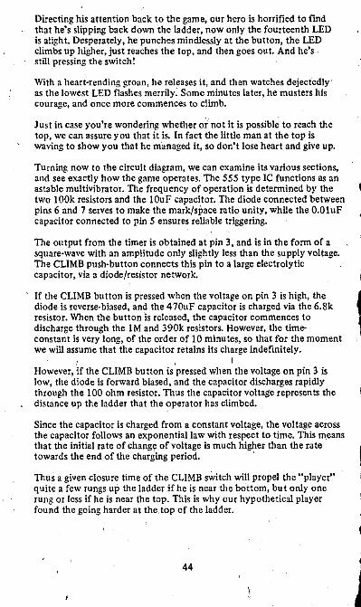
Turning now to the circuit diagram, we can examine its various sections, and see exactly how the game operates. The 555 type IC functions as an astable multivibrator. The frequency of operation is determined by the two 100k resistors and the l0uF capacitor. The diode connected between pins 6 and 7 serves to make the mark/space ratio unity, while the 0.0luF capacitor connected to pin 5 ensures reliable triggering.
The output from the timer is obtained at pin 3, and is in the form of a square-wave with an amplitude only slightly less than the supply voltage. The CLIMB push-button connects this pin to a large electrolytic capacitor, via a diode/resistor network.
If the CLIMB button is pressed when the voltage on pin 3 is high, the diode is reverse-biased, and the 4 70uF capacitor is charged via the 6.8k resistor. When the button is released, the capacitor commences to discharge through the lM and 390k resistors. However, the timeconstant is very long, of the order of 10 minutes, so that for the moment we will assume that the capacitor retains its charge indefinitely.
1 , I However, if the CLIMB button is pressed when the voltage on pin 3 is low, the diode is forward biased, and the capacitor discharges rapidly through the 100 ohm resistor. Thus the capacitor voltage represents the distance up the ladder that the operator has climbed.
Since the capacitor is charged from a constant voltage, the voltage across the capacitor follows an exponential law with respect to time. This m_eans that the initial rate of change of voltage is much higher than the rate towards the end of the charging period. ·
Thus a given closure time of the CLIMB switch will propel the "player" quite a few rungs up the ladder if he is near the bottom, but only one rung or less if he is near the top. This is why our hypothetical player found the going harder at the, top of the ladder.
44
A second feature arising from this exponential curve is that the rate of discharge is greatest at the top of the ladder, so that an error in timing there produces a greater fall down the ladder than a corresponding mistake at the bottom. Now you can begin to see why the game is so infuriating.
The power switch is placed in the negative supply line, and is a changeover type. This is so it can be used to discharge the 470uF capacitor, through a 10 ohm limiting resistor, when the power is turned off.
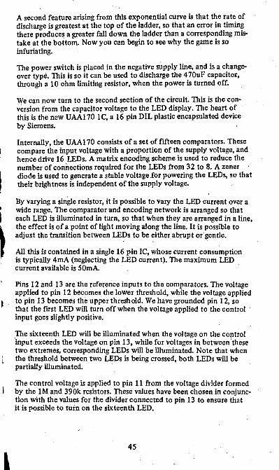
We can now turn to the second section of the circuit. This is the conversion from the capacitor voltage to the LED display. The heart of this is the new UAAl 70 lC, a 16 pin DIL plastic encapsulated device by Siemens.
Internally, the UAAl 70 consists of a set of fifteen comparators. These compare the input voltage with a proportion of the supply voltage, and hence drive 16 LEDs. A matrix encoding scheme is used to reduce the number of connections required for the LEDs from 32 to 8. A zener diode is used to generate a stable voltage for powering the LEDs, so that their brightness is independent of the supply voltage.
By varying a single resistor, it is possible to vary the LED current over a wide range. The comparatorand encoding network is arranged so that each LED is illuminated in turn, so that when they are arranged in a line, the effect is of a point of light moving along the line. It is possible to adjust the transition between LEDs to be either abrupt or·gentle.
All this is contained in a single 16 pin IC, whose current consumption is typically 4mA (neglecting the LED current). The maximum LED current available is SOmA.
Pins 12 and 13 are the reference inputs to the comparators. The voltage applied to pin 12 becomes the lower threshold, while the voltage applied to pin 13 becomes the upper threshold. We have grounded pin 12, so that the first LED will turn off when the voltage applied to the control input goes slightly positive.
The sixteenth LED will be illuminated when the voltage on the control ·input exceeds the voltage on pin 13, while for voltages in between'these two extremes, corresponding LEDs will be illuminated. Note that when the threshold between two LEDs is being crossed, both LEDs will be partially illuminated.
The control voltage is applied to pin 11 from the voltage divider formed by the IM and 390k resistors. These values have been chosen in conjunction with the values for the divider connected to pin 13 to ensure that it is possible to turn on the sixteenth LED.
45
Although we stated earlier that the loading on the 4 70uF capacitor was negligible, this is not strictly so. The lM and 390k resistors, in conjunction with the impedance presented by pin 11, as well as the leakage resistance of the electrolytic itself, combine to,slowly discharge the, capacitor. This discharge is most noticeable when the capacitor is highly charged, and accounts for the "slipping back" observed by our hypothetical player. This effect adds to the difficulty of the game.
The stabilised LED driving voltage is made available at pin 14, and is normally connected to pin 16 by a suitable resistor. We have included a transistor in series wfth a 10k resistor, and used the output of the 555 to switch the transistor on and off. This pulses the LEDs, eliminating the need for a separate flashing indicator.
As well as being economical in terms of components, this also means that a stabilised supply is not necessary. This is because the 555 and the UAAl 70 both use fractions of the supply voltage as their references, making frequency and comparator switching levels independent of supply variations. As the LEDs are driven from a constant voltage source, their intensity does not change with supply voltage either.
We have used eight 1.5V penlight cells to power the circuit, giving a nominal 12V supply. The batteries are mounted in two 4-way holders. The average current drain of the complete circuit is about 25mA, giving an estimated .life of 40 hours.
If required, it would be possible to fit a small transformer and rectifier/ filter assembly in place of the batteries;although the initial cost would be much higher, The voltage applied to the circuit must be kept below 16V, to prevent damage to the ICs.
46
j ~ i
!
a
l
12V I -71 ON-!-. s1 • I
I
TO LEOS
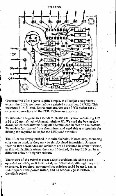
Construction of the game is quite simple, as all major components except the LEDs are mounted on a printed circuit board (PCB). This measures 71 x 71 mm. We recommend the use of PCB stakes for all external connections to the PCB. Fifteen are required.
We mounted the game in a standard plastic utility box, measuring 159 x 96 x 50 mm, fitted with an aluminium lid. We used the box upside down, which necessitated filing off the moulded-in feet on the bottom. We made a front panel from aluminium, and used this as a template for drilling the required holes _for the LEDs and switches.
The LEDs are simply pushed into suitable holes. If necessary, mounting clips can be used, or they may be simply glued in position. Arrange them so that the anodes and cathodes are all oriented in similar fashion, as this will facilitate wiring them up. If desired, the top LED can be a different colour, to signify success. .r
The choice of the switches poses a slight problem. Matching pushoperated switches, such as we used, are obtainable, although they are expensive. If required, non-matching switches could be used, e.g., a slider type for the power switch, and an economy push-button for the climb switch.
47
The completed circuit board is fastened to the lid of the box using machine screws and nuts. The batteries are held in position with a small clamp fashioned from aluminium.
The wiring from the PCB to the LEDs and switches is best done with rainbow cable, as this makes for easy identification of the different leads. Complete the interconnections between the LEDs first, using the circuit diagram as a guide, and then connect them to the PCB.
Construction is then complete and you can attempt to climb the ladder. If the LEDs do not come on in order it is likely that the connections to them are in error. Any LEDs failing to emit will probably have anode and cathode transposed.
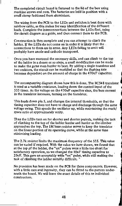
Once you have mastered the necessary skills, and can climb to the top of the ladder in a dozen or so steps, a small modification can be made to make the game even harder to beat. By adding a single transistor and two resistors, the circuit can be modified so that the flashing rate becomes dependent on the amount of charge in the 470uF capacitor.
The accompanying diagram shows how this is done. The BC548 transistor is used as a variable resistance, loading down the control input of the 555 timer. As the voltage on the 4 70uF capacitor rises, the bass current in the transistor increases, turning on the transistor.
This loads down pin 5, and changes the internal thresholds, so that the timing capacitor does not have to charge and discharge through the same voltage swing. This speeds the oscillator up, while maintaining the mark/ space ratio at approximately unity.
Thus the LEDs turn on for shorter and shorter periods, making the task of climbing to the top of the ladder harder and harder as the climber approaches the top. The 1 M base resistor serves to keep the transistor on the linear portion of its operating curve, while at the same time minimising loading.
The 2. 7k resistor limits the maximum frequency of the 555. This value can be varied if required. With the value we have shown, we found that at the top pf the ladder, the "on" pulses were a little too short for· satisfactory operation, so we changed the lOuF timing capacitor to 25uF. This gave an acceptably wide "on" pulse, while still making the task of climbing the ladder suitably difficult. '
No provision has been made on the PCB for these components. However, with a little care and ingenuity, they can be fitted to the pattern underneath the board. We will leave the exact details of this to individual constructors.
48
l
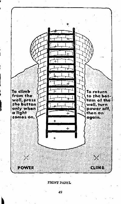
r +
FRONT PANEL
49
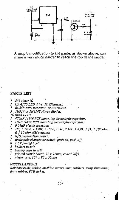
TO EXISTING CIRCUIT
, ,. TO
hlSHNG CIRCUIT
1M
410 16\/W
A simple modification to the game, as shown above, can make it very much harder to reach the top of the ladder.
PARTS LIST
I 555 timer IC I UAAI 70 LED driver IC (Siemens). I BC548 NPN transistor, or equivalent. 3 IN914 or IN4148 silicon diodes. 16 small LEDs. I 4 70uF"J 6 VW PCB mounting electrolytic capacitor. I I 0uF 16 VW PCB mounting electrolytic capacitor. I 0.0luFplastic capacitor. I IM, I 390k, I 150k, 2 I00k, 139k, 2 I Ok, I 6.8k, Ilk, I 100 ohm
& I 10 ohm ¼W resistors. ' I N/O push-button switch. I single pole changeover switch, push-on, push-off. 8 1.5V penlight cells. 2 holders to suit. 2 battery clips to suit. I printed circuit board, 71 x 71mm, coded 76g3. I plastic case, I 59 x 96 x 50mn~
MISCELLANEOUS Rainbow cable, solder, machine screws, nuts, washers, scrap aluminium, foam rubber, PCB stakes.
50
MAGIC' TABLE LAMP USES LOW-COST TOUCH SWITCH .
A touch-controlled switch can be put to a variety of uses. In this article we explain how to make such a device from economical parts, and then show how to incorporate' this into 3.n attractive table lamp.
When I was a boy, I made a table lamp. It was one of my first wood-work proje'cts at school, and was my pride and joy. That was, until the teacher politely asked "How do you turn it off?" I had forgotten the switchand it was almost impossible to fit one to it.
Just lately, I've made another lamp without a switch. At least, that's what,it looks like-until you touch it. Surprise! It comes on. Touch H again, and it goes off.
All this has come about by means of a touch switch - one of those electronic toys which can·be put to a large variety of uses, and not all of them trivial, either. You may have noticed many modern lifts have call buttons which do not need pressing - just touching. Some of the latest generation of colour television receivers similarly have channel selector buttons which are touched to call up the channel. Both these are examples of touch switches in action.
While the examples given are likely to be controlled-by integrated circuits, it is just as easy (and often cheaper)to do the job with discrete components. For example, our touch switch circuit uses garden-variety transistors-we happened to use BC108s, but any small signal NPN transistor would do the job. '
In fact, practically all components in our touch switch could come from a well-stocked junk box. Even if you buy all new components, the touch switch circuitry shouldn't cost a lot.
Before we go any further, we had better explain just how our touch switch works, and variations possible on the original. Actually, while they are called touch switches, most devices of this type are really proximity switches - that is, they work by something coming close to the touch plate ot pad, but not necessarily touching it.
They do this because the body of the person attached to the hand or finger touching (or coming close to) the pad represents quite a large order of capacitance to ground-· even though there is no physical connection between the body and ground.
Turning our attention to the circuit, the first transistor is connected as a Colpitts RF oscillator, with a frequency somewhere around 400-SOOkHz. Actual frequency of operation is unimportant, so long as the frequency doesn't happen to be either 455kHz or above 5 30kHz, which could tend to make radio reception in the near vicinity a little difficult!
SI
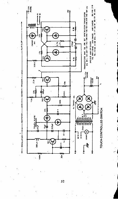
>-.
1 ,. ; •o ' '!~ . gi . .. .. .
===tf ~~
.. . •• :; zO
5! ::: .o . - .. o" 0
' u~ ~~ ~: f~ g~ z,
• I .. ;o -·· o••
0 :; co ... Q::li ~
•-· z>' .. ~ !'
' . .o O• 0
C a ~
>-,, . ±i
~f >
~ 0
:, 0 .~ ~= • .,
i ~ I ~ ~
~
X j u ... . "
~ j <I)
~ . 0
• _j
.. ... ... ' 0
~ a: ... . z 0
0
; .. u
• x
~ u
~ ::,
0 0
l ...
,- ~ • z
~ ~ I j
52 j
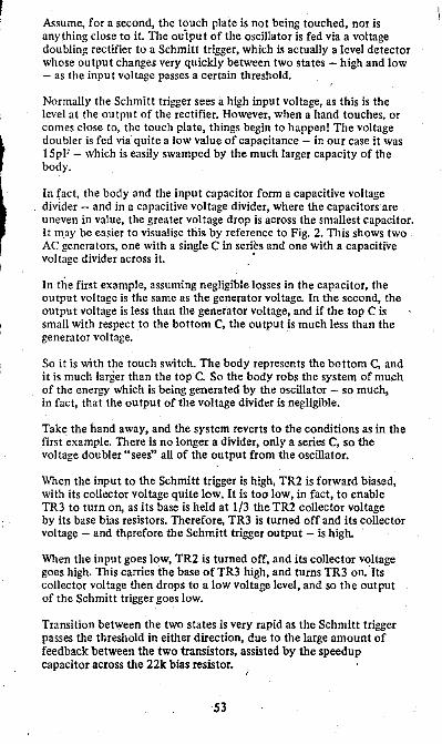
r Assume, for a second, the touch plate is not being touched, nor is anything close to it. The ouiput of the oscillator is fed via a voltage doubling rectifier to a Schmitt trigger, which is actually a level detector whose output changes very quickly between two states - high and low - as the input voltage passes a certain threshold.
Normally the Schmitt trigger sees a high input voltage, as this is the level at the output of the rectifier. However, when a hand touches, or comes close to, the touch plate, things begin to happen! The voltage doubler is fed via quite a low value of capacitance - in our case it was I Sp F - which is easily swamped by the much larger capacity of the body.
In fact, the body and the input capacitor form a capacitive voltage divider - and in a capacitive voltage divider, where the capacitors·are uneven in value, the greater voltage drop is across the smallest capacitor. It m_ay be easier to visualise this by reference to Fig. 2. This shows two AC genera tors, one with a single C in series and one with a capacitive voltage divider across it. ·
In the first example, assuming negligible losses in the capacitor, the output voltage is the same as the generator voltage. In the second, the output voltage is less than the generator voltage, and if the top C is small with respect to the bottom C, the output is much less than the generator voltage. ·
So it is with the touch switch. The body represents the bottom C, and it is much larger than the top C. So the body robs the system of much of the energy which is being generated by the oscillator - so much, in fact, that the output of the voltage divider is negligible.
Take the hand away, and the system reverts to the conditions as in the first 'example. There is no longer a divider, only a series C, so the voltage doubler "sees" all of the output from the oscillator.
When the input to the Schmitt trigger is high, TR2 is forward biased, with its collector voltage quite low. It is too low, in fact, to enable TR3 to turn on, as its base is held at 1/3 the TR2 collector voltage by its base bias resistors. Therefore, TR3 is turned off and its collector voltage - and th~refore the Schmitt trigger output - is high.
When the input goes low, TR2 is turned off, and its collector voltage goes high. This carries the base of TR3 high, and turns TR3 on. Its collector voltage then drops to a low voltage level, artd so the output of the Schmitt trigger goes low.
Transition between the two states is very rapid as the Schmitt trigger passes the threshold in either direction, due to the large amount of feedback between the two transistors, assisted by the speedup capacitor across the 22k bias resistor.
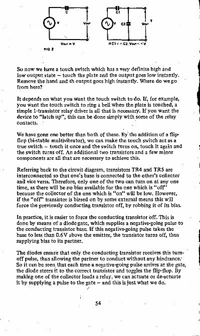
om· Voo.i••V HC1<'"".C2,Y°""<<V
1'10.2
So now we have a touch switch which has a very definite high and low output state - touch the plate and the output goes low instantly. Remove the hand and th output goes high instantly. Where do we go from here?
It depends on what you want the touch switch to do. If, for example, you want the touch switch to ring a bell when the plate is touched, a simple I ·transistor relay driver is all that is necessary. If you want the device to "latch up"; this can be done simply with some of the relay contacts.
We have gone one better than both of these. By' the addition of a flipflop (bi-stable multivibrator), we can make the touch switch act as a true switch - touch it once and the switch turns on, touch it again and the switch turns off. An additional two transistors and a few minor components are all that are necessary to achieve this.
Referring back to the circuit diagram, transistors TR4 and TR5 are interconnected so that one's base is connected to the other's collector ana vice versa. Therefore, only one of the two can turn on at any one time, as there will be no bias available for the one which is "off' because the collector of the one which is "on" will be low. However, if the "off' transistor is biased on by some external means this will force the previously conducting transistor off, by robbing it of its bias.
In practice, it is easier to force the conducting transistor off. ·This is done by means of a diode gate, which supplies a negative-going pulse to the conducting transistor base. If this negative-going pulse takes the base to less than 0.6V above the emitter, the transistor turns off, thus supplying bias to its partner.
The diodes ensure that only the conducting transistor receives this turnoff pulse, thus allowing the partner to conduct without any hindrance: So it can be seen that each time a negative-going pulse arrives at the gate, the diode steers it to the correct transistor and toggles the flip-flop. By making one of the collector loads a relay, we can actuate or de-actuate it by supplying a pulse to the gate - and this is just what we do.
I
54
The Schmitt trigger output is normally high, and when the touch plate is touched, it goes low - that is, it is a negative going pulse. This is fed into the gate and so toggles the flip-flop. If the relay was closed, it now opens - and vice versa. In the interests of reliable triggering, we have made the collector loads equal - a 220 ohm IW resistor matches the resistance of the relay coil. While this might appear wasteful of power, it assists the. flip-flop by making both sides as equal as possible, so one side is not harder to. toggle.
One might ask why use a relay at all - why not some other form of power control device which does not use as much power itself? The answer is safety. The touch.switch is quite suitable for controlling mains loads (and we will say more about this in a moment) but, because you can actually touch the plate which is connected into the circuit, isolation is needed. A relay provides this isolation.
So now we have an on-off touch switch -what will we do with it? One use which immediately sprang to my mind is a touch-control bedlamp. Have you ever woken in the middle of the night with a baby screaming and tried to find that teeny weeny switch to turn the lamp on? (You're not married and have no kids - oh well ... ) How abollt when you want to get up at 4 am and vou knock the lamp over trying to turn it on to see the time.
To make construction of a lamp as easy as possible, we elected to use a ,single length of extruded aluminium tube as the base, plugged each end with a 25mm thick disc of softwood. The electronics are mounted on the bottom disc inside the tube, while a ceiling-type lighting fixture screws to the outside of the top disc thus allowing a lampshade to be fixed.
The aluminium tube should not be too hard to acquire - especially if you have a specialist aluminium centre nearby.
The tube diameter was as large as we could buy - 100mm od, (approx. 93mm id) and approx. 200mm long. Length of the base is really a matter of personal preference, determined to a large extent by the type of lampshade to be fixed to it. If you have access to a lathe, the ends of the tube can be smoothed most easily. If not, a file will do the job, but it will take just a little longer.
The wooden disc "plugs" t?3Y cause a few problems for some readers. Ideally, they should be turned on a lathe for proper fit, but they can be cut using a coping saw and truing them with a rasp. They can also be turned on an electric drill. The bottom disc should be a tight fit - so tight, in fact, it needs to be belted in with a mallet. This is for appearance more than anything else - it saves having to put screw holes in the base of tlie tube where they can be seen.
55
be batten lamp holder / , .
- Top plug .
-' I
I
Aluminium Tube
1 Slot to clear mains lead ' I
:11
0
Bottom plug
56
The top plug can - and should - be a loose fit in the tube, as it is held in by screws which are normally hidden by the shade. If anything does go wrong with the touch switch, it is not too difficult a job to remove the top plug and hammer the bottom one out.
Incidentally, should you have a lathe at your disposal, don't be afraid to drill a hole through the centre of each plug - you will need to any• way, This can be up to about 12mm or so. It is easier to grip the wo,od from the centre using a bolt than to try to grip the outsides.
Once the plugs have been cut to size, the electronics can be fitted. The printed circuit board is attached with two right-angle brackets so it is vertical It is important to maintain at least 5mm spacing between the edge of the PCB and the edge of the base plug - otherwise you risk a short to the metal cylinder. At best, this will stop the switch working; at worst, you will connect 240V to the cylinder. Need we say more?
(Just to be on the safe side, after assembling the PCB I covered all exposed mains connections and tracks with insulation tape before final assembly.)
The connection between the PCB and the metal cylinder, a strip of thin tinplate is used, which should be bent to the correct shape before soldering into place. Also, a channel is cut into the base plug to take this extra thickness. It must be deep enough to allow the base to slide into the tube, but shallow enough to ensure reliable contact between the tinplate ~nd aluminium.
The 'channel can be tapered a little - deepest ai the top, to achieve this aim. The edge of a file can be used as it does not have to be deep. Then the tinplate can be cut slightly narrower than the file to fit in the channel ,
A single panel pin holds the tinplate in place on the base plug - don't rely on a solder joint to hold it. With the tinplate held in place, solder the end to the co:rect point on the back of the PCB.
The next step is to drill a hole through the side of the base for the mains ead to pass through. This can be done from just about any position around the circle, as the associated keyway in the aluminium tube can be drilled later to match it. The hole is drilled· on a radius, about 12 mm up from the underside of the base, and about 6 mm in diameter.
This hole mates with the one mentioned previously, that drilled through the centre of the wooden cylinder to assist turning. The incoming mains cord passes through both these holes, first the horizontal and then up through the vertical one to the "works".
The transformer and mains wiring can now be attended to. A 3 section, mains terminal block holds the incoming mains wires and inter•connec• lions to the transformer - refer to the wiring diagram for full details. A small mains cord clamp holds the lead itself.
57
u, 00
The mains earth lead goes to the transformer case and also to one side of the transformer secondary. This is to try to cut down as much hum L
induction as possible.
Incidentally, some readers may wonder about the latitude allowed in the choice of transformer. On the circuit, we have specified a 6-9V secondary. The reason is that the circuit itself will happily work on supplies from around 6 to 18 or so. The relay, however, needs 8-12V DC to work correctly - and a transformer whose rectified voltage falls within these limits is quite satisfactory.
Remember when wiring the mains section that you are dealing with a device which people touch - your wiring must be exemplary. With Correct wiring, this device is quite safe. But if,you boo--boo ....
The wiring of the light socket is best left until last - both for safety reasons and because the leads should be cut as short as possible for hum induction reasons - and this is n'ot possible until both plugs are in
I· position. The checking operations to be described can be carried out by listening to relay-operation - either a single click for correct operation or "chatter" or no sound for incorrect operation.
Now comes the curly part - matching the switch to the cylinder! Perhaps a word of explanation is in order. Remember how the switch works - capacitor action dividing the voltage when the plate was touched. Unfortunately, this is exactly what the cylinder is - a "body" attached to the touch plate. In fact, this can cause the switch to lock on or off, as it sees a load on its touch plate·at all times.
For_ this reason, a small amount of juggling of the coupling capacitor might be necessary. We found that the value shown, 15pF, was exactly right for our tube - but it may not be right for other lengths of tube. So it must be checked, and the easiest way to do this is to lower the tube onto the base just far enough to contact the tinplate strip, and see if it works when you touch it. If it doesn't work at all, or breaks into "chatter", the value has to change. Go up if it chatters, down if it doesn't work at all.
As a guess, the outside limits would be about l0pF to 25pF. The lower you go, the more sensitive it becomes, but also is more sensitive to hum fields - hence the chatter. And vice-versa, of course. Even with the optimum value of capacitor in our version (chosen by trial and error) we were still able to make the thing chatter by cheating. If the whole
'\ flat of the hand was brought in close to the cylinder and held there, the relay would chatter - but this is not the correct way of using it, so we weren't too concerned. A single touch is all that is n,ecessary.
By the way, if you are not planning on making the touch switch in the lampshade form but wish to use it for some other purpose, it may interest you to know that the lower you make the capacitor the more
59
like a true "proximity detector" it becomes. In fact, with a value of lpF and a small touch plate, it will actuate from at least 20mm away and more. But this only holds where the mains hum field can be kept away.
Once you are sure the switch is working correctly, pull the base out of the tube and connect the "lamp" leads to the terminal block and PCB. Note the relay is in the active side of the line, following normal mains wiring practice. ' I
Now wear~ almost ~eady for final assembly. First of all, a keyway has to be cut in the tube for the mains cord. This can be done with a 6 mm drill, drilled about 10mm from the bottom of the tube. Open it out to a slot with a file, taking care not to mar the appearance.
The three holes to hold the top plug can also be drilled. Divide the circle into three (remember the "flower" pattern you used to draw at school with a compass - this accurately divides a circle into 6 - and so 3), and drill the holes to suit the size of screw you are using. The best type is a countersunk head, nickel plated, around one inch long and a fairly small gauge.
The holes can be drilled about 10mm down from the top of the plug. While you're about it, drill a pilot hole to match the holes in the aluminium - this will assist in final assembly. Remember to use a smaller drill, though! Remove the plug, and countersink the holes as necessary.
Now is the time to place the bottom plug in position. Carefully line up the mains cord keyway and the mains cord emerging from the base, and push the base hard down into the tube. If it is a proper fit, you won't get very far before you have to use a hammer and block of wood to keep it going. Don't belt the base too hard, take it in small "bites" working around the circle. Stop when the base is just proud (1-2mm) of the aluminium. This allows the lamp to rest on wood, rather than on aluminium.
The light fixture can now be screwed to the plug top. If you examine the fixture itself, you will note that the socket can be removed from the base by pushing it out from the front. It can be replaced from the front by turning it so the catches on the socket can pass through the slots in the base. A turn of a few degrees will then place the catches behind their counterpart on the base and the ring can then be screwed on to make it captive. ·
Separate the two halves of the socket, and screw the base into the middle of the top plug. Make sure you are exact here, as any error will appear amplified -,yhen you place a shade on. With the socket firmly on the wood, pull the lamp leads up through the tube and through the hole in the plug. Now push the plug down into the tube so it is 20mm or so down from the top.
60
Pull the lamp leads fairly tight, and cut them off so there is approx. 20mm protruding from the tube. Bare them back 5mm, and screw them into their positions on the socket. A normal socket has three holes -use the two outside ones. Now pull the top plug back up, and loosely fasten it in place with the woodscrews.
Push the socket into position on its base (as just described) noting how much slack there is in the leads. If there is too much, and the leads go too close to the tube, hum troubles may result, as we found. Ideally, the mains leads should pass directly up the ·centre of the tube. If there is too much slack, repeat the last couple of steps until there is as little slack as you can handle. Then screw the ring onto the socket to tighten it up.
If the ring keeps turning and the socket comes out of its base, you haven't turned the socliet so the catches engage. Release the ring and .turn the socket around slightly - then re-tighten. Last of all, do up the screws on the side and the lamp is finished.
As a final check, place an ohm-meter (1) across the lamp socket terminals; (2) between each of the terminals and the barrel of the lamp; (3) between each of the mains plug pins and the barrel of the lamp. If there is a reading between any of these, something is wrong and should be checked before use.
The lampshade is left up to the individual. They may be bought quite readily, or may be made from parts obtained at specialist shops. Either way, choose one which is not too small - it will look odd because of the "chunkiness" of the base - nor one too large, which may promote instability even though the base is quite heavy.
Lamp wattage is as suited to the shade bought - the relay has a 5 amp. (1200W) rating, so there are no problems there.
And that's about all there is to it. Remember the touch switch applica• tions are limited only by your imagination and the relay rating!
61
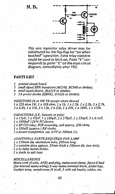
N. B.
This one transistor relay driver may be substituted for the flip-flop for "on when touched" operJtion. Extra relay cont.acts could be used to larch on. Point "X" car• responds to point "X" on the main circuit diagram, immediately after TRJ.
PARTS LIST
I printed circuit board. 5 small signal NPN transistors (BCI 08, BC548 or similar). 4 small signal diodes, (BA219 or similar). · . 5 IA power diodes (EM401, OA626 or similar).
RESISTORS(¼ or ½W 5% except where shown)
+
I x220ohmJW, I x330ohm, I xlk, I xl.5k, I x2.2k,2x2.7k, 2 x 6.8k, Ix !Ok, 2 x I 2k, 2 x 22k, Ix 33k; Ix 100k, Ix 150k.
CAPACITORS (LV, Ceramic or poly) . , Ix ]5pF, Ix 47pF, Ix J00pF, 2 x 270pF, Ix 330pF, 3 x 0.luF,
I x I 000uF 12 VW PC electro. Ix SP C/O relay, PCB mounting, coil approx. 250 ohms. Ix 330uH (approx.) RF choke. J-x power transformer, sec. 6-9Vat J00mA (+).
ADDITIONAL PARTS REQUIRED FOR LAMP Ix 100mm dia. aluminium tube, 200mm long. 2 x wooden discs, approx. 25mm thick x 100mm dia. (see text). I x be lamp batten holder. I x shade to suit base.
MISCELLANEOUS Mains cord (3-wire, ANEJ and plug, mains cord clamp, figure 8 lead (for internal mains wiring) 3-way mains terminal block, solder lugs, tinplate scrap, woodscrews (8 in all, 3 with csk heads), solder, etc.
62
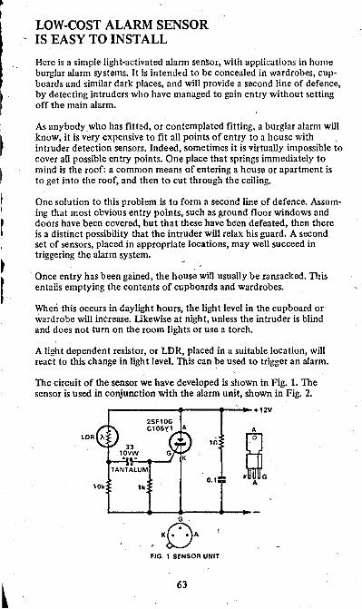
LOW-COST ALARM SENSOR IS EASY TO INST ALL
Here is a simple light-activated alarm sen~or, with applications in home burglar alarm systems. It is intended to be concealed in wardrobes, cupboards and similar dark places, and will provide a second line of defence, by detecting intruders who have managed to gain entry without setting off the main alarm.
As anybody_who has fitted, or contemplated fitting, a burglar alarm will know, it is very expensive to fit all points of entry to a house with intruder detection sensors. Indeed, sometimes it is virtually impossible to cover all possible entry points. One place that springs immediately to mind ls the roof: a common means of entering a house or apartment is to get into the roof, and then to cut through the ceiling.
One solution to this problem is to form a second line of defence. Assuming that most obvious entry points, such as ground floor windows and doors have been covered, but that these have be-en defeated, then there is a distinct possibility that the intruder will relax his guard. A second set of sensors, placed in appropriate locations, may well succeed in triggering the alarm system.
Once entry has been gained, the house will usually be ransacked. This entails emptying the contents of cupboards and wardrobes.
When this occurs in daylight hours, the light level in the cupboard or wardrobe will increase. Likewise at night, unless the intruder is blind and does not tum on the room lights or use a torch.
A light dependent resistor, or LDR, placed in a suitable location, will react to this change in light level. This can be used to trigger an alarm.
The circuit of the sensor we have developed is shown in Fig. I. The sensor is used in conjunction with the alarm unit, shown in Fig. 2.
,-------t---.... -- • 12V
••
2SF106 Cl06'!'.1 A
FIG. 1 SE"NSOR UNIT
63
.S. A
The LDR and the !Ok resistor form a voltage divider across the two wires supplying 12V DC to the sensor. The output from this divider is connected to the gate of a silicon controlled rectifier (SCR) by a 33uF tantalum capacitor. 111e lk resistor connected between the gate and the cathode of the SCR serves to stabilise its operation.
111e SCR is connected directly across the supply lines. The load for the anode circuit is pro_vided by a 12V relay, which is connected in series with the positive lead at the alarm unit.
Operation of the two units is as follows: when the LDR is in the dark, it has a high resistance, and the voltage on the positive end of the capacitor is low. The SCR is turned off. A sudden increase in' the light applied to the LDR generates a corresponding increase in the voltage applied to the capacitor. This increase is transmitted to the gate of the SCR, fuing it.
When the SCR fires, current is drawn through the relay, energising it, and setting off the alarm connected to the contacts. The SCR will remain triggered irrespective of tl1e light applied to the LDR. It can only be reset by momentarily interrupting the current through it, using the reset switch.
By using a capacitor in the gate circuit of the SCR, the sensor becomes insensitive to slow changes in light intensity. This will reduce the incidence of false triggering due to such things as changes in ambient light. If required, the capacitor can be deleted, and the LDR connected directly to the gate of the SCR.
'I'
i12Y ..... -~,--_ ___.J-
FIG. 2 ALA.RM UNIT
In the untriggered state, current consumption of the sensor unit is very small The leakage current of the SCR is of the order of 1 uA, while the current drawn by the LOR, which depends on the amount of light illuminating it, is normally about lOuA. This means that it is possible to use several sensor units in parallel with the one alarm unit. This can be triggered by any one sensor, the remaining sensors then being disabled.
Current consumption in the triggered state is principally determined by the relay, and any alarm bells used.
With some installations, where the distances between sensor units and the alarm unit are large, trouble may be experienced with false triggering due to transients induced onto the lines. The RC network connected across the SCR will eliminate almost all of this, as well as limiting the rate of rise of the anode/cathode voltage.
The components for the sensor units are conveniently mounted on small pieces of tagstrip or Vero board. Connect them to the alarm unit using either bell-wire or twin-lead. The leads should be colourcoded, and kept well away from any mains wiring.
Mount the sensor units in wardrobes and cupboards, concealing them as much as possible while still allowing light to reach the LOR when the doors are opened. Remember that the leads to the alarm unit must be concealed, or it will be possible to,defeat the sensor by cutting the leads.
The alarm unit can be mounted in any convenient place, and could form part of another alarm system. As the unit has very low current drain, it is possible to use dry batteries as the power source. Their life should equal the shelf-life,provided the alarm is not triggered too often.
65
AN ELECTRONIC ROULETTE WHEEL
Man has always been fascinated by games of chance, and one of the most popular forms of this mania is the wheel of fortune. Ranging from the simple chocolate wheel as used at fetes, to the complicated machines · employed by casinos, these devices always seem to attract large crowds of people willing to "have a go".
Much care is required in the construction of these machines, to ensure that the wheel runs true, so that the final result is completely random, and not biased in any way. Anyone who has seen a roulette wheel in a casino will appreciate the skill and workmanship required.
Our Electronic Roulette Wheel has no moving parts, arid thus does not require the same skills in construction. It is based upon an electronic number generator, which cannot be "fiddled" in any way. Admittedly, it does not have the same visual appeal as a large wheel which gradually slows down before stopping at the final number, but at the same time it is considerably less expensive, and does have a visual appeal of its own.
Our unit consists of a fairly large box, fitted with thirty-six small lights, arranged in a circle. The circle is divided into alternate black and white segments, with each segment being numbered at random from one to thirty-six. Only one of these lights is illuminated at any one time.
When the PLAY button is pressed, the lights appear to move rapidly round the circle. Once the button has been released, the lights start to slow down, just like a true roulette wheel, and eventually come to a stop at some randomly selected number.
••
1 OF 1BOECOOEA
PUY
4 CLOCK DIVIDE IY 111 COUNTEPI
A£SfT fLlPl'I..OP
FIG 1
66
·~·
I
I
Fig. 1 is a block diagram explaining the way in which we have impl<>mented the necessary functions. The clock generator is controlled by the PLAY switch. When the switch is depressed, the oscillator runs at a high speed, and feeds pulses to the divide-by-eighteen counter. After the switch is released, a time constant in the clock circuit makes the clock slow down to a stop in about 14 seconds.
The outputs from the counter are fed to a decoder, which has eighteen outputs. These are normally high, and each one goes low in turn as the counter cycles through its states. When the counter has reached eight· een, it is reset, and starts counting again.
This reset signal is also used to trigger a fliP"flop, which thus changes state every time the counter re-cycles. The complementary outputs from the fliP"flop are used to gate the outputs from the decoder, so that only one of the lamps connected to each decoder output is energised at a time. When the Q output of the flip-flop is high, lamps I to 18 are energised sequentially. The counter then resets, the flip-flop changes state, and lamps 19 to 36 are energised sequentially. The cycle then repeats for as long as clock pulses are supplied.
Physically, the lamps are arranged in a circle, so that each one is illuminated in turn. Visually, the energised light appears to be rotating in the same way as a normal roulette wheel does.
Initially, when the clock is running at a high speed, it is impossible to distinguish between individual lights, all one sees is a blur of light in a circle. However, as the clock slows down, one is able to see a rotating pattern, until eventually, the individual lights can be seen. Finally, only one light will remain illuminated,
This final light is randomly selected because it is impossible to ascertain exactly when the PLAY switch is released. This uncertainty is due to the high initial clock speed. Extensive (and time consuming!) tests with our prototype failed to show any bias whatsoever.
Since our design is only capable of providing an even number of digits we decided not to have any zeros on our wheel. Zeros are normally provided to give a bias in favour of the casino. Having no zeros ineans that our wheel will not favour the banker over any player .
. We decided to use TTL logic to implement our design, on the grounds that it is readily available, economical, and is capable of driving light emitting diodes (LEDs) directly. Although it has a high power consumption, we felt that for a mains powered device, this would not be too great a disadvantage.
The other main decision to make concerned the type of lights to be used. While incandescent lamps are quite cheap, they are not capable of inter· facing directly with TTL logic, due to their high current drain. In this
67
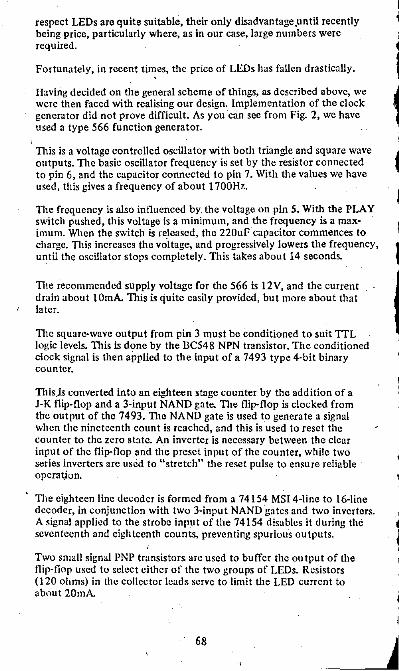
respect LEDs are quite suitable, their only disadvantage .until recently being price, particularly where, as in our case, large numbers were required.
Fortunately, in recent times, the price of LEDs has fallen drastically.
Having decided on the general scheme of things, as described above, we were then faced with realising our design. Implementation of the clock generator did not prove difficult. As you can see from Fig. 2, we have used a type 566 function generator.
This is a voltage controlled oscillator with both triangle and square wave outputs. The basic oscillator frequency is set by the resistor connected to pin 6, and the capacitor connected to pin 7. With the values we have used, this gives a frequency of about ! 700Hz.
The frequency is also influenced by. the voltage on pin 5. With the PLAY switch pushed, this voltage is a minimum, and _the frequency is a maximum. When the switch is released, the 220uF capacitor commences to charge. This increases the vOitage, and progressively lowers the frequency, until the oscillator stops completely. This takes about 14 seconds.
The recommended supply voltage for the 566 is 12V, and the current drain about !0mA. This is quite easily provided, but more about that later.
The square-wave output from pin 3 must be conditioned to suit TTL logic levels. This is done by the BC548 NPN transistor. The conditioned clock signal is then applied to the input of a 7493 type 4-bit binary counter.
This)s converted into an eighteen stage counter by the addition of a J-K flip-flop and a 3-input NANO gate. The flip-flop is clocked from the output of the 7493. The NANO gate is used to generate a signal when the nineteenth count is reached, and this is used to reset the counter to the zero state. An inverter is necessary between the clear input of the flip-flop and tlie preset input of the counter, while two series inverters are uscid to "stretch" the reset pulse to ensure reliable operation.
The eighteen line decoder is formed from a 74154 MS! 4-line to 16-line decoder, in conjunction with two 3-input NANO ·gates and two inverters. A signal applied to the strobe input of the 74154 disables it during the seventeenth and eighteenth counts, preventing spurious outputs.
Two small signal PNP transistors arc used to buffer the output of the flip-flop used to select either of the two groups of LEDs. Resistors (I 20 ohms) in the collector leads serve to limit the LED current to about 20mA.
68
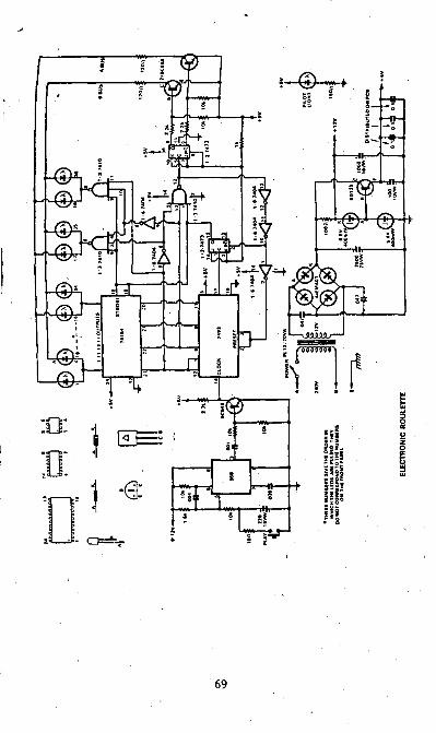
69

The configuration adopted is quite economical in terms of package utilization, only 6 !Cs are used, and all of these are used fully except for one inverter. Total current drain of the circuit is about 130mA, from a SV rail
We have used a LED as a pilot light, and placed it in the centre of the circle of LEDs. While this is not strictly necessary, as one of the other LEDs will always be illuminated, we felt that it improved the look of the circle, by providing a point of interest at the centre. If desired, it can be deleted.
We have used a fairly simple power supply. A full-wave bridge rectifier feeding into a 2500uF electrolytic capacitor supplies a nominal 20V from a 12V rms transformer. Two 400mW zen.er diodes in series provide nominal outputs of 5.6V and 12.4 V. The latter is used to power the 566 clock generator direct. Extra filtering for this is supplied by the lO00uF electrolytic capacitor.
The 5.6V zener drives a series pass transistor, giving a nominal output of SY. This is stabilised by the l00uF electrolytic capacitor at the output. We have used one of the plastic type transistors, as this is easily mounted on a suitable heatsink. The collector-emitter power dissipation is approximately 2 watts.
We mounted our prototype in a standard die-cast box, measuring 170 x 272 x 55mm. We mounted the LEDs on the bottom of the box, towards one end. We used two push switches, identical in appearance, for the POWER and PLAY functions.
We made a front panel for our device using aluminium.
Construction should be relatively simple, as all major parts are mounted on the printed circuit board. This measures }40 x 140mm. There are eight wire links on the board, which need not be insulated. The three electrolytic capacitors in the power supply must be pigtail types, rather than PCB types, as the headroom is limited.
The series pass transistor for the power supply mounts in one corner of the board. A small "L" shaped heat-sink must be fashioned from aluminium. The transistor is mounted on this with a mica washer and heat-sink compound. TI1e heat-sink is then screwed to the case, with a little heat-sink compound ensuring a reliable thermal bond.
All other components can be soldered directly on the board. We suggest that the !Cs are left until last, to minimise the risk of overheating. Remember to check the polarity of critical components, such as diodes and electrolytic capacitors .. Use circuit board pins for all external connections to the board. ·
70
1 '
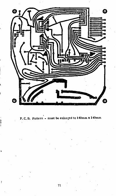
' P. C. B. Pattern - must be enl:1r1:Cd to 140mm x 140mm
71
t Of Components Layou
72
•
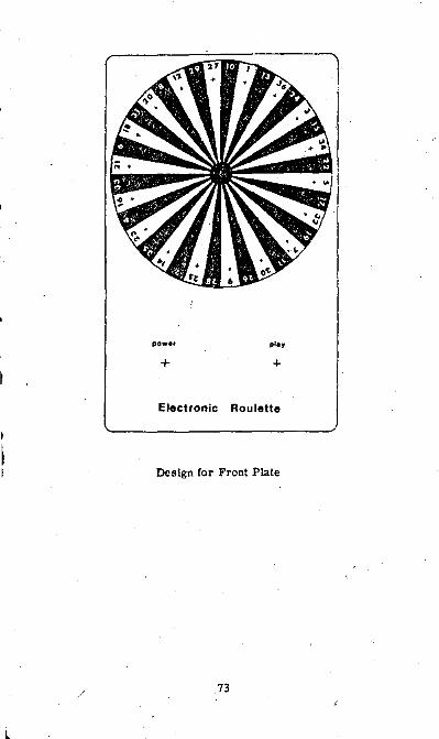
I
l
I
power play
+ +
Electronic Roulette
Design for Front Plate
73
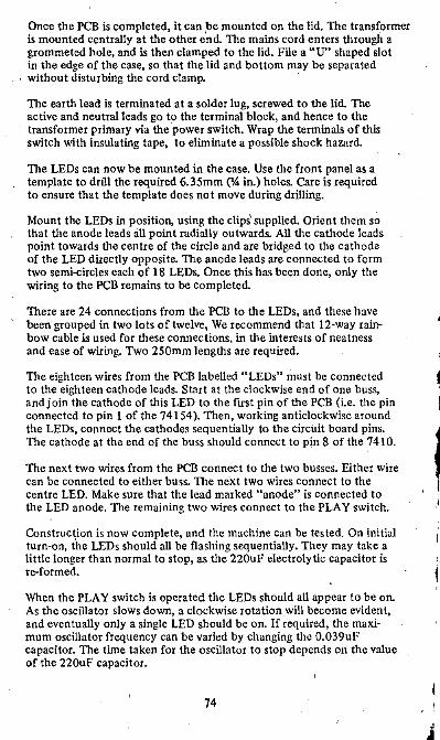
Once the PCB is completed, it can ,be mounted on the lid. The transformer is mounted centrally at the other end. The mains cord enters through a grommeted hole, and is then clamped to the lid. File a "U" shaped slot in the edge of the case, so that the lid and bottom may be separated
, without disturbing the cord clamp.
The earth lead is terminated at a solder lug, screwed to the lid. The active and neutral leads go to the terminal block, and hence to the transformer primary via the power switch. Wrap the terminals of this switch with insulating tape, to eliminate a possible shock hazard.
The LEDs can now be mounted in the case. Use the front panel as a template to drill the required 6.35mm (¼ in.) holes. Care is required to ensure that the template does not move during drilling.
Mount the LEDs in position, using the clips'supplied. Orient them so that the anode leads all point radially outwards. All the cathode leads point towards the centre of the circle and are bridged to the cathode of the LED directly opposite. The anode leads are connected to form two semi-circles each of 18 LEDs. Once this has been done, only the wiring to the PCB remains to be completed.
There are 24 connections from the PCB to the LEDs, and these have been grouped in two lots of twelve, We recommend that 12-way rain· bow cable is used for these connections, in the interests of neatness and ease of wiring. Two 250mm lengths are required.
The eighteen wires from the PCB labelled "LEDs" must be connected to the eighteen cathode leads. Start at the clockwise end of one buss, and join the cathode of this LED to the first pin of the PCB (i.e. the pin connected to pin 1 of the 74154). Then, working anticlockwise around the LEDs, connect the cathodes sequentially to the circuit board pins. The cathode at the end of the buss should connect to pin 8 of the 7410.
The next two wires from the PCB connect to the two busses. Either wire can be connected to either buss. The next two wires connect to the centre LED. Make sure that the lead marked "anode" is connected to the LED anode. The remaining two wires connect to the PLAY switch.
Construction is now complete, and the machine can be tcs ted. On initial turn-on, the LEDs should all be flashing sequentially. They may take a little longer than normal to stop, as the 220uF electrolytic capacitor is re-formed.
When the PLAY switch is operated the LEDs should all appear to be on. As the oscillator slows down, a clockwise rotation will become evident, and eventually only a single LED should be on. If required, the maximum oscillator frequency can be varied by changing the 0.039uF capacitor. The time taken for the oscillator to stop depends on the value of the 220uF capacitor.
74

You can now commence .to play roulette, using your unbiased wheel. For those readers who are unsure of the rules and manner of play, we have prepared a short article and a table layout.
PARTS LIST
SEMICONDUCTORS 1 74154 l•ofl6 decoder. 1 7493 4 bit binary counter. I 74 73 dual J-K flip-flop. 1 · 7410 triple three-input NAND gate. 1 7404 hex inverter. 1 566 function generator. 1 BD135 NPN power transistor, or equivalent. 1 BC548 NPN transistor, or equivalent. 2 BC558 PNP transistors, or equivalents. 4 EM401 silicon diodes, or equivalent. 37 LEDs, with mounting clips. See text. 1 5.6 V 400mW zenerdiode, BZX79C5V6 or equivalent. 1 6.8V 400mW zener diode, BZX79C6V8 or equivalent.
CAPACITORS 1 2500uF 25VW pigtail electrolytic. 1 lO0OuF 16VW pigtail electrolytic: 1 220uF 16 VW PCB electrolytic. 1 1OOuF10 VW pigtail electrolytic. 3 0. 1 uF plastic. 2 0. 04 7uF ceramic. 1 0. 039uF plastic. 2 0. 00JuF plastic.
RESISTORS(½ watt rating} 6 Wk, 1 2. 7k, 2 2.2k, 1 1.5k, 1 1 k, 1150 ohm, 2 120 ohm, 1100 ohm, 110 ohm.
MISCELLANEOUS 1 printed circuit board, coded 76rt3, 140 x 140mm. 1 transformer, 240V to 12V, Pll 2/20VA or equivalent. 1 diecast box, 170 x 2 72 x 55mm 1 front panel, see text. 1 240Vrated, push on-push off switch. 1 N/O momentary contact push switch to match. 1 mains plug, 3-core flex, grommet, cord clamp and 3-way terminal
block. 4 rubber feet. Scrap aluminium, machine screws, nuts, washers, solder, hookup wire, rainbow cable, mica washer, silicon grease, circuit board pins.
75
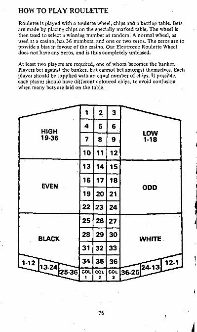
HOW TO PLAY ROULETTE
Roulette is played with a roulette wheel, chips and a betting table. Bets are made by placing chips on the specially marked table .. The wheel is then used to select a winning number at random; A normal wh·eel, as used at a casino, has 36 numbers, and one or two zeros. The zeros are to provide a bias in favour of the casino. Our Electronic Roulette Wheel does not have any zeros, and is thus completely unbiased.
At least two players are required, one of whom becomes the banker. Players bet against the banker, but cannot bet amongst themselves. Each player should be supplied with an equal number of chips. If possible, each player should have different coloured chips, to avoid confusion when many bets are laid on the table.
1
4 HIGH 19-36 7
10
' 13
16 EVEN
19
22
25
BLACK 28
31
34
COL ,
2
5
8
11
14
17
20
23
26
29
32
35 COL
2
76
3
6
9
12
15
18
21
24
27
30
33
36 COL
3
LOW 1-18
ODD
WHITE.
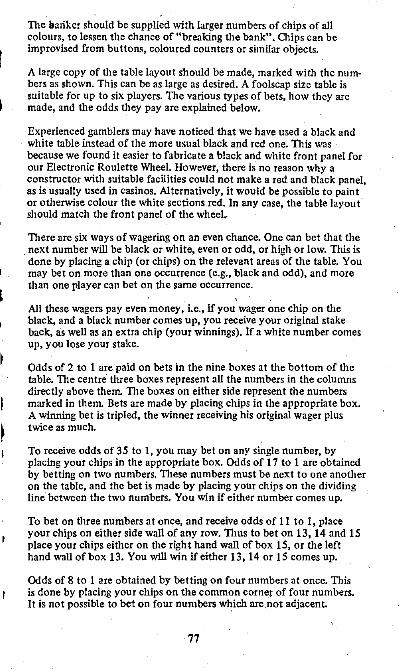
The l,arikcr should be supplied with larger numbers of chips of all colours, to lessen the chance of "breaking the bank". Chips can be improvised from buttons, coloured counters or similar objects.
A large copy of the table layout should be made, marked with the numbers as shown. This can be as large as desired. A foolscap size table is suitable for up to six players. The various types of bets, how they are made, and the odds they pay are explained below.
Experienced gamblers may have noticed that we have used a black and white table instead of the more usual black and red one. This was because we found it easier to fabricate a black and white front panel for our Electronic Roulette Wheel. However, there is no reason why a constructor with suitable facilities could not make a red and black panel, as is usually used in casinos. Alternatively, it would be possible to paint or otherwise colour the white sections red. In any case, the table layout should match the front panel of the wheel,
There are six ways of wagering on an even chance. One can bet that the next number will be black or white, even or odd, or high or low. This is done by placing a chip (or chips) on the relevant areas of the table. You may bet on more than one occurrence (e.g., black and odd), and more than one player can bet on the same occurrence.
All these wagers pay even money, i.e., if you wager one chip on the black, and a black number comes up, you receive your original stake back, as well as an extra chip (your winnings). If a white number comes up, you lose your stake.
Odds of 2 to 1 are paid on bets in the nine boxes at the bottom of the table. The centre three boxes represent all the numbers in the columns directly above them. The boxes on either side represent the numbers marked in them. Bets are made by placing chips in the appropriate box. A winning bet is tripled, the winner receiving his original wager plus twice as much.
To receive odds of 35 to 1, you may bet on any single number, by placing your chips in the appropriate box. Odds of 17 to 1 are obtained by betting on two numbers. These numbers must be next to one another on the table, and the bet is made by placing your chips on the dividing line between the two numbers. You win if either number comes up.
To bet on three numbers at once, and receive odds of 11 to 1, place your chips on either side wall of any row. Thus to bet on 13, 14 and 15 place your chips either on the right hand wall of box 15, or the left hand wall of box 13. You will win if either 13, 14 or 15 comes up,
Odds of 8 to 1 are obtained by betting on four numbers at once. This is done by placing your chips on the common corner of four numbers. It is not possible to bet on four numbers which are.not adjacent.
77

By placing your chips on the side walls so that they cover two rows, you receive odds of 5 to 1, and win if any of the numbers in either of the rows comes up.
These are the only bets which can be n\ade. A player may make as many bets at one time as he desires, and as many players as wish can bet on any one number or combination of numbers. When all bets have been laid, the banker calls "no more bets", and spins the wheel.
When the wheel stops spinning, the banker calls the winning number, e.g., "ten on the black", and then removes all losing wagers from the table. He then pays out all the winning bets to those fortunate few. No more bets should be laid on the table until all winning bets have been paid. This will avoid confusion, and prevent unscrupulous players from making bets after the result has been decided.
The game can then continue, until either all the players or the banker goes broke.
78
j

A SIMPLE ELECTRONIC MOSQUITO REPELLER
Summer is here, and as we make our escape into the great outdoors a small, but by no means insignificant, pest makes his presence felt. This year, however, we have a :new weapon ~th which to wage war on mosquitos. A clever amalgamation of sex and electronics has produced a mosquito repeller which is designed to create a ufree area" - indoors or out. ,
Years of university research has established that mosquitos can be repelled by sound. After mating, but before her eggs can incubate, a female mosquito needs blood. This is usually obtained from a convenient warm-blooded animal - you! During this time, the female will shun all male mosquito, (no doubt much to the chagrin of the males!). These desolate fellows, searching for conjugal bliss, emit a charcteristic sound.
Intensive study has determined that this sound has a frequency in the range 21 to 23 kilohertz. Our electronic device generates a similar sound and in fact simulates a large crowd of males. This of course will attract large numbers of mosquitos of both sexes.
In the interests of decency, we will not give details,of all that occurs when the sexes meet. Suffice it to say that pregnant mosquitos (female of course!), which are the only type that bite, are repelled by the large numbers of males, real and simulated, and search further afield for their source of blood.
This means that all the lucky people sufficiently close to the repeller are safe, and should not be bitten.
Turning now to the diagram, we can see how the required supersonic sound source has been realised. TRl, a unijunction transistor, functions as a relaxation oscillator. Operating frequency is determined by the R-C network connected to the emitter. The frequency stability with respect to voltage and temperature of this type of oscillator is more than adequate for the job in hand.
Initially, the capacitor is discharged, and no current flows in the emitter. As the capacitor charges through tl1e resistance, the emitter voltage rises. When this reaches the peak point voltage, TRl fires; and discharges the capacitor through the circuit connected to Bl.
As the capacitor is discharged, theinitially high emitter current falls. When this current drops below the valley-point current, TRl turns off, and the cycle starts again. The output voltage, obtained at Bl, is a series of short pulses.
79
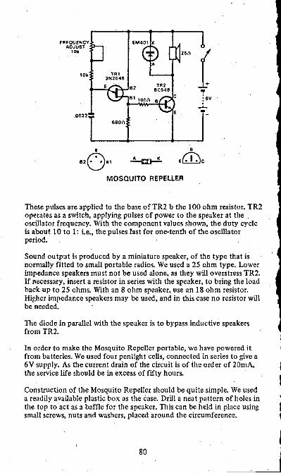
FREOUE"ICY ADJUST
10k
10k
.0022 680(\
• a2Qa1 MOSQUITO REPELLER
These pulses are applied to the base ofTR2 b the 100 ohm resistor. TR2 operates as a switch, applying pulses of power to the speaker at the oscillator frequency. With the component values shown, the duty cycle is about 10 to 1: i.e., the pulses last for one-tenth of the oscillator period.
Sound output is produced by a miniature speaker, of the type that is normally fitted to small portable radios. We used a 25 ohm type. Lower impedance speakers must not be used alone, as they will overstress TR2. If necessary, insert a resistor in series with the speaker, to bring the load back up to 25 ohms. With an 8 ohm speaker, use an 18 ohm resistor. Higher impedance speakers may be used, and in this case no resistor will be needed.
The diode in parallel with the speaker is to bypass inductive speakers from TR2.
In order to make the Mosquito Repellcr portable, we have powered it from batteries. We used four penlight cells, connected in series to give a 6V supply. As the current drain of the circuit is of the order of 20mA, the service life should be in excess of fifty hours.
Construction of the Mosquito Repellcr should be quite simple. We used a readily available plastic box as the case. Drill a neat pattern of holes in the top to act as a baffle for the speaker. This can be held in place using small screws, nuts and washers, placed around the circumference.
•
1
80 _J
I I
'
We assembled the electronics on a small piece of Vero board. As the circuit is very simple, we have not provided any details of the actual placing of the components.. Connections to the various elements not on the Veroboard can be made using hookup wire.
The Veroboard is supported on a spacer fitted to one of the speaker mounting screws.. Mount the board upside down, and orient it so that access to the trimpot can be gained through a small hole in the case. This will facilitate adjustments to the operating frequency.
The mounting screw for the Veroboard can also serve to hold the back panel on. The on-off switch can be held in place using self-tapping screws.
Suitable labels can be applied to the front of the case, using stick-on lettering. When finished, this can be protected by spraying with clear lacquer. This completes construction, and the device is now ready for testing.
As the sound produced by the Mosquito Repeller is higher pitched than most people can hear, there will be no immediate indication that it is operating correctly. If desired, the timing capacitor may be temporarily increased in value to 0,0luF. This will lower the operating frequency into the audible range, and enable you to hear the device operating.
Once satisfied that all is working correctly, replace the 0.0022uF capacitor, and adjust the !Ok trimpot so that the frequency is about 22kHz. If you do not have access to any frequency measuring equipment, set the pot to the middle of its range. If necessary further adjustments can be made under field conditions, in the presence of mosquitos!
PARTS LIST
1 unijunction transistor, 2N2646, DS2646 or equivalent. I NPN transistor, BC548 or equivalent. I silicon diode, EM401 or equivalent. I JOO ohm, 1680ohm, J0k resistor. I I Ok trimpot. 1 0. 0022uF plastic capacitor. I miniature speaker, (see text). 1 case. 4 penlight cells, holder and connection clip., I piece Veroboard. 1 switch, single pole single throw.
MISCEUANEOUS Hookup wire. solder, machine screws, nuts, w~shers, threaded spacers, foam rubber.
81
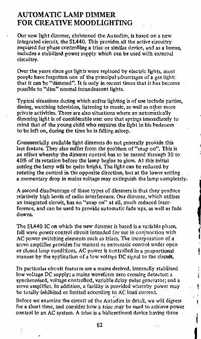
AUTOMATIC LAMP DIMMER FOR CREATIVE MOODLIGHTING
Our new light dimmer, christened the Autodim, is based on a new integrated circuit, the SIA40. This provides all the active circuitry required for phase controlling a triac or similar device, and as a bonus, includes a stabilised power supply which can be used with external circuitry.
Over the years since gas lights were replaced by electric lights, most people have forgotten one of the principal advantages of a gas light: that it can be "dimmed". It is only in recent times that it has become possible to "dim" normal incandescent lights.
Typical situations during which softer lighting is of use include parties, dining, watching television. listening to music, as well as other more private activities. There are also situations where an autom3.tically dimming light is of considerable use: one that springs immediately to mind that of the young child who requires the light in his bedroom to be left on, during the time he is falling asleep.
Commercially available light dimmers do not generally provide this last feature. They also suffer from the problem of "snap on". This is an effect whereby the dimmer control has to be turned through 30 to 40% of its rotation before the lamp begins to glow. At this initial setting the lamp will be quite bright The light can be reduced by rotating the control in the opposite direction, but at the lower setting a momentary drop in mains voltage may extinguish the lamp completely.
A second disadvantage of these types of dimmers is that they produce relatively high levels of radio interference. Our dimmer, which u.tilises an integrated circuit, has no "snap onu at all, much reduced interference, and can be used to provide automatic fade ups, as well as fade downs.
The SIA40 IC on which the new dimmer is based is a variable phase, full wave power control circuit intended for use in conjunction with AC power switching elements such as triacs. The incorporation of a -servo amplifier provides for manual or automatic control under open or closed loop conditions. AC power is controlled in a proportional manner by the application of a low voltage DC signal to the circuit.
Its particular circuit rCatures are a mains derived, internally stabilised low voltage DC supply; a mains waveform zero crossing detector; a synchronised, voltage controlled, variable delay pulse generator; and a servo amplifier. In addition, a facility is provided whereby power may be totally inl1ibited or limited according'.?· AC load current,
Before we examine the circuit of the Autodim in detail, we will digress for a short time, and consider how a triac may be used to achieve power control in an AC system. A triac is a bidirectional device having three
82 I I
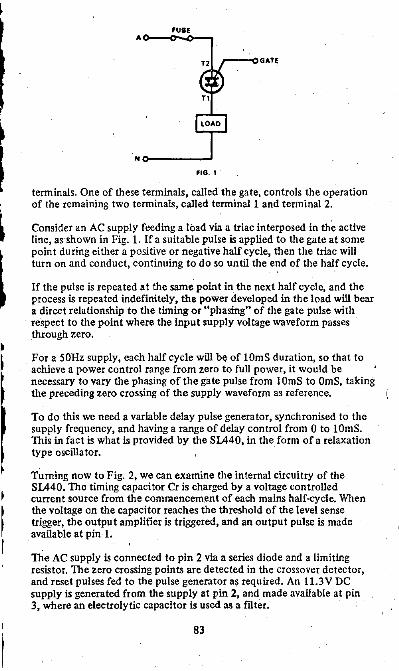
GATE
FIG. 1
terminals. One of these terminals, called the gate, controls the operation of the remaining two terminals, called terminal l and terminal 2.
Consider an AC supply feeding a load via a triac interposed in the active line, as shown in Fig. 1. If a suitable pulse is applied to the gate at some point during either a positive or negative half cycle, then the triac will turn on and conduct, continuing to do so until the end of the half cycle.
If the pulse is repeated at the same point in. the next half cycle, and the process is repeated indefinitely, the power developed in the load will bear a direct relationship to the timing or "phasing" of the gate pulse with respect to the point where the input supply voltage waveform passes through zero.
For a 50Hz supply, each half cycle will be of IOmS duration, so that to achieve a power control range from zero to full power, it would be necessary to vary the phasing of the gate pulse from l OmS to Oms, taking the preceding zero crossing of the supply waveform as reference.
To do this we need a variable delay pulse generator, synchronised to the supply frequency, and having a range of delay control from O to l Oms. This in fact is what is provided by the SL440, in the form of a relaxation type oscillator.
Turning now to Fig. 2, we can examine the internal circuitry of the SL440. The timing capacitor Cr is charged by a voltage controlled current source from the commencement of each mains half-cycle. When the voltage on the capacitor reaches the threshold of the level sense trigger, the output amplifier is triggered, and an output pulse is made available at pin 1.
The AC supply is connected to pin 2 via a series diode and a limiting resistor. The zero crossing points are detected in the crossover detector, and reset pulses fed to the pulse generator as required. An 11.3V DC supply is generated from the supply at pin 2, and made available at pin 3, where an electrolytic capacitor is used as a filter.
83
LOAD CUR"ENT
12 SERVO
~:~~ I IIM'ERTINGJ I SERVO
Fig. 2:
I AMPllFIER
I I
I L __ _ 13
SE"VO ERROR OUTPUT
AC r-----C::J--kr--o. SUPPlY
l -----------,
+ll·JV
SUPPLY TO CIRCUITS
I I
I
TRIGGER PULSE OU1PU1
AMPUFIER 1
CONTffOI. : ELEMENT
VARIABLE OElAY PULSE
GENERATOR
I
fl I _ _______ J
14
TIMING I CAPACl~M Cy
Pin 12 is the inverted input to the servo amplifier. The output of this amplifier is available at pin 13, which is internally connected to the control input of the variable delay pulse generator. Also connected to this point is the output from the current limit detector and buffer.
Fig. 3 gives the complete circuit of the Autodim. Overload protection is supplied by the 2A fuse connected in series with the active line. The 6.8k SW resistor used to limit the supply current is composed of 5 x 33k 1 W resistors connected in parallel. This is. cheaper and gives better heat dissipation than the equivalent SW resistor.
The 11.3V DC supply from pin 3 is ftltered by the 4 70uF electrolytic capacitor. The diode, resistor and capacitor network we have shown connected to pin 4 provides a soft start facility on initial turn on. If this is not required, these components can be deleted, and pin 4 connected directly to pin 3.
Sl is a three pole three position switch, used to select the mode of operation of the dimmer. In the "manual" position, the servo amplifier is disabled by connecting its input to the neutral line, and the lamp brilliance is controlled directly by the potentiometer. One end of this pot. is connected to the 11.3V rail by an 18k limiting resistor, while the other end is connected to the active line via two silicon diodes and an
84 I
r 85
·o· :: . -
. •
:; 0 0 ... :, <
internal diode connected to pin 10. This ensures that maximum power always occurs at the end of the pot. travel, and also provides some thermal compensation.
In the "increase" position, the servo amplifier is conitected as a Miller integrator. This means that the output of the servo amplifier, and hence
_ the input to the pulse generator, changes linearly with time, so that the lamp brightness increases progressively from zero to maximum. The time that this takes to occur is determined by Rae, and for the values we have used, it takes about 13 seconds.
In the "decrease" position, the time taken for the lamp brightness to fall from maximum to minimum is given by 20RaC, and for the values we have used, this takes about 45 minutes. The maximum achievable fade rate is limited by the input in1pedance of the SlA40, and by the leakage resistance of the capacitor.
The 1.8k limiting resistor shown in series with the control pot. is required to prevent damage to the internal diode connected to pin 10 of the SlA40. Damage can occur when the pot. is set to maximum intensity, and switch Sl is operated. This is because the readily available rotary switches are shorting types, with contacts that "make before break". If a "break before make" type switch is available, this resistor is not necessary.
The output buffer amplifier connected to pirt 1 is composed of a single transistor with an uncommitted collector. The 4. 7k resistor connected to the 11.3V rail forms the load for this stage. When an output pulse is generated, the transistor shorts pin 1 to pin 3. The resulting pulse genera· ted at the negative end of the l0uF electrolytic capacitor is transmitted to the gate of the triac via the 4 7 ohm resistor. The 150 ohm resistor ties the gate to Tl, and ensures reliable triggering.
i Interference suppression is provided by the inductor in series with the active lead. The RC network connected across the triac is a snubbing net· work. This will eliminate the possibility that the dv/dt rating of the triac is exceeded.
The SlA40 is manufactured by Plessey.
The triacs we have specified in the parts list are plastic pack types, and have the advantage that they can be used without any form of heatsink for resistive or incandescent loads up to 300W. Higher loads, up to 1000W, may be used, provided the triac is mounted on an adequate (and well insulated) heatsink.
Construction of the Autodim sh~uld not present any difficulties. All major components are mounted on a small printed circuit board, 121 x 64mm.
86
-. I
. ; P. C. B. Pattern .
' 87
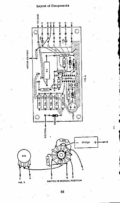
E
FIG. 5
A
Layout of Components
- 2500µF + G
B D
SWITCH IN MANUAL POSITION
88
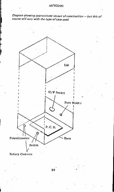
AUTOD!l\l
Diagram showing approximate layout of construction - but this of course will vary with the type of case used.
1 0/P Socket
Potentiometer
~ Switch
Rotary Controls
89

We used a case measuring 105 x 137 x 60mm, and consisting of a crackle-lacquer finished steel lower section with a brushed aluminium top section.
The PCB is mounted on the base of the case, with the mains input cable, clamp, terminal block and fuse assembly mounted on the rear section. The PCB must be positioned sufficiently far forward to clear the mains output socket, which is also mounted on the rear panel. The t\vo rq,tary controls are mounted towards the top of the front panel, to allow clearance for the PCB underneath.
Construction is best started by fitting all the hardware to the case. The !'CB is spaced off the bottom of the case using nuts as spacers. At least 5mm clearance is required, to ensure adequate insulation to the case.
The mains cord !nters through a grommetted hole in the rear left hand corner, and must be securely clamped. The earth lead is terminated in a solder lug, which is clamped to the case at the cord clamp. The active and neutral leads are routed direct to the terminal block, which must have three connections.
The chassis mounted fuse is connected between the active terminal connection and the remaining spare terminal. The earth lead from the output socket is terminated with a solder lug, and clamped to the case with the input earth. The neutral lead from the output socket is connected to the neutral connection of.the terminal block.
Toe remaining connections from the terminal block and the output socket can be left unconnected, till the PCB is installed.
Ll, the interference suppression inductance, is not available commercially but is quite easily made. A 50mm length of 10mm dia. ferrite rod is required. If a longer length has been obtained, it can be cut by filing a groove around the circumference, and then snapping it as if it were glass'.
Wind a layer or two of plastic insulation tape around the rod. Then close wind a layer of 2 S.W.G. enamelled copper wire over the insulation tape. The actual number of turns is not critical; use as many as will fit comfortably.
Now wind another two layers of insulation tape over the copper wire, making sure that the tape is wound very firmly. If this is not done, the inductor will emit a buzzing sound due to the currents being switched by the triac.
The last step is to clean the leads to remove the enamel, and then to tin them with solder. An easy way to remove enamel is to scrape the wire with a sharp instrument, such as a razor blade (be careful, and use a single sided safety blade if possible).
90
I
I
'
'
We can now turn our attention to the PCB, and commence to fit components. The five I W resistors should be mounted a little proud of the board, to allow for air circulation. There should be no difficulties with the remaining components. The only point to watch is that polarity
/ conscious components are inserted correctly.
The triac can be soldered directly to the board, as can the SL440. If you have followed the dimensions given for the interference suppression inductance, you will find that it is a neat fit on the board. We recom· mend the use of printed board stakes for all external connections to the board, as these give a neat appearance, and make for easy assembly.
At this point a few words are in order concerning'the arrangement of the external connections at the left hand end of the board. The arrangement used was chosen to provide flexibility in the wiring to the servo
' amplifier inputs and outputs, to allow the PCB to be used in a number of different ways. This has meant that a small number of links are required, as shown in the PCB overlay:
Using the accompanying diagram, the two rotary controls can now be wired up. Leave the leads to the PCB long enough to allow later servicing, if required. The 2500uF electrolytic capacitor is wired directly between the switch contacts and the PCB. The leads must be insulated with spaghetti tubing.
The remaining wiring to be completed is to the mains output socket and to the terminal block. Ensure that the active and neutral wires are not transposed. When all construction is finished, carry out a careful check for mistakes, and then fit the cover.
We made a front panel for the Autodim using a small panel from scrap aluminium, and apply the stick-on lettering direct. This will give a quite acceptable alternative.
Plug a small incandescent light into the output socket, set the level pot. to maximum and the mode switch to "manual", and then apply power. After a short delay, the lamp should come on. Astute readers may notice the soft turn on which will occur. Next, check that the level pot. does indeed control the light output, and that maximum and minimum levels occur at or near the end positions.
Now set the 1evel control to minimum, and switch to uincrease". After about 13 seconds, the lamp should have reached full brilliance. Once satisfied that full brilliance has been reached, switch to "decrease". The lamp should now fade at an imperceptible rate, finally going out after about 45 minutes.
91
A few words are now in order concerning troubleshooting and servicing of the Autodim. As there is no isolation transformer, and because the circuit operates directly from the mains, most of the circuitry will be at active potential. This means that servicing "'.ill be quite hazardous, and should be avoided if possible. Provided all components are fitted correctly, and all solder joints are good, there should be little to go wrong, as all the active circuitry is contained in the IC. '
If you do need to service the unit, we suggest you use an isolating trans• former to avoid the risk of a fatal shock.
LIST OF COMPONENTS
1 SL440 IC. (Plessey) J plastic pack triac, SCJ4JD, 40669 or similar. 1 silicon diode, EM404 or similar. 3 silicon diodes, EM401 or similar. I 0. 022uF polyester capacitor. 1 0. 1 uF 630 VW plastic capacitor. I 2500uF 16 VW electrolytic capacitor. I 470uF 16VWelectrolytic capacitor. 2 1 0uF J 6VW electrolytic capacitors. I 47 ohm ¼W resistor. 1 I 00 ohm ¼W resistor. 1 150 ohm ¼W resistor. 1 I.Bk ¼W resistor. 2 4. 7k ¼W resistors. 1 18k ¼W resistor. 1 22k ¼W resistor. 5 33k 1 W resistors. 1 68k ¼ W resistor. I 1 00k ¼W resistor. J 4 7k linear potentiometer. J 3-pole 3-position rotary switch. 2 knobs. 1 case (see text). 1 chassis mounting 240 V 3 pin socket. 1 fuse holder, chassis mounting, with 2A fuse. J mains plug, cord, grommett, clamp and terminal block. 1 printed circuit board, 121 x 64mm.
MISCELLANEOUS Machine screws, nuts, washers, solder lugs, hook_-up wire, insultation tape, spaghetti sleeving, 2 S. W. G. enamelled copper wire, ferrite rod, solder, circuit board pins.
NOTE: resistor wattage ratings and capacitor voltage ratings are those used in our prototype. Components with higher ratings may generally be used provided they are physically compatible. Components with lower ratings may also be used' in some cases, providing ratings are not exceeded.
92

r ,
Notes

Notes

Notes

Notes
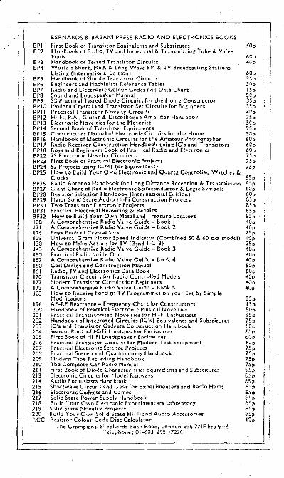
BPI BP2
BP) BP4
BPS BP6 BP7 BP8 BP9 BPIO BPI I BP l2 BPl3 BPl4 BPJ 5 BPl6 BPl7 BP!B BP22 BP23 eP24 BP25
BP26 BP27 BP23 BP29 BP30 BP31 BP32 100 121 126 129 139 143 ISO 157 160 161 170 177 179 183
196 200 201 202 203 204 205 206 207 203 209 210 211 213 21. 215 216 217 218 219 220 F.::c
e.ERNARDS & BABANI PRESS RADIO AND ELECTRON:cs eoo~
First 8ook of Transistor Equivalents and Substitutes ___ - 4,Cp I Handbook cf Radio, TV and lnduHrial & Tra'1smitting Tube & Valve 1
Equiv. lOp I Handbook of Tested Tramistor Circuits 40p I World's Short, Med. & Long Wave FM & TV Broadcasting Station, Listing (International Edition) (.Op Handbook of Simple Transistor Circuits 35p ' Engineers and Machinists Reference Tables 30p Radio and Electronic Colour Codes and Data Chart I So Sound and Loud~peaker Manual 50p 33 Practical Tested Diode Circuits for the Home Constructor 35p Modern Cryscal and Transistor Set Circuits for Beginners 35p Practical Transistor Novelty Circuits 4C-o Hi-Fi, P.A., Guitar & Discotheque Amplif;er Hand!:look 750 Electronic Novelties for the Motorist SCo Second Book of Transistor Equivalents 9Sp Constructors Manual of Electronic Circuits for the Home 52p Handbook of Electronic Circuits for the Amateur Photographer 6Cp Radio Receiver Construction Handbook using !C's and Transistors !Op Boys and Eeginners Book of Practical Radio and Electronics t:,Op 79 Electronic Novelty Circuiu 75p First Book of Practical Electronic Projects 750 52 Projects using lC741 (or Equivalents) 75p How to euild Your Own Electronic and Qu.arti Cc-ntro!led Watches & Clocks 8Sp Radio Antenna Handbook for Long Dis~ance Reception & Transmissioo 85p Giant Chart of Radio Electronic Semiconductor & Logic Symbols 60p ResiHor Selection Handbook (lnternational Edition) 60p Mator Solid St:ate Audio Hi-Fi Construction Projects S5p Two Transistor Electronic Projects E5p Practical Electrical Re-wiring & Repairs E.Sp How to Euild Your Own Metal and Tn•:uure locator1 bSp A Comprehensive Radio Valve Guidi! - Book I •Op A Compreh.ensive Radio Valve Guide - Bock 2 -40p Boys Boo~ of Crystal Sets 25p Universal Gram-Motor Speed Indicator {Combined 50 & 60 C? m00€1) I Op How to M:.ke Aeriafs for TV (3-md 1-2-3) 250 A Comprehensive Radio Valve Guide - Bock 3 40p Practical Radio Inside Out 400 A Ccrnpre!lensive Radio Valve Guide - Boe!( • 4Cp Coil Oesig, and ConHruction Manual SOp Radio, lV and Electronics Data Book f.(lp Transistor Circuits for Radio Controlled Models ~Op Modern Transistor Circuits fer Beginners '¼)p
A Comprehensive Radio Valve Guide - Book 5 ~Op How to Receive Foreign TV Programmes on your Set by Sim~le Modifications AF-RF Reacunce - Frequency Chart for Constructors Hand!:>oc-k of Practical Electronic Musical Novelties Practical Transistorised Novelties for Hi-Fi Enthusiasts Ha.nd~ock of Integrated Circuiu (IC's) Equivalents and SubstitutE>.:l !C's and Transistor Gadgets Construction Handbook Second Boc-k of Hl-fi Loudspeaker Enclosures first B;>ol< of Hi-Fi Loudspeaker Enclosures Practical Transistor Circuits for Modern Test Equipment Practical Electronic Science Prc,jects Practical Stereo and Quadrophony Handbo-o~ Modern Tape Recording Handbook The Complete Car Radio Manual First e:ook of Diode Characteristics Equivalents and Su~sticutes Electronic Circuits for Model Railways Audio Enthusiasts HJndbook Shortwave Circuits and Gearfor Experimenters a~d Radio Hams Electronic Gadgets and Garnes Solid State Power Supply HJndbook Build Your Own Electronic Experimenters lai:>o(a:cry Solid State Novelty Projects Build Your Own Solid State Hi-Fi and Aud:o Accessories Resistor Colour Coc'e D;sc U.lculator
The Grampians, S'1epherds £:mh Road, Lo,don Y\'6 7!\!F fr.gf;:nd T("iephone: 0!-iCJ 2:F.l,'TI?6

![Union Calendar No. TH D CONGRESS SESSION H. R. ll...Union Calendar No. ll 116TH CONGRESS 2D SESSION H. R. ll [Report No. 116–ll] Making appropriations for the Department of the Interior,](https://img.pdfslide.net/doc/110x75/5ff966d501553e0e807c5400/union-calendar-no-th-d-congress-session-h-r-ll-union-calendar-no-ll-116th.jpg)


![- r --]pkits r ,:.t, tr%s s.icc% · _-.,Xiqllj _al._j)ll _z..,1;,_l_llj_ljfiqll_ afi_)ll .!_l._.lIj 2j 'L_I Sl,._._! .:. %.9 ._,:11cT._l j'_l](https://img.pdfslide.net/doc/110x75/5f38394a5e257d13cb4b2383/r-pkits-r-t-trs-sicc-xiqllj-aljll-z1llljljfiqll-afill.jpg)


![Ll :[i][r]0Ll00l](https://img.pdfslide.net/doc/110x75/587f32341a28abc8108b6511/ll-ir0ll00l.jpg)