Embed Size (px)
Citation preview

Radiation Damage and Ion Behaviour in Ion Implanted Vanadiumand Nickel Single Crystals;Ion Implantation in Superconducting Thin Films
Oktober 1973
Institut für Angewandte Kernphysik
M. Gettings, I<.G. Langguth, G. LinkerO. Meyer, H. Mann, E. Phrilingos
KFK 2109

Als Manuskript ~ervielfältigt
Für diesen Bericht behalten wir uns alle Rechte IJ
GESELLSCHAFT FÜR KERNFORSCHUNG M
KARLSRUHE
Reprinted fram: APPLICATIONS OF ION BEAMS Ta METALSEdited by S. T. Picraux, E. P. EerNisse and F. L. Vaak
Book available from: Plenum Publishing Corporation227 West 17th Street, New York, New York 10011
RADIATION DAMAGE AND ION BEHAVIOUR IN ION IMPLANTED VANADIUM AND
NICKEL SINGLE CRYSTALS
M. Gettings, K.G. Langguth and G. Linker
Institut für Angewandte Kernphysik
Kernforschungszentrum Karlsruhe
ABSTRACT
Distributions and annealing behaviour of heavy ion inducedradiation damage in single crystal nickel and vanadium are compared.Sharp annealing stag~s are reported for Ni while for V the production of a pOlycrystalline layer, ascribed to the action of precipitates, prevented the annealing of damage after high dose implantations. The use of 4He+ ion channelling revealed disorder atdepths much greater than the ions projected range, an observationthat was supported by electron microscopy measurements. Implantedion diffusion in vanadium was found to be dependent on the ionspecies used and the annealing behaviour of precipitates. Preliminary quantitative measurements indicate that diffusion coefficientsare low.
INTRODUCTION
The investigation of radiation damage in transition metalsby heavy ion bombardment is rapidly becoming a useful means ofsimulating long term damage in reactor environments. Further,there appears to be a growing interest in alloying and isotope enrichment using high dose implantation. In this present study, radiation damage and ion diffusion have been studied in the reactorbase metals nickel and vanadium.
For fcc structured nickel, a number of electron microscopyinvestigations(1-3) dealing with radiation damage have been reported. At low ion doses in this metal, only vacancy clusters havebeen detected while for higher doses interstitial clusters are
241

242 M. GETTINGS, K. G. LANGGUTH, AND G. LINKER
dominant. In general, the majority of damage has been detectedwithin the ion projected range, although in other fee metals someinterstitial clusters at depth greater than the ion ranges, havebeen observed and explained by focussed collision sequences(4).
For bcc vanadium, however, only few results are presentlyavailable(5). In previous publications(6,7) dealing with singlecrystal vanadium, we have reported enhanced damage depths withincreasing ion energy and dose, a small dependence of the magnitude of damage on these parameters, the generation of a polycrystalline layer in the ion range for high dose implants and valuesof substitutional components dependent on the implanted ions ionicradii.
Results reported in this present work have been obtained usingthe backscattering technique from single crystal nickel implantedwith bismuth, and single crystal vanadium implanted with gallium,bismuth and selenium. Some preliminary electron microscopy measurements have been taken for gallium ion induced damage in vanadium. The backscattering technique has also been employed to monitor the distribution of the implanted ions and its subsequentvariations during heat treatment.
EXPERIMENTAL
Our backscattering system and the surface preparation of vana?ium single crystals have been described in detail elsewhere(7 . Like vanadium, nickel single crystals produced by electron
beam zone refining have been purchased from Metals Research Corporation. Nickel samples were cut perpendicular to the <110> direction with a continuous wire saw and subsequently lapped with15 ~ , 7 ~ , 1 ~ and 0.25 ~ diamond pastes. Samples were thenetched for 5 second periods in a solution consisting of 30 ce HN03,10 ce H2S04, 10 ce H3P03 and 50 ce glacial CH3COOH held between85 - 950C. Vanadium samples for our electron microscopy studieswere prepared by mechanically thinning from the not implantedside to 0.1 mm by careful polishing on SiC paper followed by avibratory polish with y-A1203 of 0.05 ~ diameter. Final thinningwas done electrolytically with a mixture of 80 % acetic acid and20 % perchloric acid. With this technique depth determination wasestimated to be about ±200 ~.
Implantations were performed at room temperature with ascanned ion beam from a heavy ion accelerator. Metal samples werebombarded over an energy range from 20 - 360 keV and a dose rangeof 1015 - 10 17 ions/cm2
• Irradiated specimens were annealed in astainless steel tube under a vacuum of ~ 6 x 10- 7 torr, isochronally, to temperatures of 10000C and isothermally for timeslasting to 18.5 hours.

RADIATION DAMAGE AND ION BEHAVIOR 243
6000(al 2 MeV'He
Bi
Bi
5.3 ·1016
Bi'lc",z in Ni360 KeV
200 250 300CHANNEL NUMBER
--- 4.0'1016Bi'tcm~300KeVin V-------- 2.0·1015Bi'lcrrf 300K Vin V
ALiGNED<110>
1502 MeV'He'
100
ALIGNED<100>
UNIMPLANTED ~0[==~50C==~~==;:=====L~:::::::~_-JL __
2000
3000
1000
4000
3000
5000
2000...JWZZ
~ 1000u....Vl.....z:::>815 5000 (b)wlD~:::>z
4000
250 300CHANNEL NUMBER
20015010050O+---.--------r--~--~==~=-===-----~-~o
Fig. 1 Backscattering spectra from aligned and randomly orientedsamples showing the damage produced in nickel and vanadium singlecrystals by bismuth ion bombardment.

244 M. GETTINGS, K. G. LANGGUTH, AND G. LINKER
RESULTS
The results reported in this paper will be presented in twodistinct sections:-
a) A comparison of damage and annealing innickel and vanadium
b) Diffusion of implanted components in vanadium
a): In an attempt to compare radiation damage producedduring ion implantation in vanadium and nickel, single crystalswere bombarded with similar doses of Bi ions having the same energy. Typical aligned and random backscattering spectra from bothnickel and vanadium are presented in figure 1 to show differencesin the generated damage distributions. In nickel close to the surface, in a depth region between 350 and 450 ~ for nonchannelled implants, a surface peak is found for all doses and energies underconsideration. The area of this peak increases with ion dose anddecreases with energy. In the case of channelled implantations onlythe deep damage has been observed. Near surface disorder in vanadium however, was found to be strongly dependent on ion dose. Fordoses lower than 1016 ions/cm2 , a narrow surface peak «200 ~)was detected, whereas for higher doses a polycrystalline layer wasformed over the range of the implanted ions. These surface peaksin both vanadium and nickel are thought to be disordered layersrather than oxides, as no enhanced oxrgen peaks were found usingthe helium-oxygen resonance at 3.06 MeV He+ ion energy.
The layer produced by high dose implantations in vanadium hasbeen investigated by X-ray diffraction and was found to be of apolycrystalline nature having the vanadium bcc structure. Weascribe this layer formation to the generation of precipitatesproduced when the solubility limit of Bi in vanadium is exceeded.Such precipitates are expected to partially destroy the hostlattice in the region of the implanted ions. These precipitatesand lattice distortions cause a backscattering rate equal to thatof a randomly oriented sample. As the dechannelling from these polycrystalline layers was found to be lower than that from evaporated vanadium layers of similar thicknesses, it is concluded thatthe single crystal has not been completely disrupted and coherentprecipitations of the implanted ions may occur.
For nickel, the absence of a polycrystalline layer is attributed to the lower concentration of bismuth ions in this material,as compared with vanadium for similar total doses. These lowerconcentrations and ion distribution broadening can in turn be explained by the high sputtering yields of Bi ions in nickel compared to Bi in vanadium(8). Besides the near surface damage,damage at depths considerably greater than the ion projected rangewas observed in both nickel and vanadium. Differences in the struc-

RADIATION DAMAGE AND ION BEHAVIOR 245
GooA
CHANNEL NO.
Vedge
/~OA
Vanadium implanted with1·101
? Ga 300keV
o+------------------'==------'-,--UNIMPLANTED
1000
2000
3000
::r:S:2~z:::>8
4000
Fig. 2 Electron microscopy photographs from unimplanted and implanted (10 17 Ga/ern 2, 300 keV) vanadium samples together with abackscattering spectrum indicating the depths at which photographswere taken.
ture of this deep damage, as revealed in the backscattering spectra,were observed for the two metals investigated. For vanadium, inthe absence of a polycrystalline layer, a relatively damage-freeregion was observed behind the surface disorder peak and a characteristic knee was evident in the disorder distribution deeper inthe crystal - as indicated in figure l(b) by the arrow. In nickel,the deep damage distribution, as observed by channelling, exhibited no structure and was manifested by a growing dechannelling ratebehind the surface damage peak.
As the backscattering method does not give any informationabout the nature of the generated damage, preliminary electron microscopy studies have been performed to characterize the deepdamage in vanadium. The results for a sample implanted with 1017
ions/cm 2 of Ga are presented in figure 2 together with a backscattering spectrum indicating the two depths at which microscopephotographs were taken. Also included is a picture taken with thesame magnification from an unimplanted vanadium single crystal.

0,8
wO,/'
~«0 0,2
ßN::;~0.60::oZ
246 M. GETTINGS, K. G. LANGGUTH, AND G. LINKER
+.1.0 .-~--"-
-'--.- +
'""';""--...~.\ ~ +
\\ '''~ + 1·10'1 Stlcm', 300 KeVi. '"\: 1.1015 Si'lcm',300 KeVJIn V
\ '\ ~ 5,3·lO,öSi'lcm',360KeV inNi\ .• \ \. Surface Peak Area
\ \. Deep Damage
\ ~"\ \ "".\ . \ "-
\. \ """\ \\ \\ \
O+--,--~r------.---r---r--,---"-+---.----.----,----
o 100 200 300 /,00 500 600 700 800 900 1000·eANNEAL TEMPERATURE
Fig. 3 Annealing curves for different types of damage generatedby Bi implantations in vanadium and nickel.
At depths of 600 and 1100 ~ within the crystal a fine grain structure was dete~ted, which was observed to have more contrast at theshallower depth. At 1100 ~, voids with approximately 30 - 80 ~ diameter'were evident. In addition,in the diffraction patterns taken,we observed weak reflections which were attributable to small particles in a low concentration having an incoherent but ordereddistribution in the host lattice. While no electron microscopyexperiments have been performed for nickel in this study, others(4)have reported damage considerably beyond ion ranges. The enhanced penetration was explained by focussed collision sequencesand the damage identified as interstitial clusters.
Annealing behaviour of the radiation damage in vanadium wasfound to be dependent on ion dose and the formation of a polycrystalline layer, whereas for nickel no such a dependence has asyet been found. These differences in annealing behaviour are illustrated in figure 3. In this ~igure, relative damage quantitiesmeasured by different methods are normalized to unity from samplesthat have not been annealed. In nickel, an annealing stage between3500 and 5500Cwas observed for the near surface disorder, and a
o 0stage between 500 and 700 C was found for the deep damage. Annea-ling of low dose vanadium implants produced , for both surfacedisorder and deep damage, a broad annealing stage between 500
0C
and 9000 C. Little variation in the amount of radiation damage hasbeen observed for the high dose implants, besides those crystalsimplanted with gallium, where the damage annealing is accompaniedby a complete recrystallisation of the polycrystalline layer.

RADIATION DAMAGE AND ION BEHAVIOR 247
b): Ion behaviour in vanadium has been studied after bothlow and high dose implantations for several different ions. Forall systems studied, implantation profiles did not exhibit a symmetrical gaussian distribution, as predicted from LSS-theory, anda deeply penetrating tail has been observed. As sputtering coefficients for vanadium are low this tail may be due to radiation enhanced diffusion. Such a process has been postulated by Smith(9)for ion implantation in metals.
With low dose implantations, where a low damage level is observed in the range of the implanted ions, mainly indiffusion ofthe implanted species occured. The diffusion starts at about 900
oC,
although starting temperatures and diffusion rates were found to bedependent on ion species.
The ion behaviour, after high dose implantations, has beenstudied in some detail employing both isochronal and isothermaltemperature treatments. Diffusion characteristics have baen foundto be dependent on the atomic radii of the implanted ions. It hasbeen previously reported(7) that substitutional solubility levelsshow a strong dependence on this parameter and therefore ion species were selected to encompass diffusion mechanisms over a wideatomic radii range.
For Ga, whose atomic radius "fits best" into the vanadiumlattice, diffusion from the polycrystalline layer is closely rela-
xl02 'He> , 2 MeV
50 1.2 -10" Ga>/cm2 , ISO KeV
RANDDM-'WZ [,0z« 800'/30' 950'/['0' 950'/130':r:u ICl::: 30 IW I IVa. I
I I(J) I I
[,I- I IZ 20 ALIGNED f I Ga:::> I 1 10 (100) I IU ....................................: I /\
"" j L, pI I
,t\IJ 1
10I I-- I
600A \ /\ - ....................... )1\
-__ I \I \>----</ \ , " I\ \ ... ../'- '- /_/
220 250 280 310
CHANNEL NUMBER
Fig. 4 Polycrystalline layer for 1. 2 x 10¹⁷ Ga+Icm 2 150 keV implantation and its recrystallisation, accompanied by substitutionalGa indiffusion in an isothermal annealing process.

248 M. GETTINGS, K. G. lANGGUTH, AND G. LINKER
xl016
1.2 _10'7 Ga+/cm 2 ,150 KeV
12 r-'---_-n---o-.'l'isochronal (30 minI
\'--.q \\ isothermal (950'CI
\\~\
ALIGNED
200 400 600 800 1000o ANNEAL TEMPERATURE ['C l
I !
50 100 150 200 250 300x,o ANNEAL TIME [MIN J
Fig. 5 Number of implanted Ga atoms/cm2 remaining in vanadium asa function of temperature and time in isochronal and isothermalannealing processes showing different stages in Ga diffusion.
ted to this layer recrystallisation. Substitutional indiffusionof the Ga atoms, starting between 800 and 900
0C, has been observed
and backscattering spectra from this process are shown in figure 4.Here aprediffusion stage is compared with two steps in the isothermal process at 950
0C. More quantitative measurements, as re
corded in figure 5, reveal that the diffusion process is not uniform and three distinct stages are evident. Initially diffusionfrom the layer was proportional to the square root of the diffusion time. In a step between 75 and 100 minutes a rapid indiffusionoccured; it was in this period that the majority of the polycrystalline layer recrystallized. Following this rapid diffusion, littleGa movement was detected and complete reordering is accomplishedafter the total loss of impurity atoms.
With Se, which has a smaller atomic radius than vanadium, twodistinct annealing processes were observed and are illustrated infigures 6 and 7 for a dose of 1.2 x 10¹⁷ Se ions/cm 2 implanted atan energy of 200 keV. Isochronal annealing produced little loss ofthe implanted constituent as can be seen in figure 6. Movement ofSe was detected however in this annealing process, as is illustrated in figure 7(a) by a shoulder generated in the Se distri-

RADIATION DAMAGE AND ION BEHAVIOR
xlO"
isochronal (30 minI1.20r--o-~~-o--':'-----rr---o----o
\\\ ,\ ,
249
0.96
NE 0.72~l/)
:Io'<Ji 0.46
0.24
1.2 '10" Se+tcm 2 , 200KeV
isothermal (950'C)
200 400 600 600o ANNEAL TEMPERATURE ['C]
x ANNEAL TIME [MIN 1
o (xIO-1 ='/t - SCALE)
Fig. 6 Number of implanted Se atoms/em 2 rema~n~ng in vanadium asa funetion of temperature and heating time, indieating the Se atomloss in an isothermal proeess at 9500 C.
bution. This shoulder is thought to be eaused by a fast diffusingeomponent and its removal at about 950
0C aeeompanies a break-up of
apart of the polyerystalline layer. Isothermal annealing at 9500 Crevealed a selenium loss whieh, as ean be seen from figure 6, wasproportional to the square root of the annealing time. The lossproeess as depieted in figure 7(b) seems to have the eharaeteristies of a diffusion from an infinitesimally thin layer into a bodyof finite dimensions with eapturing boundaries. We believe thatboth diffusion processes are strongly dependent on the release ofatoms from preeipitations. This release from preeipitations isthought to be the eause of the partlal break-up of the polyerystalline layer.
Bismuth ions, with an atomie radius greater than that of vanadium, again show some speeifie diffusion eharaeteristies. Isoehronal annealing to 6000 C produeed little diffusion. Between 6000 Cand 10000 C however, loss of bismuth was aeeompanied by a deeply

250 M. GETTINGS, K. G. LANGGUTH, AND G. LINKER
(a)
3000
...JWZZ<:J:U....I:!!z=>82000
1000
Vanadium implanted with 200KeV Se'I·10" ions/ern'(600'C -950'C)
Vedge
ANNEAL TEMP 600'C TIME 30 MIN -800'C .. 30"900'C .. 30"
" 950'C .. 10"
~+80=----2-'0~0----2'20----2"-0---2-6rO----2T8-0----30r0-~:--3"'2-0
CHANNEL NUMBER
3000...JWZ
~:J:U
~=>82000
1000
(b)
\I\I, ,
, I
/~\J /','/// / \Vedge
I .
/ / r". /..." /---'. /.I /
_./ //
........_-/
Vanadium implanted with 200 KeV Se 1.10'1 ions/em2
(950' C -70 Mins. to 310 mins)ANNEAL TEMP 950'C TIME 70 MIN
.. "950' C " 130 ..950'C "190 ..950'C .. 310 ..
~ Se edge( \, \
: \I II \,(\ \,..
'1 \i \I .. ~! .
2602'02200+----,-------.-----,--------,-----.----=--,.200 280 300 320
CHANNEL NUMBER
Fig,7 Se-peaks from backscattering spectra showing the two different stages in the Se diffusion process,

RADIATION DAMAGE AND ION BEHAVI OR 251
1000'C
~'\
'... ...... I \
.... , ' \. /61/2\~ lBIJ2 'v'10l/2~( n \93 7 KeV \. h /', h I\.\
, \ ...../ '>i _~'-~"
x102
50
-'wz 40z<{:r:u
a::: 30wD...
(j)I-Z 20::;)
0u
10
'He", 2 MeV
RANDOM
V
0.4 . 1017 Bi"/ cm 2 ,300 KeV
RT
Bi
160 240 320
CHANNEL NUMBER360
Fig. 8 Baekscattering spectra from an as implanted (0.4 x 10 17
Bi/cm2, 300 keV) vanadium sample and from different stages in an
isothermal heat treatment process at 10000 C. The main characteristies shown are an inerease of the Bi distribution width and ashift of this distribution towards the vanadium edge, togetherwith a broadening of the polycrystalline layer.
penetrating tail in this ions distribution. In an isothermal studyat 10000 C, no appreciable loss of implanted ions oecured althoughan increase in the half width of the bismuth distribution was evident. This proeess is illustrated in figure 8. The apparentmovement of the whole Bi distribution towards the vanadium edge inthe speetra can be explained by a vanadium atom migration to forman effeetive thickening of the polycrystalline layer at the surface. This explanation is supported by an observed broadening ofthis layer in the ehannelled baekscattering speetra. The assumedvanadium migration to the surface was not aecompanied by an appreeiable speeimen oxidation, as the use of the helium-oxygen resonancewith this sample revealed the same oxygen eontent as was founn infreshly etched specimens.
For the Bi ions implanted in nickel a rapid loss of this constituent was observed during the annealing stage of the deep damage.In a first attempt to obtain quantitative results for diffusionprocesses observed in our study, experimentm ion distributions wereeompared with theoretical distributions calculated using various

252 M. GETTINGS, K. G. LANGGUTH, AND G. LINKER
xl0'
1200 1500 1800
DEPTH SCALE in '"
900600300
0,1,'1017 Bi'/cm',300KeV ,..in Vanadium I \loolrC, 150min " \100lrC. 270 min I \calculat~d with I \D=I"O.IÖ'cm'/sec I \
I \I \
V\j ,+ /
/I
+ /++ I
++ /+ /
//
5
10
25
20Vl
~811.
~15w~::;)z
·Fig. 9 Experimental and calculated Bi distributions togetherwith the initial distribution used in the calculations.
values of the diffusion coefficient.The "best fit" for the blroadening of the Bi peak at 10000C was obtained using a diffusion coefficient of D = 4.0 X 10- 16 cm~sec. Experimental and theoreticalprofiles, together with the initial distribution used in thesecalculations, are shown in figure 9. The solution of the diffusionequation used for this example was for diffusion from an arbitrarydis tribution into an infinite body.
CONCLUSIONS
The results of this study have shown that Bi ion implantationin both nickel and vanadium generates damage components within theion range and at much deeper depths. We believe that the deep disorder could be due to the migration of interstitials (possiblyassisted by focussed collisions) which form clusters at depths 2to 3 times greater than the ion range. At high implantation doses,a polycrystalline layer was detected in vanadium over the rangeof the implanted ions and ascribed to the action of precipitates.

RADIATION DAMAGE AND ION BEHAVIOR 253
No such layer was detected in nickel, as the high sputtering yieldswere thought to prevent solubilities being exceeded.
Annealing of radiation damage in vanadium was found to be dependent on ion dose and while a very broad annealing stage was observed for low « 1 x 10¹⁶ ions/cm2
) doses, no significant annealing was evident for doses where the polycrystalline la yer wasgenerated. For nickel however, little dependence of annealing ondose was found and the shallow and deep disorder components annealedbetween 350 - 6500 C and 500 - 7000 C respectively.
Characteristics of diffusion of implanted ion species werefound to depend on the ion species under consideration. Gallium ionsfor example, because of their "good fit" in the vanadium lattice,diffused by a substitutional process while the observed Bi and Sediffusion was by an interstitial process. Diffusion mechanisms werethought to be strongly dependent on the behaviour of precipitateswithin the polycrystalline layer, such that break-up of this layerproduced both a rapid in- and outdiffusion of implanted ion species.Preliminary quantitative results, which were observed by fittingtheoretical and experimental diffusion profiles, indicate thatdiffusion coefficients are comparatively low.
While diffusion in vanadium was a comparatively slow process,bismuth loss in nickel was found to occur over a narrow temperature interval. Further work is at present being conducted to obtain more quantitative results on diffusion of ions implanted inboth metals.
ACKNOWLEDGEMENTS
The authors would like to thank Dr. O. Meyer for his manyvaluable discussions, Mr. R. Smithey for his sample preparationsand Mr. M. Kraatz for careful implantations.
REFERENCES
1. NORRIS, D.I.R., Phil. Mag. ~, 527, 653 (1969).
2.
3.
4.
CHEN, C.W. , MASTENBROEK, A., ELEN, J.D., Rad. Eff. ~, 127 (1972) .
CHEN, C.W. , Phys. Stat. Sol. (a) ~, 197 (1973) .
DIEHL, J. , DIEPERS, H. , HERTEL, B., Can. J. Phys. 46, 647(1968) .

254 M. GETTINGS, K. G. LANGGUTH, AND G. LINKER
5. RAU, R.C., LADD, R.L.,J.Nucl.Mat. 30, 297 (1969).
6. LINKER, G., GETTINGS, M., MEYER, 0., III Int. Conf. on IonImplantation in Semiconductors and other materials, YorktownHeights Dec. 1973.
7. GETTINGS, M., MEYER, 0., LINKER, G., to be published inRadiation Effects.
8. GETTINGS, M., LANGGUTH, K.G., MEYER, 0., Verh. DPG 1, 367(1973) .
9. SMITH, H.J., Rad. Eff. ~, 65 (1973).
DISCUSSION
Q: (J. A. Davies) Did you check your polycrystalline foils forpreferred orientation? This might possibly be a contributing factor to the broader penetration profiles that you observe.
A: We did not check the foils for preferred orientation. But wehave also performed implantat ions into evaporated layers with similar results. Even here för randomly oriented crystallites) channeling cannot be completely excluded. But in agreement with the experiments performed by H. J. Smith) recently published in RadiationEffects) we think that this effect is of minor importance.
Q: (H. Bernas) Referring to your observation of broadening in theBi distributions after room temperature implantation. The characteristic channeling angles are large at these energiesj we found itnecessary to set up a goniometer in the implanter to reduce (yetnot totally eliminate) channeling for 400 keV heavy ions in Ni orFe. Did you check this point?
A: Our sampIes were fixed during impl~ptation and in principle wecannot exclude channeling. But as we obtained similar distributionfor implantat ions into foils) we believe that channeling is ofminor importance and that the distribution broadening is mainly dueto radiation enhanced diffusion.
Q: (L. C. Feldman) What is the lattice location of the implantedions for the channeling and non-channeling case?
A: In the non-channeled case for Ni and V comparable numbers ofabout 50% of Bi atoms on lattice positions have been detected. The

RADIATiON DAMAGE AND ION BEHAVIOR 255
enhanced number for channeled implants in Ni was about 70%. Butthis is a preliminary result and further channe1ed implants arenecessary for confirmation. Up to now we have not performed channeled implants in V.
Q: (E. N. Kaufmann) With regard to your observation that Bi channe1ed in Ni shows a higher substitutional fraction than a randomimplantj an anomalous behavior for channeled implants in Ni has beenreported before for Hf ions by Odden, Bertier, et al. It might beworthwhile to compare your result with theirs. -r also would liketo know below what dose of implant ions do you no longer observethe polycrystalline layer?
A: The formation of the polycrystalline layer was dependent on theimplanted ion species and on dose. For example, for gallium, whichhas a good fit into the V lattice this layer was not observed inas-implanted samples for doses up to 2 x 10¹⁷ ions/cm2 and appearedonly on heat treatment. But for all ions under investigation, i.e.,Se Ga, In, Kr, and Cs, it can be stated that below 5 x 10¹⁵ ions/cm~ the formation of a polycrystalline layer has not been observed.
Q: (G. Dearnaley) What was the dose rate and the beam heating onthe 360 keV Bi+ implantations?
A: About 10 ~A/cm2 and there would be a small amount of beam heating. The specimens were 2 mm in thickness.

PRINTED IN U.S

Reprinted from: APPLICATIONS OF ION BEAMS TO METALSEdited by S. T. Picraux, E. P. EerNisse and F. L. Vook
Book available from: Plenum Publishing Corporation227 West 17th Street, New York, New York 10011
ION IMPLANTATION IN SUPERCONDUCTING THIN FILMS
O. Meyer, H. Mann and E. Phrilingos
Institut für Angewandte Kernphysik
Kernforschungszentrum Karlsruhe
ABSTRACT
Selected ions were implanted at room temperature in thinfilms of the transition metal superconductors Ti, Zr, V, Nb, Ta,Mo, Wand Re, the A-15 compound Nb3Sn and the interstitial compounds NbC and NbN with NaCl structure. Both chemically active andinert ions were used in order to distinguish between radiationdamage and other effects influencing the superconducting transitiontemperature Tc' Successively larger decreases in Tc, due to radiation damage, were obtained for NbC, NbN, Mo, Ta, V, Nb and Nb3Snin that order. Chemically active ions were found to produce thesame reduction in Tc as inert ions in Ta, V, Nb and Nb3Sn, whereasin those materials in which radiation damage is less influential,namely NbC, NbN, Mo, Wand Re, Tc enhancement was found to occurand was dose-dependent.
INTRODUCTION
The influence of radiation damage on superconducting properties of material reported so ~ar was mainly concerned with critical current and critical field measurements(I). Light ions wereusually used (up to mass 4) and ion doses were kept below 1013
ions/cm2• The enhancement of the critical field due to the forma
tion of pinning centers produced during irradiation was found byseveral Jnvestigators to have a maximum within this dose range. Only a slight effect on the transition temperature, Tc was observedin these earlier studies.
15

16 O. MEYER, H. MANN, AND E. PHRILINGOS
A far higher degree of disorder than that produced by lightion irradiation can be obtained in metal films made by vapourquenching(2,3) (evaporation on a cold (40 K) subtrate). Such filmsusually show a fine grained structure with crystallite sizessmaller than about 50 ~ and in some cases a transformation into aliquid-like amorphous phase appeared to take place. In general itwas observed that for vapour-quenched non transition metal films Tis substantially higher than that of bulk material. The reason cfor this Tc enhancement can probably be found in the decrease ofthe average phonon frequency, a phenomenon that has been discussedin several theoretical treatments (6,7). Lattice disorder alsoinfluences the electronic band structure which seems to be important for the superconducting properties in transition metals, wherethe bulk Tc correlates well wi th the electronic densi ty of statesat the Fermi edge, N(O). In general it was found that for vapourquenched films of groupV-B (V, Nb, Ta with large N(O)) TC's arelower than the bulk Tc's and in vapour-quenched films of Mo, Wand Re (low N(O)) TC's are higher than bulk TC's (8). The situation in sputtered films(4)and in films produced by electron beamevaporation in a vacuum of 10- 5 - 10- 6 Torr (5)is further complicated, as it has been shown that metastable high Tc phases can bestabilized by impurities, structural defects and intrinsic stresses.
The purpose of the present work was to investigate the influence of disorder and impurities produced by heavy ion bombardmenton the superconducting properties. Ion implantation has been usedto introduce damage and impurities in a controlled manner intosolids. The effect of radiation damage on Tc can be separated fromthe effects of the incorporated impurities by either using inertgas ions or by implanting through the metal layer so that the ionscome to rest in the substrate. Chemical effects on Tc have beenstudied by implanting ions of different solubilities in the hostlattice. Additional information has been obtained by studying radiation damage and solubility levels in ion implanted vanadiumsingle crystals using transmission-electron-microscopy and thebackscattering and channelling technique(9).
EXPERIMENTAL AND ANALYSIS
Films of the transition metals Ti, Zr, V, Nb, Ta, Mo, WandRe together with Nb3Sn with thicknesses from 100 to 4000 ~, wereprepared by electron beam evaporation and by co-deposition ontoquartz substrates in an ultra-high vacuum system where apressureof 1 to 5 X 10- 8 Torr could be maintained during evaporation. Thebakeable UHV-system consists of a turbomolecular pump, an ion getter pump and a titanium evaporation pump. NbN layers have been produced by reactive sputtering in an argon-nitrogen plasma. Duringthe production of NbC layers in an argon-plasma the Nb-target

ION IMPLANTATION IN SUPERCONDUCTING THIN FILMS
has been covered by aperforated carbon plate(10)
17
These films were implanted with selected ions from every groupof the periodic system. Ion energies used were in the range 50 to400 keV, and doses were from 10 14 to 10 17 ions/cm2. Dose rates weremaintained between 0.1 and 10 ~A/cm2. Layer thickness, sputteringduring implantation, and the depth distribution of implanted ionswere recorded by use of the nuclear backscatteripg technique. Theusefulness of this technique is demonstrated in Fig. 1 where thebackscattering spectra, obtained with 2 MeV a-particles from a Molayer are shown prior to and after implantation of 1 x 10
17s+/cm
2
at 130 keV. By analysis of such spectra, which is described elsewhere(ll), one can obtain the sputter yield (here about 3). Byadditional thickness measurements of the Mo-layer and the step between implanted and unimplanted Mo-layer, as indicated in Fig. 1,density changes in the implanted layer can be determined.
The superconducting transitions were measured resistively, withTc being defined as the temperature at which the resistance decreased to half of its normal value. During implantation the layerswere partially covered in order to restrict the implanted area to(5 x 10)mm2. For the T measurements the voltage contacts (Fig. 2) wereplaced at equal distagces from the boundary between the implantedand unimplanted areas. With this contact arrangement the resistancedrop reveals a step as it is shown in Fig. 2 for V and Nb layersimplanted with N+ ions at various doses. For comparison the resistance drop of the unimplanted layer is included. The resistancecurves of the implanted layers show two steps. The first stepcoincides with the resistance drop of the unimplanted layer, whichcan be used as acheck to show that the shielded part of the layeris not influenced during the implantation procedure. The differenceOTc between the onset of the transition in the unimplanted layerand the temperature where the implanted layer was found to be completely superconducting was used as a measure of the damage influence on Tc' In the case where Tc enhancement is observed the results were confirmed by placing the voltage contacts directly ontothe implanted layer. Diffraction patterns have been taken with athin film X-ray camera in order to see if ion implantation has anyeffect on grain size and film structure.
RESULTS
Layers with the following T 's have been routinely produced:Ti, Zr, Mo and W with T < 1.2oK; V (4.5 - 5.30 K), Nb(B.3 - 9.30 K)
o c 0Ta (4 - 4.45 K), Re (1.5 - 1.70 K) , Nb3Sn (lB.20 K), NbN (15 - 16 K)NbC (9 - 11 0 K). The width of the transitions were usually <O.lo K.

18 O. MEYER, H. MANN, AND E. PHRILINGOS
f.~':y
9600" '~
. Mo LAYER ON Si02.........
1'1011 S+/cm2 130KeV ... '..."'. Fig. 1 Backscattering
lf)TRACE FROM spectra obtained from
I- 7200 THICKNESS MEASUREMENTz implanted and un-:::J 0: an0 UJ
U5.5em;1315A- 5 implanted part of a
u. Mo layer. Together0
0:: IMPLANTED~ with thickness mea-UJ 4800 LAYER surements, shown inlD I.lem LAYER~:::J ;2154 250A/cm the inset, thez •_. sputter yield and the
.~ 0 1330A density change in the\..1 f--------I
2400 't\ implanted layer is
;~Ji determined.S
~ '. 1 ..: .~ .........'.
100 200 300
CHANNEL NUMBER
CONTACT ARRANGEMENT 1016 INcm2inNb
FOR \-MEASUREMENT
1011 N'/cm2 in V
t'AWk fJil ~ftlANTEO 1015 N'/cm2 in NbR OIOH
~O,5U8STRATjd /to'6 N'km2 in V
;//,7//////,5.1015 N'km2 in V
unimplanted Nb/ooimplanted V
~
',--'-- (
J
1.0
oo 2 3 4 5 6
1.0
o7 8 9 10
TEMPERATURE lOK)
Fig. 2 Resistance versus temperature for Nb and V thin films, implanted with low energy N+ ions at different doses. The insetshows the contact arrangement.
ION IMPLANTATION IN SUPERCONDUCTING THIN FILMS 19
-öle lOk)1.5
1.0
0.5
0.5
• 10 17 Ar'/em2
o 10 16 Ar' lem2
o 1015 Ar'/em2
.,013 Ar'/em2
1.0I
1.5Rd
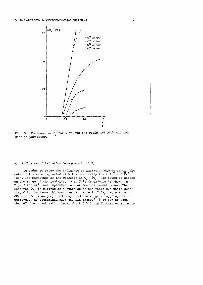
Fig. 3. Decrease in Tc for V versus the ratio R/d with the iondose as parameter.
a) Influence of Radiation Damage on T in V.c
In order to study the influence of radiation damage on Tc' themetal films were implanted with the chemically inert Ar+ and Kr+ions, The magnitude of the decrease in Tc' oTc ' was found to dependon the range of the implanted ions. This dependence is shown inFig. 3 for Ar+ ions implanted in V at four different doses. Theobserved OTc is plotted as a function of the ratio R/d where quantity d is the layer thickness andR = Rp + 1.17 6Rp ' Here Rp and6Rp are the mean projected range and the range straggling,respectively, as determined from the LSS theory(12~ It can be seenthat OTc has a saturation level for R/d ~ 1. In further experiments

20 O. MEYER, H. MANN, AND E. PHRILINGOS
Deerease in Telnormalized tothe bulk Tel versus ion dose fordifferent supereondueting materials.
Fig. 4
Ar'IN Nb, Sno Ar'IN Nbx Ar'IN Ta
Ar'IN Vv Ar'IN NbC, NbN
1,0
0.5
.//~.~~.
~/.--=====-: .0,1~:::::==-'-- f
J I , , I10" 10" 10" 10" 10"
ARGON DOSE [I0NS/CM',
7 .C .N.p
6Fig. 5
5 .5 Tc enhaneement in·s I Mo after implan-~4
.0 ting ions with~
I~ various numbers~ of valenee elee-3 .Se
trons per atom.
2
'Li .Bi
r r r r r r rNa Mg Mn Ag Zn AI CI ArCs Ga
O+-.---~,----.-----,----,-----,--+-------,---r-,~L-r--,--.-+--,---,--
o 2 3 4 5 6 7 8 9 10 1 2 3 4 5 6 7 8
NUMBER OF VALENCE ELECTRONS PER ATOM
where R exeeeds d by a faetor 3 to 4 it has been verified that thedeerease in Tc is due to the damage produeed and not due to ineorporated noble gas ions. The observed deerease in T for R/d < 1 isprobably due to enhaneed defeet diffusion during igplantation. Ifthis were not the ease the undamaged region of the metal layerwould provide an effeetive short eireuit. Defeets deeper than Rhave also been found in ion implanted V single erystals by use pof ehannelling teehnique and transmission eleetron mieroseopy(9).In all further damage experiments R/d was kept about 1 by suitableehoiee of ion energy.
The influenee of damage on Tc in different materials is sum-

ION IMPLANTATION IN SUPERCONDUCTING THIN FilMS 21
marized in Fig. 4 where OTc ' normalized to the corresponding Tc ofthe bulk material is presented as a function of argon ion dose.The effect of damage on the T of Nb3Sn layers was found to bestronger than that observed ig V and Nb. For example by the implantation of 10 16Ar+/cm 2 the initial T of 17.80 K was decreased to2.00 K. For a constant dose it can becseen that OTc/Tc increases formaterial with increasing electronic density of states at the Fermiedge. Vanadium is an exception as N(O) > N(O)Nb' NbC and NbN arefound to be highly radiation resistant~ No effects on Tc were observed by bombardment with protons and He+ ions at doses up to1016 ions/cm2 which is in agreement with results presented in (1).A possible impurity effect due to the implanted ions has been further investigated by implanting Ga+ ions in V and Nb. By comparison of OTc values for Kr+ implantation with those for Ga+ implantation, no additional effect could be detected (within the limitsof our measurement errors) with up to about 20 at % of Ga atomsincorporated in V and Nb films.
Since grain size is not affected by ion implantation as wasverified by thin film X-ray diffraction and since resistivity measurements show the mean free path of electrons at T > Tc is notstrongly reduced, it is assumed that the smearing out of structurein the electronic density of states is not the only factor in thedecrease of Tc by radiation damage. If this were true there shouldalso occur an increase in T for argon implanted Mo due to damage,but this is not observed. c
b) Chemical Effects of Implanted Ions
Possible chemical effects were studied by implanting ions fromnearly all groups of the periodic system in those transition metalswhere the damage effect is presumably low, i.e. where N(E) has nosharp peaks at the Fermi edge. In Fig. 5 the Tc enhancement observed by implanting ions with various values of valence electronsper atom in Mo layers is summarized. Tc enhancement up to 70 K wasobserved for implantation of elements from groups III(B), IV(C),V (N, P, Bi) and VI (S,O,Se).
For elements which are completely insoluble in Mo no Tc enhancement is observed. Those elements which form stable intermetalliccompounds, either superconducting or non-superconducting, give Tcenhancement. It is possible that the elements that tend to form intermetallic compounds stabilize the disorder in Mo on a microscopicscale, thereby producing the Tc enhancement. Preliminary results also show enhancement of T by implantation of N+ and S+ ions in WandRe. A summary of the res8lts obtained by ion implantation, T;I, intransition metals is given in TABLE I and are compared with the bulkvalue T~ulk, theoretical values for amorphous transition metals(14)Ta'heory , T~Q for vapor-quenched films (8) and T~P for "reactivelY"

22 O. MEYER, H. MANN, AND E. PHRILINGOS
Metal TBulk TTh{~M TVQ T
SP IrTc c c c c
Ti 0.39 0.5 - - ~ 1.2Zr 0.5 0.1-0.5 3.5 0 ~ 1. 2V 5.3 9 - ~5.3 2-3Nb 9.2 7.4-8.2 6 :S;9.2 3-5Ta 4.5 2.7-3.5 2 ~4.3 3-4Mo 0.9 9.6 8.5 7-8 "" 7W 0.01 4 -4.3 3.5 ,..4 I\t 3.5Re 1.7 6.2-7.5 7.5 ... 7 "" 4.5
Table I
Experimental (ionimplantation, vapour-quenching,sputtering) and theoretical results for Tcof some transitionmetals.
sputtered films (5,17). As the values of T21 are strongly dose dependent, maximum values were given for Tc enhancement, whereas forthe Tc decrease the values obtained for lOl6 Ar+/cm~ have beenused.
W0:::::>5<0::Wll.~W....Zo~iii~0::....
o S'IN Mo, N'IN Mo• C'lNMo
1018
DOSE (IONS/CM2)
Fig. 6
Dose dependenceof Tc enhancementafter implantingS+, N+ and C+ions in Mo.
No increase in Tc was found after implanting ions with low solubilities in Ti and Zr, whereas after implanting Fe+ ions in Tia Tc of about 30 K has been observed. This increase in Tc is probably due to the increase of the mumber of electrons per atom byimplanting soluble elements, an effect which will be studied

ION IMPLANTATION IN SUPERCONDUCTING THIN FILMS 23
further in more detail. Preliminary results on non transition metals (Al, Sn) show that implanting B+ and S+ increased the Tc ofAl to 2.SoK and of Sn to 4.4oK. Only a slight increase of aboutO.lo K has been observed by implanting Ar+ ions in Al under similarconditions. The dose dependence of the Tc enhancement is presented in Fig. 6 for S+, C+ and N+ ions implanted in Mo. A maximumvalue in T is observed. T~ax increases with decreasing mass ofimplanted tons and shifts to higher doses. These maxima werefound to occur for lower ion doses in Re and for higher dosesin W as compared with the results presented for Mo. More detailedstudies especially on the density changes in the implanted layers
..... 7i'~
w 60:::::J
!<! 50::Wa..
"~Wl-
Z 30;::Vi 2z<i0::l-
• C+ in Mo
iJ. C' in Mo .7'1016 Ar'/Cm2
x N' in Moo S' in Mo
Fig. 7Influence of an isochronal anneal process on Tc of implanted Mo layers.
200 "00 600 800
ANNEAL TEMPERATURE ['e J
....J 8 '103
WZz<i:r:un::wa..
~ "'103
Z:::JoU
3 '1017 N;/cm2 (50 10 130 KeVI in Mo layer
- UNIMPLANTED
" .900·C ANNEAL
o AS IMPLANTED
" ·800·C ANNEAL
" • 900' C ANNEAL
660Äf-------i
CHANNEL NUMBER
Fig. 8Backscattering spectrafrom implanted andunimplanted Mo layers at room temperature and at 8000 Cand 900oC.

24 O. MEYER, H. MANN, AND E. PHRllINGOS
are neeessary and will be done in the future.
e) Annealing Effeets
Isoehronal annealing processes in a vaeuum of 10-7 Torr havebeen performed on implanted Mo layers and the dependenee of Tc onannealing temperature is shown in Fig. 7. The Tc enhaneement isfound to be stable for annealing temperatures up to 4000 C in S+implanted layers and up to 8000 e in e+ and N+ implanted layers.The influenee of lattiee disorder was studied by additional implanting 7 x 10 16 Ar+/em2 in a e+ implanted Mo layer with a Tc of7.2oK. The observed Tc reduetion of O.SoK as shown in Fig. 7 is smalleompared to results presented in Fig. 4. From the baekseatteringspeetra taken from implanted Mo layers and unimplanted layers itean be seen (Fig. 8) that at 8000 e the nitrogen has moved throughout the metal layer. At 900
0 e additional oxygen has been ineorporated as ean be seen in the speetra of the unimplanted layer andthe inhomogeneities visible in the speetra of the implanted layerseem to indieate the formation of preeipitations. The inerease ofTc due to V3Si formation(13)has prevented study of the effeet ofanneal temperature on implanted V layers. In the ease of the Nb3Snfilms,however, the influenee on Tc due to radiation damage has beenfound to be removed on annealing for several hours at 800oe.
DIseUSSION
To summarize, we found a strong deerease of the transitiontemperature of Ta, V, Nb, and Nb3Sn films after bombarding withlow energy high mass ions. The magnitude of the deerease in Tc wasfound to depend on mass, dose and range of implanted ions, and istherefore attributed to the radiation damage produeed during implantation and not to ehemieal effeets. It is assumed that thesmearing out of struetures in the eleetronie state density distribution is only one reason for the observed deerease in Tc'Otherwise, argon implantation in W, Mo and Re should produee aTc inerease for the same reason, but this is not observed. Thedisturbanee of the long range order in Nb3Sn may explain thestrong deerease of T found for that material.
e
T enhaneement was observed by implanting seleeted ions ableto forg intermetallic eompounds but otherwise of low solubility inMo, W, and Re films. It is assumed that these ions do not stabilizea high Tc phase after implantation but ean stabilize a disloeationof the lattiee atoms. The suggestioEthat implantation of impuritieswill stabilize high Tphases largely eomposed of the element inquestion,as was obser~ed in transition metal films evaporated in avaeuum of 10- 5 to 10- 6 Torr (4) or sputtered in the presenee ofgaseous impurities (5),ean be diseussed as follows:In eontrast to results given in (4) our layers had bulk T 's in
e

ION IMPLANTATION IN SUPERCONDUCTING THIN FILMS 25
the limit of measurement (T > 1.2oK). X-ray patternsof unimplantedNb and Mo films did only sh8w-the normal bcc phase. The implantedregions of these layers did not show any difference in the X-raypattern. There was no evidence for the presence of other phasesand there was no spread in the line width indicating small grainsizes. In addition the implanted Mo layers with high Tc were stableagainst irradiation with argon ions and stable against temperaturetreatment. In forming an impurity stabilized high Tc-phase onewould also expect a saturation in the dose dependence of Tratherthan a maximum. c
There are several arguments against the suggestion that thehigh Tc phases of MoN and MoC have formed during implantation.Firstly, the dose for maximum Tc enhancement was lower than necessary for the formation of stoichiometric MoN and MoC, secondly N+ inW increased Tc but no high Tc WN-phase is known. N+ in Ti and Zrdid not increase Tc but TiN as well as ZrN are known to be superconducting.
The stabilized dislocation mentioned above may change the atomic volume(14) and therefore the electron density which causes ashift in the density of states at the Fermi edge. A further possiblereason for this shift may be found in the high electrcnegativityof the implanted ions causing a Tc increase. The observed maxima inthe dose dependence of Tc and the shift in the maxima for differentmaterial may be explained with the assumption that the Fermi energyis shifted across a peak in N(E) resulting in a maximum in Tc' Theobserved increase or decrease in T may also be discussed in termsof the Eliasberg function a 2 (w) F(~) (15) which describes the interaction between phonons and electrons causing the effective attraction between the electrons in a superconductor. It has beenshown for nontransition metals(16) that the softening of the phonondistribution and therefore of a 2F',(w), in highly disordered superconductors can result in either a positive or a negative change inthe transition temperature. In this regard the observed decreasein Tc for the group Vb elements may be due to a decrease in a ordue to a shift of F(w) to higher frequencies.
Further, by implanting ions of higher solubility in the hostlattice it is possible to change the number of electrons per atomand to increase T in suitable ion - target systems.
c
ACKNOWLEDGEMENT
Thanks are due to M. Kraatz and R. Smithey for careful layerpreparation and ion implantation and to F. Ratzel for performingT measurements. We further want to thank W. Buckel, J. Geerk,M~ Gettings and G. Linker for many helpful discussions.
26 O. MEYER, H. MANN, AND E. PHRILINGOS
REFERENCES
(1) G.W. CULLEN in BNL-50155 (1968) p. 437.
(2) W. BUCKEL and R.J. HILSCH, z. Phys. 132, 420 (1952);138, 109 (1954).
(3) Review of M. STRONGIN Physica Vol. 55, 155 (1971).
(4) W.L. BOND et al., Phys. Rev. Lett. ~, 260 (1965).
(5) K.L. CHOPRA, M.R. RANDLETT, and R.H. DUFF, Phil. mag. 16,261 (1971).
(6) R.C. DYNES, Solid State Communications, lQ, 615 (1972).
(7) J.W. GARLAND, K.H. BENNEMANN and F.M. MUELLER, Phys. Rev.Letters 21, 1315 (1968) .
(8) M.M. COLLVER, R.H. HAMMOND, Phys. Rev. Letters 30,92 (1973).
(9) M. GETTINGS, G. LINKER and O. MEYER, 111. Int. Conf. on IonImplantation, New York, Dec. 11-14, 1972.
(10) O. MEYER, G. LINKER and B. KRAEFT, Int. Conf. on Ion BeamSurface Layer Analysis, Yorktown Heights, New York, June18-20, (1973).
(11) G. LINKER, O. MEYER and M. GETTINGS, Int. Conf. on Ion BeamSurface Layer Analysis. Yorktown Heights, New York, June18-20, (1973).
(12) J. LINDHARD, H.E. SCHI~TT, and M. SCHARFF, Mat. Phys. Med. 332 (1963).
(13) F.J. CADIEU, in AlT Conf. Proc. No. 4, 213 (1972), ed. byD.H. Douglass.
(14) K.H. BENNEMANN, winter Colloquium in Schleching 19.2-23.2.(1973) .
(15) J.R. SCHRIEFFER, Theory of Superconductivity, Benjamin Inc.Publ. N.Y. 1964.
(16) G. BERGMANN and D. RAINER, z. Physik 263, 59 (1973).
(17) D. GERSTENBERG, P.M. HALL, J. Electrochem. Soc. lll,936 (1964).
PRINTED IN U.S.,