Embed Size (px)
Citation preview
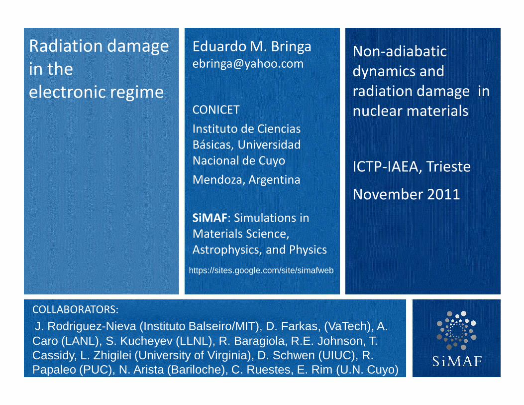
COLLABORATORS:
J. Rodriguez-Nieva (Instituto Balseiro/MIT), D. Farkas, (VaTech), A. Caro (LANL), S. Kucheyev (LLNL), R. Baragiola, R.E. Johnson, T. Cassidy, L. Zhigilei (University of Virginia), D. Schwen (UIUC), R. Papaleo (PUC), N. Arista (Bariloche), C. Ruestes, E. Rim (U.N. Cuyo)
Non-adiabatic
dynamics and
radiation damage in
nuclear materials
ICTP-IAEA, Trieste
November 2011
Eduardo M. [email protected]
CONICET
Instituto de Ciencias
Básicas, Universidad
Nacional de Cuyo
Mendoza, Argentina
SiMAF: Simulations in
Materials Science,
Astrophysics, and Physics
Radiation damage
in the
electronic regime
https://sites.google.com/site/simafweb

MENDOZA, LAND OF THE SUN AND THE GOOD WINE
Malbec
Top 2 harvest festival
(Nat Geo 2011)
• Background and Introduction
– Track models
• Molecular Dynamics (MD) of damage in the electronic regime
– Thermal Spikes, Two Temperature Models and Coulomb Explosions.
• Examples
– Electronic sputtering, track formation: defects, phase change,
craters & bumps.
• Conclusions and future outlook
OUTLINE
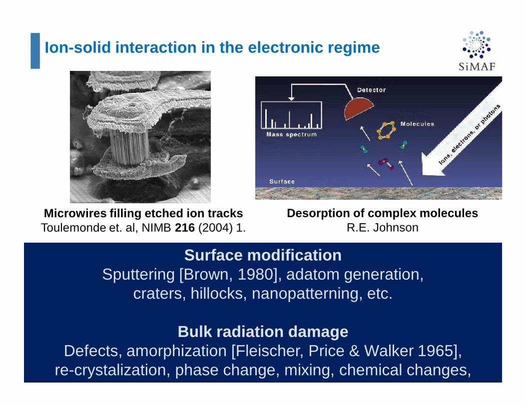
Ion-solid interaction in the electronic regime
Surface modificationSputtering [Brown, 1980], adatom generation,
craters, hillocks, nanopatterning, etc.
Bulk radiation damageDefects, amorphization [Fleischer, Price & Walker 1965],
re-crystalization, phase change, mixing, chemical changes, compaction, changes in mechanical/optical properties, etc.
Microwires filling etched ion tracksToulemonde et. al, NIMB 216 (2004) 1.
Desorption of complex moleculesR.E. Johnson
Energy (keV)
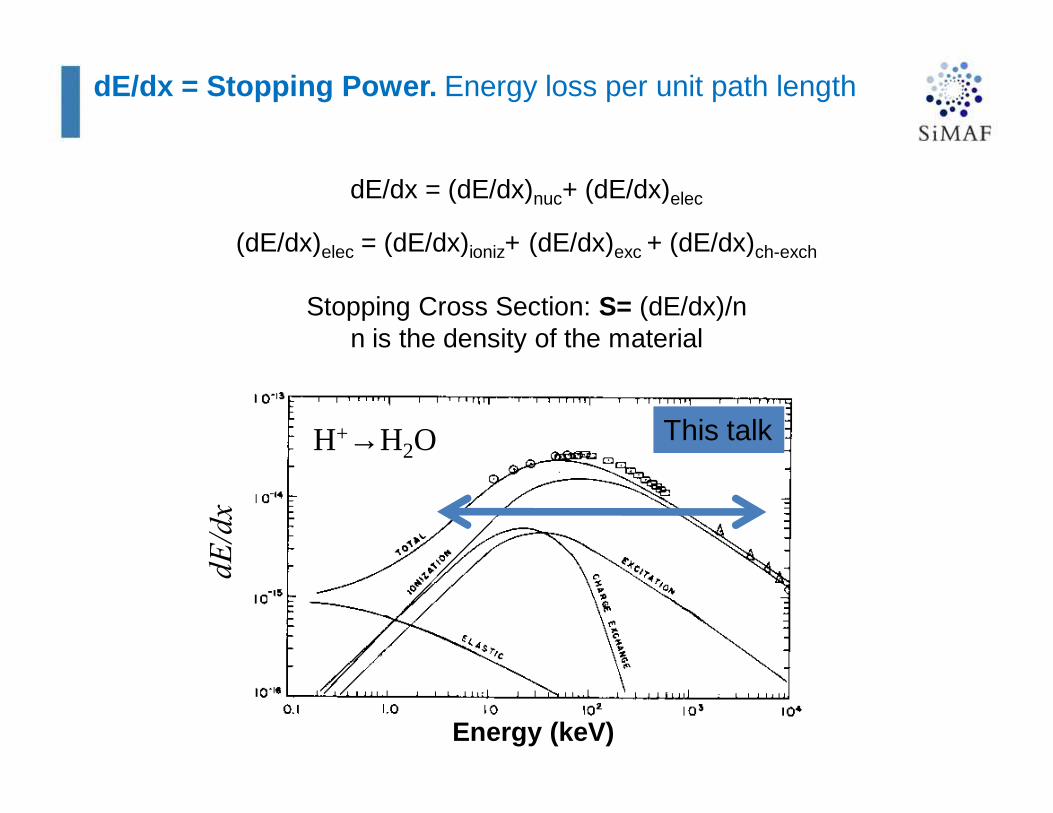
dE/dx = Stopping Power. Energy loss per unit path length
dE/dx = (dE/dx)nuc+ (dE/dx)elec
(dE/dx)elec = (dE/dx)ioniz+ (dE/dx)exc + (dE/dx)ch-exch
Stopping Cross Section: S= (dE/dx)/nn is the density of the material
H+→H2O This talk
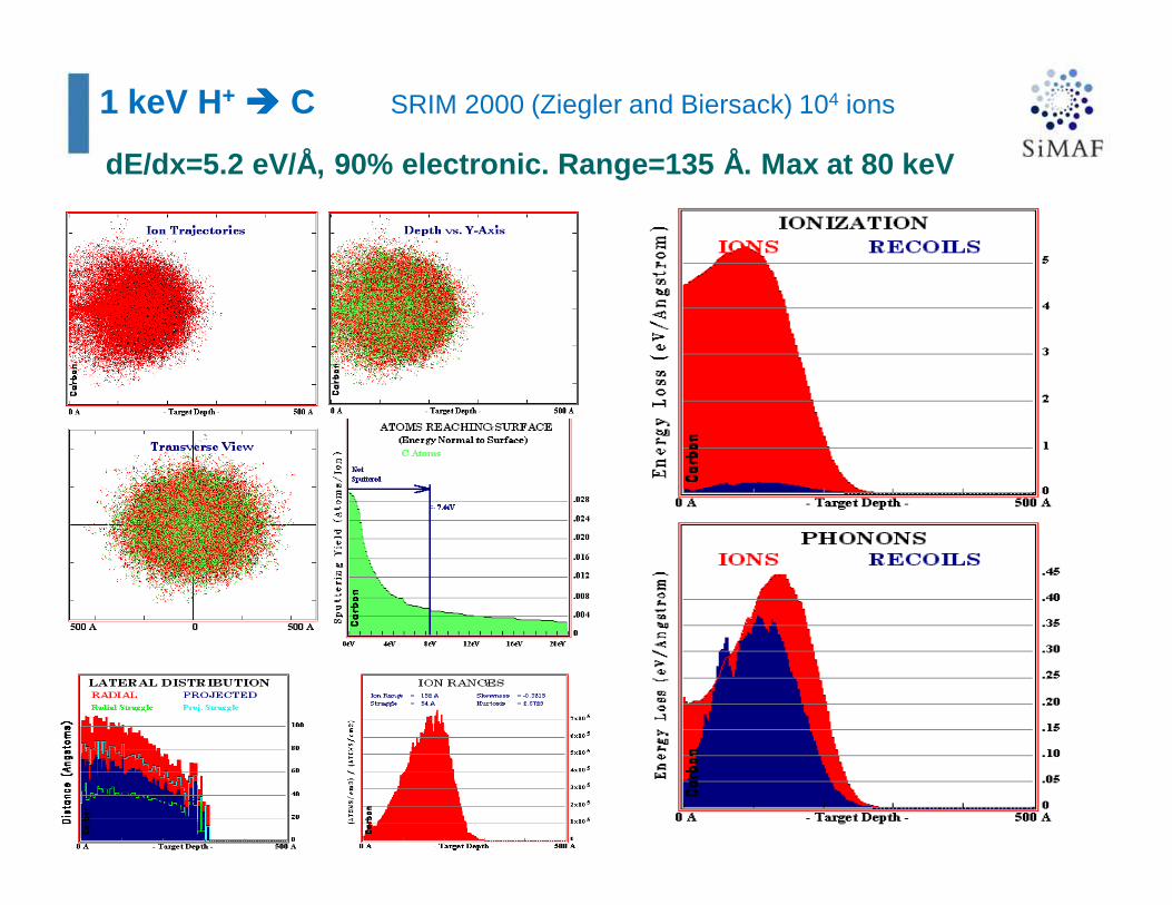
1 keV H+ ���� C SRIM 2000 (Ziegler and Biersack) 104 ions
dE/dx=5.2 eV/Å, 90% electronic. Range=135 Å. Max at 80 keV
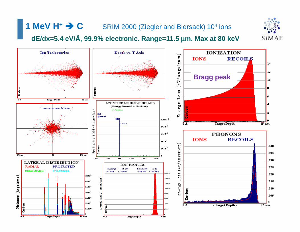
1 MeV H+ ���� C SRIM 2000 (Ziegler and Biersack) 104 ions
dE/dx=5.4 eV/Å, 99.9% electronic. Range=11.5 µµµµm. Max at 80 keV
Bragg peak
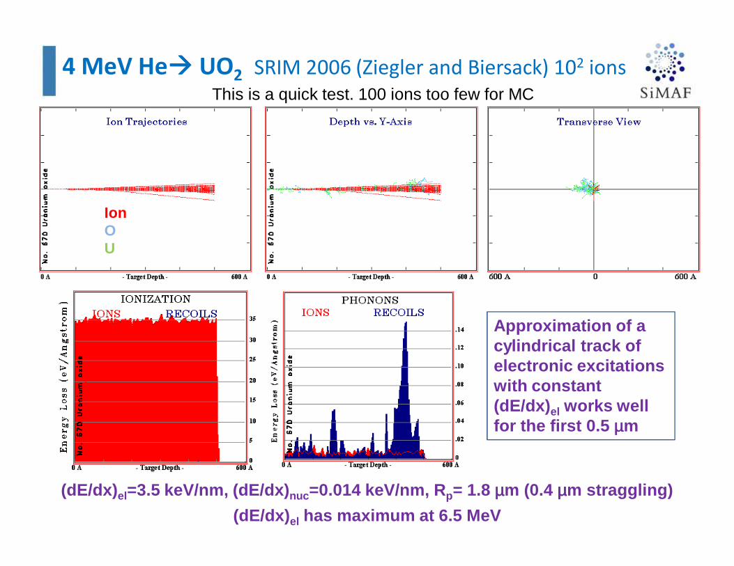
4 MeV He���� UO2 SRIM 2006 (Ziegler and Biersack) 102 ions
(dE/dx) el=3.5 keV/nm, (dE/dx) nuc=0.014 keV/nm, R p= 1.8 µµµµm (0.4 µµµµm straggling)
(dE/dx) el has maximum at 6.5 MeV
Approximation of a cylindrical track of electronic excitations with constant (dE/dx) el works well for the first 0.5 µµµµm
IonOU
This is a quick test. 100 ions too few for MC
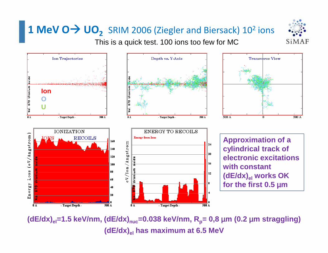
1 MeV O���� UO2 SRIM 2006 (Ziegler and Biersack) 102 ions
(dE/dx) el=1.5 keV/nm, (dE/dx) nuc=0.038 keV/nm, R p= 0,8 µµµµm (0.2 µµµµm straggling)
(dE/dx) el has maximum at 6.5 MeV
Approximation of a cylindrical track of electronic excitations with constant (dE/dx) el works OK for the first 0.5 µµµµm
IonOU
This is a quick test. 100 ions too few for MC
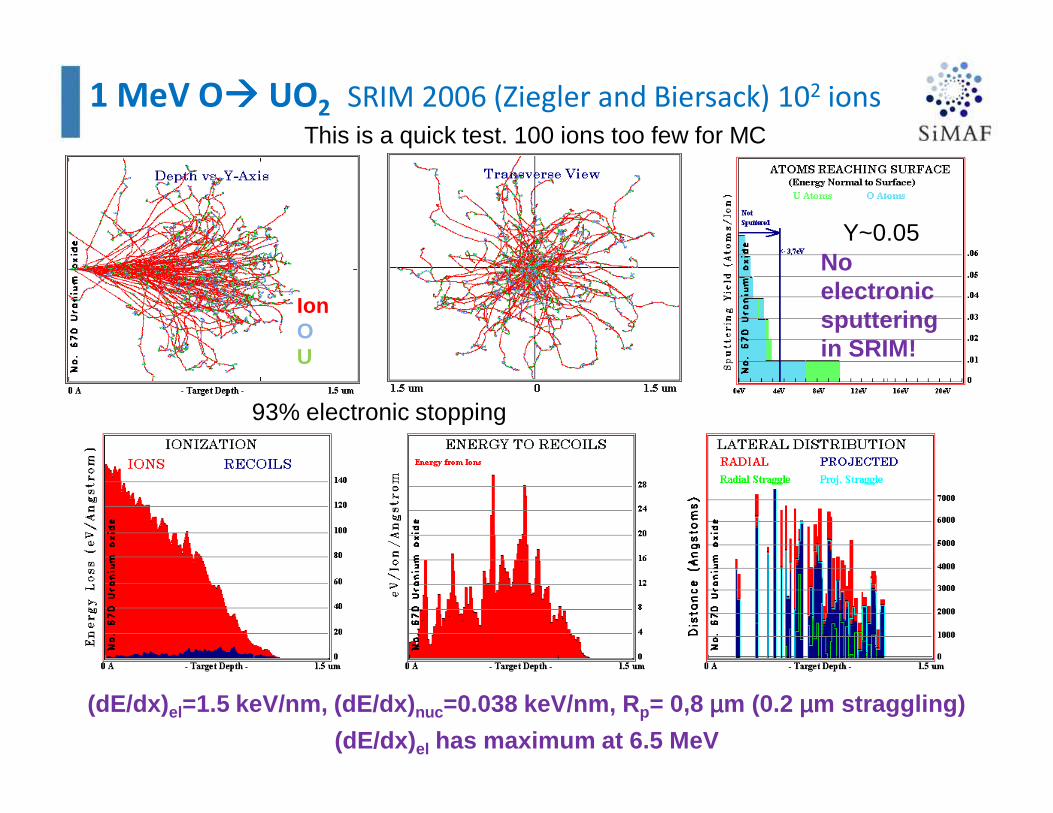
1 MeV O���� UO2 SRIM 2006 (Ziegler and Biersack) 102 ions
(dE/dx) el=1.5 keV/nm, (dE/dx) nuc=0.038 keV/nm, R p= 0,8 µµµµm (0.2 µµµµm straggling)
(dE/dx) el has maximum at 6.5 MeV
Y~0.05
93% electronic stopping
No electronic sputtering in SRIM!
IonOU
This is a quick test. 100 ions too few for MC

Ion Range, or where does an ion stop?
R =∫ |dE/dx|-1 dE
Rp
R⊥
Rp = Projected Range
R⊥ = Perpendicular Range
Stopping and Rangehave statistical fluctuations!!!Sometimes the largest fluctuations may determine the final outcome
WARNING!!
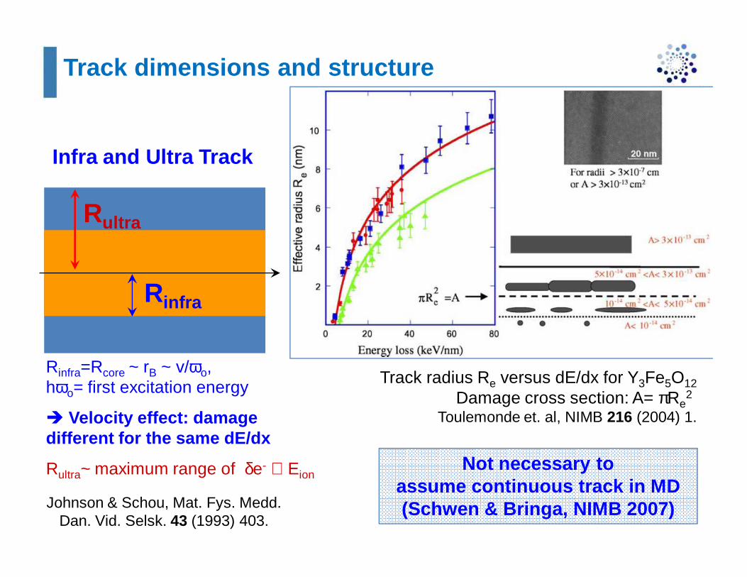
Track dimensions and structure
Rultra
Rinfra
Rinfra=Rcore ~ rB ~ v/ωo, hωo= first excitation energy
� Velocity effect: damage different for the same dE/dx
Rultra~ maximum range of δe- ∝ Eion
Infra and Ultra Track
Track radius Re versus dE/dx for Y3Fe5O12Damage cross section: A= πRe
2
Toulemonde et. al, NIMB 216 (2004) 1.
Johnson & Schou, Mat. Fys. Medd. Dan. Vid. Selsk. 43 (1993) 403.
Not necessary toassume continuous track in MD (Schwen & Bringa, NIMB 2007)
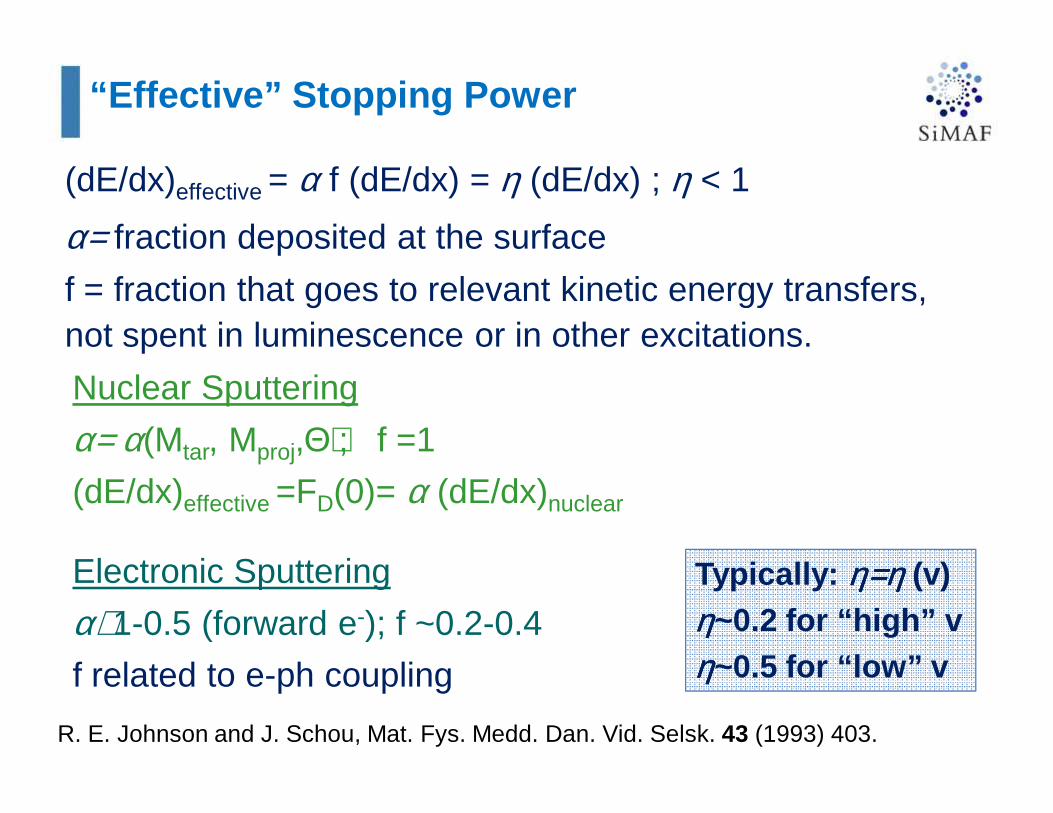
“Effective” Stopping Power
(dE/dx)effective = α f (dE/dx) = η (dE/dx) ; η < 1
α= fraction deposited at the surface
f = fraction that goes to relevant kinetic energy transfers, not spent in luminescence or in other excitations.
Nuclear Sputtering
α= α(Mtar, Mproj,Θ) ; f =1
(dE/dx)effective =FD(0)= α (dE/dx)nuclear
Electronic Sputtering
α∼1-0.5 (forward e-); f ~0.2-0.4
f related to e-ph coupling
R. E. Johnson and J. Schou, Mat. Fys. Medd. Dan. Vid. Selsk. 43 (1993) 403.
Typically: η=η η=η η=η η=η (v)ηηηη~0.2 for “high” vηηηη~0.5 for “low” v
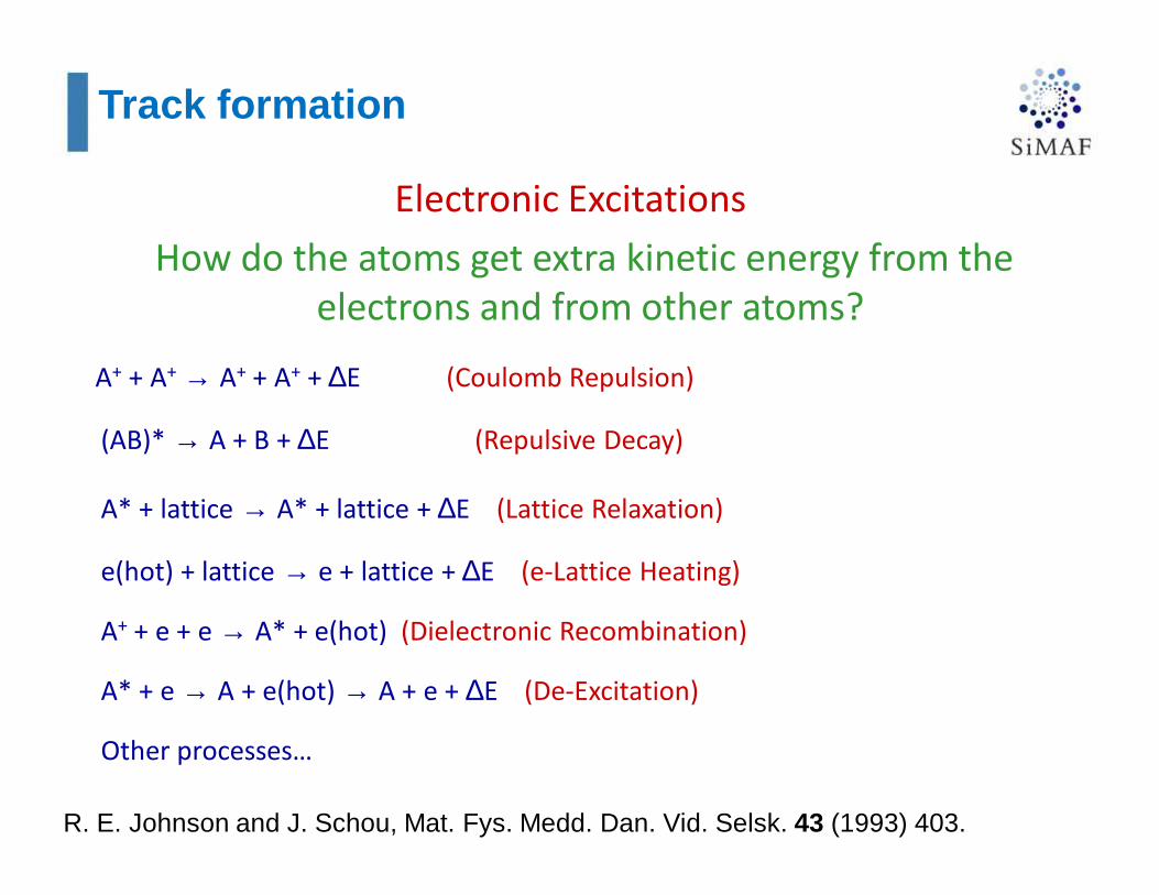
Track formation
Electronic Excitations
How do the atoms get extra kinetic energy from the
electrons and from other atoms?
A+ + A+ → A+ + A+ + ∆E (Coulomb Repulsion)
(AB)* → A + B + ∆E (Repulsive Decay)
A* + lattice → A* + lattice + ∆E (Lattice Relaxation)
e(hot) + lattice → e + lattice + ∆E (e-Lattice Heating)
A+ + e + e → A* + e(hot) (Dielectronic Recombination)
A* + e → A + e(hot) → A + e + ∆E (De-Excitation)
Other processes…
R. E. Johnson and J. Schou, Mat. Fys. Medd. Dan. Vid. Selsk. 43 (1993) 403.
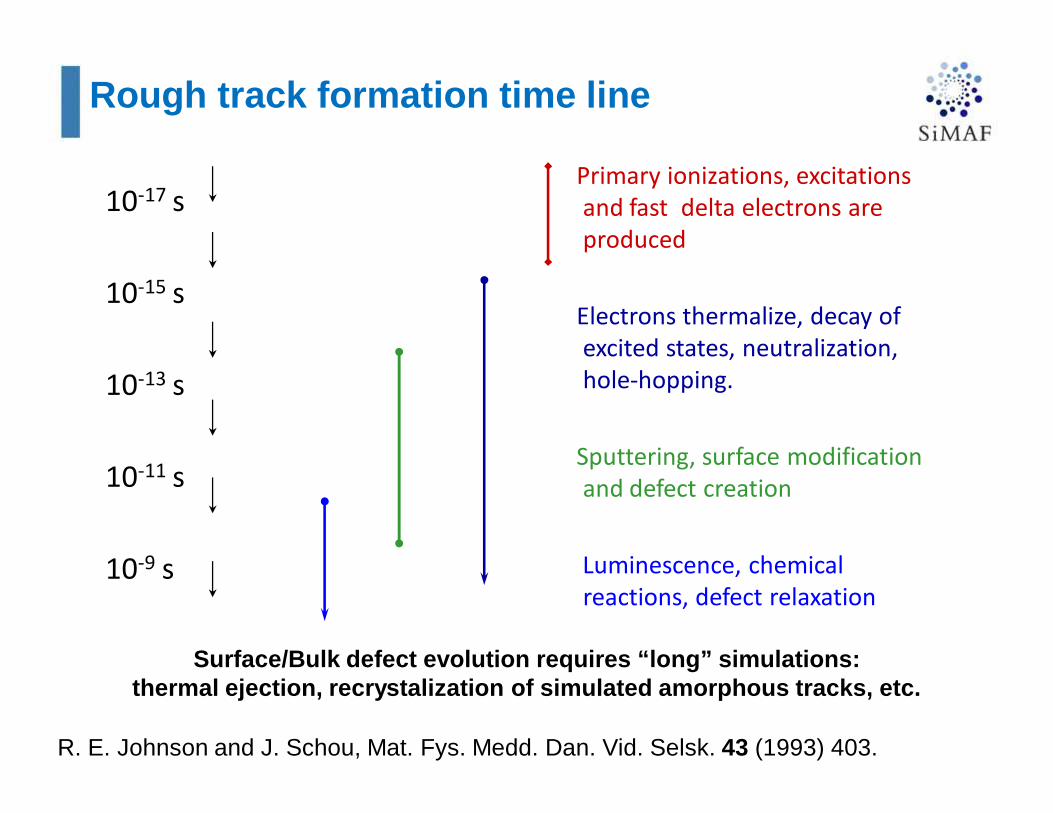
Rough track formation time line
10-17 s
10-15 s
10-13 s
10-11 s
10-9 s
Primary ionizations, excitations
and fast delta electrons are
produced
Electrons thermalize, decay of
excited states, neutralization,
hole-hopping.
Sputtering, surface modification
and defect creation
Luminescence, chemical
reactions, defect relaxation
R. E. Johnson and J. Schou, Mat. Fys. Medd. Dan. Vid. Selsk. 43 (1993) 403.
Surface/Bulk defect evolution requires “long” simul ations: thermal ejection, recrystalization of simulated amor phous tracks, etc.
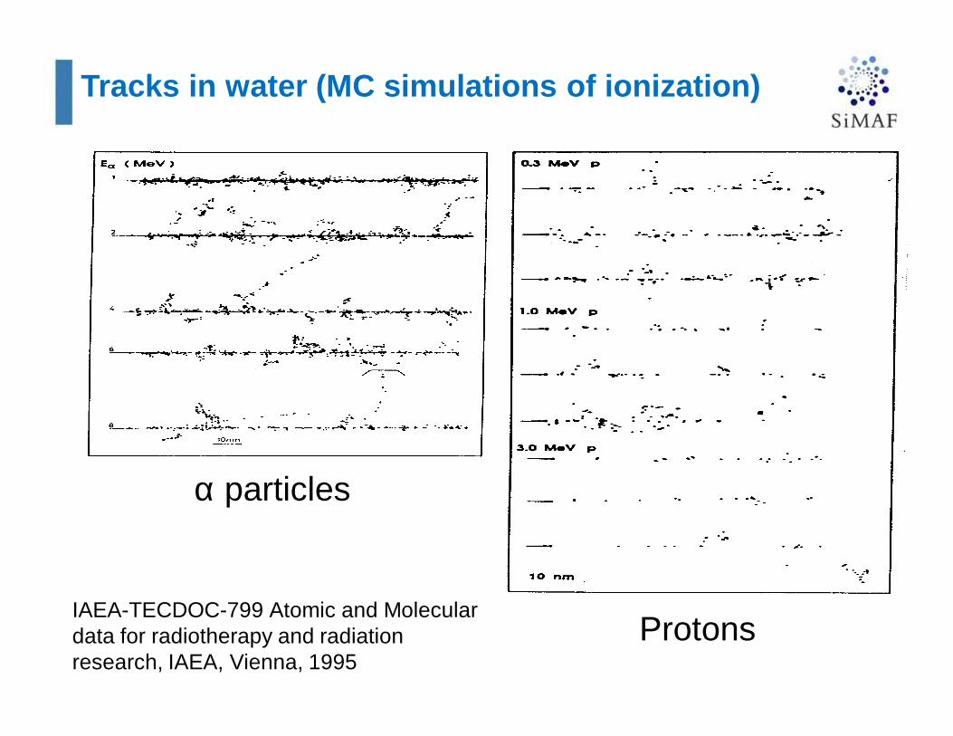
Tracks in water (MC simulations of ionization)
α particles
ProtonsIAEA-TECDOC-799 Atomic and Molecular data for radiotherapy and radiation research, IAEA, Vienna, 1995
FAST ION
H2O
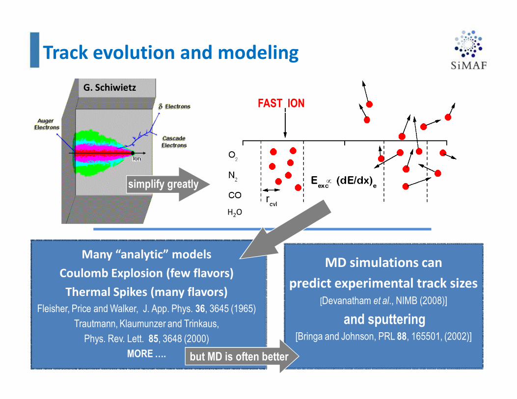
Track evolution and modeling
Many “analytic” models
Coulomb Explosion (few flavors)
Thermal Spikes (many flavors)
Fleisher, Price and Walker, J. App. Phys. 36, 3645 (1965)
Trautmann, Klaumunzer and Trinkaus,
Phys. Rev. Lett. 85, 3648 (2000)
MORE ….
MD simulations can
predict experimental track sizes
[Devanatham et al., NIMB (2008)]
and sputtering[Bringa and Johnson, PRL 88, 165501, (2002)]
G. Schiwietz
simplify greatly
but MD is often better
• Background and Introduction
– Track models
• Molecular Dynamics (MD) of damage in the electronic regime
– Thermal Spikes, Two Temperature Models and Coulomb Explosions.
• Examples
– Electronic sputtering,track formation: defects, phase change,
craters & bumps.
• Conclusions and future outlook
OUTLINE
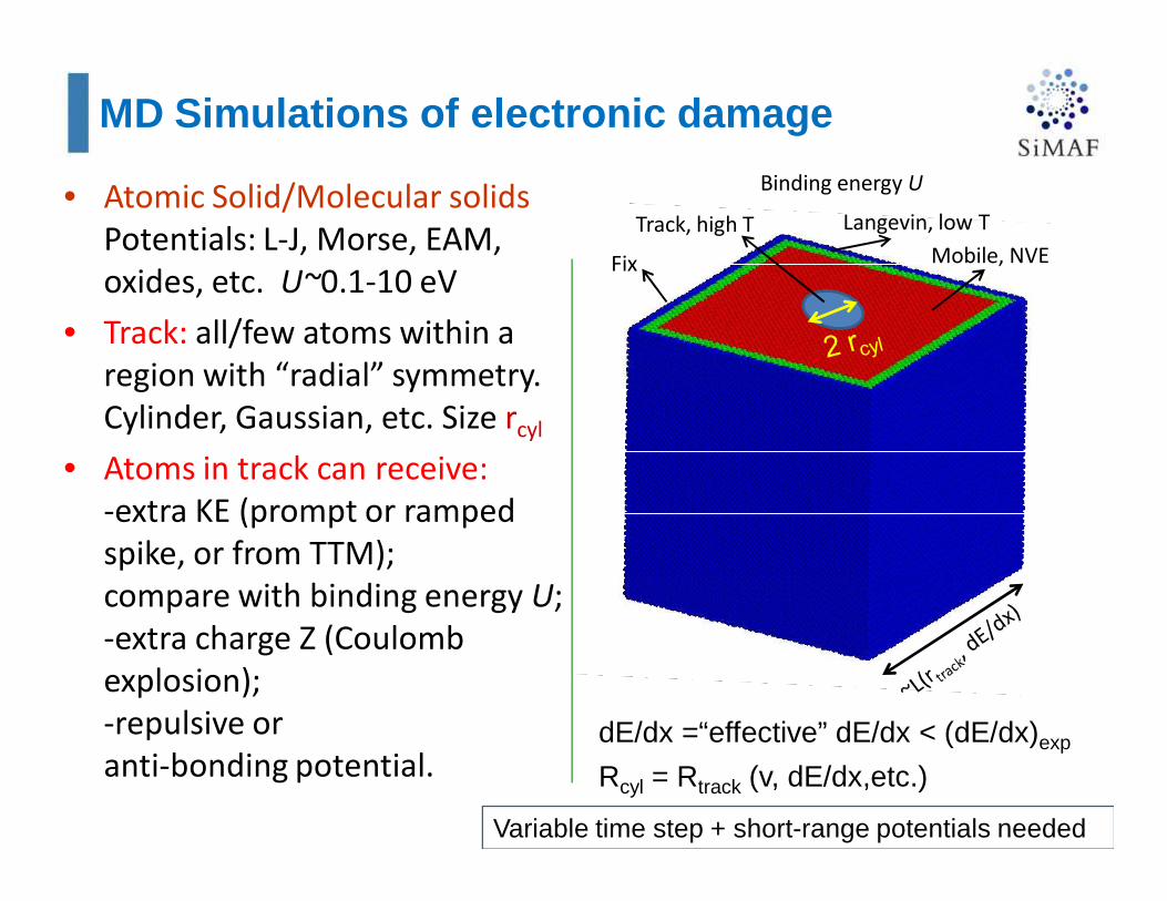
MD Simulations of electronic damage
• Atomic Solid/Molecular solids
Potentials: L-J, Morse, EAM,
oxides, etc. U~0.1-10 eV
• Track: all/few atoms within a
region with “radial” symmetry.
Cylinder, Gaussian, etc. Size rcyl
• Atoms in track can receive:
-extra KE (prompt or ramped
spike, or from TTM);
compare with binding energy U;
-extra charge Z (Coulomb
explosion);
-repulsive or
anti-bonding potential.
Fix
Langevin, low T
Mobile, NVE
Track, high T
dE/dx =“effective” dE/dx < (dE/dx)exp
Rcyl = Rtrack (v, dE/dx,etc.)
Variable time step + short-range potentials needed
Binding energy U
MD simulation of electronic damage -II
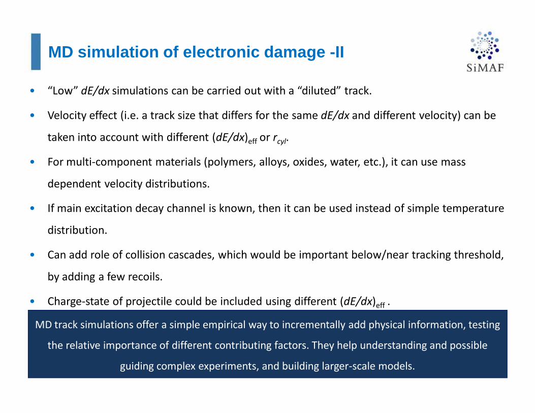
• “Low” dE/dx simulations can be carried out with a “diluted” track.
• Velocity effect (i.e. a track size that differs for the same dE/dx and different velocity) can be
taken into account with different (dE/dx)eff or rcyl.
• For multi-component materials (polymers, alloys, oxides, water, etc.), it can use mass
dependent velocity distributions.
• If main excitation decay channel is known, then it can be used instead of simple temperature
distribution.
• Can add role of collision cascades, which would be important below/near tracking threshold,
by adding a few recoils.
• Charge-state of projectile could be included using different (dE/dx)eff .
MD track simulations offer a simple empirical way to incrementally add physical information, testing
the relative importance of different contributing factors. They help understanding and possible
guiding complex experiments, and building larger-scale models.
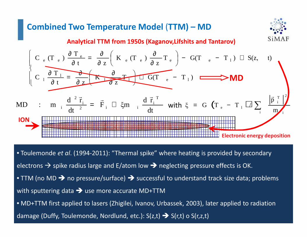
−+
∂∂
∂∂=
∂∂
+−−
∂∂
∂∂=
∂∂
)TG(TTz
Kzt
TC
t)S(z,)TG(TTz
)(TKzt
T)(TC
lelll
l
leeeee
ee
( ) ∑−=i i
2Ti
le m
p/TTGξ
r
with
Combined Two Temperature Model (TTM) – MD
MD
dt
rdξmF
dt
rdm :MD
Ti
ii2i
2
i
rr
r
+=
ION
Electronic energy deposition
• Toulemonde et al. (1994-2011): “Thermal spike” where heating is provided by secondary
electrons � spike radius large and E/atom low � neglecting pressure effects is OK.
• TTM (no MD � no pressure/surface) � successful to understand track size data; problems
with sputtering data � use more accurate MD+TTM
• MD+TTM first applied to lasers (Zhigilei, Ivanov, Urbassek, 2003), later applied to radiation
damage (Duffy, Toulemonde, Nordlund, etc.): S(z,t) � S(r,t) o S(r,z,t)
Analytical TTM from 1950s (Kaganov,Lifshits and Tantarov)
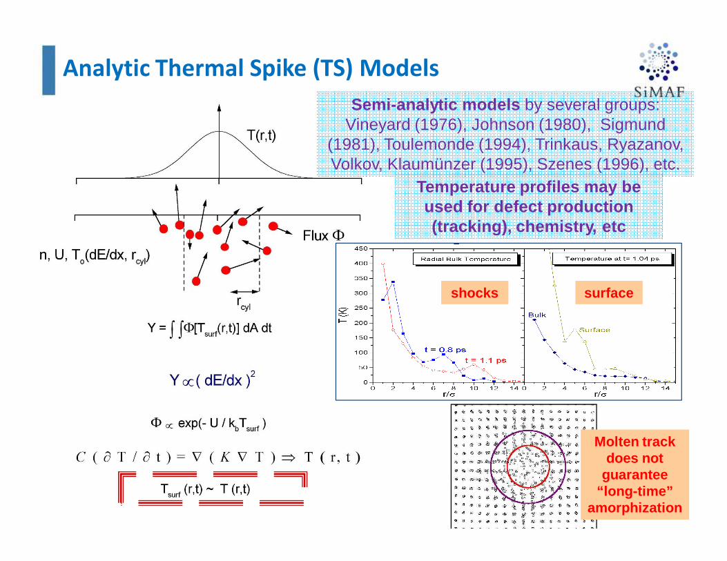
Analytic Thermal Spike (TS) Models
Temperature profiles may be used for defect production (tracking), chemistry, etc
Semi-analytic models by several groups: Vineyard (1976), Johnson (1980), Sigmund
(1981), Toulemonde (1994), Trinkaus, Ryazanov, Volkov, Klaumünzer (1995), Szenes (1996), etc.
shocks surface
Molten track does not
guarantee “long-time”
amorphization
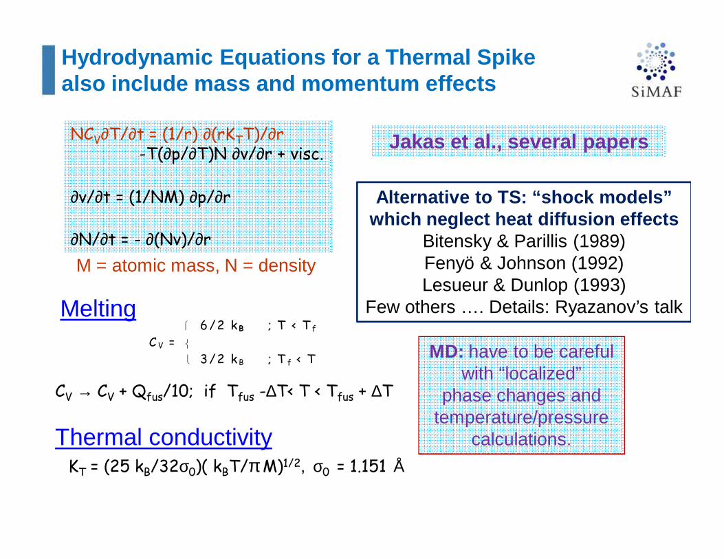
Hydrodynamic Equations for a Thermal Spike also include mass and momentum effects
M = atomic mass, N = density
6 /2 k B ; T < T f
C V =
3 /2 k B ; T f < T
Melting
Thermal conductivityKT = (25 kB/32σ0)( kBT/π M)1/2, σ0 = 1.151 Å
NCV∂T/∂t = (1/r) ∂(rKTT)/∂r-T(∂p/∂T)N ∂v/∂r + visc.
∂v/∂t = (1/NM) ∂p/∂r
∂N/∂t = - ∂(Nv)/∂r
CV → CV + Qfus/10; if Tfus -∆T< T < Tfus + ∆T
Jakas et al., several papers
Alternative to TS: “shock models” which neglect heat diffusion effects
Bitensky & Parillis (1989) Fenyö & Johnson (1992)Lesueur & Dunlop (1993)
Few others …. Details: Ryazanov’s talk
MD: have to be careful with “localized”
phase changes and temperature/pressure
calculations.
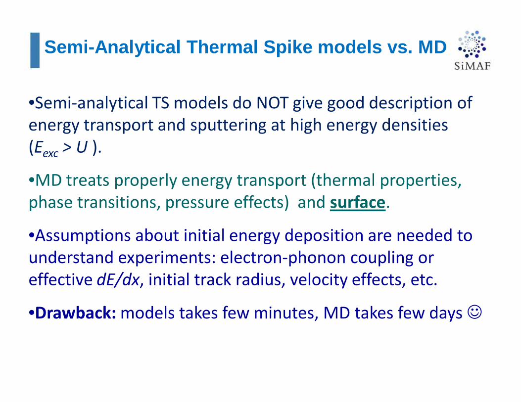
Semi-Analytical Thermal Spike models vs. MD
•Semi-analytical TS models do NOT give good description of
energy transport and sputtering at high energy densities
(Eexc > U ).
•MD treats properly energy transport (thermal properties,
phase transitions, pressure effects) and surface.
•Assumptions about initial energy deposition are needed to
understand experiments: electron-phonon coupling or
effective dE/dx, initial track radius, velocity effects, etc.
•Drawback: models takes few minutes, MD takes few days ☺
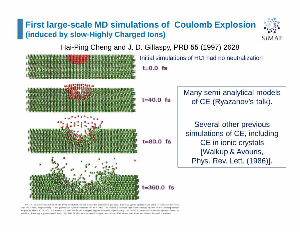
First large-scale MD simulations of Coulomb Explos ion (induced by slow-Highly Charged Ions)
Hai-Ping Cheng and J. D. Gillaspy, PRB 55 (1997) 2628
Many semi-analytical models of CE (Ryazanov’s talk).
Several other previous simulations of CE, including
CE in ionic crystals [Walkup & Avouris,
Phys. Rev. Lett. (1986)].
Initial simulations of HCI had no neutralization
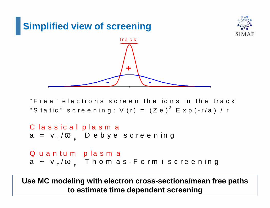
Simplified view of screeningt r a c k
" F r e e " e l e c t r o n s s c r e e n t h e i o n s i n t h e t r a c k
" S t a t i c " s c r e e n i n g : V ( r ) = ( Z e ) 2 E x p ( - r / a ) / r
C l a s s i c a l p l a s m aa = v T / ω p D e b y e s c r e e n i n g
Q u a n t u m p l a s m a a ~ v F / ω p T h o m a s - F e r m i s c r e e n i n g
--
+
Use MC modeling with electron cross- sections/mean free paths to estimate time dependent screening
∝
PE~(Nche)2/d ∆KE
Y (dJ/dx)2
dJ/dx= A (Zeff/v)2 ln(B v2)
+
+
+
+
+ +
+
+
+
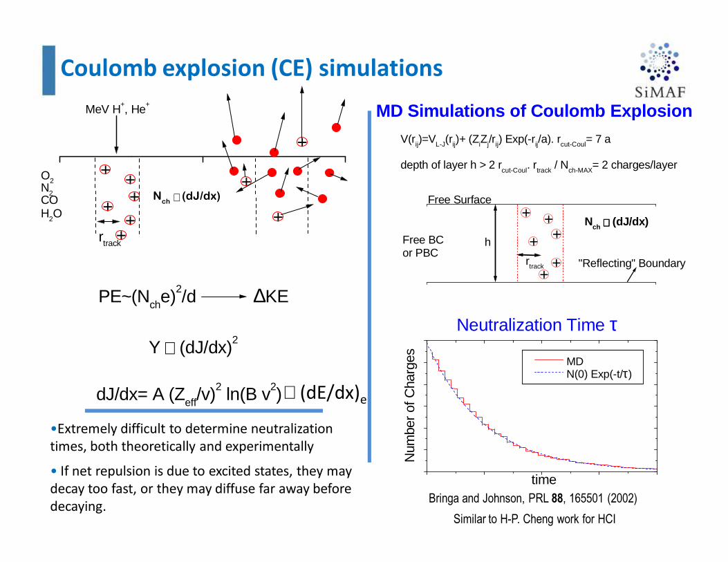
O2N2COH2O
MeV H+, He+
rtrack
∝Nch (dJ/dx)
∝ (dE/dx)e
h
"Reflecting" Boundary
Free BCor PBC
Free Surface
rtrack ++
++
+
+
Neutralization Time τ
V(rij)=VL-J(rij)+ (ZiZj/rij) Exp(-rij/a). rcut-Coul= 7 a
depth of layer h > 2 rcut-Coul
. rtrack
/ Nch-MAX
= 2 charges/layer
MD Simulations of Coulomb Explosion
∝∝∝∝Nch (dJ/dx)
MD N(0) Exp(-t/τ)
Num
ber
of C
harg
es
time
Similar to H-P. Cheng work for HCI
•Extremely difficult to determine neutralization
times, both theoretically and experimentally
• If net repulsion is due to excited states, they may
decay too fast, or they may diffuse far away before
decaying.
Coulomb explosion (CE) simulations
Bringa and Johnson, PRL 88, 165501 (2002)
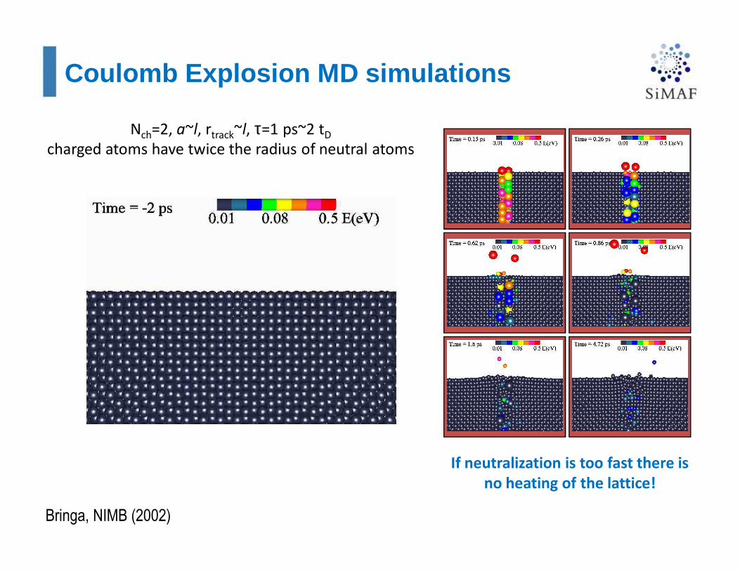
Coulomb Explosion MD simulations
Nch=2, a~l, rtrack~l, τ=1 ps~2 tD
charged atoms have twice the radius of neutral atoms
If neutralization is too fast there is
no heating of the lattice!
Bringa, NIMB (2002)
0.1 1 100.01
0.1
1
10
E
-2
2nd layer 1st layer
(a) Coulomb, τ ≈ τD
(b) Coulomb, τ ≈ 20 τD
(c) Thermal Spike
(dY
/dE
)/Y
E/U
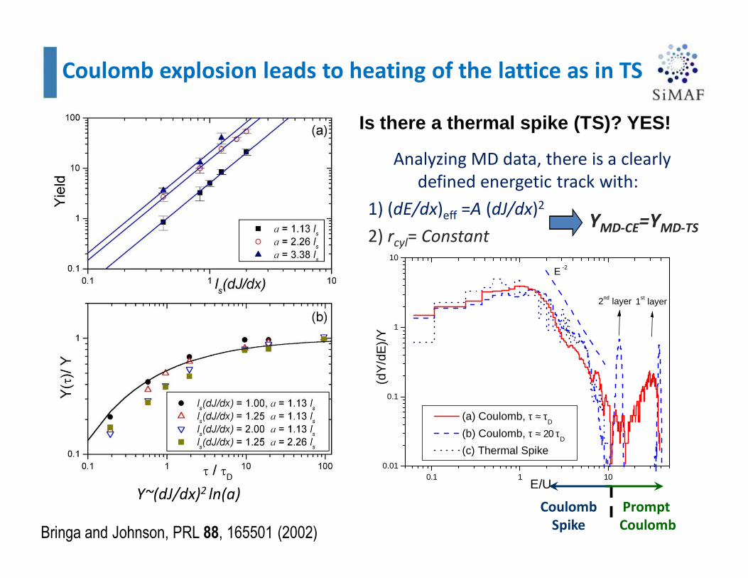
Coulomb explosion leads to heating of the lattice as in TS
Y~(dJ/dx)2 ln(a)
Is there a thermal spike (TS)? YES!
Analyzing MD data, there is a clearly
defined energetic track with:
1) (dE/dx)eff =A (dJ/dx)2
2) rcyl= ConstantY
MD-CE=Y
MD-TS
Coulomb
Spike
Prompt
CoulombBringa and Johnson, PRL 88, 165501 (2002)
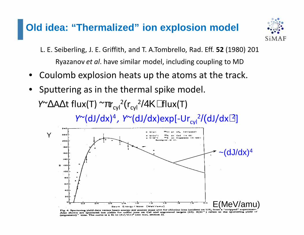
Old idea: “Thermalized” ion explosion model
L. E. Seiberling, J. E. Griffith, and T. A.Tombrello, Rad. Eff. 52 (1980) 201
Ryazanov et al. have similar model, including coupling to MD
• Coulomb explosion heats up the atoms at the track.
• Sputtering as in the thermal spike model.
Y~∆A∆t flux(T) ~πrcyl2(rcyl
2/4Κ) flux(T)
Y~(dJ/dx)4 , Y~(dJ/dx)exp[-Urcyl2/(dJ/dx)2]
Y
E(MeV/amu)
~(dJ/dx)4
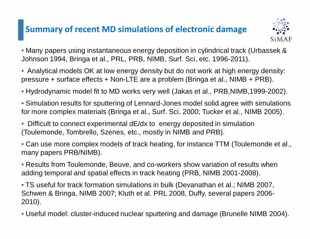
Summary of recent MD simulations of electronic damage
• Many papers using instantaneous energy deposition in cylindrical track (Urbassek & Johnson 1994, Bringa et al., PRL, PRB, NIMB, Surf. Sci, etc. 1996-2011).
• Analytical models OK at low energy density but do not work at high energy density: pressure + surface effects + Non-LTE are a problem (Bringa et al., NIMB + PRB).
• Hydrodynamic model fit to MD works very well (Jakas et al., PRB,NIMB,1999-2002).
• Simulation results for sputtering of Lennard-Jones model solid agree with simulations for more complex materials (Bringa et al., Surf. Sci. 2000; Tucker et al., NIMB 2005).
• Difficult to connect experimental dE/dx to energy deposited in simulation (Toulemonde, Tombrello, Szenes, etc., mostly in NIMB and PRB).
• Can use more complex models of track heating, for instance TTM (Toulemonde et al., many papers PRB/NIMB).
• Results from Toulemonde, Beuve, and co-workers show variation of results when adding temporal and spatial effects in track heating (PRB, NIMB 2001-2008).
• TS useful for track formation simulations in bulk (Devanathan et al.; NIMB 2007, Schwen & Bringa, NIMB 2007; Kluth et al. PRL 2008, Duffy, several papers 2006-2010).
• Useful model: cluster-induced nuclear sputtering and damage (Brunelle NIMB 2004).

Given all the approximations and limitations
involved …
Can we hope for quantitative agreement between MD
and experiments when electronic effects are important?
OR …
Is MD just pretty movies and pictures?
Two questions …
• Background and Introduction
– Track models
• Molecular Dynamics (MD) of damage in the electronic regime
– Thermal Spikes, Two Temperature Models and Coulomb Explosions.
• Examples
– Electronic sputtering, track formation: defects, phase change,
craters & bumps
• Conclusions and future outlook
OUTLINE
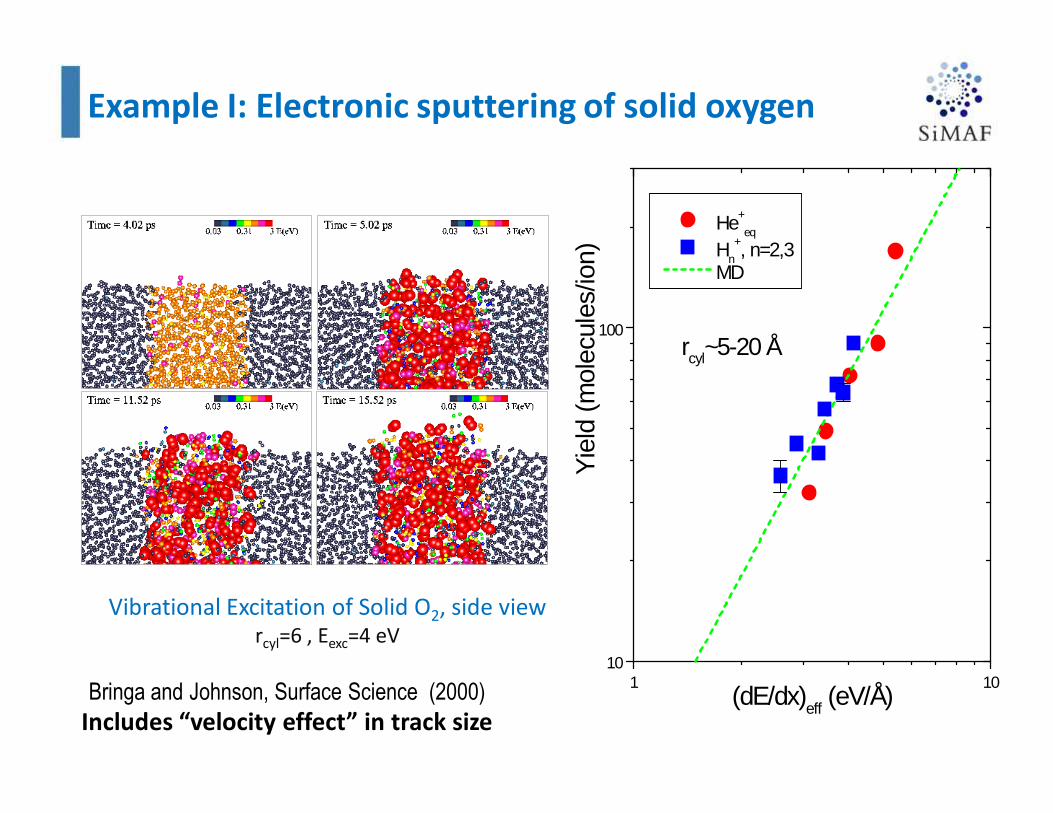
Vibrational Excitation of Solid O2, side viewrcyl=6 , Eexc=4 eV
1 1010
100rcyl~5-20 Å
He+
eq
Hn
+, n=2,3 MD
Yie
ld (
mol
ecul
es/io
n)
(dE/dx)eff (eV/Å)Bringa and Johnson, Surface Science (2000)
Includes “velocity effect” in track size
Example I: Electronic sputtering of solid oxygen
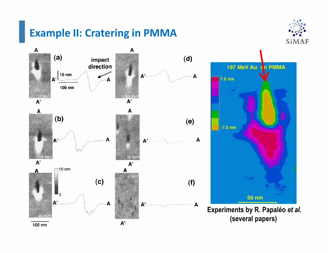
Experiments by R. Papaléo et al.
(several papers)
Example II: Cratering in PMMA
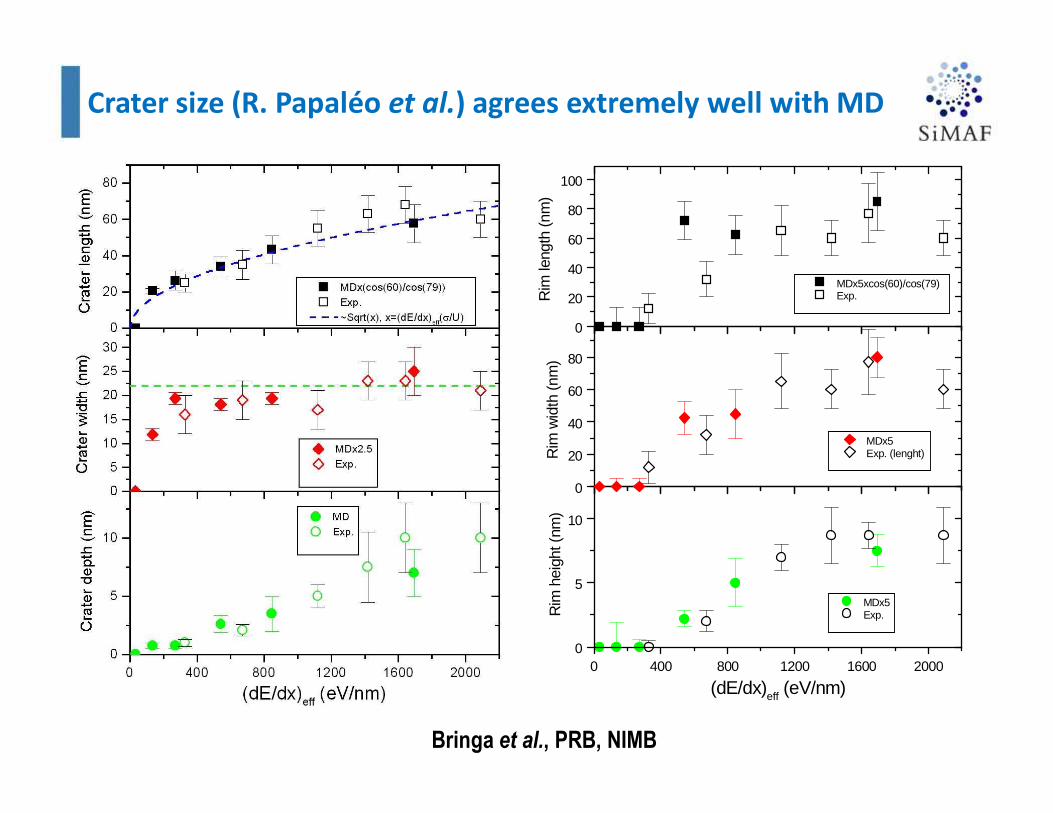
0 400 800 1200 1600 20000
5
10
MDx5 Exp.R
im h
eigh
t (nm
)
(dE/dx)eff (eV/nm)
0
20
40
60
80
MDx5 Exp. (lenght)R
im w
idth
(nm
)
0
20
40
60
80
100
MDx5xcos(60)/cos(79) Exp.R
im le
ngth
(nm
)
Bringa et al., PRB, NIMB
Crater size (R. Papaléo et al.) agrees extremely well with MD
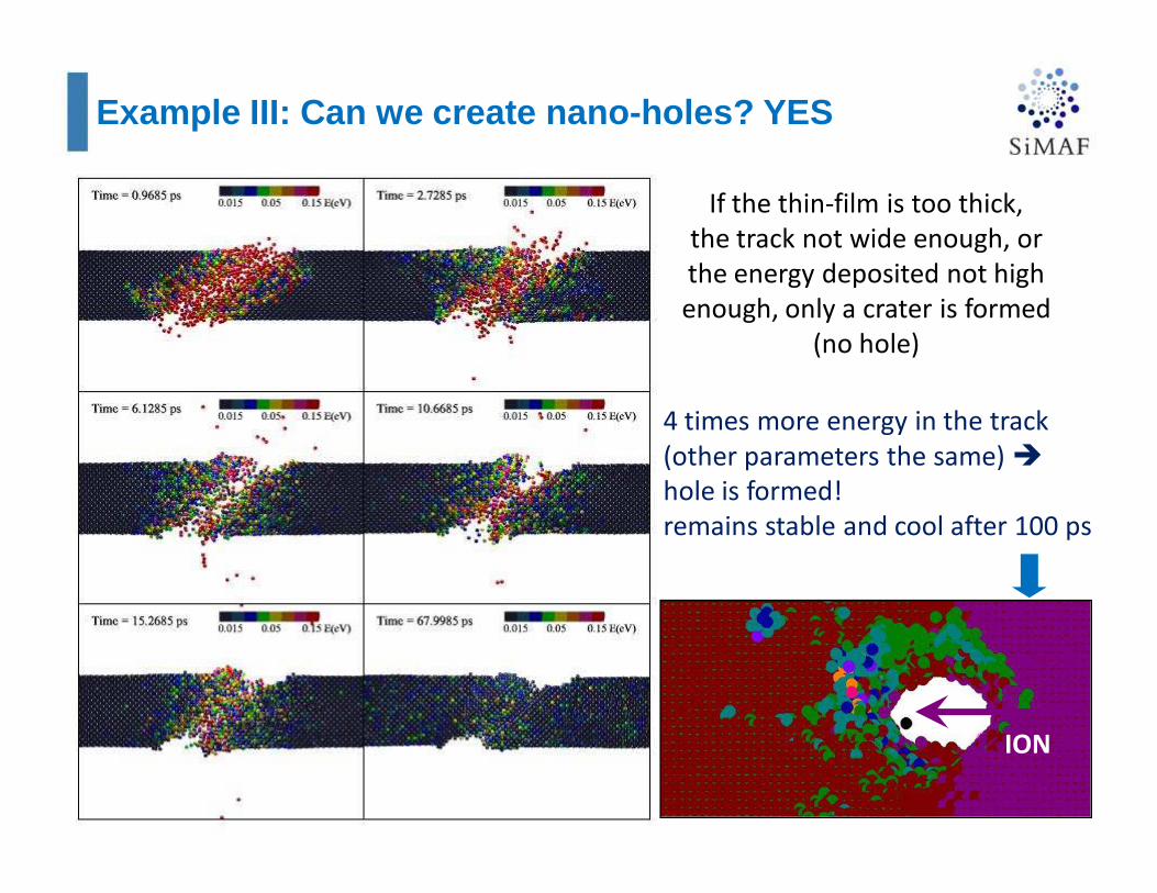
Example III: Can we create nano-holes? YES
If the thin-film is too thick,
the track not wide enough, or
the energy deposited not high
enough, only a crater is formed
(no hole)
4 times more energy in the track
(other parameters the same) �
hole is formed!
remains stable and cool after 100 ps
ION
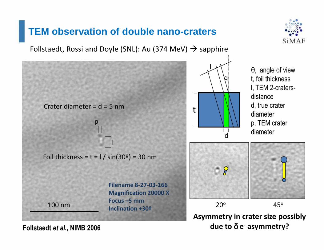
TEM observation of double nano-craters
Follstaedt, Rossi and Doyle (SNL): Au (374 MeV) � sapphire
θ, angle of viewt, foil thickness
l, TEM 2-craters-
distance
d, true crater
diameter
p, TEM crater
diameter
q
l
t
dl
Foil thickness = t = l / sin(30º) = 30 nm
p
Crater diameter = d = 5 nm
Filename 8-27-03-166
Magnification 20000 X
Focus –5 mm
Inclination +30º100 nm 20o 45o
Asymmetry in crater size possibly
due to δδδδ e- asymmetry?Follstaedt et al., NIMB 2006
Example IV: Tracks in ta-C create conducting nano-w ires
Schwen & Bringa, NIMB 2007
Simulations
and
experiments
display creation
of sp2 rich
region
Cosmic ray destroying a
carbon grain

Hillock formation (2 106 atoms, modified Brenner potential)
Schwen & Bringa, submitted (2011)
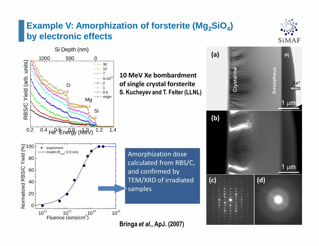
Example V: Amorphization of forsterite (Mg 2SiO4) by electronic effects
Bringa et al., ApJ. (2007)
10 MeV Xe bombardment
of single crystal forsterite
S. Kucheyev and T. Felter (LLNL)
Amorphization dose
calculated from RBS/C,
and confirmed by
TEM/XRD of irradiated
samples
0.2 0.4 0.6 0.8 1.0 1.2 1.4
1000 500 0
↓
↓
He+ Energy (MeV)
RB
S/C
Yie
ld (
arb.
uni
ts)
Si Depth (nm)
30 10 7 5×10¹²
2 1 0.5 virgin
Si
Mg
O↓
1011 1012 1013 1014
0
20
40
60
80
100 experiment model (R
track=2.8 nm)
Nor
mal
ized
RB
S/C
Yie
ld (
%)
Fluence (ions/cm2)
(a)
(b)
(c) (d)
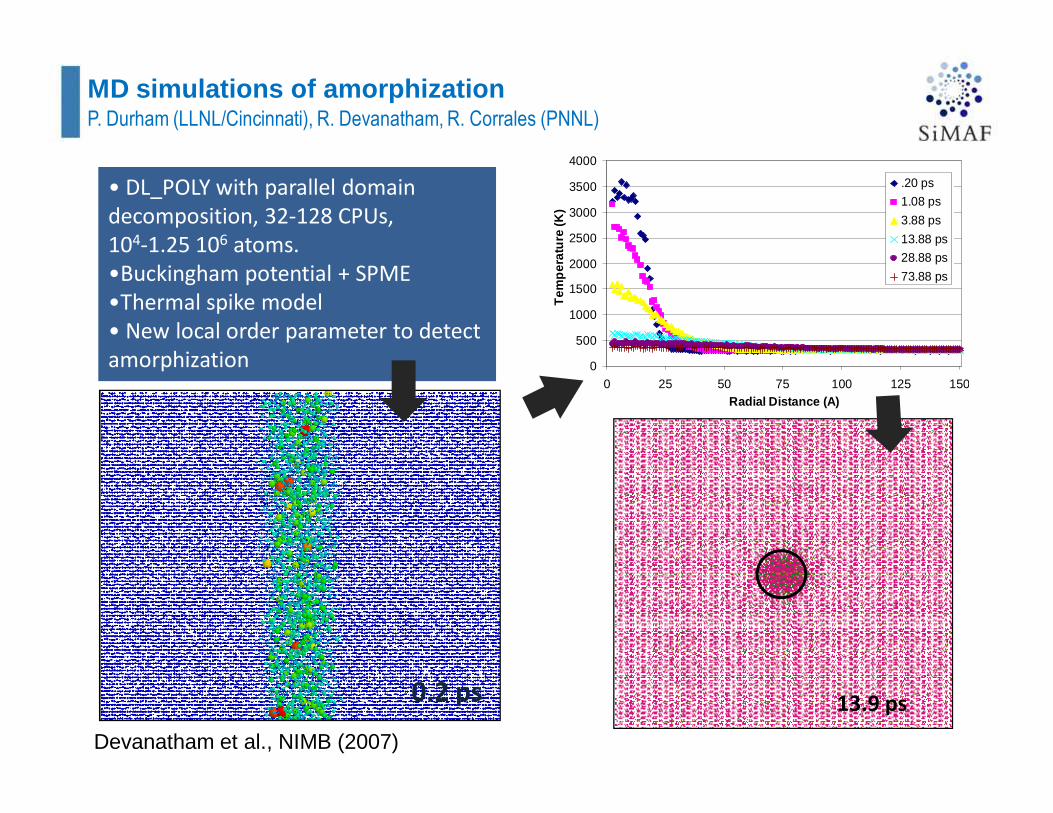
MD simulations of amorphization
0
500
1000
1500
2000
2500
3000
3500
4000
0 25 50 75 100 125 150Radial Distance (A)
Tem
pera
ture
(K)
.20 ps
1.08 ps
3.88 ps
13.88 ps
28.88 ps
73.88 ps
P. Durham (LLNL/Cincinnati), R. Devanatham, R. Corrales (PNNL)
• DL_POLY with parallel domain
decomposition, 32-128 CPUs,
104-1.25 106 atoms.
•Buckingham potential + SPME
•Thermal spike model
• New local order parameter to detect
amorphization
0.2 ps 13.9 ps
Devanatham et al., NIMB (2007)
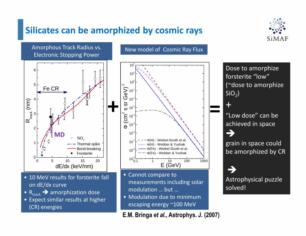
Amorphous Track Radius vs.
Electronic Stopping Power
• 10 MeV results for forsterite fall
on dE/dx curve
• Rtrack � amorphization dose
• Expect similar results at higher
(CR) energies
New model of Cosmic Ray Flux
Dose to amorphize
forsterite “low”
(~dose to amorphize
SiO2)
+“Low dose” can be
achieved in space
�
grain in space could
be amorphized by CR
�Astrophysical puzzle
solved!
0 5 10 15 200
1
2
3
4
5
6
SiO2
Thermal spike Bond-breaking Forsterite
Rtr
ack (
nm)
dE/dx (keV/nm)
Fe CR
0.1 1 10 100 100010-9
10-8
10-7
10-6
10-5
10-4
10-3
10-2
10-1
100
101
102
Φ (
cm2 s
sr
GeV
)-1
E (GeV)
Φ(H) - Wiebel-Sooth et al. Φ(H) - Webber & Yushak Φ(Fe) - Wiebel-Sooth et al. Φ(Fe) - Webber & Yushak
+ =
• Cannot compare to
measurements including solar
modulation … but …
• Modulation due to minimum
escaping energy ~100 MeV
E.M. Bringa et al., Astrophys. J. (2007)
Silicates can be amorphized by cosmic rays
MD
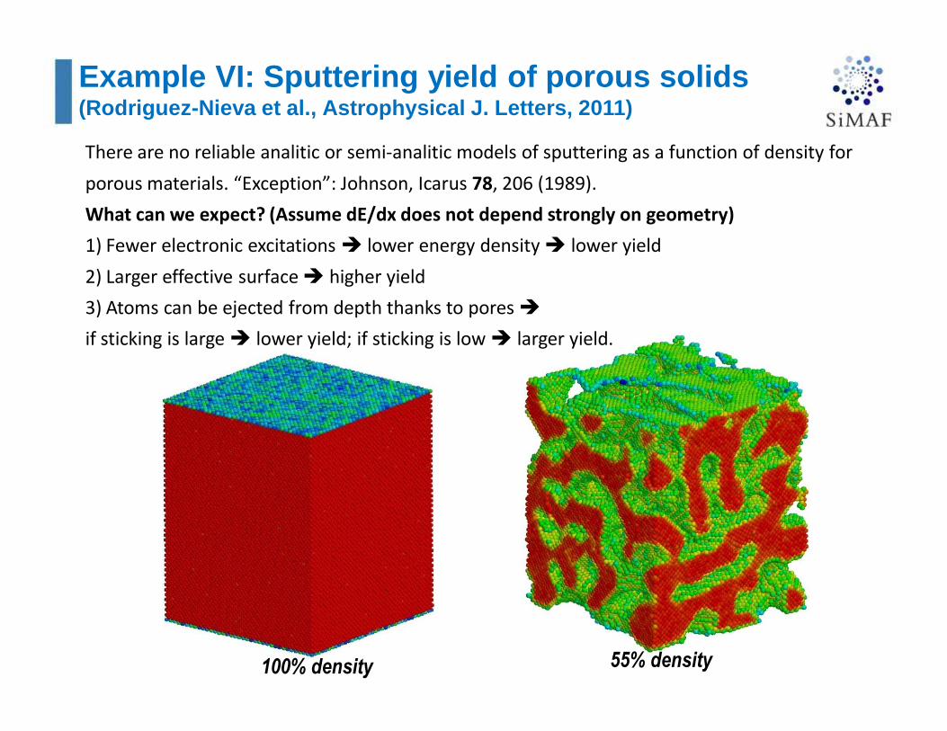
100% density 55% density
Example VI: Sputtering yield of porous solids(Rodriguez-Nieva et al., Astrophysical J. Letters, 2011)
There are no reliable analitic or semi-analitic models of sputtering as a function of density for
porous materials. “Exception”: Johnson, Icarus 78, 206 (1989).
What can we expect? (Assume dE/dx does not depend strongly on geometry)
1) Fewer electronic excitations � lower energy density � lower yield
2) Larger effective surface � higher yield
3) Atoms can be ejected from depth thanks to pores �
if sticking is large � lower yield; if sticking is low � larger yield.
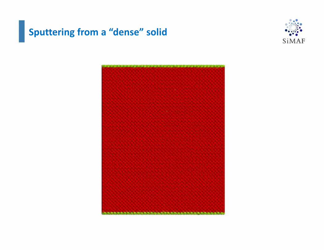
Sputtering from a “dense” solid
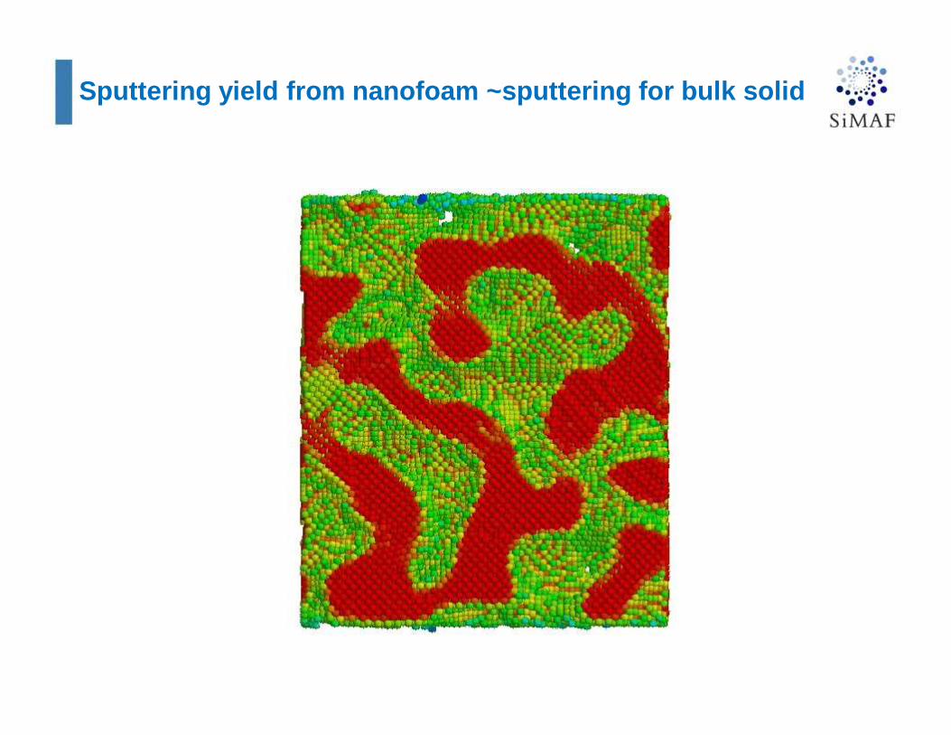
Sputtering yield from nanofoam ~sputtering for bulk solid
• Simple models can account for many experimental res ults!
• But cannot account for many other experimental results ….
• Poor understanding of: synergy between nuclear and electronic dE/dx + nuclear
reactions, dE/dx at surfaces or nanostructures (islands, foams, nanoprecipitates,
interfaces, etc.), charge-state effects (in dE/dx, ion ejection, charge exchange
for both target & projectile, etc.), dE/dx for cluster projectiles, statistics of dE/dx
and track size, etc.
• Beware of limitations due to system size and total simulated time!
• Empirical potentials offer severe constrains and have to be used with care:
- where they were not intended to be used (phase transitions; high P/T;
core-shell potentials for oxides problematic in radiation simulations).
- where classical MD does not work properly (high P/T).
CONCLUSIONS
• Multi-scale models needed for improved simulations:
-coupling to FEM for larger system size;
-more general accelerated dynamics or KMC for defect evolution;
-coupling to MC/DFT/TB/TDDFT/naTB for better excitation treatment
-empirical potentials which depend dynamically on electronic state (high P/T,
excitations, electron density – Khakshouri et al., PRB 2008-), etc.
• Better ion-electron models are already available and are discussed by
several presentations in this workshop (Artacho, Caro, Correa, Fisher,
Foulkes, Lu). The electron Force Field potential (eFF, Su & Goddard, PRL
2007) is another option for light elements.
• Still lacking reliable and efficient models for swift heavy ions .
FUTURE- I
• More CPU/GPU processing for MD parameter sweeping will
speed up research, allowing for improved models, better
potentials, and increasing statistics and parameter sweeping.
LAMMPS/DL_POLY, etc. already have GPU versions.
• Need more links to experiments: measurement of surface and
bulk defects (AFM/STM/TEM simulation –Victoria’s talk-), IR
spectra (Caturla et al.), X-ray diffraction simulation, mechanical
properties, etc.
• Similarities with electronic excitations by photons (UV, lasers)
should be exploited.
• Need more experiments!
FUTURE- II