Embed Size (px)
Citation preview

Radiation hardness evaluations of 65nm fully depleted silicon on insulator and bulk processes
by measuring single event transient pulse widths and single event upset rates
Jun Furuta*, Eiji Sonezaki, and Kazutoshi Kobayashi
Department of Electronics, Graduate School of Science and Technology, Kyoto Institute of Technology, Kyoto 606-8585, JapanE-mail: [email protected]
Received September 11, 2014; revised December 9, 2014; accepted December 24, 2014; published online March 19, 2015
We measure single event transient (SET) pulse widths on inverter chains and single event upset (SEU) rates on flip-flops (FFs) fabricated in 65nmfully depleted silicon on insulator (FD-SOI) and bulk processes. The layout designs of test chips are strictly identical between their processesbesides buried oxide (BOX) layers. Experimental results show that neutron-induced SEU and SET rates in the FD-SOI process are 230' and 450'lower than those in the bulk process, respectively. © 2015 The Japan Society of Applied Physics
1. Introduction
According to process scaling down to nanometers, LSI ismore sensitive to radiation effects in space and terrestrialenvironments. At ground level, single event effects (SEEs)are significant issues for LSI reliability, which is caused by αparticles and neutrons. When a charged particle is incidenton the LSI, its ionizing effect generates electron–hole pairsin p- and n-wells. Generated charge is collected into atransistor’s drain region and its output is temporally flipped,which is called a soft error. If a charged particle is incident ona combinational circuit, it induces a transient pulse, which isnamed a single event transient (SET). In contrast, if a chargedparticle is incident on a storage cell such as static randomaccess memories (SRAMs) and flip-flops (FFs), its storedvalue is flipped. It is called a single event upset (SEU). Softerror rates (SERs) per chip increase according to the processscaling since transistor density exponentially increasesyearly.1) Therefore, a radiation-hardened design is requiredto achieve high reliability in advanced technologies.
The triple modular redundancy (TMR) FF is thefundamental circuit design for the reliability, which consistsof three identical FFs and a majority-voting circuit.2) Theoutput of the TMR FF is determined by majority voting ofthree FFs and it remains correct even if a particle is incidenton one FF and flips its stored value. The TMR FF has strongradiation resilience while it occupies a huge area andconsumes much power. However, the soft error resilienceon radiation-hardened FFs is markedly reduced in the 90 nmprocess and beyond. Jagannathan et al. reported neutron-and α-particle-induced SERs on 40 nm TMR FF and severalredundant FFs.3) TMR FF has only 3.3× higher soft errorresilience than non redundant FF owing to multi-node chargecollection.4) A radiation strike can flip several nodes, andthese flips are simultaneous flips of stored values.
Fully depleted silicon on insulator (FD-SOI) transistorsare one of the most effective solutions for the single eventeffect.5–7) In an SOI process, transistors are separated into thep- and n-well by buried oxide (BOX) layers. Almost all of thegenerated charge cannot be collected into a drain region,when a particle is incident on a chip and generates electron–hole pairs in the p- and n-wells. Therefore, SOI transistorshave higher soft error resilience than bulk transistors withoutarea, delay, and power penalties.
In this work, we measure neutron-induced SEU and SETin a 65 nm FD-SOI technology and a 65 nm bulk technol-
ogy.8) The layout designs of test chips are strictly identicalbetween FD-SOI and bulk processes except for thin BOXlayers. Test chips consist of a shift-register-based flip-floparray and 6 types of inverter chain with a time-to-digitalconverter in order to measure SEU rates on FFs and SETpulse widths.
The paper is organized as follows. In Sect. 2, we explainsoft error mechanisms in bulk and FD-SOI processes. InSect. 3, we explain the test circuit structure. In Sect. 4, wediscuss the experimental results. In Sect. 5, we conclude thispaper.
2. Soft error mechanism
At ground level, soft errors are caused by α particles emittedfrom package material and neutrons generated in theatmosphere by cosmic rays.9) When an α particle is incidenton a bulk transistor, electron–hole pairs are generated by itsionizing effect along the particle track, as shown in Fig. 1(a).Generated electrons in the p-well are collected into thedrain region of the nMOS transistor by funneling, drift, anddiffusion.10) The drain output can be flipped by collectedelectrons transiently. Its radiation effect is termed a SEE. Incontrast, neutrons do not generate electron–hole pairs directly.Their effects occur through nuclear collisions with Si atoms,which generate secondary particles. Then, they generateelectron–hole pairs. When electron–hole pairs are generatedin a combinational circuit, they induce a transient voltagepulse on any node in a circuit, which is called a SET. Whenelectron–hole pairs are generated in a sequential element, theymay flip the stored value, which is called a SEU.
n+ n+
p-well
Chargedparticle
(a)
n+ n+
p-well
SiO2
Chargedparticle
BO
X la
yer
Bod
y la
yer
(b)
Fig. 1. (Color online) Single event effect on a bulk transistor and on aSOI transistor: (a) bulk process and (b) SOI process.
Japanese Journal of Applied Physics 54, 04DC15 (2015)
http://dx.doi.org/10.7567/JJAP.54.04DC15
REGULAR PAPER
04DC15-1 © 2015 The Japan Society of Applied Physics

In an FD-SOI process, transistors are separated from p- andn-wells by BOX layers as shown in Fig. 1(b). Radiation-induced carriers in well regions are not collected into drainregions, and carriers in a body are only collected. In a bulkprocess, the charge-collection range by funneling is severalhundred nanometers, which is used in the depth of sensitivevolume for soft error simulation.11,12) In contrast, the bodythickness in fabricated FD-SOI process is 12 nm. Therefore,the amount of collected charge is much smaller in theFD-SOI transistor than in the bulk transistor and FD-SOItransistor achieves a high soft error resilience.6,13–15)
3. Test circuit structure
To measure the SET pulse width on inverters and SEU onFFs, we implement two test circuits. In this section, weexplain them in detail.
3.1 SET pulse width measurement circuitInverter chains and time-to-digital converters (TDCs) areembedded to measure SET pulse width distributions.Figure 2 shows the schematic circuit diagram of embeddedinverter chains and a TDC. It is connected to a 16-inverterchain through the logic tree of NAND and NOR gates.Each inverter chain consists of 50 inverters. This structuresuppresses the propagation-induced effect and measures SETpulse widths accurately.16,17) The propagation-induced effectimplies that injected SET pulses are broadening or shrinkinglinearly while SET pulses propagate through a logic chain.It is explained by the hysteretic modulation in the thresholdvoltage by the floating body effect and negative biastemperature instability (NBTI).18) Some researchers reportthat the pulse modulation amount is less than 2 ps perinverter.18–21) We assume that the modulation amount is lessthan 100 ps even if the SET pulse is injected in the firstinverter of the implemented inverter chain.
Figure 3 shows a circuit structure for measuring SET pulsewidths. The implemented TDC is based on a ring oscillatorand a counter.22) The SET pulse width is roughly measuredby a counter circuit and precisely measured by D-latches.If an SET is injected from the target, the NAND gate isactivated and the ring oscillator remains oscillating while theSET pulse is injected, as shown in Fig. 4. The counter detectsfall transitions of the ring oscillator and counts its frequency,while the latches hold each output value of the logic gates inthe oscillator immediately when the ring oscillator stops. The
SET pulse width can be computed on the basis of the numberof oscillations stored in the counter and the states of thelatches. Therefore, it can measure SET pulse widths by theresolution of the delay time of the inverter in the ringoscillator. When two SET pulses are injected in the inverterchain, the counter counts the sum of their widths. One FF anda NAND gate are inserted to detect an SET occurrence andblock another SET pulse from the inverter chain. The signalscalled “set” are external inputs, which are used to initializestored values of the counter, the D-latches, and the FF.
We implement 7-stage ring oscillators and dividers togenerate rectangular pulses. We measure their pulse widthsusing the TDCs fabricated in 65 nm FD-SOI and bulkprocesses in order to obtain the resolution of TDCs. Figure 5shows the calibration results. The resolutions of the TDCs are19.6 and 37.1 ps, respectively, when the supply voltage is1.2V. The FD-SOI transistors have a lower threshold voltageand higher a on-state current than the bulk transistor. TheFD-SOI transistors also have a smaller junction capacitance
50 inverters16
inve
rter
cha
ins
NOR NAND...
time-to-digital converterIN
Fig. 2. Schematic circuit diagram of embedded inverter chain and time-to-digital converter.
8-bit COUNTER
latch2 latch6 latch7set
FFVSS
set
INOUT
7-stage ring oscillator
latch1
set
set
set
set
IN
CLK CLK CLK CLK
SET detector
N1 N7N0
Fig. 3. Time-to-digital converter to measure SET pulse width.
SET pulse widthN0
cou
nter
1 2 3
N7
N1
Oscillation
latc
h1
data hold
Fig. 4. (Color online) Operating example of time-to-digital converter.
0
40
80
120
0 500 1000 1500 2000 2500 3000
Input Pulse Width [ps]
Out
put o
f TD
C
f(x) = x37.1 ps
- 0.01
FD-SOIbulk
f(x) = x19.6 ps
- 3.7
Fig. 5. (Color online) Calibration results of TDC fabricated in 65 nmFD-SOI and bulk processes.
Jpn. J. Appl. Phys. 54, 04DC15 (2015) J. Furuta et al.
04DC15-2 © 2015 The Japan Society of Applied Physics

between the diffusion region and the well region since thethin BOX layer is inserted between them, and the BOX layeris thicker than the depletion region of the bulk transistor.Thus, the resolution is better in the FD-SOI process than inthe bulk process. In the circuit-level simulation, delay timesof an inverter with fanout 1 are 21.1 ps in the 65 nm bulkprocess and 13.3 ps in the 65 nm FD-SOI process.
3.2 FF array for measuring SEU ratesTo measure SEU rates on FFs, we prepare an FF array on thebasis of a shift register, which is constructed using FFs and aclock buffer chain.23,24) Figure 6 shows the schematic of theFF array and Fig. 7 shows that of the implemented FF. It hasno clock tree to simplify the layout structure, and clock bufferchains are used to apply a clock signal. Well contacts areinserted every 10 FFs to stabilize the well potential in theimplemented FF array. In accelerated tests, the FF array isinitialized using an arbitrary pattern. During irradiation, itsclock signal is fixed at “0” or “1” in order to maintain thestored value. All stored values are retrieved after irradiationand compared with the initial pattern. The soft error ratecan be calculated from the number of flipped stored values,neutron flux, and the number of implemented FFs.
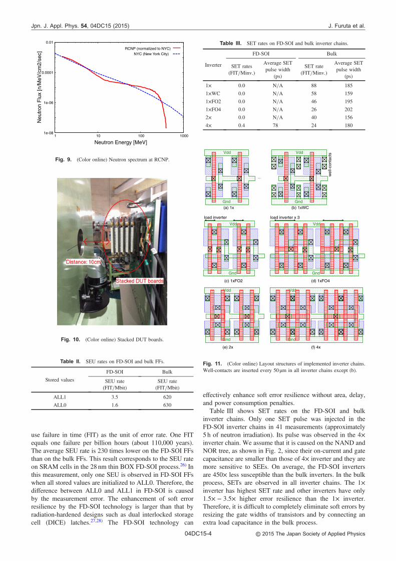
3.3 Test chip structureFigure 8 shows the fabricated test chip micrograph with afloor plan and a layout pattern. Test chips were fabricated inthe bulk process and the thin BOX FD-SOI process namedSOTB. In the SOTB process, the thicknesses of the BOXlayer and body layer are 10 and 12 nm, respectively. Thelayout designs of the test chips are strictly identical betweenSOTB and bulk processes in order to compare soft error rates.
However, the channel impurity concentrations and thethreshold voltage of the SOTB transistors are lower thanthose of the bulk transistors.25) The test chip includes 829units of SET pulse measurement circuits and a 140,000 bit FFarray. To measure the dependences of SETs, we implemented6 different types of inverter chain. The parameters of theimplemented inverter chains are summarized in Table I, andFig. 11 shows their layout structures.
4. Experimental results
4.1 Experimental setupAccelerated tests were performed by the spallation neutronbeam at the research center for nuclear physics (RCNP),Osaka University. Figure 9 shows the neutron beamspectrum in comparison with the terrestrial neutron spectrumat the ground level of New York. The average acceleratedfactor is 2.9 × 10⁸. We measured 12 FD-SOI test chips and12 bulk test chips simultaneously using stacked DUT boards,as shown in Fig. 10. Their supply voltages were fixed at1.2V. All stored values of the FF array are initialized to “0”or “1”. Therefore, the SET pulses on clock buffer chains arenegligible since they cannot flip the stored values on FFs.During irradiation, the clock signal is fixed at “1” or “0” tokeep the master latches or slave latches in FFs in the holdstate. The stored values on the FF array and TDCs areretrieved and initialized every 7min.
4.2 Comparison of SEU rates and SET rates between theFD-SOI and the bulk processesTable II shows SEU rates on the FD-SOI and bulk FFs. We
10 FFs
FF FF FF FF FF FFtap FF
FF FF FF FF FF FF
tap FF
FF FF FF FF FF FFtap FF
FF FF FF FF FF
FF FF FF FF FF
FF FF FF FF FF
FF FF FF FF FF FF
tap FF FF FF FF FF FF
FF FF FF
IN
FF FFOUT
CLK
VDD
VDD
GND
GND
GND taptap
taptap
Fig. 6. (Color online) Schematic structure of the FF array.
CLK
CLKCLK
CLK
CLK
CLKCLK
CLKIN OUT
1x1x
2.5x 6x4x 5x
CLKin
Master Latch Slave Latch
CLKCLK
Fig. 7. Schematic structure of the implemented FF.
6.2 mm
200,000 bit Flip-Flip Array
1x inverter chain TDC
829 Units of SET Meas. Circuit
Fig. 8. (Color online) Fabricated test chip micrograph with floor plan andlayout pattern.
Table I. The parameters of implemented inverter chains.
Inverterchain
Drivestrength
FanoutWell-contact
interval(µm)
Drain area(arb. unit)
1× 1 1 50 1
1×WC 1 1 2 1
1×FO2 1 2 50 1
1×FO4 1 4 50 1
2× 2 1 50 1
4× 4 1 50 2
Jpn. J. Appl. Phys. 54, 04DC15 (2015) J. Furuta et al.
04DC15-3 © 2015 The Japan Society of Applied Physics
use failure in time (FIT) as the unit of error rate. One FITequals one failure per billion hours (about 110,000 years).The average SEU rate is 230 times lower on the FD-SOI FFsthan on the bulk FFs. This result corresponds to the SEU rateon SRAM cells in the 28 nm thin BOX FD-SOI process.26) Inthis measurement, only one SEU is observed in FD-SOI FFswhen all stored values are initialized to ALL0. Therefore, thedifference between ALL0 and ALL1 in FD-SOI is causedby the measurement error. The enhancement of soft errorresilience by the FD-SOI technology is larger than that byradiation-hardened designs such as dual interlocked storagecell (DICE) latches.27,28) The FD-SOI technology can
effectively enhance soft error resilience without area, delay,and power consumption penalties.
Table III shows SET rates on the FD-SOI and bulkinverter chains. Only one SET pulse was injected in theFD-SOI inverter chains in 41 measurements (approximately5 h of neutron irradiation). Its pulse was observed in the 4×inverter chain. We assume that it is caused on the NAND andNOR tree, as shown in Fig. 2, since their on-current and gatecapacitance are smaller than those of 4× inverter and they aremore sensitive to SEEs. On average, the FD-SOI invertersare 450× less susceptible than the bulk inverters. In the bulkprocess, SETs are observed in all inverter chains. The 1×inverter has highest SET rate and other inverters have only1.5× − 3.5× higher error resilience than the 1× inverter.Therefore, it is difficult to completely eliminate soft errors byresizing the gate widths of transistors and by connecting anextra load capacitance in the bulk process.
Table II. SEU rates on FD-SOI and bulk FFs.
Stored values
FD-SOI Bulk
SEU rate(FIT=Mbit)
SEU rate(FIT=Mbit)
ALL1 3.5 620
ALL0 1.6 630
1e-08
1e-06
0.0001
0.01
1 10 100 1000
Neu
tron
Flu
x [n
/MeV
/cm
2/se
c]
Neutron Energy [MeV]
RCNP (normalized to NYC)NYC (New York City)
Fig. 9. (Color online) Neutron spectrum at RCNP.
Fig. 10. (Color online) Stacked DUT boards.
Table III. SET rates on FD-SOI and bulk inverter chains.
Inverter
FD-SOI Bulk
SET rates(FIT=Minv.)
Average SETpulse width
(ps)
SET rate(FIT=Minv.)
Average SETpulse width
(ps)
1× 0.0 N=A 88 185
1×WC 0.0 N=A 58 159
1×FO2 0.0 N=A 46 195
1×FO4 0.0 N=A 26 202
2× 0.0 N=A 40 156
4× 0.4 78 24 180
(a) 1x (b) 1xWC
Vdd
Gnd
Vdd
Gnd
wel
l-con
tact
s
(c) 1xFO2
Vdd
Gnd
(d) 1xFO4
Vdd
Gnd
load inverter load inverter x 3
Vdd
Gnd
(e) 2x
Vdd
Gnd
(f) 4x
Fig. 11. (Color online) Layout structures of implemented inverter chains.Well-contacts are inserted every 50 µm in all inverter chains except (b).
Jpn. J. Appl. Phys. 54, 04DC15 (2015) J. Furuta et al.
04DC15-4 © 2015 The Japan Society of Applied Physics
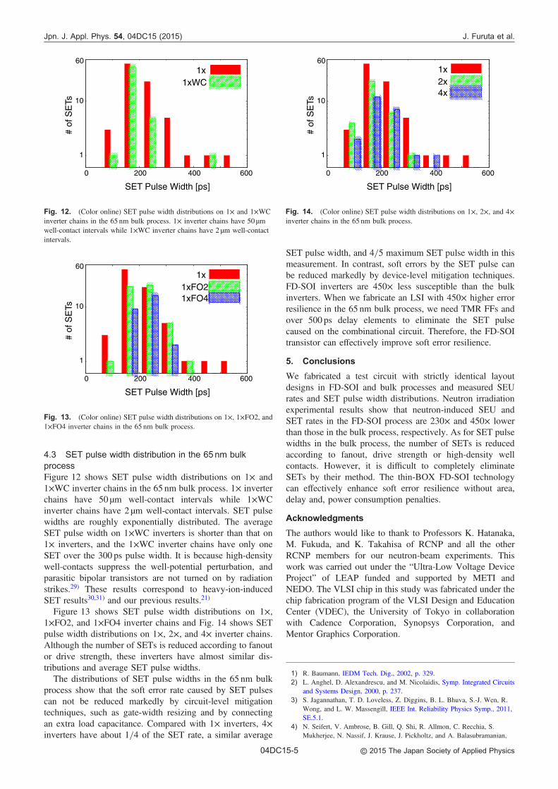
4.3 SET pulse width distribution in the 65nm bulkprocessFigure 12 shows SET pulse width distributions on 1× and1×WC inverter chains in the 65 nm bulk process. 1× inverterchains have 50 µm well-contact intervals while 1×WCinverter chains have 2 µm well-contact intervals. SET pulsewidths are roughly exponentially distributed. The averageSET pulse width on 1×WC inverters is shorter than that on1× inverters, and the 1×WC inverter chains have only oneSET over the 300 ps pulse width. It is because high-densitywell-contacts suppress the well-potential perturbation, andparasitic bipolar transistors are not turned on by radiationstrikes.29) These results correspond to heavy-ion-inducedSET results30,31) and our previous results.21)
Figure 13 shows SET pulse width distributions on 1×,1×FO2, and 1×FO4 inverter chains and Fig. 14 shows SETpulse width distributions on 1×, 2×, and 4× inverter chains.Although the number of SETs is reduced according to fanoutor drive strength, these inverters have almost similar dis-tributions and average SET pulse widths.
The distributions of SET pulse widths in the 65 nm bulkprocess show that the soft error rate caused by SET pulsescan not be reduced markedly by circuit-level mitigationtechniques, such as gate-width resizing and by connectingan extra load capacitance. Compared with 1× inverters, 4×inverters have about 1=4 of the SET rate, a similar average
SET pulse width, and 4=5 maximum SET pulse width in thismeasurement. In contrast, soft errors by the SET pulse canbe reduced markedly by device-level mitigation techniques.FD-SOI inverters are 450× less susceptible than the bulkinverters. When we fabricate an LSI with 450× higher errorresilience in the 65 nm bulk process, we need TMR FFs andover 500 ps delay elements to eliminate the SET pulsecaused on the combinational circuit. Therefore, the FD-SOItransistor can effectively improve soft error resilience.
5. Conclusions
We fabricated a test circuit with strictly identical layoutdesigns in FD-SOI and bulk processes and measured SEUrates and SET pulse width distributions. Neutron irradiationexperimental results show that neutron-induced SEU andSET rates in the FD-SOI process are 230× and 450× lowerthan those in the bulk process, respectively. As for SET pulsewidths in the bulk process, the number of SETs is reducedaccording to fanout, drive strength or high-density wellcontacts. However, it is difficult to completely eliminateSETs by their method. The thin-BOX FD-SOI technologycan effectively enhance soft error resilience without area,delay and, power consumption penalties.
Acknowledgments
The authors would like to thank to Professors K. Hatanaka,M. Fukuda, and K. Takahisa of RCNP and all the otherRCNP members for our neutron-beam experiments. Thiswork was carried out under the “Ultra-Low Voltage DeviceProject” of LEAP funded and supported by METI andNEDO. The VLSI chip in this study was fabricated under thechip fabrication program of the VLSI Design and EducationCenter (VDEC), the University of Tokyo in collaborationwith Cadence Corporation, Synopsys Corporation, andMentor Graphics Corporation.
1) R. Baumann, IEDM Tech. Dig., 2002, p. 329.2) L. Anghel, D. Alexandrescu, and M. Nicolaidis, Symp. Integrated Circuits
and Systems Design, 2000, p. 237.3) S. Jagannathan, T. D. Loveless, Z. Diggins, B. L. Bhuva, S.-J. Wen, R.
Wong, and L. W. Massengill, IEEE Int. Reliability Physics Symp., 2011,SE.5.1.
4) N. Seifert, V. Ambrose, B. Gill, Q. Shi, R. Allmon, C. Recchia, S.Mukherjee, N. Nassif, J. Krause, J. Pickholtz, and A. Balasubramanian,
1xWC1x
1
10
0 200 400 600
SET Pulse Width [ps]
# of
SE
Ts
60
Fig. 12. (Color online) SET pulse width distributions on 1× and 1×WCinverter chains in the 65 nm bulk process. 1× inverter chains have 50 µmwell-contact intervals while 1×WC inverter chains have 2 µm well-contactintervals.
1xFO21x
1xFO4
1
10
0 200 400 600
SET Pulse Width [ps]
# of
SE
Ts
60
Fig. 13. (Color online) SET pulse width distributions on 1×, 1×FO2, and1×FO4 inverter chains in the 65 nm bulk process.
2x1x
4x
1
10
0 200 400 600
SET Pulse Width [ps]
# of
SE
Ts
60
Fig. 14. (Color online) SET pulse width distributions on 1×, 2×, and 4×inverter chains in the 65 nm bulk process.
Jpn. J. Appl. Phys. 54, 04DC15 (2015) J. Furuta et al.
04DC15-5 © 2015 The Japan Society of Applied Physics

IEEE Int. Reliability Physics Symp., 2010, p. 188.5) G. Gasiot, P. Roche, and P. Flatresse, IEEE Int. Reliability Physics Symp.,
2008, p. 192.6) K. Hirose, H. Saito, Y. Kuroda, S. Ishii, Y. Fukuoka, and D. Takahashi,
IEEE Trans. Nucl. Sci. 49, 2965 (2002).7) Y. Yanagawa, K. Hirose, H. Saito, D. Kobayashi, S. Fukuda, S. Ishii, D.
Takahashi, K. Yamamoto, and Y. Kuroda, IEEE Trans. Nucl. Sci. 53, 3575(2006).
8) E. Sonezaki, J. Furuta, and K. Kobayashi, Ext. Abstr. Int. Conf. Solid StateDevices and Materials, 2014, p. 840.
9) T. Karnik and P. Hazucha, IEEE Trans. Dependable Secure Comput. 1, 128(2004).
10) J. C. Pickel, IEEE Trans. Nucl. Sci. 29, 2049 (1982).11) S. Yoshimoto, T. Amashita, M. Yoshimura, Y. Matsunaga, H. Yasuura, S.
Izumi, H. Kawaguchi, and M. Yoshimoto, IEEE Int. On-Line TestingSymp., 2012, p. 138.
12) S. Abe, Y. Watanabe, N. Shibano, N. Sano, H. Furuta, M. Tsutsui, T.Uemura, and T. Arakawa, IEEE Trans. Nucl. Sci. 59, 965 (2012).
13) V. Ferlet-Cavrois, G. Gasiot, C. Marcandella, C. D’Hose, O. Flament, O.Faynot, J. du Port de Pontcharra, and C. Raynaud, IEEE Trans. Nucl. Sci.49, 2948 (2002).
14) J. Baggio, V. Ferlet-Cavrois, D. Lambert, P. Paillet, F. Wrobel, K. Hirose,H. Saito, and E. W. Blackmore, IEEE Trans. Nucl. Sci. 52, 2319 (2005).
15) D. R. Ball, M. L. Alles, R. D. Schrimpf, and S. Cristoloveanu, IEEE Int.SOI Conf., 2010, p. 1.
16) P. Chen, S.-I. Liu, and J. Wu, IEEE Trans. Circuits Syst. II 47, 954 (2000).17) B. Gill, N. Seifert, and V. Zia, IEEE Int. Reliability Physics Symp., 2009,
p. 199.18) R. Harada, Y. Mitsuyama, M. Hashimoto, and T. Onoye, IEEE Trans. Nucl.
Sci. 60, 2630 (2013).19) V. Ferlet-Cavrois, P. Paillet, D. McMorrow, N. Fel, J. Baggio, S. Girard, O.
Duhamel, J. S. Melinger, M. Gaillardin, J. R. Schwank, P. E. Dodd, M. R.Shaneyfelt, and J. A. Felix, IEEE Trans. Nucl. Sci. 54, 2338 (2007).
20) M. J. Gadlage, J. R. Ahlbin, B. Narasimham, V. Ramachandran, C. A.Dinkins, N. D. Pate, B. L. Bhuva, R. D. Schrimpf, L. W. Massengill, R. L.Shuler, and D. McMorrow, IEEE Trans. Device Mater. Reliab. 10, 157(2010).
21) J. Furuta, C. Hamanaka, K. Kobayashi, and H. Onodera, IEEE Int.Reliability Physics Symp., 2011, 5B.2.1.
22) J. Furuta, R. Yamamoto, K. Kobayashi, and H. Onodera, IEEE Int.Reliability Physics Symp., 2012, SE.5.1.
23) J. Furuta, C. Hamanaka, K. Kobayashi, and H. Onodera, Asia and SouthPacific Design Automation Conf., 2011, p. 83.
24) J. Furuta, K. Kobayashi, and H. Onodera, IEEE Int. Reliability PhysicsSymp., 2013, 6C.3.1.
25) N. Sugii, R. Tsuchiya, T. Ishigaki, Y. Morita, H. Yoshimoto, and S.Kimura, IEEE Trans. Electron Devices 57, 835 (2010).
26) P. Roche, J.-L. Autran, G. Gasiot, and D. Munteanu, IEDM Tech. Dig.,2013, 31.1.1.
27) P. Hazucha, T. Karnik, S. Walstra, B. Bloechel, J. Tschanz, J. Maiz, K.Soumyanath, G. Dermer, S. Narendra, V. De, and S. Borkar, Proc. IEEECustom Integrated Circuits Conf., 2003, p. 617.
28) D. Krueger, E. Francom, and J. Langsdorf, IEEE Int. Solid-State CircuitsConf., 2008, p. 94.
29) T. Nakauchi, N. Mikami, A. Oyama, H. Kobayashi, H. Usui, and J. Kase,IEEE Int. Reliability Physics Symp., 2008, p. 187.
30) B. Narasimham, B. L. Bhuva, R. D. Schrimpf, L. W. Massengill, M. J.Gadlage, W. T. Holman, A. F. Witulski, W. H. Robinson, J. D. Black, J. M.Benedetto, and P. H. Eaton, European Conf. Radiation and Its Effects onComponents and Systems, 2007, p. 1.
31) O. A. Amusan, L. W. Massengill, B. L. Bhuva, S. Das Gupta, A. F.Witulski, and J. R. Ahlbin, IEEE Trans. Nucl. Sci. 54, 2060 (2007).
Jpn. J. Appl. Phys. 54, 04DC15 (2015) J. Furuta et al.
04DC15-6 © 2015 The Japan Society of Applied Physics