Embed Size (px)
Citation preview

Digital IC Introduction EE141
1
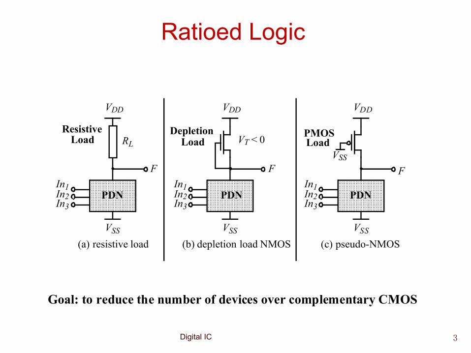
Ratioed Logic

Digital IC 2
Ratioed Logic design • Basic concept • Resistive load • Depletion NMOS • Pseudo NMOS • DCVSL logic • Pseudo NMOS logic effort
Digital IC 3
Ratioed Logic
VDD
VSS
PDNIn1In2In3
F
RLLoad
VDD
VSS
In1In2In3
F
VDD
VSS
PDNIn1In2In3
FVSS
PDN
Resistive DepletionLoad
PMOSLoad
(a) resistive load (b) depletion load NMOS (c) pseudo-NMOS
VT < 0
Goal: to reduce the number of devices over complementary CMOS

Digital IC 4
How to obtain a good load • What is a good load
• Low power � • VOL tend to zero • Charge time short (large charge current) � �
• Memory address decoder match the structure � • Low power when address hold the line � • Change quickly when address content is
changed �

Digital IC 5
Ratioed Logic design • Basic concept • Resistive load • Depletion NMOS • Pseudo NMOS • DCVSL logic • Pseudo NMOS logic effort

Digital IC 6
Ratioed Logic-resistive load
VDD
VSS
PDNIn1In2In3
F
RLLoadResistive
N transistors + Load
• VOH = VDD
• VOL = RPN
RPN + RL
• Assymetrical response
• Static power consumption
•
• tpL= 0.69 RLCL

Digital IC 7
Resistive load • Could not be to low
• In order to obtain wide range low noise margin,RL>>RPDN
• Then resistive size should be adjust � • Could not be to high
• Then enough large current could give quick switch time, because �
� � • Decrease power consumption as soon as possible �
DDLPDN
PDNOL V
RRRV+
=
LPDNLpHL
LLpLH
CRRtCRt
)(69.069.0
==

Digital IC 8
Ratioed Logic design • Basic concept • Resistive load • Depletion NMOS • Pseudo NMOS • DCVSL logic • Pseudo NMOS logic effort

Digital IC 9
Active Loads
VDD
VSS
In1In2In3
F
VDD
VSS
PDNIn1In2In3
F
VSS
PDN
DepletionLoad
PMOSLoad
depletion load NMOS pseudo-NMOS
VT < 0
Depletion load has negative threshold voltage �

Digital IC
Depletion NMOS load � • It is reasonable when we assume the load transistor
works at saturate state, just like a current source � �
• Practically, the load curve slant down � • Load transistor’s source is connect with output, which
VSB will effect threshold voltage of the transistor � • Compared with resistive load, depletion load has smaller
area � • 40kΩ resistive load need 3200µm2(0.5um) which
could occupy 1000 unit transistor � 10
2,
2 Tnloadn
L Vk
I =
Digital IC 11
Ratioed Logic design • Basic concept • Resistive load • Depletion NMOS • Pseudo NMOS • DCVSL logic • Pseudo NMOS logic effort

Digital IC 12
Pseudo-NMOS ratios computing � • PMOS’s source and substrate voltage is always
zero,that means no body effect • Load transistor’s saturate current is �
2)(2 TpDDp
L VVk
I −=
pMOS load current is larger than that of nMOS �

Digital IC 13
Pseudo NMOS logic design rule � • Static power
• Constrains should be regarded • ILshould be low in order to decrease power � • VOL=ILRPDN should be lower in order to obtain
effective low voltage � • ILshould high in order to decrease tpLH=(CLVdd)/(2IL) � • RPDNshould be small in order to decrease
tpHL=0.69RPDNCL,
2)(2 Tddddp
lowddaverage VVVk
IVP −==
Pull-down transistors should be wider ,but we can not benefit from both power and delay

Digital IC 14
Pseudo-NMOS VTC
0.0 0.5 1.0 1.5 2.0 2.5 0.0
0.5
1.0
1.5
2.0
2.5
3.0
V in [V]
V o u t
[V
]
W/L p = 4
W/L p = 2
W/L p = 1
W/L p = 0.25
W/L p = 0.5

Digital IC 15
Load curve analysis • Resistive load �
• More output voltage, lower charge current, which increase charge time �
• Ideally, constant current source � • Charge current does not be
decreased by output voltage �
L
outDDL R
VVI −=

Digital IC
Pseudo-NMOS NMOS ratioed logic �
• Pseudo-NMOS ratioed logic merits � • N-fan-in needs N+1 transistors,with smaller area and parasitic
capacity � • Every input only connects with one transistor, which load
capacity is smaller as front stage logic. � • shortcoming
• Static power,1mW per logic,50W consumption if chip has 100,000 such logic structure! �
• application • Can not fit for large scale circuit � • Only apply on high speed circuit � • Only apply on 1-state on most output(such as address decoder) � • Large fan-in
16

Digital IC 17
Improved Loads
A B C D
F
CL
M1M2 M1 >> M2Enable
VDD
Adaptive Load

Digital IC 18
Improved Loads (2)
V DD
V SS
PDN1
Out
V DD
V SS
PDN2
Out
A A B B
M1 M2
Differential Cascode Voltage Switch Logic (DCVSL)

Digital IC 19
Ratioed Logic design • Basic concept • Resistive load • Depletion NMOS • Pseudo NMOS • DCVSL logic • Pseudo NMOS logic effort

Digital IC 20
DCVSL Example
B
A A
B B B
Out
Out
XOR-NXOR gate
0 0.2 0.4 0.6 0.8 1.0 -0.5
0.5
1.5
2.5
Time [ns]
V o l
t a g e
[V] A B
A B
A,B A , B
Digital IC 21
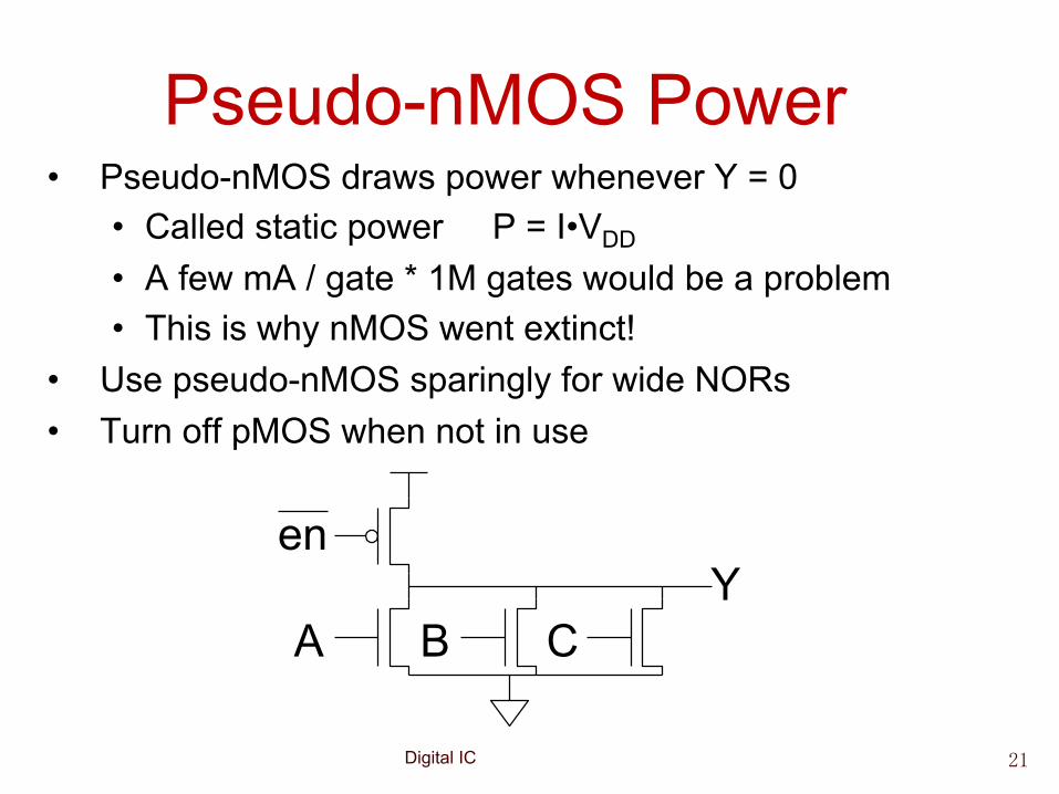
Pseudo-nMOS Power • Pseudo-nMOS draws power whenever Y = 0
• Called static power P = I•VDD
• A few mA / gate * 1M gates would be a problem • This is why nMOS went extinct!
• Use pseudo-nMOS sparingly for wide NORs • Turn off pMOS when not in use
A BY
C
en

Digital IC Introduction EE141
22
Pass-Transistor Logic

Digital IC 23
Pass- transistor logic outline • Pass-transistor principle • Pass-transistor VTC • How to solve pass-transistor threshold drop issue
• Solution 1:Level Restoring Transistor Resistive issue • Solution 2: Single Transistor Pass Gate with VT=0 • Solution 3: Transmission Gate Complementary Pass-
Transistor Logic
• Transmission gate principle
• Some issues of transmission gate
• Resistive issue
• Delay issue

Digital IC 24
Pass-Transistor Logic I n p
u t s Switch
Network
Out Out
A
B
B
B
• N transistors • No static consumption
Pass-transistor logic is a path, not a road connected with rail directly!

Digital IC 25
Example: AND Gate
B
B
A
F = AB
0
Digital IC 26
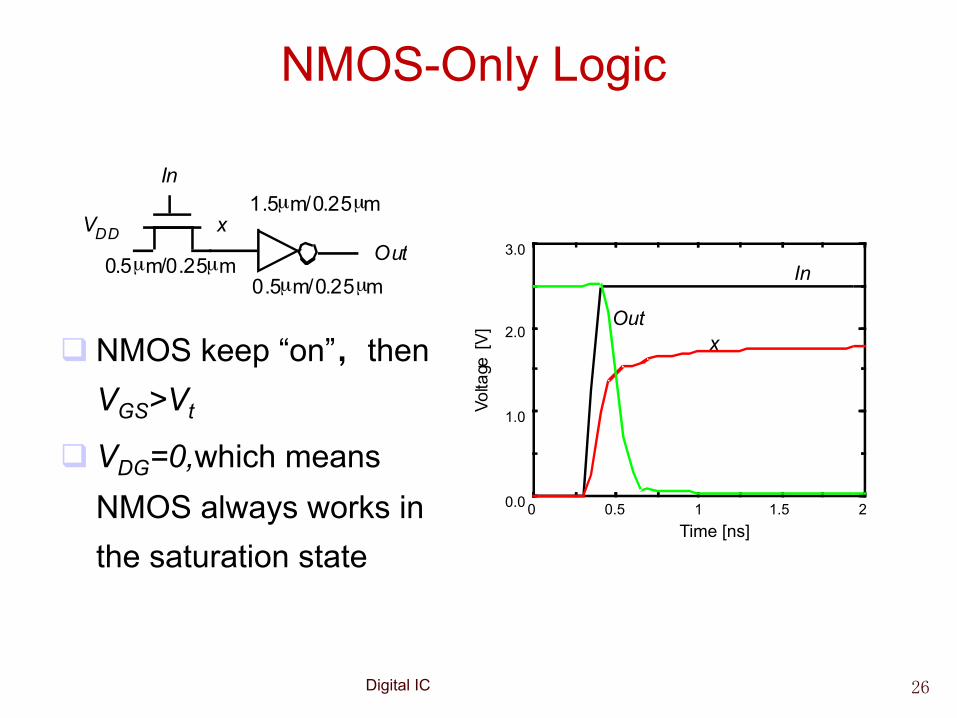
NMOS-Only Logic
VDD
In
Outx
0.5µm/0.25µm0.5µm/0.25µm
1.5µm/0.25µm
0 0.5 1 1.5 2 0.0
1.0
2.0
3.0
Time [ns]
V o l t
a g e [V
]
x Out
In
q NMOS keep “on”,then VGS>Vt
q VDG=0,which means NMOS always works in the saturation state

Digital IC 27
NMOS-only Switch
A = 2.5 V B
C = 2.5 V
C L
A = 2.5 V
C = 2.5 V
B M 2
M 1
M n
Threshold voltage loss causes static power consumption
V B does not pull up to 2.5V, but 2.5V - V TN
NMOS has higher threshold than PMOS (body effect)

Digital IC 28
The proper way of cascading pass gates
• Weak for passing high voltage �
• Proper way of cascading pass transistors,which will not accumulate threshold drop �
{ }DTGs VVVV ,min −=

Digital IC 29
Output of passing-transistor should not be connected with the gate of next stage �

Digital IC Slide 30
Nonrestoring Tristate • Transmission gate acts as tristate buffer
• Only two transistors • But nonrestoring
• Noise on A is passed on to Y
A Y
EN
EN

Digital IC Slide 31
Tristate Inverter • Tristate inverter produces restored output
• Violates conduction complement rule • Because we want a Z output
A
YEN
EN

Digital IC Slide 32
Tristate Inverter • Tristate inverter produces restored output
• Violates conduction complement rule • Because we want a Z output
A
YEN
A
Y
EN = 0Y = 'Z'
Y
EN = 1Y = A
A
EN

Digital IC Slide 33
Gate-Level Mux Design • • How many transistors are needed?
1 0 (too many transistors)Y SD SD= +

Digital IC Slide 34
Gate-Level Mux Design • • How many transistors are needed? 20
1 0 (too many transistors)Y SD SD= +
44
D1
D0S Y
4
2
22 Y
2
D1
D0S

Digital IC Slide 35
Transmission Gate Mux • Nonrestoring mux uses two transmission gates

Digital IC Slide 36
Transmission Gate Mux • Nonrestoring mux uses two transmission gates
• Only 4 transistors
S
S
D0
D1YS

Digital IC Slide 37
Inverting Mux • Inverting multiplexer
• Use compound AOI22 • Or pair of tristate inverters • Essentially the same thing
• Noninverting multiplexer adds an inverter
S
D0 D1
Y
S
D0
D1Y
0
1S
Y
D0
D1
S
S
S
S
S
S

Digital IC Slide 38
4:1 Multiplexer • 4:1 mux chooses one of 4 inputs using two selects
• Two levels of 2:1 muxes • Or four tristates
S0
D0
D1
0
1
0
1
0
1Y
S1
D2
D3
D0
D1
D2
D3
Y
S1S0 S1S0 S1S0 S1S0

Digital IC 39
Pass- transistor logic outline • Pass-transistor principle • Pass-transistor VTC • How to solve pass-transistor threshold drop issue
• Solution 1:Level Restoring Transistor Resistive issue • Solution 2: Single Transistor Pass Gate with VT=0 • Solution 3: Transmission Gate Complementary Pass-
Transistor Logic
• Transmission gate principle
• Some issues of transmission gate
• Resistive issue
• Delay issue

Digital IC 40
Complementary Pass Transistor Logic
A
B
A
B
B B B B
A
B
A
B
F=AB
F=AB
F=A+B
F=A+B
B B
A
A
A
A
F=A⊕ΒÝ
F=A⊕ΒÝ
OR/NOR EXOR/NEXORAND/NAND
F
F
Pass-TransistorNetwork
Pass-TransistorNetwork
AABB
AABB
Inverse
(a)
(b)

Digital IC 41
Pass- transistor logic outline • Pass-transistor principle • Pass-transistor VTC • How to solve pass-transistor threshold drop issue
• Solution 1:Level Restoring Transistor Resistive issue
• Solution 2: Single Transistor Pass Gate with VT=0 • Solution 3: Transmission Gate Complementary Pass-
Transistor Logic • Transmission gate principle
• Some issues of transmission gate
• Resistive issue
• Delay issue

Digital IC 42
Solution 1:Level Restoring Transistor
M 2
M 1
M n
M r
Out A
B
V DD V DD Level Restorer
X
• Advantage: Full Swing • Restorer adds capacitance, takes away pull down current at X • Ratio problem

Digital IC 43
Restorer Sizing
0 100 200 300 400 500 0.0
1.0
2.0
W / L r =1.0/0.25 W / L r =1.25/0.25
W / L r =1.50/0.25 W / L r =1.75/0.25
V o l
t a g e
[V
]
Time [ps]
3.0 • Upper limit on restorer size • Pass-transistor pull-down can have several transistors in stack

Digital IC 44
pass- transistor logic outline • Pass-transistor principle • Pass-transistor VTC • How to solve pass-transistor threshold drop issue
• Solution 1:Level Restoring Transistor Resistive issue • Solution 2: Single Transistor Pass Gate with VT=0 • Solution 3l: Transmission Gate Complementary Pass-
Transistor Logic
• Transmission gate principle
• Some issues of transmission gate
• Resistive issue
• Delay issue

Digital IC 45
Solution 2: Single Transistor Pass Gate with VT=0
Out
V DD
V DD
2.5V
V DD
0V 2.5V
0V
WATCH OUT FOR LEAKAGE CURRENTS

Digital IC 46
pass- transistor logic outline • Pass-transistor principle • Pass-transistor VTC • How to solve pass-transistor threshold drop issue
• Solution 1:Level Restoring Transistor Resistive issue • Solution 2: Single Transistor Pass Gate with VT=0 • Solution 3: Transmission Gate Complementary
Pass-Transistor Logic • Transmission gate principle
• Some issues of transmission gate
• Resistive issue
• Delay issue

Digital IC 47
Solution 3: Transmission Gate
A B
C
C
A B
C
C
B C L
C = 0 V
A = 2.5 V C = 2.5 V

Digital IC 48
pass- transistor logic outline • Pass-transistor principle • Pass-transistor VTC • How to solve pass-transistor threshold drop issue
• Solution 1:Level Restoring Transistor Resistive issue • Solution 2: Single Transistor Pass Gate with VT=0 • Solution 3: Transmission Gate Complementary Pass-
Transistor Logic
• Transmission gate principle • Some issues of transmission gate
• Resistive issue
• Delay issue

Digital IC 49
Pass-Transistor Based Multiplexer
AM2
M1B
S
S
S F
VDD
GND
VDD
In1
In2
S S
S S

Digital IC 50
Transmission Gate XOR
A
B
F
B
A
B
B M1
M2
M3/M4

Digital IC 51
Transmission Gate Full Adder
A
B
P
Ci
VDD A
A A
VDD
Ci
A
P
AB
VDD
VDD
Ci
Ci
Co
S
Ci
P
P
P
P
P
Sum Generation
Carry Generation
Setup
Similar delays for sum and carry

Digital IC 52
pass- transistor logic outline • Pass-transistor principle • Pass-transistor VTC • How to solve pass-transistor threshold drop issue
• Solution 1:Level Restoring Transistor Resistive issue • Solution 2: Single Transistor Pass Gate with VT=0 • Solution 3: Transmission Gate Complementary Pass-
Transistor Logic
• Transmission gate principle
• Some issues of transmission gate • Resistive issue • Delay issue

Digital IC 53
More detail about a processing of low-to-high
• Two transistors stories � • NMOS
• For VGS=VDS , VGD=0<Vt ,then NMOS always works in the saturation or off state �
• PMOS • For VGS=-2.5V, transistor turn
from saturation to linear state � • More detail
linearin offcut :
linearin satur.in :||
saturationin are and |:|
PMOSNMOSVVVPMOSNMOSVVVV
PMOSNMOSVV
outtndd
tnddouttp
tpout
、
、
<−
−<<
<

Digital IC 54
pass- transistor logic outline • Pass-transistor principle • Pass-transistor VTC • How to solve pass-transistor threshold drop issue
• Solution 1:Level Restoring Transistor Resistive issue • Solution 2: Single Transistor Pass Gate with VT=0 • Solution 3: Transmission Gate Complementary Pass-Transistor Logic
• Transmission gate principle
• Some issues of transmission gate • Resistive issue
• Delay issue
• Complementary Pass-Transistor Logic

Digital IC 55
Delay in Transmission Gate Networks �
• Many applications use transmission like that � • Replaced by their equivalent resistances �

Digital IC 56
Computing delay time � • How to do
• Solving the differential equation
• It is too complex to find precise solution,we have to find some approximate solution �
))((111 −+ −−−=
∂
∂iiii
eq
i VVVVCRt
V )(1
,,
1
1
iii
CiiC
IICt
VdtCdV
dtdQIIII
−=∂
∂
==−=
+
+

Digital IC 57
A close solution • Delay time is
• Break chain and Insert buffer 2)1()(τ
0
+==∑
=
nnCRkCRV eq
n
keqn
Digital IC 58
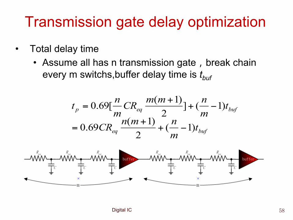
Transmission gate delay optimization
• Total delay time • Assume all has n transmission gate,break chain
every m switchs,buffer delay time is tbuf
bufeq
bufeqp
tmnmnCR
tmnmmCR
mnt
)1(2)1(69.0
)1(]2
)1([69.0
−++
=
−++
=

Digital IC 59
Optimal number of switch moptimal �
0=∂
∂
mtp
02
69.0 2 =−=∂
∂
mntnCR
mt buf
eqp
α== 7171 .CRt
.meq
bufoptimal
It is independent with n