Embed Size (px)
Citation preview
Journal of Microwaves, Optoelectronics and Electromagnetic Applications, Vol. 13, No. 1, June 2014
Brazilian Microwave and Optoelectronics Society-SBMO received 21 Mar 2014; for review 25 Mar 2014; accepted 17 Mar 2014
Brazilian Society of Electromagnetism-SBMag © 2014 SBMO/SBMag ISSN 2179-1074
85
Abstract— In this article, a dual band annular ring patch antenna
is theoretically investigated using the equivalent circuit
concept.Two symmetrical rectangular notches are etched in
radiating ring patch with respect to feed point. It is observed that
the resonant frequency is directly proportional to the notch width
and notch length. The bandwidth of the antenna at lower and
higher ends are 134 MHz(1.815-1.681GHz) and 212MHz (2.849-
2.637GHz) respectively for given antenna specifications. The
calculated results are compared with the IE3D simulation software
and previously reported results based on Artificial Neural Network
(ANN). The theoretical results obtained from the proposed analysis
are in good agreement with the simulated and ANN based results.
Index Terms— Annular ring antenna, Cavity model, Notch loaded ring, dual
band antenna
I. Introduction
Annular Ring Microstrip Antennas (ARMA) have received much attention because of their low
profile, light weight and reduced size suitable for many portable wireless devices [1-2]. The size of
the annular ring patch is smaller than circular or rectangular patch when it resonates in its
fundamental TM11 mode. Annular ring antennas also exhibit broadband nature when operated near
TM12 mode. The radiation efficiency of ring antenna is better than the circular patch antenna because
in ring antenna, the edges at the inner and outer radii causes more fringing while in circular patch
antenna, fringing occurs at the outer edge[3]. In annular ring antennas, the multiband characteristics
can be easily obtained by adjusting the higher modes. A multiple- frequency antenna can reduce the
installation space and provides advantage in cost and size. In the last two decades, many techniques
for the design of patch antennas with multiple frequency operation have been reported such as single
layer shorted pin microstrip antennas [4], gap couple annular ring antennas [5], loading of slots and
notches in the radiating patch [6-9]. The incorporation of suitable dimensions of slot on the circular
patch antenna does not introduce any mode but reduces the second order mode/resonance frequency.
Thus, along with fundamental mode, such perturbed antennas show dualband as well as wideband
behavior [10-12]. Similar properties are also observed in annular ring patch antennas.
Rectangular Notch Loaded Dual Band
Annular Ring Patch Antenna
Prabhakar Singh Department of Physics, Galgotias University, Sector 17-A,Yamuna Expressway,
Greater Noida, Gautam Buddh Nagar-201306,Uttar Pradesh, India
E-mail: [email protected]
Journal of Microwaves, Optoelectronics and Electromagnetic Applications, Vol. 13, No. 1, June 2014
Brazilian Microwave and Optoelectronics Society-SBMO received 21 Mar 2014; for review 25 Mar 2014; accepted 17 Mar 2014
Brazilian Society of Electromagnetism-SBMag © 2014 SBMO/SBMag ISSN 2179-1074
86
Therefore, in this paper, a dual band ARMA has been studied in which two notches are incorporated
in the radiating patch with respect to the feed point. Circuit theory concept is used to analyze the
various antenna characteristics such as impedance bandwidth, return loss,gain and radiation pattern.
The effect of notch dimensions incorporated in the annular ring patch lowers the second order mode
which reduces the separation between the dominant/fundamental and the second order resonating
frequency and hence antenna exhibits a dual frequency nature. The effect of dimensions of rectangular
notches on both upper and lower resonance frequencies has been studied theoretically. After
optimizing the notched annular ring patch the proposed antenna can be used for Global Positioning
System (GPS, 1.575 GHz) and Digital Multimedia Broadcasting (DMB, 2.62 GHz) simultaneously.
II. ANTENNA DESIGN AND ITS EQUIVALENT CIRCUIT
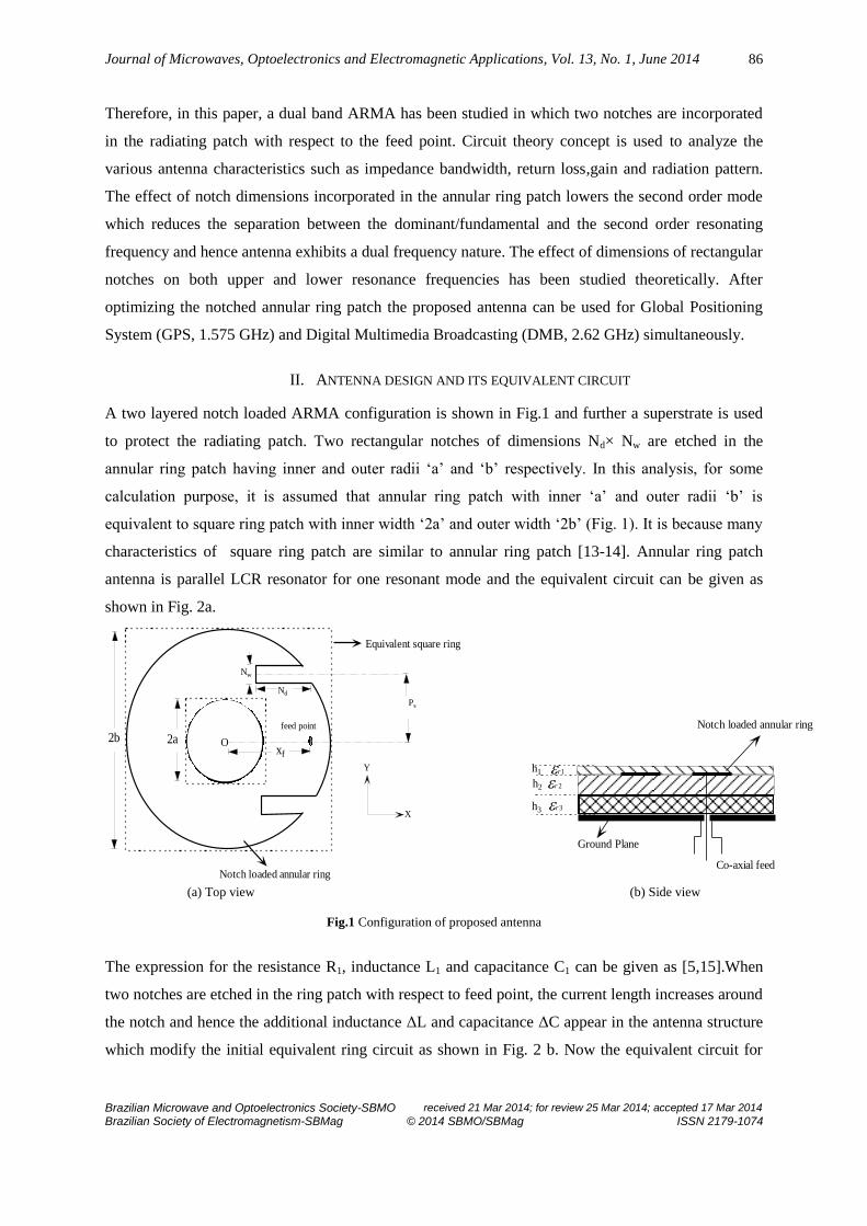
A two layered notch loaded ARMA configuration is shown in Fig.1 and further a superstrate is used
to protect the radiating patch. Two rectangular notches of dimensions Nd× Nw are etched in the
annular ring patch having inner and outer radii ‘a’ and ‘b’ respectively. In this analysis, for some
calculation purpose, it is assumed that annular ring patch with inner ‘a’ and outer radii ‘b’ is
equivalent to square ring patch with inner width ‘2a’ and outer width ‘2b’ (Fig. 1). It is because many
characteristics of square ring patch are similar to annular ring patch [13-14]. Annular ring patch
antenna is parallel LCR resonator for one resonant mode and the equivalent circuit can be given as
shown in Fig. 2a.
Ps
Nw
Nd
Equivalent square ring
Notch loaded annular ring
feed point
xf
2a2b O
Y
X
(a) Top view (b) Side view
Fig.1 Configuration of proposed antenna
The expression for the resistance R1, inductance L1 and capacitance C1 can be given as [5,15].When
two notches are etched in the ring patch with respect to feed point, the current length increases around
the notch and hence the additional inductance ΔL and capacitance ΔC appear in the antenna structure
which modify the initial equivalent ring circuit as shown in Fig. 2 b. Now the equivalent circuit for
Notch loaded annular ring
h3
h1
h2
Co-axial feed
3r
1r2r
Ground Plane
Journal of Microwaves, Optoelectronics and Electromagnetic Applications, Vol. 13, No. 1, June 2014
Brazilian Microwave and Optoelectronics Society-SBMO received 21 Mar 2014; for review 25 Mar 2014; accepted 17 Mar 2014
Brazilian Society of Electromagnetism-SBMag © 2014 SBMO/SBMag ISSN 2179-1074
87
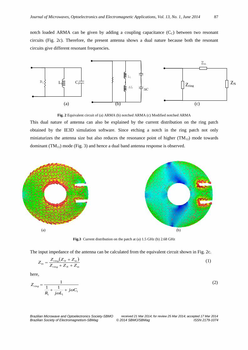
notch loaded ARMA can be given by adding a coupling capacitance (CC) between two resonant
circuits (Fig. 2c). Therefore, the present antenna shows a dual nature because both the resonant
circuits give different resonant frequencies.
(a) (b) (c)
Fig. 2 Equivalent circuit of (a) ARMA (b) notched ARMA (c) Modified notched ARMA
This dual nature of antenna can also be explained by the current distribution on the ring patch
obtained by the IE3D simulation software. Since etching a notch in the ring patch not only
miniaturizes the antenna size but also reduces the resonance point of higher (TM12) mode towards
dominant (TM11) mode (Fig. 3) and hence a dual band antenna response is observed.
(a) (b)
Fig.3 Current distribution on the patch at (a) 1.5 GHz (b) 2.68 GHz
The input impedance of the antenna can be calculated from the equivalent circuit shown in Fig. 2c.
mNring
mNring
inZZZ
ZZZZ
(1)
here,
1
11
11
1
CjLjR
Zring
(2)
C1 L1
R1
Zm
ZN Zring
L1
ΔC ΔL
Journal of Microwaves, Optoelectronics and Electromagnetic Applications, Vol. 13, No. 1, June 2014
Brazilian Microwave and Optoelectronics Society-SBMO received 21 Mar 2014; for review 25 Mar 2014; accepted 17 Mar 2014
Brazilian Society of Electromagnetism-SBMag © 2014 SBMO/SBMag ISSN 2179-1074
88
2
22
11
1
CjLjR
ZN
(3)
in which, LLL 12 and
CC
CCC
1
12
The additional inductance (ΔL) and capacitance (ΔC) can be calculated by [16-17]
c
mCj
Z
1 (4)
where, CC is the coupling capacitance and given by [18]
2
)/11()()( 2
21
2
2121 c
c
kCCCCCCC
in which, 21
1
QQkc
here Q1 and Q2 are the quality factors of both the resonators. The resonance resistance (R2) of the
modified configuration of the ARMA can be calculated from [19]. In the proposed antenna three
layers of dielectric substrates are used, the effective dielectric constant of the structure can be
calculated from [20]. The values of reflection coefficient and return loss can be calculated as:
Reflection Coefficient ( ) =in
in
ZZ
ZZ
0
0 (5)
where Z0= characteristic impedance of coaxial feed (50 )
Return loss = -20 log10 ( ) (6)
The radiation pattern for the antenna can be given by assuming it as conventional annular ring antenna
[21].
nbkJbkJ
akJakJ
rk
eEhkjE n
nmn
nmnn
nm
rjkn
cos)].sin()(
)()sin([
20
'
'
'
0
'000
(7)
n
bk
bkJ
bkJ
akJ
ak
akJ
rk
eEhkjE n
nmn
nmnn
nm
rjkn
sincos].sin
)sin(
)(
)(
sin
)sin([
2
0
0
'
'
0
0000
(8)
Here r is the distance of an arbitrary far field point, k0 and knm are the propagation constants in free
space and in dielectric medium in TMnm mode respectively.
Journal of Microwaves, Optoelectronics and Electromagnetic Applications, Vol. 13, No. 1, June 2014
Brazilian Microwave and Optoelectronics Society-SBMO received 21 Mar 2014; for review 25 Mar 2014; accepted 17 Mar 2014
Brazilian Society of Electromagnetism-SBMag © 2014 SBMO/SBMag ISSN 2179-1074
89
III. CALCULATION AND DISCUSSION OF RESULTS
TABLE 1. DESIGN SPECIFICATIONS FOR THE ANTENNA
Parameters Values
Dielectric constant of material used for thickness h1=6.1 mm =1.03
Dielectric constnat of material used for thickness h2=6.05 mm =3.5
Dielectric constant of material used for thickness h3=1.1 mm =1.04
Inner radius of the ring (a) 12.05 mm
Outer radius of the ring (b) 36.10 mm
Length of the notch (Nd) 15mm
Width of the notch (Nw) 3.0 mm
Feed location (x0,y0) 27.0,0 mm
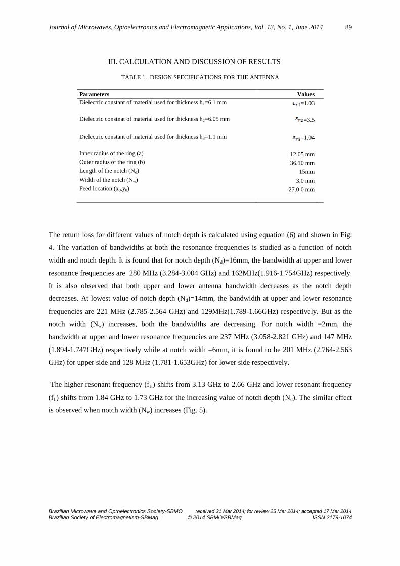
The return loss for different values of notch depth is calculated using equation (6) and shown in Fig.
4. The variation of bandwidths at both the resonance frequencies is studied as a function of notch
width and notch depth. It is found that for notch depth (Nd)=16mm, the bandwidth at upper and lower
resonance frequencies are 280 MHz (3.284-3.004 GHz) and 162MHz(1.916-1.754GHz) respectively.
It is also observed that both upper and lower antenna bandwidth decreases as the notch depth
decreases. At lowest value of notch depth (Nd)=14mm, the bandwidth at upper and lower resonance
frequencies are 221 MHz (2.785-2.564 GHz) and 129MHz(1.789-1.66GHz) respectively. But as the
notch width (Nw) increases, both the bandwidths are decreasing. For notch width =2mm, the
bandwidth at upper and lower resonance frequencies are 237 MHz (3.058-2.821 GHz) and 147 MHz
(1.894-1.747GHz) respectively while at notch width =6mm, it is found to be 201 MHz (2.764-2.563
GHz) for upper side and 128 MHz (1.781-1.653GHz) for lower side respectively.
The higher resonant frequency (fH) shifts from 3.13 GHz to 2.66 GHz and lower resonant frequency
(fL) shifts from 1.84 GHz to 1.73 GHz for the increasing value of notch depth (Nd). The similar effect
is observed when notch width (Nw) increases (Fig. 5).
Journal of Microwaves, Optoelectronics and Electromagnetic Applications, Vol. 13, No. 1, June 2014
Brazilian Microwave and Optoelectronics Society-SBMO received 21 Mar 2014; for review 25 Mar 2014; accepted 17 Mar 2014
Brazilian Society of Electromagnetism-SBMag © 2014 SBMO/SBMag ISSN 2179-1074
90
Fig.4 Variation of return loss with frequency for different notch depth (Nd)
Fig.5 Variation of return loss with frequency for different notch width (Nw)
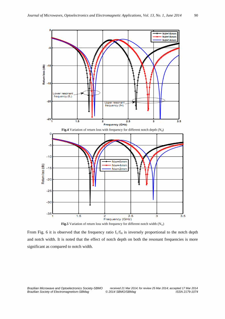
From Fig. 6 it is observed that the frequency ratio fL/fH is inversely proportional to the notch depth
and notch width. It is noted that the effect of notch depth on both the resonant frequencies is more
significant as compared to notch width.
Journal of Microwaves, Optoelectronics and Electromagnetic Applications, Vol. 13, No. 1, June 2014
Brazilian Microwave and Optoelectronics Society-SBMO received 21 Mar 2014; for review 25 Mar 2014; accepted 17 Mar 2014
Brazilian Society of Electromagnetism-SBMag © 2014 SBMO/SBMag ISSN 2179-1074
91
Fig.6 Variation of frequency ratio with different notch depth (Nd) and notch width (Nw)
Fig.7 Comparative results of return loss with frequency of the ARMA for proposed, simulated and ANN method
Journal of Microwaves, Optoelectronics and Electromagnetic Applications, Vol. 13, No. 1, June 2014
Brazilian Microwave and Optoelectronics Society-SBMO received 21 Mar 2014; for review 25 Mar 2014; accepted 17 Mar 2014
Brazilian Society of Electromagnetism-SBMag © 2014 SBMO/SBMag ISSN 2179-1074
92
(a)
(b)
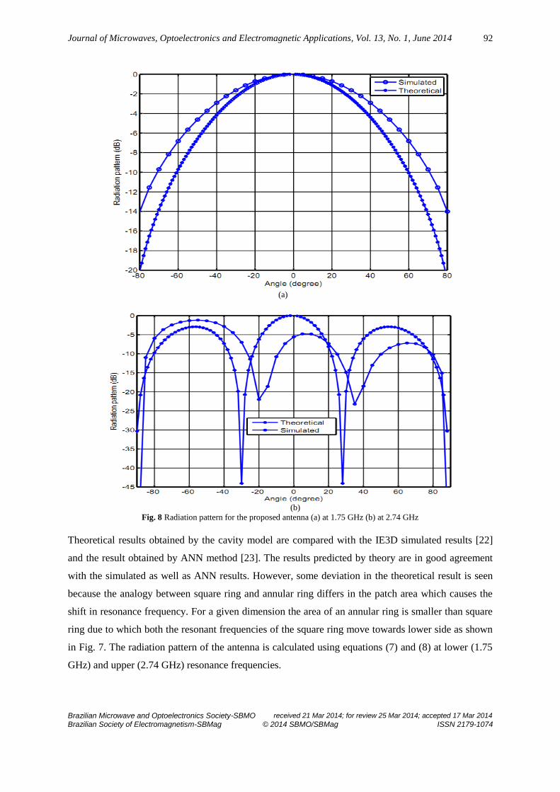
Fig. 8 Radiation pattern for the proposed antenna (a) at 1.75 GHz (b) at 2.74 GHz
Theoretical results obtained by the cavity model are compared with the IE3D simulated results [22]
and the result obtained by ANN method [23]. The results predicted by theory are in good agreement
with the simulated as well as ANN results. However, some deviation in the theoretical result is seen
because the analogy between square ring and annular ring differs in the patch area which causes the
shift in resonance frequency. For a given dimension the area of an annular ring is smaller than square
ring due to which both the resonant frequencies of the square ring move towards lower side as shown
in Fig. 7. The radiation pattern of the antenna is calculated using equations (7) and (8) at lower (1.75
GHz) and upper (2.74 GHz) resonance frequencies.
Journal of Microwaves, Optoelectronics and Electromagnetic Applications, Vol. 13, No. 1, June 2014
Brazilian Microwave and Optoelectronics Society-SBMO received 21 Mar 2014; for review 25 Mar 2014; accepted 17 Mar 2014
Brazilian Society of Electromagnetism-SBMag © 2014 SBMO/SBMag ISSN 2179-1074
93
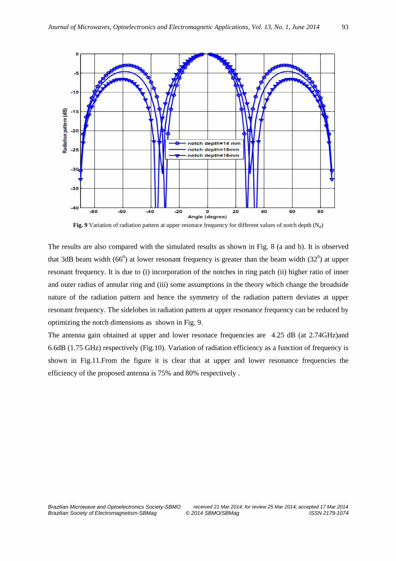
Fig. 9 Variation of radiation pattern at upper resonace frequency for different values of notch depth (Nd)
The results are also compared with the simulated results as shown in Fig. 8 (a and b). It is observed
that 3dB beam width (660) at lower resonant frequency is greater than the beam width (32
0) at upper
resonant frequency. It is due to (i) incorporation of the notches in ring patch (ii) higher ratio of inner
and outer radius of annular ring and (iii) some assumptions in the theory which change the broadside
nature of the radiation pattern and hence the symmetry of the radiation pattern deviates at upper
resonant frequency. The sidelobes in radiation pattern at upper resonance frequency can be reduced by
optimizing the notch dimensions as shown in Fig. 9.
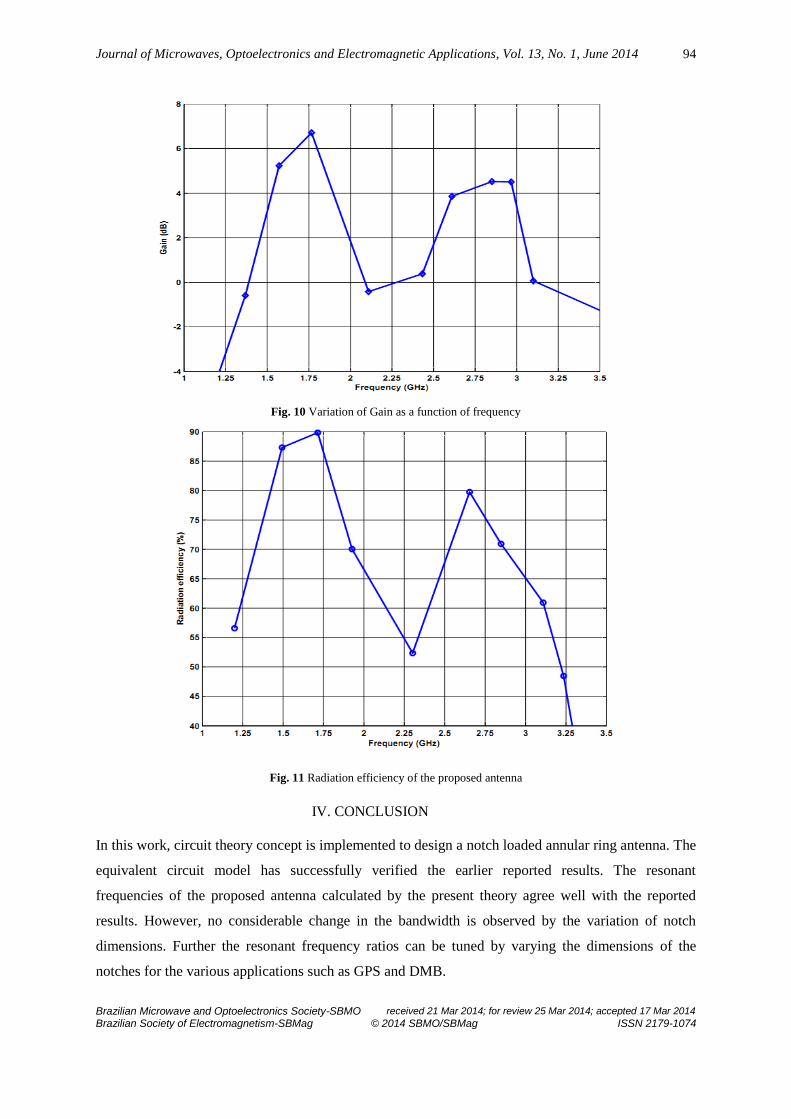
The antenna gain obtained at upper and lower resonace frequencies are 4.25 dB (at 2.74GHz)and
6.6dB (1.75 GHz) respectively (Fig.10). Variation of radiation efficiency as a function of frequency is
shown in Fig.11.From the figure it is clear that at upper and lower resonance frequencies the
efficiency of the proposed antenna is 75% and 80% respectively .
Journal of Microwaves, Optoelectronics and Electromagnetic Applications, Vol. 13, No. 1, June 2014
Brazilian Microwave and Optoelectronics Society-SBMO received 21 Mar 2014; for review 25 Mar 2014; accepted 17 Mar 2014
Brazilian Society of Electromagnetism-SBMag © 2014 SBMO/SBMag ISSN 2179-1074
94
Fig. 10 Variation of Gain as a function of frequency
Fig. 11 Radiation efficiency of the proposed antenna IV. CONCLUSION
In this work, circuit theory concept is implemented to design a notch loaded annular ring antenna. The
equivalent circuit model has successfully verified the earlier reported results. The resonant
frequencies of the proposed antenna calculated by the present theory agree well with the reported
results. However, no considerable change in the bandwidth is observed by the variation of notch
dimensions. Further the resonant frequency ratios can be tuned by varying the dimensions of the
notches for the various applications such as GPS and DMB.
Journal of Microwaves, Optoelectronics and Electromagnetic Applications, Vol. 13, No. 1, June 2014
Brazilian Microwave and Optoelectronics Society-SBMO received 21 Mar 2014; for review 25 Mar 2014; accepted 17 Mar 2014
Brazilian Society of Electromagnetism-SBMag © 2014 SBMO/SBMag ISSN 2179-1074
95
REFERENCES
[1] R. Garg and V. S. Reddy, “Edge feeding of microstrip ring antennas,” IEEE Transactions on Antennas and
Propagation, vol.51, no.8, pp.1941-1946, 2003.
[2] D.M. Kokotoff , J. T. Aberle and R. B. Waterhouse, “Rigorous analysis of probe fed printed annular ring
antennas,” IEEE Transactions on Antennas and Propagation, vol. 47, no.2, pp.384-388, 1999.
[3] Ouarda Barkat, “Full-Wave Spectral Analysis of Resonant Characteristics and Radiation Patterns of
High Tc Superconducting Circular and Annular Ring Microstrip Antennas” in Advancement in
Microstrip Antennas with Recent Applications, InTech Publication, Croatia, pp. 57, 2013.
[4] S. C. Pan and K. L. Wong, “Design of dual-frequency microstrip antennas using a shorting-pin loading,” IEEE
International Symposium, vol.1, pp.312-315, 21-26 June, 1998. [5] B.K. Kanaujiya and A.K. Singh, “Analysis and design of gap-coupled annular ring Microstrip antennas,”
International Journal of Antennas and Propagation, doi:10.1155/2008/792123, 2008.
[6] Y. M. M. Antar , A. I. Ittip Iboon and A. K. Bhattachatyya, “A dual-frequency antenna using a single patch and an
inclined slot,” Microw. and Opt. Technol. Lett., vol. 8, no.6, pp.309-310,1995.
[7] K. F. Lee, K. M. Luk, K. M. Mak and S. L. S.Yang, “On the use of U-slots in the design of dual-and triple-band
patch antennas,” IEEE Transactions on Antennas and Propagation, vol.53, no.3, pp.60-74,2011.
[8] J. S. Chen, “ Multi-frequency characteristics of annular-ring slot antennas,” Microw. Opt. Technol. Lett., vol.38,
pp.506–511,2003.
[9] X.C. Yin, C.L. Ruan, S.G. Mo, C.Y. Ding, and J.H. Chu, “A compact ultra- wideband microstrip antenna with
multiple notches," Progress In Electromagnetics Research , vol. 84, pp.321332, 2008.
[10] A.A. Deshmukh, K.P. Ray, T. Sonawdeker, S. Warawalla and R. Kataria, “ Formulation of resonance frequency
for multiband circular Microstrip antennas,” Int. Journal of Microw. and Optical Technology, vol. 5, no.5, pp. 248-
256,2010.
[11] R. Azim, M. T. Islam, J. S. Mandeep and A. T. Mobashsher, “A planar circular ring ultra-wideband antenna with
dual band-notched characteristics”, Journal of Electromagnetic Waves and Applications, vol. 26, nos. 14–15, pp.
2022–2032, 2012.
[12] R. Azim, M. T. Islam and N. Misran, “Printed circular disc compact planar antenna for UWB applications”,
Telecommunication Systems, vol. 52, no. 2, pp. 1171-1177, 2013.
[13] S. H. Chen, J. S. Row and C. Y. D. Sim, “Single-feed square- ring patch antenna with dual-frequency operation,”
Microwave and Optical Technology Letters, vol. 49, pp. 991-994, 2007.
[14] S. Behera and K. J. Vinoy “Resonance characteristics of non-uniform width square ring antennas,” Progress In
Electromagnetics Research C, vol. 31, pp.54-66, 2012.
[15] A. K. Bhattacharyya and R. Garg, “ A Microstrip array of concentric annular rings,” IEEE Transactions on
Antennas and Propagation, vol.33, no. 6, pp.655-659, 1985.
[16] X. X. Zhang and F. Yang, “Study of a slit cut on a microstrip antenna and its applications,” Microw. Opt.
Technol. Lett., vol. 18, pp. 297-300, 1998.
[17] I. J. Bahal, “ Lumped elements for RF and microwave circuits,” Artech House, Boston, pp. 456-459, 2003.
[18] V. K. Pandey and B. R. Vishvakarma, “ Analysis of an E-shaped patch antenna,” Microw. Opt. Technol. Lett., vol.
49,no.1, pp. 4-1,2007.
[19] C. A.Balanis, “ Antenna theory analysis and design,” 2nd edition, New York, Wiely, pp. 728-746,1997.
[20] S. Jiri, “Analysis of multilayer microstrip lines by a conformal mapping method,” IEEE Trans Microw. Theory
and Tech., vol. 40, pp.769-772,1992.
Journal of Microwaves, Optoelectronics and Electromagnetic Applications, Vol. 13, No. 1, June 2014
Brazilian Microwave and Optoelectronics Society-SBMO received 21 Mar 2014; for review 25 Mar 2014; accepted 17 Mar 2014
Brazilian Society of Electromagnetism-SBMag © 2014 SBMO/SBMag ISSN 2179-1074
96
[21] R.Garg, P. Bhartia, I. Bahl and A. Ittipiboon, “Microstrip Antenna Design Handbook,” Artech House, Norwood,
MA,2001.
[22] IE3D simulation software, Zeland, version 14.05, 2008.
[23] K. Siakavara, “Artificial Neural Network employment in the design of multilayered microstrip antenna with
specified frequency operation,” PIERS Online, vol. 3, pp.1278-1282, 2007.