Embed Size (px)
Citation preview

Reducing Film Thickness in Lead Zirconate Titanate
Thin Film Capacitors
by Vikram Rao and Ronald G. Polcawich
ARL-TR-4338 December 2007 Approved for public release; distribution is unlimited.

NOTICES
Disclaimers The findings in this report are not to be construed as an official Department of the Army position unless so designated by other authorized documents. Citation of manufacturer’s or trade names does not constitute an official endorsement or approval of the use thereof. Destroy this report when it is no longer needed. Do not return it to the originator.

Army Research Laboratory Adelphi, MD 20783-1197
ARL-TR-4338 December 2007
Reducing Film Thickness in Lead Zirconate Titanate Thin Film Capacitors
Vikram Rao and Ronald G. Polcawich
Sensors and Electron Devices Directorate, ARL Approved for public release; distribution is unlimited.

ii
REPORT DOCUMENTATION PAGE Form Approved OMB No. 0704-0188
Public reporting burden for this collection of information is estimated to average 1 hour per response, including the time for reviewing instructions, searching existing data sources, gathering and maintaining the data needed, and completing and reviewing the collection information. Send comments regarding this burden estimate or any other aspect of this collection of information, including suggestions for reducing the burden, to Department of Defense, Washington Headquarters Services, Directorate for Information Operations and Reports (0704-0188), 1215 Jefferson Davis Highway, Suite 1204, Arlington, VA 22202-4302. Respondents should be aware that notwithstanding any other provision of law, no person shall be subject to any penalty for failing to comply with a collection of information if it does not display a currently valid OMB control number. PLEASE DO NOT RETURN YOUR FORM TO THE ABOVE ADDRESS. 1. REPORT DATE (DD-MM-YYYY)
December 2007 2. REPORT TYPE
Final 3. DATES COVERED (From - To)
May 2007 to July 2007 5a. CONTRACT NUMBER
5b. GRANT NUMBER
4. TITLE AND SUBTITLE
Reducing Film Thickness in Lead Zirconate Titanate Thin Film Capacitors
5c. PROGRAM ELEMENT NUMBER
5d. PROJECT NUMBER
5e. TASK NUMBER
6. AUTHOR(S)
Vikram Rao and Ronald G. Polcawich
5f. WORK UNIT NUMBER
7. PERFORMING ORGANIZATION NAME(S) AND ADDRESS(ES)
U.S. Army Research Laboratory ATTN: AMSRD-ARL-SE-RL 2800 Powder Mill Road Adelphi, MD 20783-1197
8. PERFORMING ORGANIZATION REPORT NUMBER
ARL-TR-4338
10. SPONSOR/MONITOR'S ACRONYM(S)
9. SPONSORING/MONITORING AGENCY NAME(S) AND ADDRESS(ES)
11. SPONSOR/MONITOR'S REPORT NUMBER(S)
12. DISTRIBUTION/AVAILABILITY STATEMENT
Approved for public release; distribution is unlimited.
13. SUPPLEMENTARY NOTES
14. ABSTRACT
The goal of this project is to characterize the dielectric and ferroelectric performance of lead zirconate titanate (PZT) thin film capacitors as a function of film thickness and sol-gel solution composition. For the thickness experiments, the underlying silicon dioxide, platinum electrode, and the spin-deposited PZT thicknesses were varied. For the solution tests, the molarity and the zirconium/titanium ratio was also varied. In addition, PZT spin rate was varied to determine the spin rate’s effect on PZT thickness and dielectric and ferroelectric properties. Both capacitance and hysteresis data were taken for all samples. This project will aid the Defense Advanced Research Projects Agency (DARPA) nanoelectromechanical switch (NEMS) program by investigating avenues of reducing film thickness while maintaining acceptable levels of performance.
15. SUBJECT TERMS
PZT, Thin Film, Ferroelectric, Capacitors
16. SECURITY CLASSIFICATION OF: 19a. NAME OF RESPONSIBLE PERSON
Ronald G. Polcawich a. REPORT
U b. ABSTRACT
U c. THIS PAGE
U
17. LIMITATION OF ABSTRACT
SAR
18. NUMBER OF PAGES
24 19b. TELEPHONE NUMBER (Include area code)
(301) 394-1275 Standard Form 298 (Rev. 8/98) Prescribed by ANSI Std. Z39.18

Contents
List of Figures iv
List of Tables iv
Acknowledgments v
1. Introduction 1 1.1 Motivation .......................................................................................................................1
1.2 Ferroelectric Property of PZT .........................................................................................1
2. Experiment and Calculations 2 2.1 Sample Preparation..........................................................................................................2
2.2 Tests and Test Equipment ...............................................................................................5
2.3 Procedure.........................................................................................................................6 2.3.1 Dielectric and Ferroelectric Tests........................................................................6 2.3.2 Sol-gel PZT Solution Test ...................................................................................6
2.4 Calculations .....................................................................................................................6
3. Results and Discussion 7 3.1 Thickness Tests ...............................................................................................................7
3.2 Spin Rate Test ...............................................................................................................10
4. Summary and Conclusion 14
Symbols, Abbreviations, and Acronyms 15
Distribution List 16
iii
List of Figures
Figure 1. Typical P-E ferroelectric hysteresis loop. ...................................................................... 2 Figure 2. Wet-etched region (bottom Pt electrode). ...................................................................... 5 Figure 3. Test capacitor (top Pt electrode)..................................................................................... 5 Figure 4. Ferroelectric and dielectric test results for wafer 2151. ................................................. 7 Figure 5. Ferroelectric and dielectric test results for wafer 2174. ................................................. 8 Figure 6. Ferroelectric and dielectric test results for wafer 2156. ................................................. 9 Figure 7. Selected hysteresis loops for wafer 2156. .................................................................... 10 Figure 8. Thicknesses after 1 spin for various spin rates and PZT sol-gel solutions................... 11 Figure 9. Thicknesses by spin for sol-gel solution 190. .............................................................. 12 Figure 10. Thicknesses by spin for sol-gel solution 192. ............................................................ 13
List of Tables
Table 1. Varying substrate layer thicknesses................................................................................. 2 Table 2. Varying PZT thicknesses. ................................................................................................ 3 Table 3. Final PZT thicknesses for spin rate test. .......................................................................... 4 Table 4. Various sol-gel PZT solutions. ........................................................................................ 5 Table 5. Sol-gel PZT solution test results.................................................................................... 14
iv

Acknowledgments
The authors would like to thank Gregory Chevis and Joel Martin from General Technical Services for their work in preparing the thin film lead zirconate titanate (PZT) samples. We would also like to thank Richard Piekarz, U.S. Army Research Laboratory (ARL) for assisting in the preparation of the measurement test equipment.
v

vi
INTENTIONALLY LEFT BLANK.

1. Introduction
1.1 Motivation
The purpose of this project was to investigate the effect of reducing the thickness of the dielectric, platinum electrode layers, and lead zirconate titanate (PZT) thin film in PZT ferroelectric capacitors. To test the nature of this relationship, capacitance and ferroelectric data were taken from three sample wafers with varying layer thicknesses on each wafer. Another set of testing was conducted to investigate the performance of different PZT solution molarities and spin rate on PZT film thickness and the ferroelectric and dielectric characteristics of the PZT capacitors. The results from this project will provide critical information to the Defense Advanced Research Projects Agency (DARPA) funded nanoelectromechanical system (NEMS) switch program. The goal of the NEMS program is to create switches small enough to be combined with complementary metal-oxide semiconductor (CMOS) transistors to improve the leakage power of the transistor.
1.2 Ferroelectric Property of PZT
PZT is a ceramic with chemical formula Pb[ZrxTi1-x]O3, which is frequently employed as a capacitor dielectric because of its ferroelectric properties. In addition to a high dielectric constant, a ferroelectric material possesses a spontaneous polarization that can be switched by a strong external electric field. A related phenomenon is the tendency for ferroelectrics to exhibit a polarization hysteresis as a function of applied electric field. A typical hysteresis loop plots a ferroelectric sample’s net polarization against the applied electric field. The critical features, shown in Figure 1, are the remanent polarization Pr
+ and Pr-, which describes the remaining net
polarizations when the field is brought back to a zero electric field, for both positively and negatively poled samples. For this research, the capacitance and ferroelectric hysteresis loop characteristics will be measured as a function of PZT film thickness and as a function of underlying metal and dielectric thin film thicknesses.
1

Figure 1. Typical P-E ferroelectric hysteresis loop.1
2. Experiment and Calculations
2.1 Sample Preparation
For the first test, all wafers were fabricated beginning with 100 mm silicon substrates followed by conformal deposition of silicon dioxide (SiO2), titanium (Ti), platinum (Pt), and PZT thin films of varying thickness. The layer thicknesses for each of the tested wafer samples can be found in tables 1 and 2.
Table 1. Varying substrate layer thicknesses.
Wafer ID SiO2 (Å) Ti (Å) Pt (Å) 2151 2251 200 820 2174 2251 50 500 2156 165 50 500
1 Adapted from Jaffe, B.; Cook, W.R.; Jaffe, H. Piezoelectric Ceramics, R.A.N., Ohio, 1971.
2

Table 2. Varying PZT thicknesses.
Sample Number of PZT Spins Thickness (µm)
2151-1A 8 0.3966 2151-1B 7 0.3332 2151-1C 6 0.2873 2151-1D 5 0.2367 2151-1E 4 0.1869 2151-1F 3 0.1359 2151-1G 2 0.0808 2151-1H 1 0.0461
2174-3A 8 0.38471 2174-3B 7 0.33446 2174-3C 6 0.28483 2174-3D 5 0.23894 2174-3E 4 0.18189 2174-3F 3 0.13815 2174-3G 2 0.14456 2174-3H 1 0.04483
2156-5A 8 0.3893 2156-5B 7 0.33912 2156-5C 6 0.28835 2156-5D 5 0.24164 2156-5E 4 0.18686 2156-5F 3 0.15315 2156-5G 2 0.14456 2156-5H 1 0.044762
The SiO2 thin films were deposited by plasma enhanced chemical vapor deposition followed by a rapid thermal anneal at 700 ºC in 5 standard cubic centimeters per minute (sccm) of flowing nitrogen (N2) for 60 s. The Ti and Pt films were deposited by direct current (DC) magnetron sputtering at 500 ºC with the Pt thin film deposited immediately following the Ti thin film without exposing the wafer to the ambient conditions. Following the metal deposition, the wafer was cleaved into eight samples approximately 1.5 cm × 1.5 cm in area. Each sample was coated with sol-gel PZT thin films of varying thickness from 1 to 8 spin layers. Each PZT layer was spin-deposited at 3000 revolutions per minute (rpm) for 30 s. After spinning, the samples were placed onto a hot plate at 350 °C for 2 min to remove the volatile organics. The sample was then cooled on small piece of aluminum. Finally, the PZT was crystallized using a rapid thermal anneal (RTA) at 700 ºC for 30 s in flowing compressed dry air. After the wafer was cooled to room temperature, 1050 Å of Pt was sputter deposited onto the sample surface at 300 ºC. Following the Pt deposition, the process to define the PZT thin film capacitors began by coating
3

the sample with 5214-E photoresist. The photoresist was patterned with an array of 500 μm × 500 μm squares of resist.
After developing the photoresist, the samples underwent a 2 min oxygen plasma descumming process to remove photoresist residues. Next, the resist was cured using a combination of ultraviolet (UV) illumination and temperature (220 ºC). The UV-cured resist helps prevent heavy metal ion implantation that can occur during the argon ion-milling process used to remove undesired regions of Pt on top of the PZT. Following the ion-milling process, the remaining resist was removed with a 25 min oxygen plasma. To open a window to the bottom Pt, another layer of resist was coated onto the sample. Next, a corner of the sample was wiped clean with acetone to remove the photoresist. Subsequently, this corner was exposed to a wet-etch bath consisting of H2O:HCl:HF (2:1:0.05) to etch the PZT revealing the underlying platinum layer. Following the wet etch of PBT, the resist is removed using Acetone. Next, the samples undergo a rapid thermal anneal at 350 °C in 5 sccm of flowing compressed dry air for 120 s. The anneal serves to remove any sputter induced surface damage and improve the PBT interface.
For the spin rate test, the process was varied slightly: 100 Å of Ti and 850 Å of Pt were sputtered onto the silicon dioxide coated wafer at 300 ºC. The wafers were cleaved into 1.5 cm × 1.5 cm samples to create a total of 15 test specimens. These specimens were then coated with either sol-gel PZT solution 190, 191, or 192 and spun to a PZT thickness of ~ 4000 Å at spin rates of 1, 2, 3, 4, and 5 krpm (kilo rotations per minute). The actual thicknesses are located in table 3. The remainder of the sample preparation process was similar to that of the thickness tests except that the spin rate samples did not undergo descumming or ion milling to define the top Pt metallization. Instead the top Pt was patterned using a photoresist liftoff process using Pt sputter deposited at room temperature.
Table 3. Final PZT thicknesses for spin rate test.
Sol-gel PZT Solution 1000 rpm 2000 rpm 3000 rpm 4000 rpm 5000 rpm
190 4051.5 Å 3871.5 Å 4419.4 Å 3977.5 Å 3786.6 Å 191 Bad Sample Bad Sample Bad Sample Bad Sample Bad Sample 192 4636.5 Å 3749.2 Å 4596.1 Å 4102.4 Å 3903.4 Å
For the PZT solution test, three different samples with varying sol-gel PZT solutions were prepared using the same process as the thickness test. The solutions varied in their zirconium (Zr) to Ti ratio and overall molarity. Table 4 gives the exact solution composition.
4

Table 4. Various Sol-gel PZT solutions.
Sol-gel PZT Solution Zr/Ti Ratio Molarity
(M) Test Sample
Thickness (µm) 190 45/55 .367 0.5246 191 45/55 .12 0.39724
191 (2221) 45/55 .12 0.19022 192 52/48 .587 0.80973
2.2 Tests and Test Equipment
The capacitance measurements were taken with a Hewlett-Packard 4275A LCR meter. The ferroelectric measurements were taken with the Radiant Technologies RT-66i ferroelectric test setup, which works by stepping though a series of voltages in a triangular bipolar waveform. At each step, the current induced in the sample is integrated to obtain a charge, which combined with sample area information, is used to calculate polarization. For these tests, a pair of micromanipulators or probes are used to make contact with the bottom and top platinum layers as shown in figures 2 and 3.
Probe (-)
500 µm
Figure 2. Wet-etched region (bottom Pt electrode).
Probe (+)
500 µm
Figure 3. Test capacitor (top Pt electrode).
5

2.3 Procedure
2.3.1 Dielectric and Ferroelectric Tests
The first test investigated the properties of the capacitors as a function of PZT thickness. Both dielectric and ferroelectric measurements were taken from each wafer for samples of varying numbers of PZT spin depositions (varying thicknesses). Micromanipulator probes were contacted with the exposed bottom Pt and individual top Pt terminal of each capacitor. Using the LCR meter, capacitance measurements and dielectric loss tangents were taken at 10 kHz with a 50 mVAC input signal. A hysteresis loop was then obtained using the ferroelectric test equipment. The setup required input of the capacitor’s area, thickness, and desired peak voltage to run the hysteresis test. All capacitors had an area of 0.0025 cm2. The peak voltage was normalized against film thickness (8 spins: 19V, 7 spins: 16.625V, 6 spins: 14.250V, etc.) to ensure a somewhat constant electric field. Dielectric and ferroelectric tests were repeated for eight test capacitors on each sample to obtain mean and standard deviation values.
2.3.2 Sol-gel PZT Solution Test
The second test investigated the dielectric and ferroelectric properties of samples spun with the different PZT solutions (190, 191, and 192). The same testing procedure was used with the peak voltage of the ferroelectric test once again being normalized against thickness, which was different between the samples. Dielectric and ferroelectric tests were repeated for eight test capacitors on each sample.
2.4 Calculations
The dielectric constant was calculated for each capacitor using equation 1, where C is capacitance, t is film thickness, and A is capacitor area.
AtC⋅⋅
=0ε
ε (1)
6

3. Results and Discussion
3.1 Thickness Tests
Wafer 2151 yielded usable results from 8 to 4 spins of PZT. At 4 spins, remanent polarizations were 14.74 and -14.43 μC/cm2, for the two polarization states, and the dielectric constant was 844, within the acceptable range (800-1200), see figure 4. At 3 spins (sample 1F), however, both remanent polarizations (10.30 and –10.92 μC/cm2) and dielectric constant (457) dropped sharply.
Polarization & Dielectric Constant vs. Thickness
-25
-20
-15
-10
-5
0
5
10
15
20
25
0 0.05 0.1 0.15 0.2 0.25 0.3 0.35 0.4 0.45
Thickness (µm)
Pola
rizat
ion
(µC
/cm
2 )
0
200
400
600
800
1000
1200
1400
1600
1800
2000
Die
lect
ric C
onst
ant
PrPr-Dielectric Constant
Figure 4. Ferroelectric and dielectric test results for wafer 2151.
NOTE: 1-σ error bars included, but obscured by data point icons.
7

Wafer 2174, where the Ti and bottom Pt layers were thinned compared to wafer 2151, exhibited a similar trend of decreasing polarizations and dielectric constants with decreasing thickness except for the 3 spin sample (3F), see figure 5. At 1382 Å, this capacitor provided acceptable polarizations although its dielectric constant values were slightly lower than the desired value of 800.
Polarization & Dielectric Constant vs. Thickness
-25
-20
-15
-10
-5
0
5
10
15
20
25
0 0.05 0.1 0.15 0.2 0.25 0.3 0.35 0.4 0.45
Thickness (µm)
Pola
rizat
ion
(µC
/cm
2 )
0
100
200
300
400
500
600
700
800
900
1000
Die
lect
ric C
onst
ant
PrPr-Dielectric Constant
Figure 5. Ferroelectric and dielectric test results for wafer 2174.
NOTE: 1-σ error bars included, but obscured by data point icons.
8

Wafer 2156 also yielded similar performance trends as the other two wafers, but also had anomalously well-performing capacitors at 4 spins, at a thickness of 1869 Å, see figure 6. This capacitor had polarizations well over 20 μC/cm2, along with a dielectric constant in the range of 800. Further testing is ongoing to assess the validity of the 4 spin data.
Polarization & Dielectric Constant vs. Thickness
-30
-25
-20
-15
-10
-5
0
5
10
15
20
25
0 0.05 0.1 0.15 0.2 0.25 0.3 0.35 0.4 0.45
Thickness (µm)
Pola
rizat
ion
(µC
/cm
2 )
-100
0
100
200
300
400
500
600
700
800
900
Die
lect
ric C
onst
ant
PrPr-Dielectric Constant
Figure 6. Ferroelectric and dielectric test results for wafer 2156.
NOTE: 1-σ error bars included, but obscured by data point icons.
9

Selected hysteresis loops for wafer 2156 can also be figure 7. Notice the breakdown of the hysteresis loop from its ideal shape as well as a loss of remanent polarizations from 5E (1869 Å) to 5G (1532 Å), the point at which ferroelectric performance sharply declined.
Figure 7. Selected hysteresis loops for wafer 2156.
3.2 Spin Rate Test
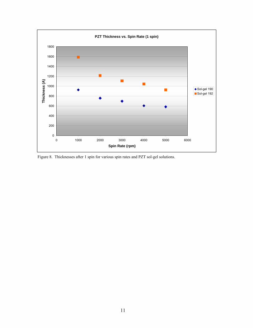
The first part of the spin rate test investigated the thickness of deposited PZT as a function of spin rate. The second part, investigating the dielectric and ferroelectric properties as a function of spin rate, was not completed, and will be left for future work. The results of the first part can be found in figures 9 and 10. Sol-gel solution 191 was to be tested, but yielded poor test samples because of excessive crystal formation, likely due to drying of the solution. New test samples will be prepared for spin rate testing of this solution during future experiments. Figure 8 shows the effects of differing solution molarity. Per spin, solution 192 deposits more PZT than solution 190, owing to its higher molarity. Figures 9 and 10 show all the thicknesses up to 4000 Å by spin for solution 190 and 192, respectively. The preliminary results of the spin rate test show that increasing the spin rate from 3000 to 5000 rpm is indeed a viable method of reducing device thickness. Whether acceptable performance is maintained depends on the dielectric and ferroelectric tests of the spin rate samples.
10
PZT Thickness vs. Spin Rate (1 spin)
0
200
400
600
800
1000
1200
1400
1600
1800
0 1000 2000 3000 4000 5000 6000
Spin Rate (rpm)
Thic
knes
s (A
)
Sol-gel 190Sol-gel 192
Figure 8. Thicknesses after 1 spin for various spin rates and PZT sol-gel solutions.
11

PZT Thickness vs. Spin Rate (Solution 190)
0
500
1000
1500
2000
2500
3000
3500
4000
4500
5000
0 1000 2000 3000 4000 5000 6000
Spin Rate (rpm)
Thic
knes
s (A
) 1 spin2 spins3 spins4 spins5 spins6 spins
Figure 9. Thicknesses by spin for sol-gel solution 190.
12

PZT Thickness vs. Spin Rate (Solution 192)
0
500
1000
1500
2000
2500
3000
3500
4000
4500
5000
0 1000 2000 3000 4000 5000 6000
Spin Rate (rpm)
Thic
knes
s (A
)
1 spin2 spins3 spins4 spins
Figure 10. Thicknesses by spin for sol-gel solution 192.
13
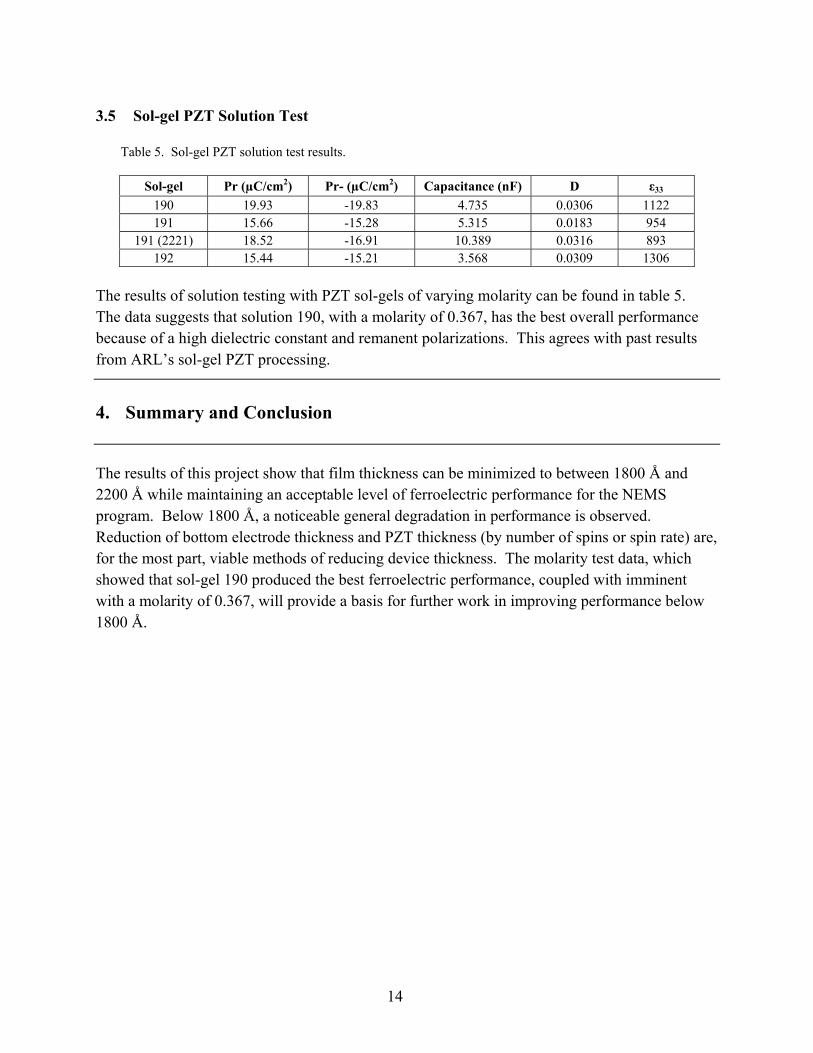
3.5 Sol-gel PZT Solution Test
Table 5. Sol-gel PZT solution test results.
Sol-gel Pr (µC/cm2) Pr- (µC/cm2) Capacitance (nF) D ε33 190 19.93 -19.83 4.735 0.0306 1122 191 15.66 -15.28 5.315 0.0183 954
191 (2221) 18.52 -16.91 10.389 0.0316 893 192 15.44 -15.21 3.568 0.0309 1306
The results of solution testing with PZT sol-gels of varying molarity can be found in table 5. The data suggests that solution 190, with a molarity of 0.367, has the best overall performance because of a high dielectric constant and remanent polarizations. This agrees with past results from ARL’s sol-gel PZT processing.
4. Summary and Conclusion
The results of this project show that film thickness can be minimized to between 1800 Å and 2200 Å while maintaining an acceptable level of ferroelectric performance for the NEMS program. Below 1800 Å, a noticeable general degradation in performance is observed. Reduction of bottom electrode thickness and PZT thickness (by number of spins or spin rate) are, for the most part, viable methods of reducing device thickness. The molarity test data, which showed that sol-gel 190 produced the best ferroelectric performance, coupled with imminent with a molarity of 0.367, will provide a basis for further work in improving performance below 1800 Å.
14

Symbols, Abbreviations, and Acronyms
Å Angstrom
ARL U.S. Army Research Laboratory
cm centimeter
CMOS complementary metal-oxide semiconductor
DARPA Defense Advanced Research Projects Agency
DC direct current
kHz kilohertz
Krpm kilo rotations per minute
min minute
mm millimeter
NEMS nanoelectromechanical system
Pt platinum
PZT lead zirconate titanate
rpm revolutions per minute
RTA rapid thermal anneal
s second
sccm standard cubic centimeters per minute
SiO2 silicon oxygen
Ti titanium
UV ultraviolet
μm micrometer
Zr zirconium
15

16
Distribution List
No. of Copies Organization
1 pdf ADMNSTR DEFNS TECHL INFO CTR DTIC OCP (ELECTRONIC COPY) 8725 JOHN J KINGMAN RD STE 0944 FT BELVOIR VA 22060-6218
5 HC US ARMY RSRCH LAB
IMNE ALC IMS MAIL & RECORDS MGMT AMSRD ARL D J M MILLER (1 COPY) AMSRD ARL CI OK TL TECHL LIB (2 COPIES) AMSRD ARL CI OK T TECHL PUB (2 COPIES) 2800 POWDER MILL ROAD ADELPHI MD 20783-1197
1 HC US ARMY RESEARCH LAB (1 COPY)
AMSRD CI OK TP TECHL LIB ATTN T LANDFRIED APG MD 21005
8 HC US ARMY RSRCH LAB AMSRD ARL SE RL R POLCAWICH (5 COPIES) AMSRD ARL SE RL V RAO (1 COPY) AMSRD ARL SE RL M DUBEY (1 COPY) AMSRD ARL SE RL R PIEKARZ (1 COPY) 2800 POWDER MILL ROAD BLDG 207 ADELPHI MD 20783-1197 Total: 15 (1 Electronic, 14 HCs)