Embed Size (px)
Citation preview
Regulation of PV Panel Voltage
using PI-P&O Control Algorithm
A thesis submitted in partial fulfilment of the requirements for the degree of
Master of Technology
in
Electrical Engineering (Specialization:Control & Automation)
by
Atanu Banerjee
Department of Electrical Engineering National Institute of Technology, Rourkela
May, 2014
Regulation of PV Panel Voltage
using PI-P&O Control Algorithm
A thesis submitted in partial fulfilment of the requirements for the degree of
Master of Technology
in
Electrical Engineering (Specialization:Control & Automation)
by
Atanu Banerjee
under the guidance of
Prof. Susovon Samanta
Department of Electrical Engineering National Institute of Technology, Rourkela
May, 2014

Department of Electrical EngineeringNational Institute of Technology, Rourkela
This is to certify that the project entitled, “
Control Algorithm” submitted by
an authentic work carried out by him under my supervision and guidance for the partial
fulfilment of the requirements for the award of
Engineering during the academic
Rourkela. The candidate has fulfilled all the prescribed requirements. The Thesis which is based
on candidate’s own work, has not been submitte
thesis is of standard requirement for the award of a Master of
Engineering.
Date: Place:
Department of Electrical Engineering National Institute of Technology, Rourkela
CERTIFICATE
is to certify that the project entitled, “Regulation of PV Panel Voltage using PI
” submitted by Atanu Banerjee in “Control & Automation
an authentic work carried out by him under my supervision and guidance for the partial
fulfilment of the requirements for the award of Master of Technology
the academic session 2013-14 at National Institute of Technology
The candidate has fulfilled all the prescribed requirements. The Thesis which is based
on candidate’s own work, has not been submitted elsewhere for any degree
thesis is of standard requirement for the award of a Master of Technology in Electrical
Dr. Susovon Dept. of Electrical Engineering
National Institute of Technology, Rourkela
of PV Panel Voltage using PI-P&O
Automation” specialization is
an authentic work carried out by him under my supervision and guidance for the partial
Master of Technology in Electrical
National Institute of Technology,
The candidate has fulfilled all the prescribed requirements. The Thesis which is based
d elsewhere for any degree. In my opinion, the
echnology in Electrical
. Susovon Samanta Dept. of Electrical Engineering

ACKNOWLEDGEMENT
Firstly, I am grateful to the Department of Electrical Engineering, for giving me the opportunity to carry out this project, which is an integral fragment of thecurriculum in M. Tech programme at the National Institute of Technology, Rourkela. I would like to express my heartfelt gratitude and regards to my project guide, Prof. Susovon Samanta, for being the corner stone of my project. It was his incessant motivation and guidance during periods of doubts and uncertainties that has helped me to carry on with this project. I would also like to thank Prof. A.K Panda, Head of the Department, Electrical Engineering, for his guidance and support. I would also like to acknowledge the effort given by my friend and colleague Murlidhar Killi. I would also like to thank a lot of other friendsfor giving a patient eartomyproblems.I am also obliged to the staff of ElectricalEngineering for aiding me during the course of our project. Finally, I would like to take the opportunity to thank my parents and my brother for their constant support and encouragement during my entire Post Graduate programme.
Atanu Banerjee
212EE3223

Dedicated to my Family

ABSTRACT
The growing demand for the renewable energy resources, especially the solar energy, has drawn the interest of the researchers. The need for extraction of maximum energy has called for innovation of newer techniques so that the PV panel can be efficiently operated at its peak power under partial shading and dynamic atmospheric conditions.
In this thesis, we have discussed the regulation of the output voltage of the PV array. We have observed the characteristics of the PV Panel under different temperatures and solar irradiations. Perturb and Observe Maximum power point tracking algorithm has been employed to operate the panel voltage at its MPP. Firstly, the panel peak voltage is obtained directly by varying the duty cycle of the converter. The direct duty Ratio control technique causes stress on the switch of the DC-DC converter besides loss of a significant amount of power. Therefore a PI controller has been implemented to regulate the panel voltage. A study using both DC-DC buck and boost converter as an interface between the PV Panel and the load has been presented. The PI controller prevents oscillation around the MPP apart from improving the steady state response and the settling time. A detailed analysis of the modeling of the PV array and DC-DC converters has been produced which helps in designing an efficient PI controller.
.

CONTENTS
List of Figures
List of Tables
Chapter 1 Introduction 1
1.1 Literature Review 2 1.2 Thesis Objective 3 1.3 Thesis Layout 4
Chapter 2 Analysis and Modeling of a PV based system 5
2.1 Introduction 5 2.2 PV Module Modeling 5 2.3 State Space Modeling Of Boost Converter 8
2.3.1 With Resistive Load 8 2.3.2 WithBattery Load 11
2.4 State Space Modeling Of Buck Converter 14 2.4.1 With Resistive Load 14 2.4.2 With Battery Load 18
Chapter 3 Maximum Power Point Tracking Algorithms 20
3.1 Introduction 21 3.2 Fractional Open Circuit Voltage 21 3.3 Fractional Short Circuit Current 22 3.4 Incremental Conductance Algorithm 22 3.5 Perturb and Observe Algorithm 23
Chapter 4 Perturb and Observe Algorithm 25
4.1 Introduction 25 4.2 Direct Duty Ratio Control . 27 4.3 PI Control 28
4.3.1 PI Tuning 29
Chapter 5 Results and Discussions 30 I Conclusion 39
II Future Work 39 III References 40
LIST OF FIGURES
Fig. No. Figure Description No. Page No.
Fig. 2.1 Non-linear I-V characteristics of the PV Module 6
Fig. 2.2 Equivalent circuit of a PV cell 6
Fig. 2.3 Linear equivalent circuit at the linearization point 7
Fig. 2.4
On-State circuit diagram of the Boost converter with resistive load
8
Fig. 2.5
Off-State circuit diagram of the Boost converter with resistive load
9
Fig. 2.6
On-State circuit diagram of the Boost converter with battery load
11
Fig. 2.7
Off-State circuit diagram of the Boost converter with battery load
13
Fig. 4.3
PV Module interfaced with a battery through a input regulated converter
28
Fig. 5.1 Power versus Voltage of a PV Module 30
Fig. 5.2 Current versus Voltage of a PV Module 30
Fig. 5.3 PV Power of a Buck converter using DDC 31
Fig. 5.4 PV Voltage versus time of a Buck converter using DDC 31
Fig. 5.5 PV Current of a Buck converter using DDC 32
Fig. 5.6 Duty Cycle of a Buck converter using DDC 32
Fig. 5.7 PV Power of a Buck converter using PI 33
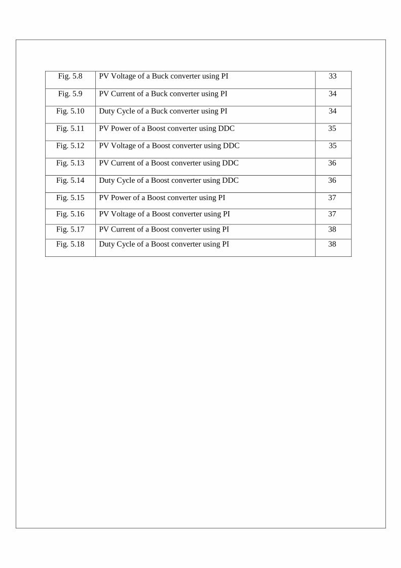
Fig. 5.8 PV Voltage of a Buck converter using PI 33
Fig. 5.9 PV Current of a Buck converter using PI 34
Fig. 5.10 Duty Cycle of a Buck converter using PI 34
Fig. 5.11 PV Power of a Boost converter using DDC 35
Fig. 5.12 PV Voltage of a Boost converter using DDC 35
Fig. 5.13 PV Current of a Boost converter using DDC 36
Fig. 5.14 Duty Cycle of a Boost converter using DDC 36
Fig. 5.15 PV Power of a Boost converter using PI 37
Fig. 5.16 PV Voltage of a Boost converter using PI 37
Fig. 5.17 PV Current of a Boost converter using PI 38
Fig. 5.18 Duty Cycle of a Boost converter using PI 38

LIST OF TABLES
Table No. Table Description Page No.
1. Parameters of the PV Module 7

1
CHAPTER 1
Introduction
With the reserve of fossil fuels diminishing and rise in the global temperature, the need to look for sustainable energy resources has become indispensable. The sustainable energy not only reduces the consumption of fossil fuels but also prevents the rising temperature of the earth besides diminishing the various pollutants emitted by it.
The main forms of renewable energy resources are Solar Energy, Wind Energy and Hydro Energy. The problem associated with hydro energy is that it is seasonal dependant where as the main factor that has caused researchers’ inclination for solar energy a little more than wind energy is that it is plentily available throughout the globe whereas establishing a wind farm is significantly costlier and depends on geographical locations. Moreover solar energy can be converted directly into electrical energy with the implementation of some power electronic devices.
Dynamic atmospheric conditions and partial shading reduces the efficiency of a PV Panel [11]. So a need for extracting maximum energy from the photovoltaic panel arises [2],[18]. This problem has been attended by the introduction of various MPPT methods. MPPT techniques helps in faster tracking and locking of photovoltaic panel MPP which increases its efficiency.
The growing research in this field has also reduced the cost of solar energy. Therefore Solar Energy has gained a lot of importance even in the rural areas.
1.1 Literature Review
Many Literatures are proposed on modeling of a Photovoltaic array.
M.G Villava et. al.[3] has modeled and simulated the PV array . The parameters of the non-linear I-V equation are found by adjusting the curve at open circuit, maximum power and short circuit points. Kun Ding et.al.[16] proposes a MATLAB-Simulink based PV module modeling which a controlled current source and an S-Function builder are used. The modeling in S-Function builder is done by some predigested functions. M.G Villava et. al.[5] proposes a study which dealt with regulation of the PV voltage. Regulation of
2
the converter input voltage improves the steady state response as well as stability of the closed loop system instead of regulating the bandwidth limited converter duty cycle, which makes it easier for the MPPT algorithm to work.
N.Femia et. al.[2] has proposed a method to avoid the negative behavior of the
P&O algorithm during rapidly changing environmental conditions by customizing the parameters of the P&O algorithm according to the dynamic behavior of a specific type of converter. Different methods of designing a PI controller was studied from Modern Control Engineering.
.
1.2 Thesis Objectives
• To study the solar cell model and observe its characteristics.
• State Space Modeling of DC-DC converters with a PV system. • To design and study the performance of a closed loop system with PI controller. • To study and implement Perturb and Observe algorithm in the
MATLAB-Simulink environment.
1.3 Thesis Layout
The first chapter gives a brief introduction about the need for solar energy. Then a literature review done in this context has also been produced. In the second chapter the state space modeling of DC-DC converters with a PV system has been done and a PV module was linearized about its MPP to find the transfer function between the control variable and the input voltage of the PV Module which is used to design a PI controller. In the third chapter, a comparative study of different MPP techniques is given. In the fourth chapter we have done a detailed study of the perturb and observe algorithm which has been used to simulation. The fifth chapter includes the results and conclusion.
3
CHAPTER 2
Analysis & Modeling of a PV based system
2.1 Introduction
The non-linear characteristics of the I-V curve of a PV panel can be divided into a current source region and a voltage source region. In this section we have linearized the PV panel at the MPP and a equivalent model of the PV panel is designed. The performance of a closed loop system can be improved by using a PI controller. The Parameters of a PI controller can be obtained by various methods like Frequency domain Analysis, Ziegler-Nichols criteria, Computational approach etc., for which modeling of a converter is essential. The aim of modeling a converter for controlling the voltage is to derive a Small-Signal transfer function that gives a relation between the small signal
voltage and the control variable .The negative sign indicates decrements in duty cycle causes increments in the input voltage [5]. The transfer function is then derived from the A, B, C and D matrices which is elaborated in the following section.
2.2 PV Module Modeling
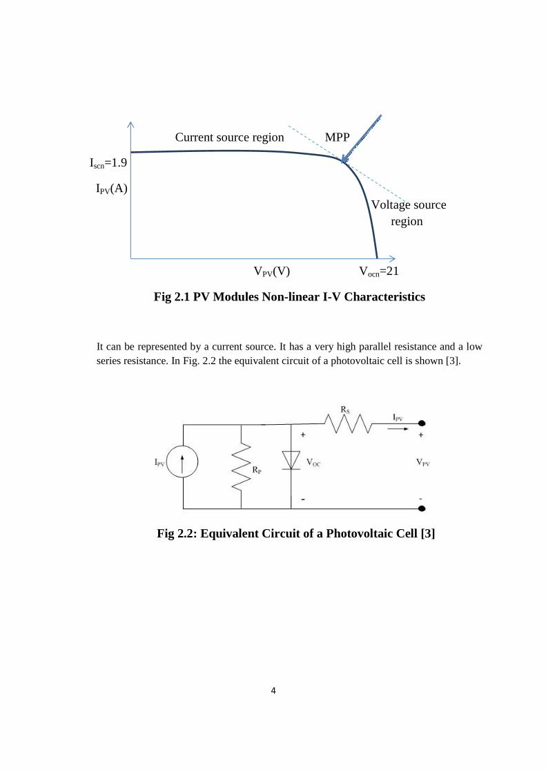
The non-linear I-V characteristics of a photovoltaic device is define in Fig 2.2.The I-V curve of the PV Module is shown in Fig. 2.1. I-V characteristics are defined as [3]
i I I e 1 !"! [3]
4
Current source region MPP
Iscn=1.9
IPV(A) Voltage source
region VPV(V) Vocn=21
Fig 2.1 PV Modules Non-linear I-V Characteristics
It can be represented by a current source. It has a very high parallel resistance and a low series resistance. In Fig. 2.2 the equivalent circuit of a photovoltaic cell is shown [3].
Fig 2.2: Equivalent Circuit of a Photovoltaic Cell [3]
5
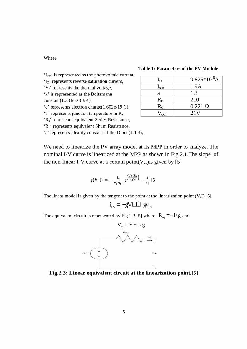
Where
Table 1: Parameters of the PV Module ‘I PV’ is represented as the photovoltaic current, ‘I O’ represents reverse saturation current, ‘V t’ represents the thermal voltage, ‘k’ is represented as the Boltzmann constant(1.381e-23 J/K), ‘q’ represents electron charge(1.602e-19 C), ‘T’ represents junction temperature in K, ‘Rs’ represents equivalent Series Resistance, ‘Rp’ represents equivalent Shunt Resistance, ‘a’ represents ideality constant of the Diode(1-1.3),
We need to linearize the PV array model at its MPP in order to analyze. The nominal I-V curve is linearized at the MPP as shown in Fig 2.1.The slope of the non-linear I-V curve at a certain point(V,I)is given by [5]
g$V, I' () *+, e-+.+ /
! [5]
The linear model is given by the tangent to the point at the linearization point (V,I) [5]
( )PV PVi gV I gv= − + +
The equivalent circuit is represented by Fig 2.3 [5] where eqR 1/g= − and
eqV V I / g= −
Fig.2.3: Linear equivalent circuit at the linearization point.[5]
IO 9.825*10-8A Iscn 1.9A a 1.3 RP 210 RS 0.221 Ω Vocn 21V
6
2.3 State Space Modeling of Boost Converter 2.3.1With Resistive Load
Fig 2.4: On-State Circuit diagram of Boost Converter with Resistive Load
ON STATE EQUATIONS
EQ C LI I I= + (1)
EQ PV CL
EQ
V V dVC I
R dt− = + (2)
PV C C CV V I R= + (3)
Putting equation (3) in (2) and simplifying, we get
( ) ( ) ( )L EQ EQC C
EQ C EQ C EQ C
I R VdV V
dt C R R C R R C R R= − − +
+ + + (4)
P V L L LV V I R 0− − = (5)

7
Putting equation (3) in (5) and solving
EQ C EQ CCLC L
EQ C EQ C EQ C
V R R RRdI 1V I
dt L(R R ) L L(R R ) L(R R )
= − − − + + +
(6)
C O OI I 0+ = (7)
( )CO CO COCOO
V I RdVC
dt R
+= − (8)
CO CO
O CO
dV V
dt C (R R )= −
+ (9)
EQ C L EQ C C EQPV
EQ C EQ C EQ C
V R I R R V RV
R R R R R R= − +
+ + + (10)
( )EQ C EQL C
EQ CEQ C EQ CLL
EQC C EQ
EQ C EQ C EQ CCO
CO
O CO
R R RR R0L L(R R )L R R L(R R )I
IR 1 1
V 0 V VC(R R ) C(R R ) C(R R )
VV 1 0
0 0C (R R )
− − ++ + = − − + + + + − +
ɺ
ɺ
ɺ
(11)
LEQ C EQ C
PV C EQEQ C EQ C EQ C
CO
IR R R R
V 0 V VR R R R R R
V
= − + + + +
(12)

8
Fig 2.5: Off-State Circuit diagram of Boost Converter with resistive Load
OFF STATE EQUATIONS
EQ C LI I I= + (13)
EQ PV CL
EQ
V V dVC I
R dt
−= + (14)
PV C C CV V I R= + (15) Putting equation (14) in (13) and solving, we get
C D
CE
(F!GH
I(!GH !D) D
IJ!GH !DKL
GH
IJ!GH !DK (16)
L C O OI I I= + (17)
CO CO COL CO
V I RI I
R
+= + (18)
COL CO CO CO
dVI R I R V C R
dt= + + (19)
Simplifying equation (18), we get

9
CO COL
O CO O CO
dV VI R
dt C (R R ) C (R R )= −
+ + (20)
P V L L L C O C O C OV V I R V I R 0− − − − = (21)
We know,
EQ C L EQC
EQ C
V V I RI
R R
− −=
+ (22)
L COCO
CO
I R VI
R R
−=+
(23)
Replacing equation (21)& (22) in equation (20),we get
C EQ EQ C EQ CCO COL LL
EQ C EQ C CO CO EQ C
V R R R V RR R V RdI IR
dt L(R R ) L R R R R L(R R ) L(R R )
= − + + − + + + + + +
(24)
( ) ( )
( ) ( )
( ) ( )
EQ C EQCO CL
EQ C CO COEQ C EQ CLL
EQC C EQ
EQ CEQ C EQ CCO
CO
O CO O CO
R R RR R1 R RRL R R R R L R RL R R L(R R )I
IR 1 1
V 0 V VC(R R )C R R C R R
VV 0R 1
0C R R C R R
− + + − + + ++ + = − − + ++ + − + +
ɺ
ɺ
ɺ
(25)
LEQ C EQ C
PV C EQEQ C EQ C EQ C
CO
IR R R R
V 0 V VR R R R R R
V
= − + + + +
(26)
[ ] 1pvvd
VG Y C SI A E
d
−= = = −
ɵ
ɵ
When RL=RC=RCO=0
GC DN
C
ON
C X(S' QSI ARS/E

10
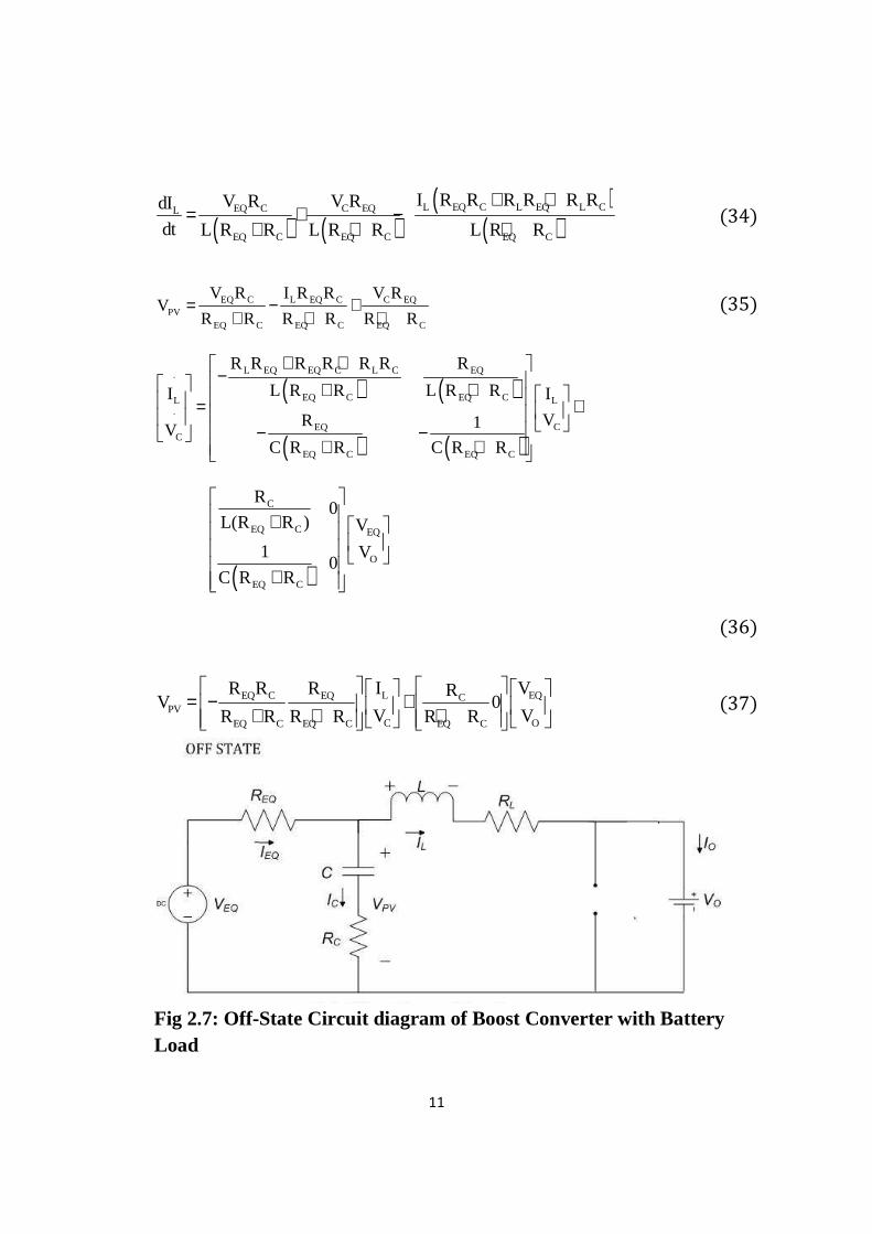
2.3.2 With Battery Load
Fig.2.6: On-State Circuit diagram of Boost Converter with Battery Load
ON STATE EQUATIONS ITU II L IV (27)
EQ PVC L
EQ
V VI I
R
−= + (28)
EQ C C C C EQ L EQV V I R I R I R− − = + (29)
EQ L EQC
CEQ C EQ C EQ C
V I RVI
R R R R R R= − −
+ + + (30)
( ) ( )EQ L EQC C
EQ C EQ C EQ C
V I RdV V
dt C(R R ) C R R C R R= − −
+ + + (31)
P V L L LV V I R 0− − = (32)
EQ L EQC
C C L L LEQ C EQ C EQ C
V I RVV R I R V 0
R R R R R R
+ − − − − = + + +
(33)
11
( ) ( )( )
( )L EQ C L EQ L CEQ C C EQL
EQ C EQ C EQ C
I R R R R R RV R V RdI
dt L R R L R R L R R
+ += + −
+ + + (34)
EQ C L EQ C C EQ
PVEQ C EQ C EQ C
V R I R R V RV
R R R R R R= − +
+ + + (35)
( ) ( )
( ) ( )
L EQ EQ C L C EQ
EQ C EQ CL L
CEQC
EQ C EQ C
R R R R R R R
L R R L R RI I
VR 1VC R R C R R
+ + − + + = + − −
+ +
ɺ
ɺ
( )
C
EQ C EQ
O
EQ C
R0
L(R R ) V
1 V0
C R R
+
+
(36)
L EQEQ C EQ CPV
C OEQ C EQ C EQ C
I VR R R RV 0
V VR R R R R R
= − + + + +
(37)
Fig 2.7: Off-State Circuit diagram of Boost Converter with Battery Load

12
OFF-STATE EQUATIONS
EQ C LI I I= + (38)
EQ PVC L
EQ
V VI I
R
−= + (39)
EQ C C C C EQ L EQV V I R I R I R− − = + (40)
EQ L EQCC
EQ C EQ C EQ C
V I RVI
R R R R R R= − −
+ + + (41)
( ) ( )EQ L EQC C
EQ C EQ C EQ C
V I RdV V
dt C(R R ) C R R C R R= − −
+ + + (42)
C C C L L L OV I R V I R V 0+ − − − = (43)
( )( )
L EQ C L EQ L CEQ C C EQ OL
EQ C EQ C EQ C
I R R R R R RV R V R VdI
dt L(R R ) L(R R ) LL R R
+ += + − −
+ + + (44)
( ) ( )
( ) ( )
L EQ EQ C L C EQ
EQ C EQ CL L
CEQC
EQ C EQ C
R R R R R R R
L R R L R RI I
VR 1VC R R C R R
+ + − + + = + − −
+ +
ɺ
ɺ
( )
( )
C
EQ C EQ
O
EQ C
R 1
LL R R V
V10
C R R
− +
+
(45)
L EQEQ C EQ CPV
C OEQ C EQ C EQ C
I VR R R RV 0
V VR R R R R R
= − + + + +
(46)
GC
C CQSI ARS/E

13
When RL=RC=RCO=0
GC
C D
C X(s) QSI ARS/E
2.4 State Space Modeling of Buck Converter 2.4.1 With Resistive Load
Fig 2.8: On-State Circuit diagram of Buck Converter with Resistive Load
ON STATE EQUATIONS PV EQ
C LEQ
V VI I 0
R
−+ + = $47'
PV C C CV R I V= + $48' Putting equation $48' in $47' and simplifying, we get
EQ L EQC C
EQ C EQ C EQ C
V I RdV V
dt C(R R ) C(R R ) C(R R )= − −
+ + + $49'
OL CO
VI I
R= + $50'
14
CO CO CO COL O
dV I R VI C
dt R
+= + (51)
( )CO COL
O CO O CO
dV VI R
dt C (R R) C R R= −
+ + (52)
P V L L L C O C O C OV I R V I R V 0− − − − = (53)
CO LC C C L L CO O CO
dV dII R V I R R C V L
dt dt+ − − − = (54)
Putting equation (52) in (54) and Simplifying, we get
( ) ( ) ( )EQ C C C CO COL
COEQ C EQ C
V R V R V RdI1 1
dt L L L R RL R R L R R
= + − − − ++ +
(55)
( ) ( ) ( ) ( )
( ) ( )
( ) ( )
EQ CCO C COL
COEQ C EQ C EQ CL
LEQ
C CEQ C EQ C
COCO
O CO O CO
R RR R R RR 1 1
L L L R R LL R R L R R L R RII
R 1V 0 V
C R R C R RV
V R 10
C R R C R R
− − − − − ++ + + = − − + + − + +
ɺ
ɺ
ɺ
( )
( )
C
EQ C
EQ
EQ C
R
L R R
1V
C R R
0
+
+ +
(56)
EQ C C EQ L EQ CPV
EQ C EQ C EQ C
V R V R I R RV
R R R R R R= + −
+ + + (57)
LEQ C EQ C
PV C EQEQ C EQ C EQ C
CO
IR R R R
V 0 V VR R R R R R
V
= − + + + +
(58)

15
Fig 2.9: Off-State Circuit diagram of Buck Converter with Resistive Load
OFF-STATE EQUATIONS
EQ PVC
EQ
V VI
R
−= (59)
( )EQ C
CEQ C EQ C
V VI
R R R R= −
+ + (60)
( ) ( )EQC C
EQ C EQ C
VdV V
dt C R R C R R= −
+ +
(61)
OL CO
VI I
R= + (62)
CO CO COL CO
I R VI I
R
+= + (63)
( ) ( )CO COL
O CO O CO
dV VI R
dt C R R C R R= −
+ + (64)
L L L C O C O C OI R V I R V 0− − − − = (65)

16
CO LL L O CO CO
dV dII R C R V L
dt dt− − − = (66)
Putting equation (63) in (65), we get
( ) ( )COL L
L COCO CO
RRdI R RI V
dt L L R R L R R
= − − + − + +
(67)
( ) ( )
( )
( ) ( )
( )
COL
CO COLL
C C EQEQ C EQ C
COCO
O CO O CO
R RR R0
L L R R L R R 0II
1 1V 0 0 V V
C R R C R RV
V R 1 00
C R R C R R
− − − + + = − + + + − + +
ɺ
ɺ
ɺ
(68)
EQ C C EQPV
EQ C EQ C
V R V RV
R R R R= +
+ + (69)
LEQ C
PV C EQEQ C EQ C
CO
IR R
V 0 0 V VR R R R
V
= + + +
(70)
GC Z
C CQSI ARS/E
When RV RI RI 0
GC ONC DN
C QSI ARS/E
17
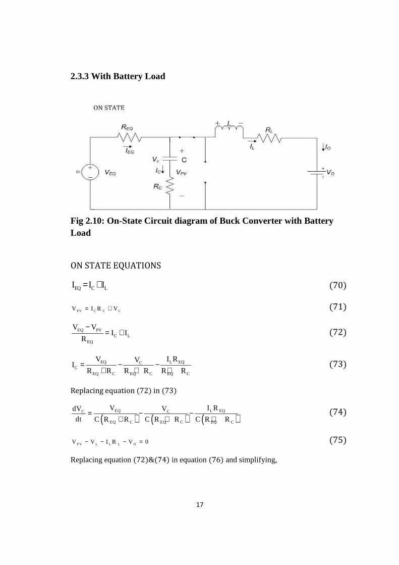
2.3.3 With Battery Load
Fig 2.10: On-State Circuit diagram of Buck Converter with Battery Load
ON STATE EQUATIONS
EQ C LI I I= + (70)
PV C C CV I R V= + (71)
EQ PVC L
EQ
V VI I
R
−= + (72)
EQ L EQCC
EQ C EQ C EQ C
V I RVI
R R R R R R= − −
+ + + (73)
Replacing equation (72) in (73)
( ) ( ) ( )EQ L EQC C
EQ C EQ C EQ C
V I RdV V
dt C R R C R R C R R= − −
+ + + (74)
P V L L L OV V I R V 0− − − = (75)
Replacing equation (72)&(74) in equation (76) and simplifying,
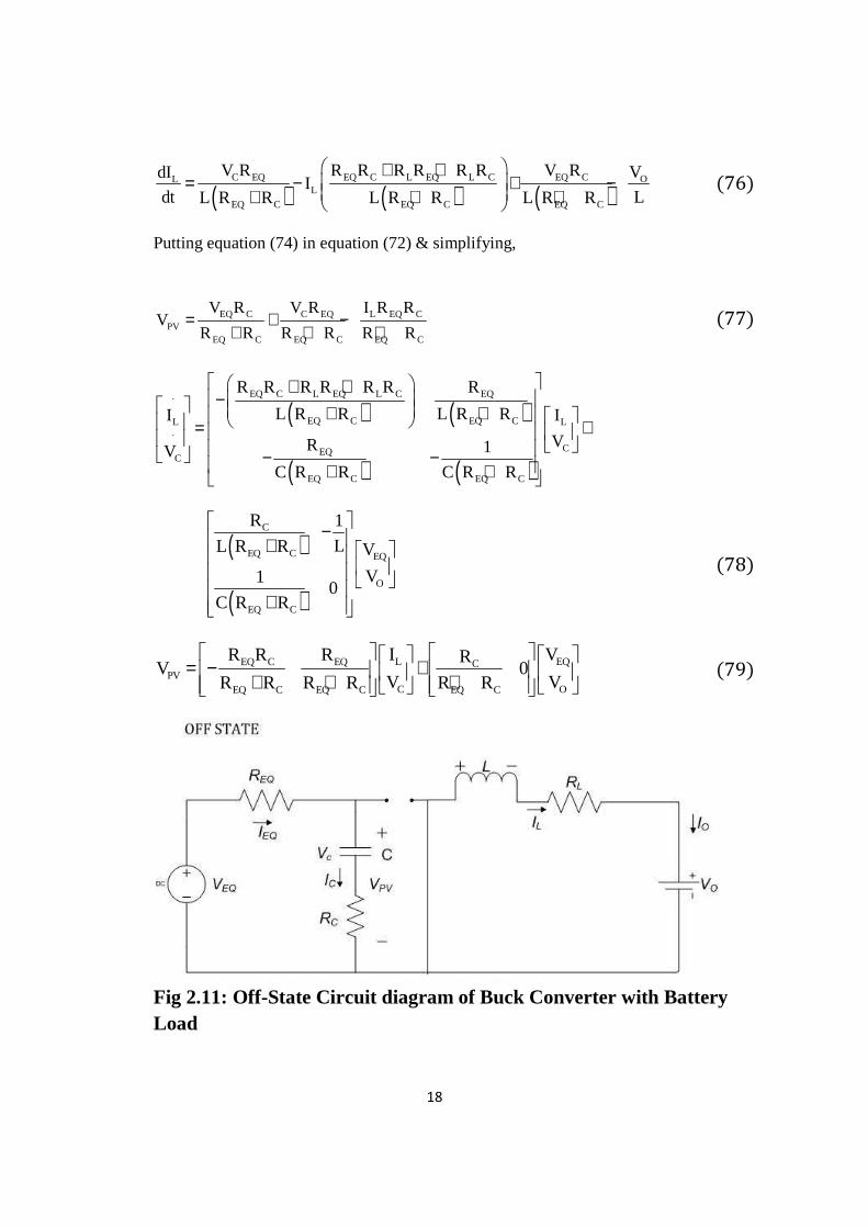
18
( ) ( ) ( )C EQ EQ C L EQ L C EQ C OL
L
EQ C EQ C EQ C
V R R R R R R R V R VdII
dt LL R R L R R L R R
+ += − + −
+ + + (76)
Putting equation (74) in equation (72) & simplifying,
EQ C C EQ L EQ CPV
EQ C EQ C EQ C
V R V R I R RV
R R R R R R= + −
+ + + (77)
( ) ( )
( ) ( )
EQ C L EQ L C EQ
EQ C EQ CL L
CEQC
EQ C EQ C
R R R R R R R
L R R L R RI I
VR 1VC R R C R R
+ + − + + = + − − + +
ɺ
ɺ
( )
( )
C
EQ C EQ
O
EQ C
R 1
LL R R V
V10
C R R
− +
+
(78)
L EQEQ C EQ CPV
C OEQ C EQ C EQ C
I VR R R RV 0
V VR R R R R R
= − + + + +
(79)
Fig 2.11: Off-State Circuit diagram of Buck Converter with Battery Load
19
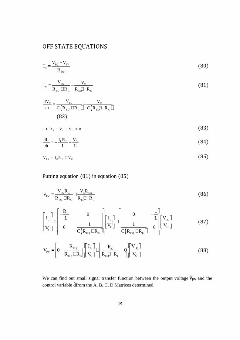
OFF STATE EQUATIONS
EQ PVC
EQ
V VI
R
−= (80)
EQ CC
EQ C EQ C
V VI
R R R R= −
+ + (81)
( ) ( )EQC C
EQ C EQ C
VdV V
dt C R R C R R= −
+ +
(82)
L L L OI R V V 0− − − = (83)
OL L L VdI I R
dt L L= − − (84)
PV C C CV I R V= + (85)
Putting equation (81) in equation (85)
EQ C C EQPV
EQ C EQ C
V R V RV
R R R R= +
+ + (86)
( ) ( )
L
L L EQ
C OC
EQ CEQ C
R 100
I I VLL11 V V00V
C R RC R R
−− = + − ++
ɺ
ɺ (87)
L EQEQ CPV
C OEQ C EQ C
I VR RV 0 0
V VR R R R
= + + +
(88)
We can find out small signal transfer function between the output voltage V and the
control variable dfrom the A, B, C, D Matrices determined.
20
CHAPTER 3
Maximum Power Point Tracking Algorithms
3.1 Introduction
When we install a solar panel or a array of solar panels without a MPPT technique, it often leads to wastage of power, which ultimately requires more number of panels for the same amount of power requirement. Also whenever a battery is connected directly to the panel, it results in premature failure of battery or loss capacity owing to lack of a proper end-of-charge process and higher voltage. So, absence of a MPPT method results in higher cost. The main aim of a MPPT technique is to automatically find the operating voltage of the panel that delivers maximum power to the load. When a single MPPT is connected to large number of panels, it will yield a good result but in case of partial shading, the combined power output curve will have multiple maximas which might confuse the algorithm.
3.2 Fractional Open Circuit Voltage
A linear relation with the open circuit voltage is maintained by the maximum power point voltage under different temperature and irradiance conditions.
Vf K VI
Constant KV is always dependable on the type and configuration of the Solar Panel. The open circuit voltage. For FOCV the open circuit voltage of the panel has to be measured first in order to determine the MPP voltage. One way of doing it is the system periodically disconnects the system from the load to measure the open circuit voltage and calculate the MPP. Clearly this procedure leads to wastage of power. Another method could be by using one or more monitoring cells but they must also be chosen and placed very carefully to measure the correct open circuit voltage. Even though the method is simple and robust, we can only make a crude approximation of the MPP. The value of KV has been experimentally found out to be between 0.7-0.8
21
3.3Fractional Short Circuit Current
The MPP can also be calculated from the short circuit current of the panel because IMPP is linearly dependent on the short circuit current under varying atmospheric conditions.
If K(IhI
Measuring ISC is more difficult as compared to VOC, since it not only leads to power
losses and heat dissipation, it requires additional switches and current sensors which increases the cost of installation. The value of KI is nominally considered between 0.79-0.91.
3.4 Incremental Conductance
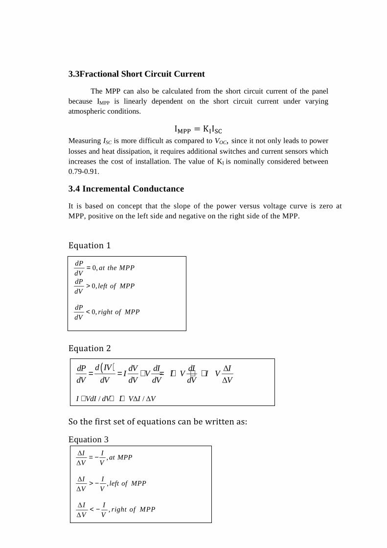
It is based on concept that the slope of the power versus voltage curve is zero at MPP, positive on the left side and negative on the right side of the MPP.
Equation 1
Equation 2
So the first set of equations can be written as: Equation 3
0, dP
at the MPPdV
=
0, dP
left of MPPdV
>
0, dP
right of MPPdV
<
( ) ∆
∆
d IVdP dV dI dI II V I V I V
dV dV dV dV dV V= = + = + ≅ +
/ ∆ /∆I VdI dV I V I V+ ≅ +
∆,
∆
I Iat MPP
V V= −
∆,
∆
I Ileft of MPP
V V> −
∆,
∆
I Iright of MPP
V V< −

22
The concept behind this is to make a comparison between the incremental conductance to the instantaneous conductance. It is operated by this logic until the MPP is reached by increasing or decreasing voltage.
3.5 Perturb and Observe
Perturb & Observe is generally used algorithms for its simplicity of implementation. The algorithm introduces a perturbation in the module voltage. The module voltage is modified by updating the converter duty cycle.

23
CHAPTER 4
Perturb & Observe Algorithm
4.1 Introduction
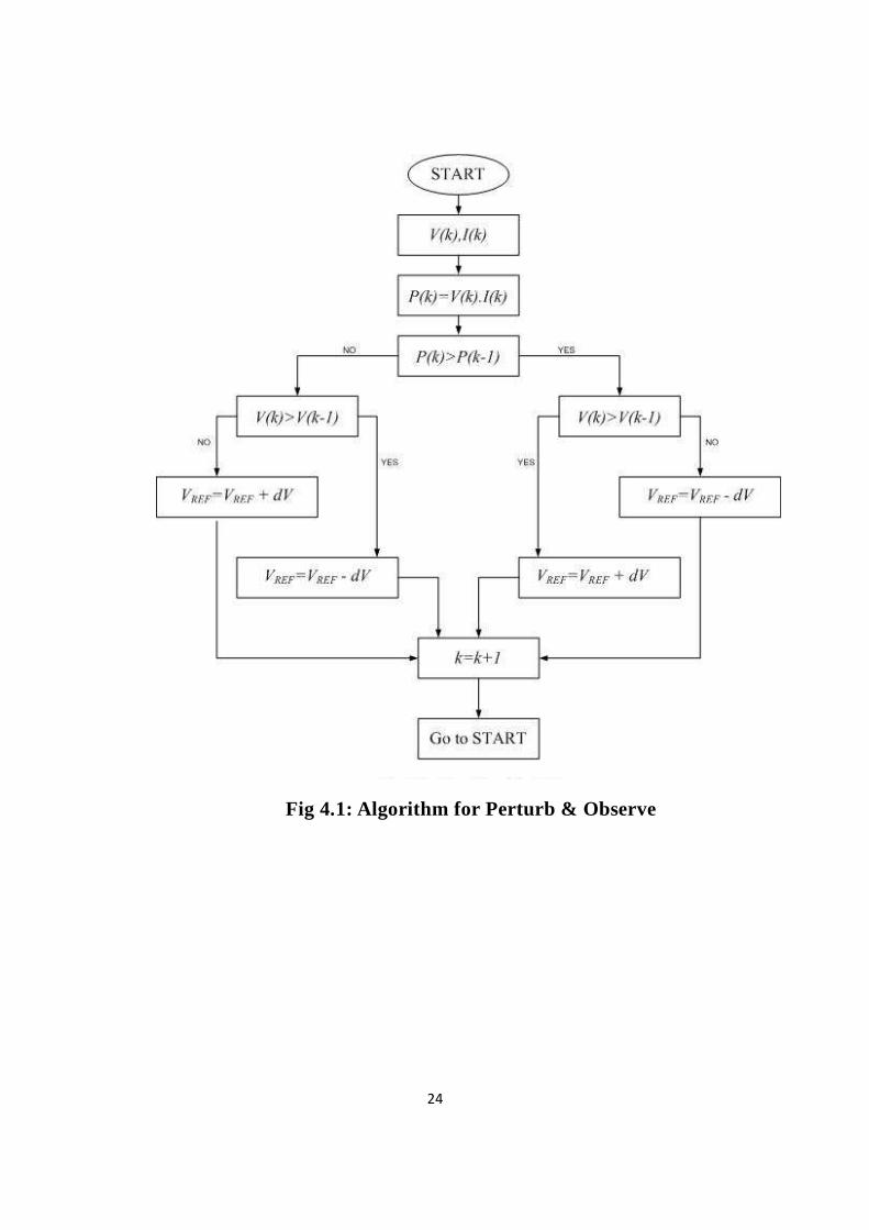
When an increment is made in the Module voltage, the algorithm checks the present power reading and the previous one. If the power has increased it keeps increasing the voltage or it reverses the direction. This process is continued at each step until the peak power is reached. After reaching there, the algorithm oscillates about the MPP.
The basic algorithm is based on using a fixed step to increase or decrease the operating voltage. The deviation while oscillating around the MPP is dependent on step size chosen. Choosing a small step size reduces the oscillation around the MPP but increases tracking time adversely, while a bigger step size reduces the tracking time but increases power loss due to the oscillation. The algorithm for perturb and observe is shown in Fig. 4.1.
The Perturb and Observe algorithm can be validated either directly by operating the converter’s duty cycle or by generating a reference voltage or current signal which is tracked by a PI controller. The output of the PI controller is then compared with a reference constant value to generate the PWM signal. The different control loops are elaborated in the following section.
24
Fig 4.1: Algorithm for Perturb & Observe
25
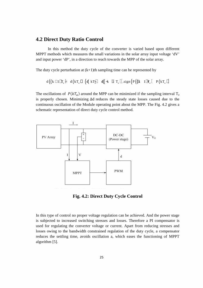
4.2 Direct Duty Ratio Control
In this method the duty cycle of the converter is varied based upon different MPPT methods which measures the small variations in the solar array input voltage ‘dV’ and input power ‘dP’, in a direction to reach towards the MPP of the solar array. The duty cycle perturbation at (k+1)th sampling time can be represented by
( )( ) ( ) ( ) ( )( )( ) ( )( ) ( )( )a a a a a ad k 1 T d kT d kT d k 1 T .sign P k 1 P T kT+ = + − − + −
The oscillations of i(jkl) around the MPP can be minimized if the sampling interval Ta is properly chosen. Minimizing ∆d reduces the steady state losses caused due to the continuous oscillation of the Module operating point about the MPP. The Fig. 4.2 gives a schematic representation of direct duty cycle control method.
Fig. 4.2: Direct Duty Cycle Control
In this type of control no proper voltage regulation can be achieved. And the power stage is subjected to increased switching stresses and losses. Therefore a PI compensator is used for regulating the converter voltage or current. Apart from reducing stresses and losses owing to the bandwidth constrained regulation of the duty cycle, a compensator reduces the settling time, avoids oscillation a, which eases the functioning of MPPT algorithm [5].
26
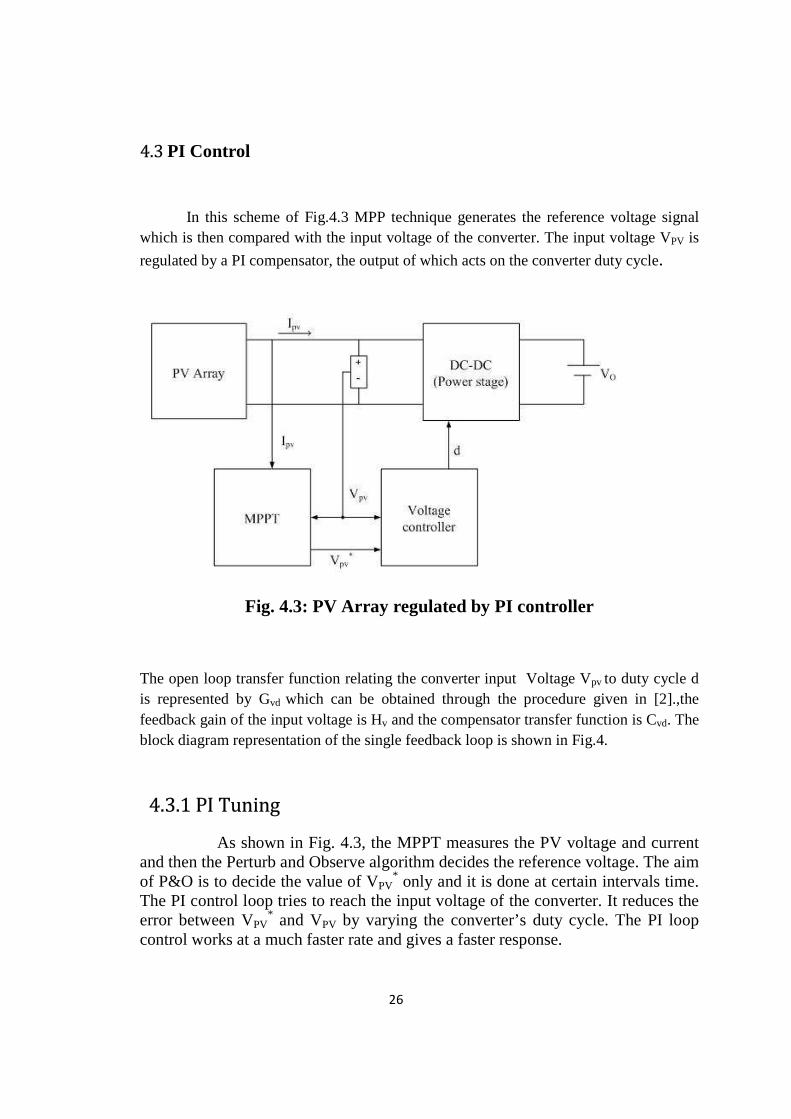
4.3 PI Control
In this scheme of Fig.4.3 MPP technique generates the reference voltage signal which is then compared with the input voltage of the converter. The input voltage VPV is
regulated by a PI compensator, the output of which acts on the converter duty cycle.
Fig. 4.3: PV Array regulated by PI controller
The open loop transfer function relating the converter input Voltage Vpv to duty cycle d is represented by Gvd which can be obtained through the procedure given in [2].,the feedback gain of the input voltage is Hv and the compensator transfer function is Cvd. The block diagram representation of the single feedback loop is shown in Fig.4.
4.3.1 PI Tuning
As shown in Fig. 4.3, the MPPT measures the PV voltage and current and then the Perturb and Observe algorithm decides the reference voltage. The aim of P&O is to decide the value of VPV
* only and it is done at certain intervals time. The PI control loop tries to reach the input voltage of the converter. It reduces the error between VPV
* and VPV by varying the converter’s duty cycle. The PI loop control works at a much faster rate and gives a faster response.

27
CHAPTER 5
Results
The PV Module has been interfaced to a load resistance through DC-DC converters. The simulation results have been obtained for both Boost and Buck converters. The PV module characteristic has been shown under different irradiations. Secondly, Power and voltage curves have been obtained under two different irradiations using the direct duty ratio control technique. Lastly we have shown the input regulated power and voltage curves of the PV Module with both Buck and Boost converters using PI controller.
Fig. 5.1 Power versus Voltage of a PV Module
Fig. 5.2: Current versus Voltage of a PV Module
0 5 10 15 200
0.2
0.4
0.6
0.8
1
1.2
1.4PV Current vs PV Voltage
PV Voltage(V)
PV
Cur
rent
(A)
600 W/m2
400 W/m2
Vm=16.23Im=1.02
Vm=15.78Im=0.6622
0 5 10 15 200
5
10
15
20
PV Voltage(V)
PV
Pow
er(W
)
PV Power vs PV Voltgae
400 W/m2
600 W/m2
Pm=16.68Vm=16.23
Pm=10.45Vm=15.78

28
5.1 Buck Converter 5.1.1 Direct Duty Ratio Control
Fig.5.3: PV Power of a Buck converter using DDC.
Fig.5.4: PV Voltage of a Buck converter using DDC.
0 0.2 0.4 0.6 0.8 1 1.2 1.4 1.6 1.8 20
5
10
15
20
time(s)
PV
Pow
er(W
)
PV Power vs time
g=400 w/m2
g=600w/m2
0 0.2 0.4 0.6 0.8 1 1.2 1.4 1.6 1.8 20
5
10
15
20
time(s)
PV
Vol
tage
(V)
PV Voltage vs time
g=600w/m2g=400w/m2

29
Fig. 5.5: PV Current of a Buck converter using DDC.
Fig. 5.6: Duty cycle of a Buck converter using DDC.
0 0.2 0.4 0.6 0.8 1 1.2 1.4 1.6 1.8 20.4
0.6
0.8
1
1.2
1.4
time(s)
PV
Cur
rent
(A)
PV Current vs time
G=400 W/m2
G=600 W/m2
0 0.2 0.4 0.6 0.8 1 1.2 1.4 1.6 1.8 20.4
0.5
0.6
0.7
0.8
time(s)
Dut
y C
ycle
Duty Cycle vs time
g=400 w/m2
g=600 w/m2
30
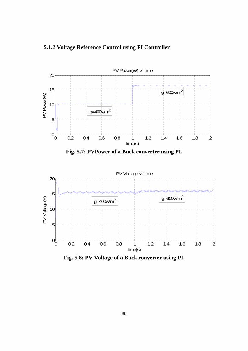
5.1.2 Voltage Reference Control using PI Controller
Fig. 5.7: PVPower of a Buck converter using PI.
Fig. 5.8: PV Voltage of a Buck converter using PI.
0 0.2 0.4 0.6 0.8 1 1.2 1.4 1.6 1.8 20
5
10
15
20
time(s)
PV
Pow
er(W
)
PV Power(W) vs time
g=600w/m2
g=400w/m2
0 0.2 0.4 0.6 0.8 1 1.2 1.4 1.6 1.8 20
5
10
15
20
time(s)
PV
Vol
tage
(V)
PV Voltage vs time
g=400w/m2 g=600w/m2

31
Fig. 5.9: PV Current of a Buck converter using PI.
Fig. 5.10: Duty Cycle of a Buck converter using PI.
0 0.2 0.4 0.6 0.8 1 1.2 1.4 1.6 1.8 20
0.5
1
1.5
time(s)
PV
Cur
rent
(A)
PV Current vs time
g=400w/m2
g=600w/m2
0 0.2 0.4 0.6 0.8 1 1.2 1.4 1.6 1.8 20.2
0.4
0.6
0.8
1
time(s)
Dut
y C
ycle
Duty Cycle vs time
g=400 /m2
g=600 /m2
32
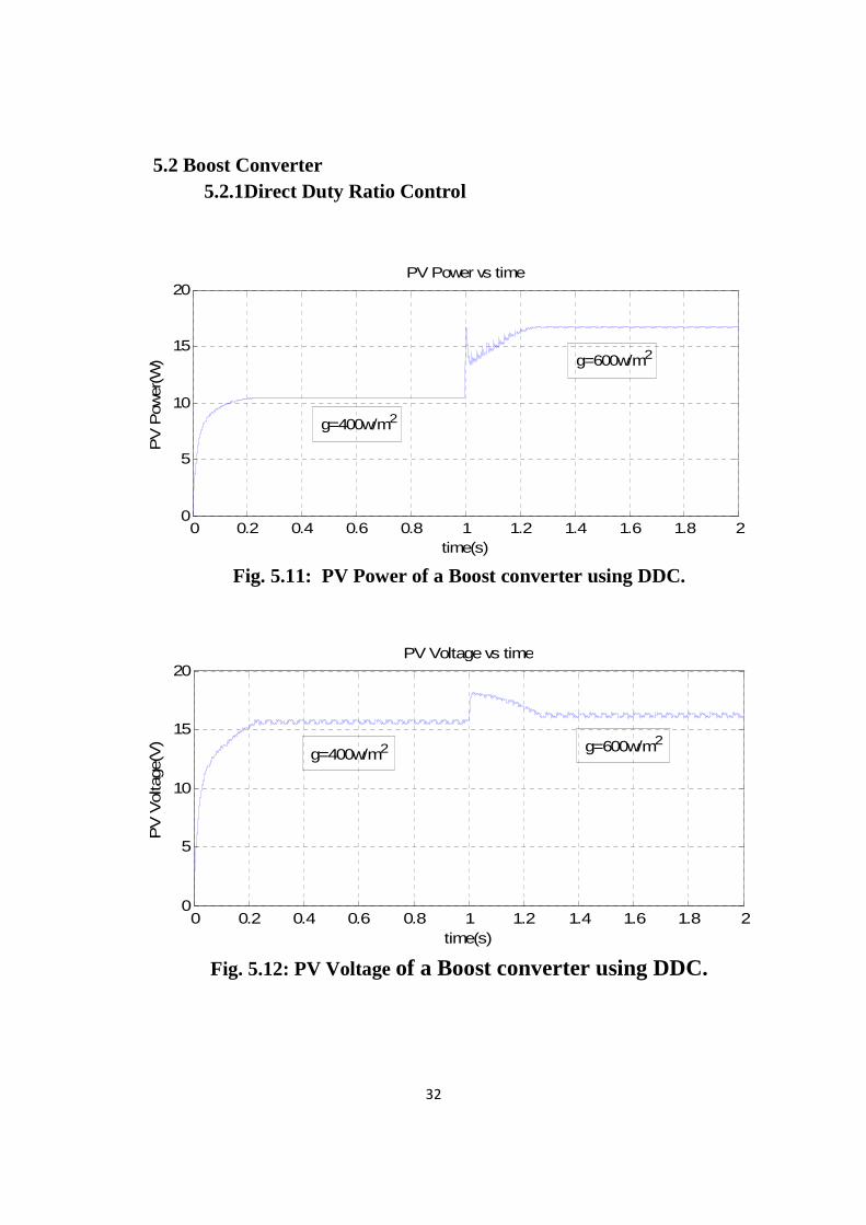
5.2 Boost Converter 5.2.1Direct Duty Ratio Control
Fig. 5.11: PV Power of a Boost converter using DDC.
Fig. 5.12: PV Voltage of a Boost converter using DDC.
0 0.2 0.4 0.6 0.8 1 1.2 1.4 1.6 1.8 20
5
10
15
20
time(s)
PV
Pow
er(W
)
PV Power vs time
g=400w/m2
g=600w/m2
0 0.2 0.4 0.6 0.8 1 1.2 1.4 1.6 1.8 20
5
10
15
20
time(s)
PV
Vol
tage
(V)
PV Voltage vs time
g=400w/m2 g=600w/m2
33
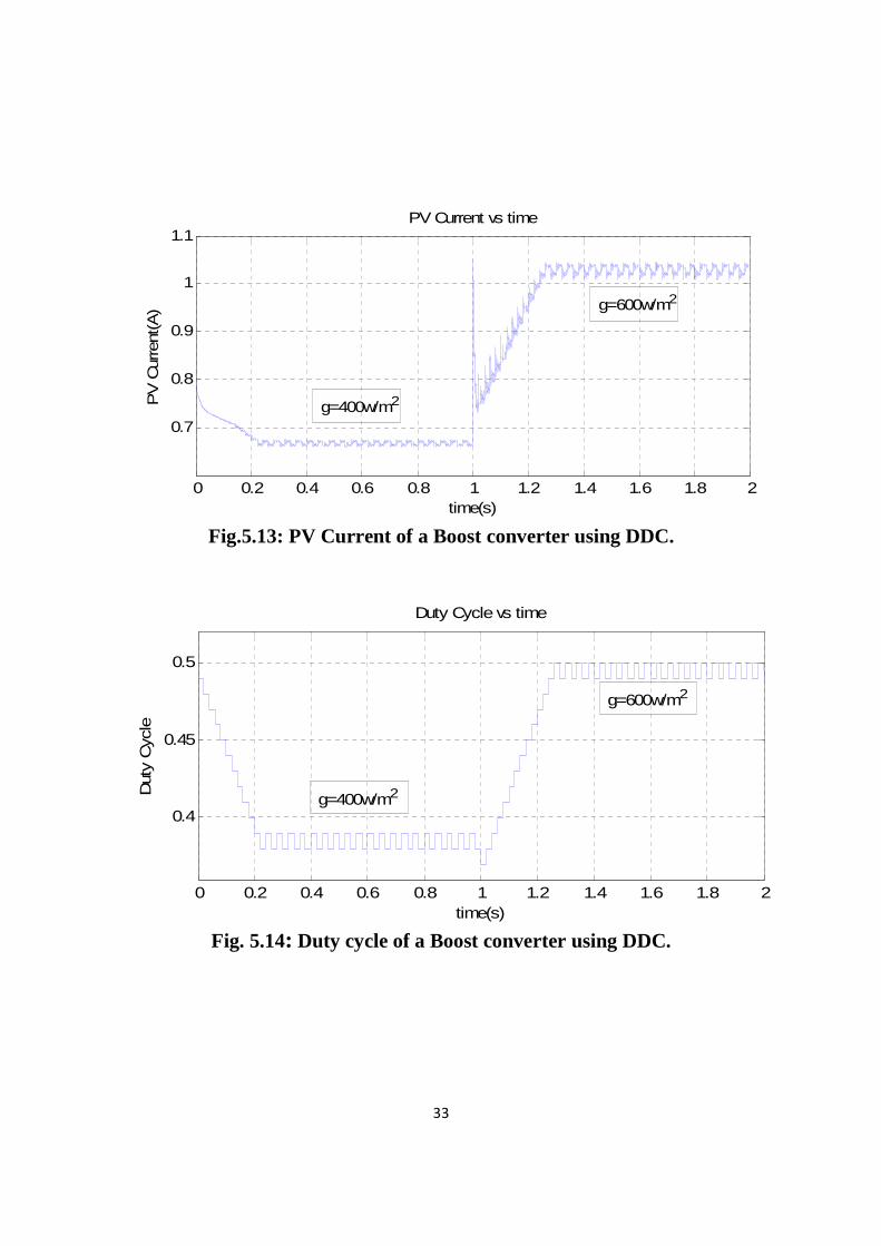
Fig.5.13: PV Current of a Boost converter using DDC.
Fig. 5.14: Duty cycle of a Boost converter using DDC.
0 0.2 0.4 0.6 0.8 1 1.2 1.4 1.6 1.8 2
0.7
0.8
0.9
1
1.1
time(s)
PV
Cur
rent
(A)
PV Current vs time
g=400w/m2
g=600w/m2
0 0.2 0.4 0.6 0.8 1 1.2 1.4 1.6 1.8 2
0.4
0.45
0.5
time(s)
Dut
y C
ycle
Duty Cycle vs time
g=600w/m2
g=400w/m2
34
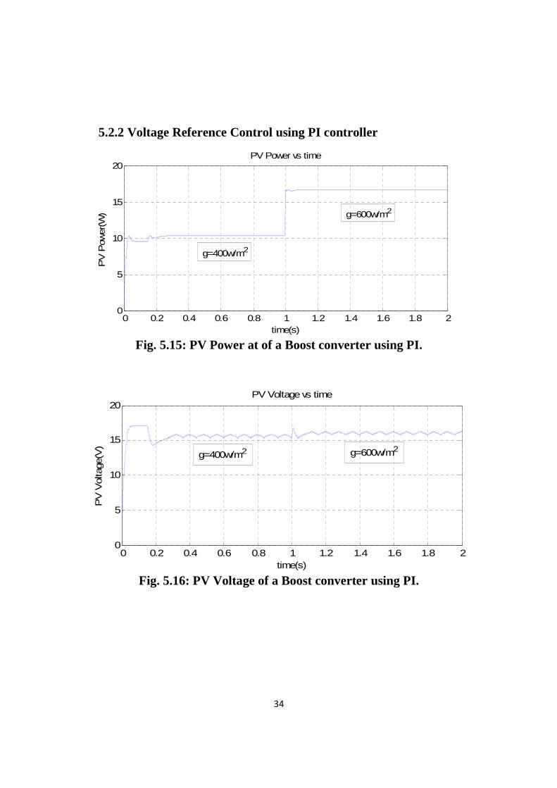
5.2.2 Voltage Reference Control using PI controller
Fig. 5.15: PV Power at of a Boost converter using PI.
Fig. 5.16: PV Voltage of a Boost converter using PI.
0 0.2 0.4 0.6 0.8 1 1.2 1.4 1.6 1.8 20
5
10
15
20
time(s)
PV
Pow
er(W
)
PV Power vs time
g=400w/m2
g=600w/m2
0 0.2 0.4 0.6 0.8 1 1.2 1.4 1.6 1.8 20
5
10
15
20
time(s)
PV
Vol
tage
(V)
PV Voltage vs time
g=600w/m2g=400w/m2
35
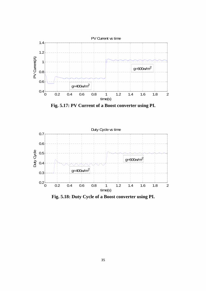
Fig. 5.17: PV Current of a Boost converter using PI.
Fig. 5.18: Duty Cycle of a Boost converter using PI.
0 0.2 0.4 0.6 0.8 1 1.2 1.4 1.6 1.8 20.4
0.6
0.8
1
1.2
1.4
time(s)
PV
Cur
rent
(A)
PV Current vs time
g=400w/m2
g=600w/m2
0 0.2 0.4 0.6 0.8 1 1.2 1.4 1.6 1.8 20.2
0.3
0.4
0.5
0.6
0.7
time(s)
Dut
y C
ycle
Duty Cycle vs time
g=400w/m2
g=600w/m2
36
I. Conclusion
The results were obtained in the MATLAB-Simulink environment. From the curves obtained both in the direct duty ratio control and the voltage reference control in which a PI controller is used to regulate the voltage of the PV array, it is evident that a PI controller helps in achieving a faster steady state response and avoids oscillations and overshoot as compared to direct duty ratio control.
A detailed study of the perturb and observe technique was done. We have also made a comparative analysis of the different MPPT techniques which guides us to choose the best among the available techniques in a particular environmental condition.
II. Future Work
• Implementation of global MPPT in case of partial shading phenomenon. • Avoiding drift phenomenon in P&O due to change in insolation level.
III. References
[1]W. Xiao, W.G. Dunford, P.R. Palmer, A. Capel ‘Regulation of photovoltaic voltage’, IEEE Trans. Ind. Electron., Vol 54,No 3,pp.1365-1374,June 2007. [2] N. Femia, G. petrone, V. Spagnuolo, M. Vitelli, ‘Optimization of Perturb and Observe Maximum Power Point Tracking Method’, IEEE Trans. on Power Electron., Vol. 20, No. 4, July 2005. [3]M.G Villalva, J.R Gazoli , E.F Ruppert ‘Comprehensive approach to modeling and simulation of Photovoltaic arrays’, IEEE Trans. on Power Electron. ,Vol.25, No. 5,pp. 1198-1208,May 2009. [4]E. Koutroulis, K. Kalaitzakis, N.C Voulgaris ‘Development of microcontroller-Based, photovoltaic maximum power point tracking control system’, IEEE Trans. on Power Electron., Vol. 16,No. 1,pp. 46– 54,Jan 2001.
37
[5]M.G Villalva, T.G de Siqueira, E. Ruppert, ‘Voltage Regulation of Photovoltaic Arrays small signal analysis and control design’, IET Power Electron., Vol.3,No. 6,pp. 869-880,2010. [6]R.D Middlebrook ‘Small-signal modeling of pulse-width modulated switched-mode power converters’, Proc. IEEE, Vol. 76, no. 4, pp. 343– 354,Apr 1988. [8]Y. Zhihao, W. Xiaobo: ‘Compensation loop design of a photovoltaic system based on constant voltage MPPT’. Power and Energy Engineering Conf., APPEEC 2009, Asia-Pacific, pp. 1– 4, March 2009. [9]G.F Franklin, J.D Powell, A. Emami-Naeini ‘Feedback control of dynamic systems’ (Prentice Hall, 2002, 4th edn.). [10]N. Femia, G. Lisi, G. Petrone, G. Spagnuolo and M. Vitelli, “Distributed Maximum power point tracking of photovoltaic arrays: novel approach and system analysis,” IEEE Trans. on Ind. Electron., vol. 56, no. 5, May 2009. [11]A. Rodriguez, and G. A. J. Amaratunga, “Analytic solution to the photovoltaic Maximum power point problem,” IEEE Trans. on Circuits and Systems-I,vol. 54, no. 9, pp. 2054-2060, September 2007. [12]R. W. Erickson and D. Maksimovic,“fundamental of power electronics,” second edition, Springer science publishers, ISBN 978-81-8128-363-4, 2011. [13]K. Ding, X. Bian, H. Liu, T. Peng, ‘A MATLAB-Simulink–Based PV module Model and its application Under Conditions of Non-uniform Irradiance’ IEEE Trans. on Energy convers., Vol. 27,No. 4, Dec 2012. [14]G. E. Ahmad, H. M. S. Hussein, and H. H. El-Ghetany, “Theoretical analysis and experimental verification of PV modules,” Renewable Energy, Vol. 28,no. 8, pp. 1159–1168, 2003.
[15]Katsuhiko Ogata, ‘Modern Control Engineering’ PHI Learning Private Ltd.11

38
[16]A.K Abdelsalam, A.M Massoud, S. Ahmed, P.N Enjeti, ‘High Performance Adaptive Perturb and Observe MPPT Technique for Photovoltaic-Based Microgrids’, IEEE Trans. On Power Electron.,Vol.26, No.4,April 2011. [17]W. Xiao and W.G. Dunford, “A modified adaptive hill climbing MPPT method for photovoltaic power systems,” in Proc. 35th Annu. IEEE Power Electron. Conf., Achan, Germany, Oct. 3–7, 2004.


![An Enhanced Fast Multi-Radio Rendezvous Algorithm in ...cschang/MultipleRadio.pdf · 2 modular clock algorithm in [4] with pi;0 (resp. pi;1) for the first (resp. second) radio of](https://img.pdfslide.net/doc/110x75/5ead81146c82a568b0181341/an-enhanced-fast-multi-radio-rendezvous-algorithm-in-cschang-2-modular-clock.jpg)