Embed Size (px)
Citation preview
ARCHIVES OF ELECTRICAL ENGINEERING VOL. 69(4), pp. 841–855 (2020)
DOI 10.24425/aee.2020.134634
Research on hybrid topology of single-switch ICPTfor battery charging
GUANGZONG ZHANG, CHUNFANG WANG, JIANFEN ZHENG, HOUJI LI
Qingdao UniversityChina
e-mails: [email protected], qduwcf/[email protected], [email protected]
(Received: 06.01.2020, revised: 08.05.2020)
Abstract: In order to realize constant current and constant voltage charging for batteriesby inductively coupled power transfer (ICPT) technology, a single-switch CL/LCL circuitis designed. The single-switch CL/LCL circuit is composed of a CL/LCL compensationnetwork and single-switch inverter. The proposed circuit is compared with the traditionalconstant current and constant voltage circuit in the structure. The operating process of thesingle-switch CL/LCL circuit and the principle to realize a zero-voltage switch (ZVS) areanalysed in detail in this paper. The voltage gain and current gain of the circuit are cal-culated, which demonstrates that the circuit is able to suppress higher harmonics strongly.By using Fourier decomposition, the voltage on the primary-side compensation capaci-tor can be obtained. After constructing the equivalent mutual inductance model of thecircuit, the formulas and parameters are deduced and calculated. Finally, an experimentplatform is built to verify the proposed circuit can realize constant current and constantvoltage.Key words: constant current, constant voltage, higher harmonics, ICPT, single-switchinverter
1. Introduction
Inductively coupled power transfer (ICPT) technology has been developing dynamically inrecent years. Due to its convenience, safety and other advantages [1, 2], ICPT technology hasbeen widely used to charge batteries of machines in many fields, such as new energy vehicles,mobile phones and unmanned aerial vehicles [3–5].
In order to realize the constant current charging and constant voltage charging of the bat-teries, some papers have researched the double-side LCCL compensation network of the ICPT
0
© 2020. The Author(s). This is an open-access article distributed under the terms of the Creative Commons Attribution-NonCommercial-NoDerivatives License (CC BY-NC-ND 4.0, https://creativecommons.org/licenses/by-nc-nd/4.0/), which per-mits use, distribution, and reproduction in any medium, provided that the Article is properly cited, the use is non-commercial,and no modifications or adaptations are made.
842 Guangzong Zhang, Chunfang Wang, Jianfen Zheng, Houji Li Arch. Elect. Eng.
main circuit. Although these high-order compensation networks can deliver constant currentand constant voltage, they use too many compensation components, resulting in huge circuitvolume and too many unstable factors. The modelling analysis and parameters design methodsof a double-side LCCL compensation network are given in [6, 7]. Authors in [7] proposed thecompactness of the double-side LCCL system that can be improved by integrating the com-pensated coils into the main coil structure. This method is limited by the coil structure whichis flexible in practical application, and the integration method is complex. The output charac-teristics of four basic resonant networks are briefly analysed, and a hybrid compensation net-work is proposed to deliver constant current and constant voltage by switching the primary-sidecompensation structure in [8]. But three switches are added to the primary-side compensationnetwork, which increases the cost of the circuit. A compensation network is proposed to ob-tain the constant current and voltage by switching the primary and secondary compensationnetworks at the same time in [9]. Compared with the double-side LCCL network, the compen-sation networks in [8] and [9] are simple when the network is working. However, the controlmethods of the compensation networks in [8] and [9] are complex, because the communicationbetween the primary and secondary sides also needs to be established to switch the two workmodes. Authors in [10, 11] proposed switching the secondary-side compensation structure toobtain constant current and constant voltage. Although the complexity of control is reduced,it increases too many auxiliary switches and circuit cost, and the circuit is still complex be-cause the basic compensation networks of these topologies are double-side LCCLs. Moreover,the compensation networks mentioned above can only be used in full-bridge or half-bridge cir-cuits.
This paper proposes a CL/LCL compensation network that can be used in a single-switchinverter. It can deliver constant current and constant voltage by operating a relay. The structureof the network is simple and the control method is convenient. Finally, it has been proved bytheory and experiment that the proposed compensation network can supply constant current andconstant voltage when the load changes suddenly.
2. Constant current and constant voltage ICPT topology
2.1. Traditional ICPT topologyA traditional DC/DC ICPT topological circuit first uses a full bridge circuit to realize DC/AC
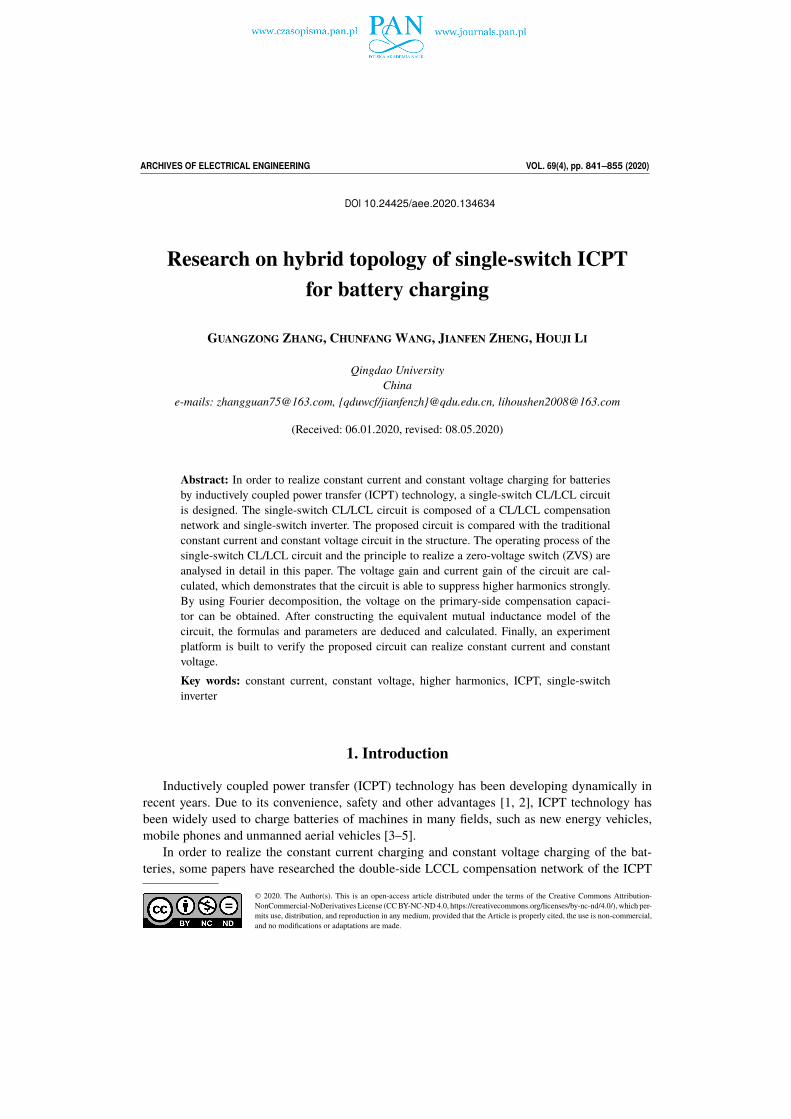
conversion. It generates a high-frequency alternating magnetic field with alternating current inthe primary-side coil of a loosely coupled transformer, and then generates induced electromotiveforce on the secondary-side coil of the loosely coupled transformer to achieve the purpose ofenergy transmission. As the SP/PP hybrid circuit is shown in Fig. 1, Uin is the power supply,Cin is the input filter capacitor, and Q1, Q2, Q3 and Q4 are the switches of a full-bridge circuit.By controlling the on-off of switches Q5, Q6 and Q7, the primary side of the circuit can realizeseries compensation or parallel compensation. M is the mutual inductance of a loosely coupledtransformer. The Ls and Cs are connected in parallel to construct a parallel compensation structure.Finally, they are connected to the load through a rectifier bridge.
The working principle of the circuit is that when the switch Q6 is turned off, Q5 and Q7are turned on, and the network is the PP structure, which can supply constant current. When
Vol. 69 (2020) Research on hybrid topology of single-switch ICPT for battery charging 843
Uin Cin
Cs
Q1
LX
LpCout
RL
Cp M
Ls
Q2
Q3
Q4
Q6Q7
Q5
Fig. 1. The hybrid topology circuit of SP/PP
the switches Q5 and Q7 are turned off, Q6 is turned on and the compensation network is the SPstructure, which delivers constant voltage.
2.2. The proposed single-switch CL/LCL circuit
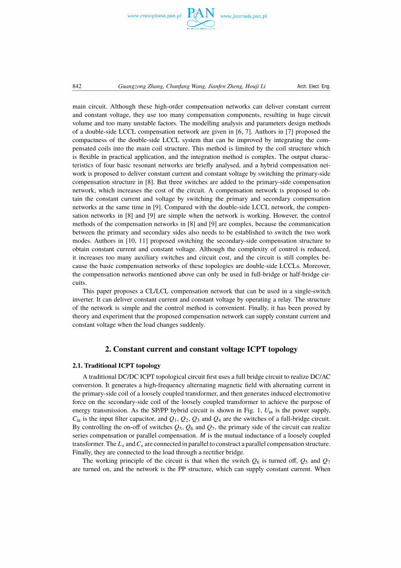
A single-switch circuit is developed from a forward converter and a flyback converter [12, 13].It overcomes the disadvantages that the forward circuit can only transfer power to a secondary-sidecircuit when the switch is turned on and the flyback circuit can only transfer power to a secondary-side circuit when the switch is turned off. Compared with the full-bridge circuit, the single-switchcircuit is simpler and the number of switches is reduced from four to one.
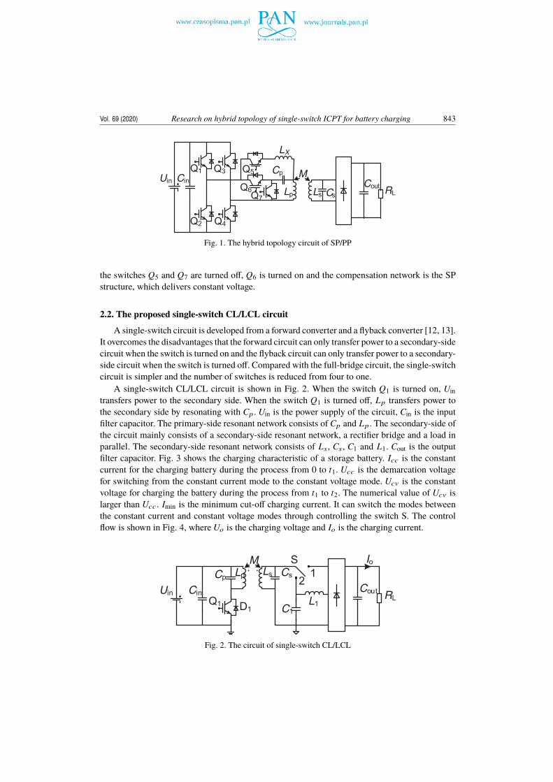
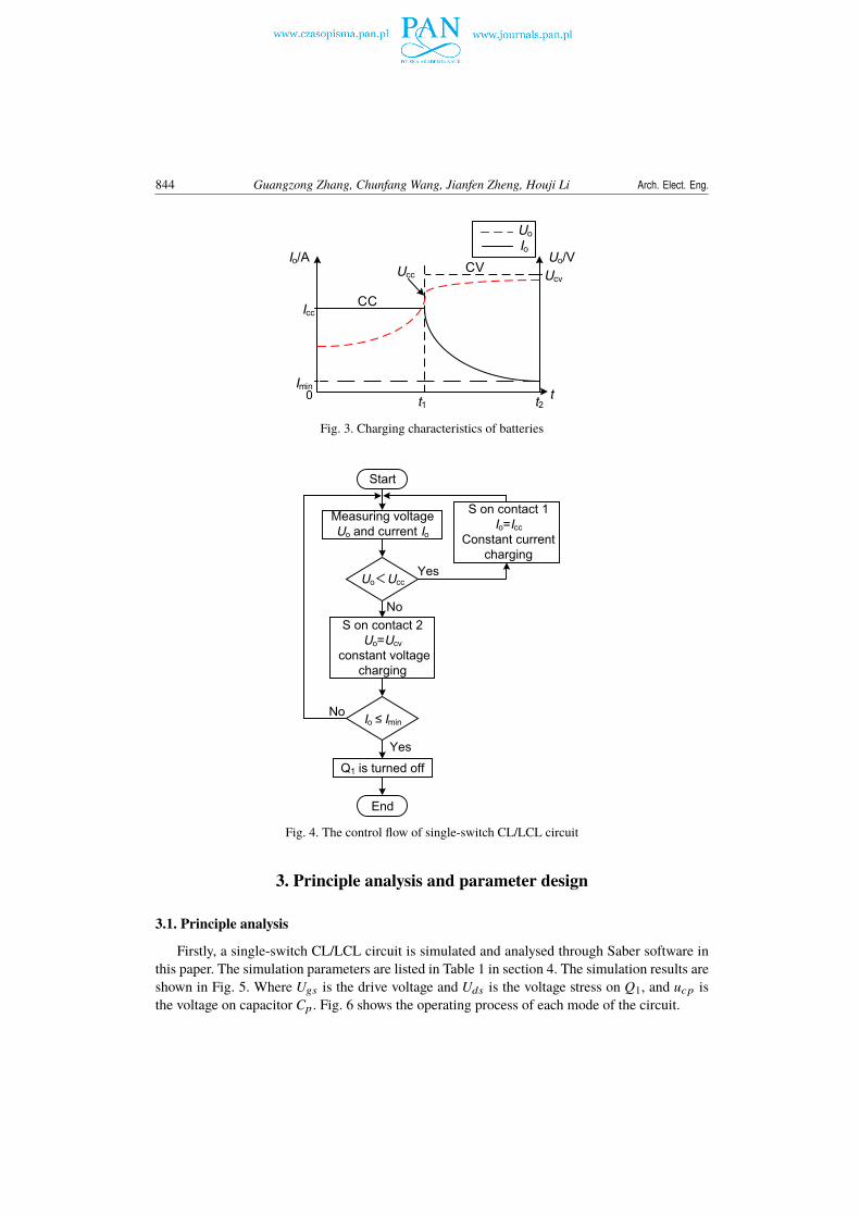
A single-switch CL/LCL circuit is shown in Fig. 2. When the switch Q1 is turned on, Uintransfers power to the secondary side. When the switch Q1 is turned off, Lp transfers power tothe secondary side by resonating with Cp . Uin is the power supply of the circuit, Cin is the inputfilter capacitor. The primary-side resonant network consists of Cp and Lp . The secondary-side ofthe circuit mainly consists of a secondary-side resonant network, a rectifier bridge and a load inparallel. The secondary-side resonant network consists of Ls , Cs , C1 and L1. Cout is the outputfilter capacitor. Fig. 3 shows the charging characteristic of a storage battery. Icc is the constantcurrent for the charging battery during the process from 0 to t1. Ucc is the demarcation voltagefor switching from the constant current mode to the constant voltage mode. Ucv is the constantvoltage for charging the battery during the process from t1 to t2. The numerical value of Ucv islarger than Ucc . Imin is the minimum cut-off charging current. It can switch the modes betweenthe constant current and constant voltage modes through controlling the switch S. The controlflow is shown in Fig. 4, where Uo is the charging voltage and Io is the charging current.
Uin Cin
C1
CoutRL
Cp Cs
Q1 D1
Lp Ls
L1
M Io. .
S
12
Fig. 2. The circuit of single-switch CL/LCL
844 Guangzong Zhang, Chunfang Wang, Jianfen Zheng, Houji Li Arch. Elect. Eng.
t1t
Io/A
0
Uo/V
Imin
Icc
Ucc Ucv
CC
CV
Uo
Io
t2
Fig. 3. Charging characteristics of batteries
Start
Measuring voltage
Uo and current Io
Uo<Ucc
Io ≤ Imin
Yes
Yes
No
S on contact 1
Io=Icc
Constant current
charging
Q1 is turned off
End
S on contact 2
Uo=Ucv
constant voltage
charging
No
Fig. 4. The control flow of single-switch CL/LCL circuit
3. Principle analysis and parameter design
3.1. Principle analysis
Firstly, a single-switch CL/LCL circuit is simulated and analysed through Saber software inthis paper. The simulation parameters are listed in Table 1 in section 4. The simulation results areshown in Fig. 5. Where Ugs is the drive voltage and Uds is the voltage stress on Q1, and ucp isthe voltage on capacitor Cp . Fig. 6 shows the operating process of each mode of the circuit.

Vol. 69 (2020) Research on hybrid topology of single-switch ICPT for battery charging 845
t0
trtr tf tfUgs/V
t
Uds/V
0ucp/V
Uin
t1 t2t3 t5t6t4 t7t
A
0
Fig. 5. The simulated waveform of main circuit
Uin Cin CoutRL
CpCs
Q1 D1
Lp Ls
M Io. .
Uin Cin CoutRL
CpCs
Q1 D1
Lp Ls
M Io. .
(a) (b)
Uin Cin CoutRL
CpCs
Q1 D1
Lp Ls
M Io. .
Uin Cin CoutRL
CpCs
Q1 D1
Lp Ls
M Io. .
(c) (d)
Uin Cin CoutRL
CpCs
Q1 D1
Lp Ls
M Io. .
Uin Cin CoutRL
CpCs
Q1 D1
Lp Ls
M Io. .
(e) (f)
Fig. 6. Operating process of main circuit
The process from 0 to t1, shows the soft switch margin tr of the switch Q1. At the zero time,the voltage on the capacitor Cp is equal to Uin in numerical value, but in the opposite direction.The voltage on switch Q1 is zero, and the current on the inductor Lp continues to pass through theparasitic diode D1 of Q1. The switch is turned on at this time to creates the zero-voltage switch(ZVS) condition.

846 Guangzong Zhang, Chunfang Wang, Jianfen Zheng, Houji Li Arch. Elect. Eng.
During the process from t1 to t2, this duration DT is the turn-on time of the switch. At thetime t1, the state of the Q1 gate is at a high level, and Q1 realizes the ZVS condition. The voltageon the capacitor Cp is still equal to Uin.
During the process from t2 to t3, the switch is turned off. The capacitor Cp starts to chargethe resonant inductor Lp , and ucp declines to zero at the time t3.
During the process from t3 to t4, the switch is turned off. The inductor Lp is charging thecapacitor Cp backward, and ucp is up to the maximum at the time t4.
During the process from t4 to t5, the switch is turned off. The capacitor Cp charges the inductorLp backward, and ucp declines to zero at the time t5.
During the process from t5 to t6, the switch is turned off and the inductor Lp charges thecapacitor Cp forward. ucp increases to the maximum at the time t6, and it is equal to the powersupply voltage Uin. The operating cycle is over.
The operating mode during the process from t6 to t7 is the same as mode during the processfrom 0 to t1. Considering what we have analysed above, it can be seen that the current in the coilLp changes continuously in one operating cycle, and the power is transferred to the secondaryside through the alternating magnetic field.
3.2. Higher harmonic analysis
The mutual inductance equivalent model of the circuit is constructed as shown in Fig. 7. Cp
can be regarded as the equivalent voltage source of the circuit, and the voltage on Cp is ucp . Thenthe mutual inductance equivalent model is transformed into the equivalent model of power supplyas shown in Fig. 8.
C1
Lp-M Ls-M
MCs
Req
L1
ucp
Cs1LT
io
Fig. 7. Mutual inductance equivalent model
[(Lp-M)// M]
+Ls-M Cs C1
Req
L1
i1
Fig. 8. The equivalent transformation circuit of power

Vol. 69 (2020) Research on hybrid topology of single-switch ICPT for battery charging 847
The current gain of the circuit in constant current mode is calculated. The equivalent induc-tance of Lp − M in parallel with M and then in series with Ls − M is as follows:
jωLT =jω(Lp − M
)· M
Lp+ jω
(Lp − M
). (1)
The impedance of LT and Cs are connected in parallel:
Z1 =jωLT
1 − ω2LT · Cs. (2)
The output current in the constant current mode:
iocc =Z1
Z1 + Req·
ucp · Mω2Lp · LT
. (3)
The current gain of the circuit is:Gicc =
iocc
ucp. (4)
To obtain voltage gain under constant voltage mode based on the constant current mode, theonly need is to change the capacitor Cs to Cs1. Then the output current iocv in the constant voltagemode is equal to iocc from (3). The voltage gain of the circuit is:
Gucv =iocv · Req
ucp. (5)
The curves of the current gain in constant current mode and the voltage gain in constant voltagemode are shown in Fig. 9. According to the Saber simulation parameters, when the fundamentalfrequency is 100 kHz , the maximum current and voltage gains are 0.06 and 0.5, respectively. Thecurrent and voltage gains are 3.1 × 10⁻³ and 0.02, respectively, when the frequency is 200 kHz.The gains under other higher harmonics are lower. It can be seen that the topology has a strongability to suppress higher harmonics, thus only the fundamental harmonic can be considered.
2 105
× 4 105
×0
0.15
0.30
0.45
0.60
f1 10
5×
0.02
0.04
0.06
0.08
Zicc f( ) Zucv f( )
Fig. 9. Current gain of constant current mode and voltage gain of constant voltage mode
According to the analysis of the current and voltage gains of the circuit above, it can be seenthat the influence of higher harmonics on the input and output of the circuit can be neglected. Wecan decompose ucp by Fourier decomposition and get the fundamental wave.

848 Guangzong Zhang, Chunfang Wang, Jianfen Zheng, Houji Li Arch. Elect. Eng.
As shown in Fig. 10, the solid line is the waveform of the voltage ucp and the dotted line is thesine wave at the same frequency. ucp can be approximated as a sine wave at the same frequencyfrom the cycle from t2 to t6. The voltage of ucp is:
ucp = Uin (0 − t2)
ucp = A sin (ω1 + ϕ) (t2 − t6). (6)
u/V
0
Uin
A
Fig. 10. The fitting chart of ucp and sine wave
When t2 < t < t3, and t5 < t < t6, combined with Fig. 5 and (6), we can see that:
t f (A) = arcsin(ucp
A
) 1ω1, (7)
whereω1(A) =
2π2 ·
[(1 − D)T − 2t f (A)
] . (8)
ucp can be simplified in the period of t2–t3 and t5–t6 from Fig. 5.
t3∫t2
ucp +
t6∫t5
ucp ≈ t fUin . (9)
The equation group of the variable A, which is the amplitude of ucp is as follows:
f (A) = Uin
[DT + t f (A)
]h(A) =
A√
2
[(1 − D)T − 2t f (A)
] . (10)
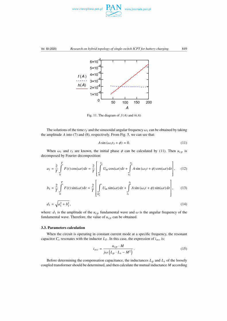
The graph of equation group (10) is shown in Fig. 11. The dotted line refers to the curve ofequation f (A), and the solid line is the curve of equation h(A). The voltage at both ends of thecapacitance Cp and inductance Lp is equal. According to the principle of volt-second balance,the intersection point of the two lines is the solution of the equation group.
Vol. 69 (2020) Research on hybrid topology of single-switch ICPT for battery charging 849
50 100 150 2000
A( )
A( )
A
6 10-4
×
5 10-4
×
4 10-4
×
3 10-4
×
2 10-4
×
1 10-4
×
f
h
Fig. 11. The diagram of f (A) and h(A)
The solutions of the time t f and the sinusoidal angular frequencyω1 can be obtained by takingthe amplitude A into (7) and (8), respectively. From Fig. 5, we can see that:
A sin (ω1t3 + ϕ) = 0. (11)
When ω1 and t3 are known, the initial phase ϕ can be calculated by (11). Then ucp isdecomposed by Fourier decomposition:
a1 =2T
T∫0
F (t) cos(ωt) dt =2T
t3∫
0
Uin cos(ωt) dt +
t5∫t3
A sin (ω1t + ϕ) cos(ωt) dt
, (12)
b1 =2T
T∫0
F (t) sin(ωt) dt =2T
∫0t3
Uin sin(ωt) dt +
t5∫t3
A sin (ω1t + ϕ) sin(ωt) dt
, (13)
d1 =√
a21 + b2
1 , (14)
where: d1 is the amplitude of the ucp fundamental wave and ω is the angular frequency of thefundamental wave. Therefore, the value of ucp can be obtained.
3.3. Parameters calculationWhen the circuit is operating in constant current mode at a specific frequency, the resonant
capacitor Cs resonates with the inductor LT . In this case, the expression of iocc is:
iocc =ucp · M
jω(Lp · Ls − M2
) . (15)
Before determining the compensation capacitance, the inductances Lp and Ls of the looselycoupled transformer should be determined, and then calculate the mutual inductance M according
850 Guangzong Zhang, Chunfang Wang, Jianfen Zheng, Houji Li Arch. Elect. Eng.
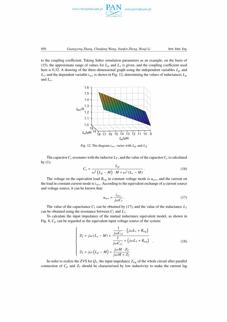
to the coupling coefficient. Taking Saber simulation parameters as an example, on the basis of(15), the approximate range of values for Lp and Ls is given, and the coupling coefficient usedhere is 0.32. A drawing of the three-dimensional graph using the independent variables Lp andLs , and the dependent variable iocc is shown in Fig. 12, determining the values of inductances Lp
and Ls .
916 15 14 13 12 11 101418 17
1.1
1.018
1.6
1.5
1.4
1.3
1.2
Ls/uH
iocc/A
Lp/uH
Fig. 12. The diagram iocc varies with Lp and LS
The capacitor Cs resonates with the inductor LT , and the value of the capacitor Cs is calculatedby (1):
Cs =Lp
ω2(Lp − M
)· M + ω2 (Ls − M)
. (16)
The voltage on the equivalent load Req in constant voltage mode is uocv, and the current onthe load in constant current mode is iocv. According to the equivalent exchange of a current sourceand voltage source, it can be known that:
uocv =iocc
jωC1. (17)
The value of the capacitance C1 can be obtained by (17), and the value of the inductance L1can be obtained using the resonance between C1 and L1.
To calculate the input impedance of the mutual inductance equivalent model, as shown inFig. 8, Cp can be regarded as the equivalent input voltage source of the system:
Z2 = jω (Ls − M) +
1jωCs1
·(jωL1 + Req
)1
jωCs1+(jωL1 + Req
)Z3 = jω
(Lp − M
)+
jωM · Z2
jωM + Z2
. (18)
In order to realize the ZVS for Q1, the input impedance Zeq of the whole circuit after parallelconnection of Cp and Z3 should be characterised by low inductivity to make the current lag
Vol. 69 (2020) Research on hybrid topology of single-switch ICPT for battery charging 851
voltage at a certain angle in the topology. Turning on the reverse-parallel diode D1 of Q1 beforethe arrival of the high level on the gate causes that the sum of voltage on Zeq and Uin is reducedto zero. However, in order to make the whole circuit to operate as close as possible to the zerophase angle, the power factor of the whole system should be considered. Therefore, the selectionof Cp should be compromised between these two conditions.
As for the selection of single switch devices, it can be calculated from the principle analysisin section III and the Kirchhoff voltage law that the voltage stresses on Q1:
Uds = Uin − ucp . (19)
The withstand voltage value of Q1 must be greater than 1.5 times then the peak value of Uds .
4. Experimental analysis
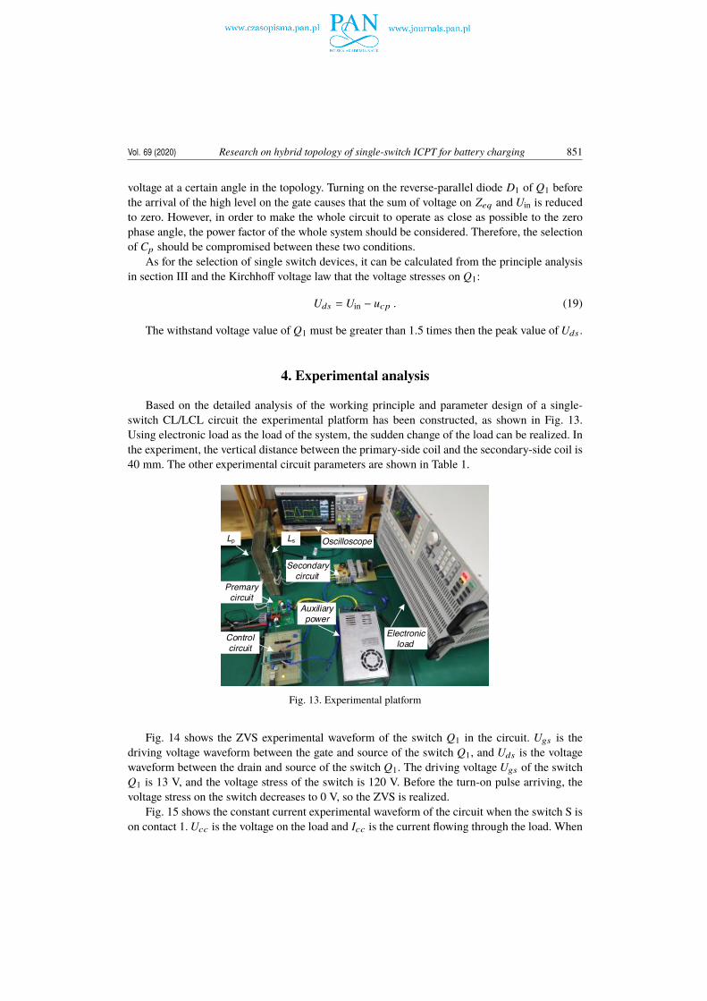
Based on the detailed analysis of the working principle and parameter design of a single-switch CL/LCL circuit the experimental platform has been constructed, as shown in Fig. 13.Using electronic load as the load of the system, the sudden change of the load can be realized. Inthe experiment, the vertical distance between the primary-side coil and the secondary-side coil is40 mm. The other experimental circuit parameters are shown in Table 1.
LsLp
Premary
circuit
Control
circuit
Auxiliary
power
Secondary
circuit
Oscilloscope
Electronic
load
Fig. 13. Experimental platform
Fig. 14 shows the ZVS experimental waveform of the switch Q1 in the circuit. Ugs is thedriving voltage waveform between the gate and source of the switch Q1, and Uds is the voltagewaveform between the drain and source of the switch Q1. The driving voltage Ugs of the switchQ1 is 13 V, and the voltage stress of the switch is 120 V. Before the turn-on pulse arriving, thevoltage stress on the switch decreases to 0 V, so the ZVS is realized.
Fig. 15 shows the constant current experimental waveform of the circuit when the switch S ison contact 1. Ucc is the voltage on the load and Icc is the current flowing through the load. When

852 Guangzong Zhang, Chunfang Wang, Jianfen Zheng, Houji Li Arch. Elect. Eng.
Table 1. Circuit parameters
Parameter Simulation Experimental Parameter Simulation Experimentalvalue value value value
Uin/V 30 30 Cs /nF 180 180
Cin/uF 47 47 C1/nF 180 180
Cp /nF 85 80 L1/uH 13.3 13.1
Lp /uH 16.8 16.1 Cout/uF 47 47
M/uH 5.4 5.2 fs /kHz 100 100
Ls /uH 17.1 16.5
Fig. 14. The ZVS waveform of switch Q1
Fig. 15. The waveform of constant current
Vol. 69 (2020) Research on hybrid topology of single-switch ICPT for battery charging 853
the load changes from 5 Ω to 10 Ω, the voltage rises from 7.5 V to 15 V. and there is a smallfluctuation of the current, but it recovers to 1.5 A as soon as possible and remains stable.
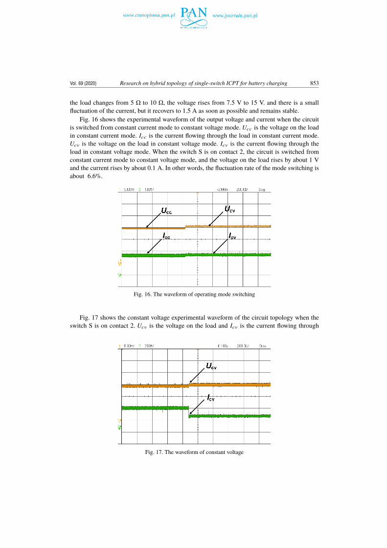
Fig. 16 shows the experimental waveform of the output voltage and current when the circuitis switched from constant current mode to constant voltage mode. Ucc is the voltage on the loadin constant current mode. Icc is the current flowing through the load in constant current mode.Ucv is the voltage on the load in constant voltage mode. Icv is the current flowing through theload in constant voltage mode. When the switch S is on contact 2, the circuit is switched fromconstant current mode to constant voltage mode, and the voltage on the load rises by about 1 Vand the current rises by about 0.1 A. In other words, the fluctuation rate of the mode switching isabout 6.6%.
Fig. 16. The waveform of operating mode switching
Fig. 17 shows the constant voltage experimental waveform of the circuit topology when theswitch S is on contact 2. Ucv is the voltage on the load and Icv is the current flowing through
Fig. 17. The waveform of constant voltage
854 Guangzong Zhang, Chunfang Wang, Jianfen Zheng, Houji Li Arch. Elect. Eng.
the load. When the load changes from 5 Ω to 10 Ω the current on the load decreases from 3 A to1.5 A, and the voltage on the load rises slightly, about 0.2 V and about 1.3%. Then it is stable atabout 15 V.
5. Conclusion
The traditional circuit of constant current and voltage is analysed briefly, and a single-switchCL/LCL circuit is proposed in this paper. The results of the experiment show that the switchQ1 of the proposed circuit can realize a ZVS. When the load is changed abruptly, the outputvoltage is doubled and the fluctuation of the output current is within the allowable range underconstant current mode. When the switching is between constant current and constant voltageoperating modes, the fluctuations of voltage and current are also within the allowable range. Inthe constant voltage operating mode, the output current is reduced by two times, and the outputvoltage fluctuation is also within the allowable range. It can satisfy the constant current chargingin the first stage and the constant voltage charging in the second stage. When the battery is chargedin the third stage, the circuit works in the constant voltage mode. It can stabilize the chargingvoltage and reduce the charging current while the battery power is rising continuously until theend of the whole charging process. The circuit has high practical value, due to the simple structureand control method.
References
[1] Prabhat C.G., Pradip K.S., Ankita G. et al., A new circuit topology using Z-source resonant inverterfor high power contactless power transfer applications, Archives of Electrical Engineering, vol. 66,no. 4, pp. 843–856 (2017).
[2] Liu F., Yang Y., Ding Z. et al., A Multifrequency Superposition Methodology to Achieve High Efficiencyand Targeted Power Distribution for a Multiload MCR WPT System, IEEE Transactions on PowerElectronics, vol. 33, no. 10, pp. 9005–9016 (2018).
[3] Ma G., Jiang L., Chen Y. et al., Study on the impact of electric vehicle charging load on nodal voltagedeviation, Archives of Electrical Engineering, vol. 66, no. 3, pp. 495–505 (2017).
[4] Zhang H.S., Xiao Y.C., Zhong C.Q., Modeling of Mutual Inductance Between Superconducting Pan-cake Coils Used in Wireless Power Transfer (WPT) Systems, IEEE Transactions on Applied Supercon-ductivity, vol. 29, no. 2, pp. 1–4 (2019).
[5] Dai X., Jiang J., Wu J., Charging Area Determining and Power Enhancement Method for Multiexcita-tion Unit Configuration of Wirelessly Dynamic Charging EV System, IEEE Transactions on IndustrialElectronics, vol. 66, no. 5, pp. 4086–4096 (2019).
[6] Li S.Q., Li W.H., Deng J. et al., A Double-Sided LCC Compensation Network and Its Tuning Method forWireless Power Transfer, IEEE Transactions on Vehicular Technology, vol. 64, no. 6, pp. 2261–2273(2015).
[7] Kan T., Nguyen T., White J.C. et al., A New Integration Method for an Electric Vehicle WirelessCharging System Using LCC Compensation Topology: Analysis and Design, IEEE Transactions onPower Electronics, vol. 32, no. 2, pp. 1638–1650 (2017).
[8] Qu X.H., Han H.D., Wong S.C. et al., Hybrid IPT Topologies With Constant Current or ConstantVoltage Output for Battery Charging Applications, IEEE Transactions on Power Electronics, vol. 30,no. 11, pp. 6329–6337 (2015).

Vol. 69 (2020) Research on hybrid topology of single-switch ICPT for battery charging 855
[9] Liu G.J., Bai J.H., Cui Y.L. et al., Double-Sided LCL Compensation Alteration Based on MCR-WPTCharging System, Transactions of China Electrotechnical Society, vol. 34, no. 8, pp. 1569–1579 (2019).
[10] Zhang H., Wang H.M., Li N. et al., Analysis on Hybrid Compensation Topology Circuit for WirelessCharging of Electric Vehicles, Automation of Electric Power Systems, vol. 40, no. 16, pp. 371–75(2016).
[11] Ji L., Wang L.F., Liao C.L. et al., Research and Design of Automatic Alteration between ConstantCurrent Mode and Constant Voltage Mode at the Secondary Side Based on LCL Compensation Networkin Wireless Power Tranfer Systems, Transactions of China Electrotechnical Society, vol. 33, sup. 1,pp. 38–44 (2018).
[12] Kawa A., Penczek A., Pirog S., DC-DC boost-flyback converter functioning as input stage for one phaselow power grid-connected inverter, Archives of Electrical Engineering, vol. 63, no. 3, pp. 393–407(2014).
[13] Liu S., Wang B., Design of quasi-resonant flyback secondary intrinsically safe power supply, Archivesof Electrical Engineering, vol. 68, no. 1, pp. 5–13 (2019).


![12 Switch Zero-Inductor Voltage Converter Topology...Bus Architecture, to achieve this stepdown at high efficiency [6][7]. The topology proposed in this paper is a novel topology for](https://img.pdfslide.net/doc/110x75/5fe7a75918fdc7779a057bf3/12-switch-zero-inductor-voltage-converter-topology-bus-architecture-to-achieve.jpg)