Embed Size (px)
Citation preview
7/31/2019 Research presentation on Si-nanowire based inverter
http://slidepdf.com/reader/full/research-presentation-on-si-nanowire-based-inverter 1/14
Dependence of the Propagation Delay ofSilicon Nanowire Metal-Oxide-Semiconductor
Field-Effect Transistors on Some ImportantParameters
Department of Electronics Engineering
Indian School of Mines
Dhanbad, Jharkhand
India
Subindu Kumar & Dharamvir Kumar([email protected]) ([email protected])
ICONE 2011
7/31/2019 Research presentation on Si-nanowire based inverter
http://slidepdf.com/reader/full/research-presentation-on-si-nanowire-based-inverter 2/14
ICONE 20112
INTRODUCTION
In recent years, Silicon nanowire (SiNW) metal-oxide-
semiconductor field-effect transistors (MOSFETs) hasemerged as one of the most promising structures to extendthe scaling of CMOS devices.
In addition to the effective suppression of short channeleffects, the SiNW MOSFETs with multiple gates show
excellent current drive and they are also compatible withconventional CMOS processes.
Recently, CMOS compatible multi channel SiNW MOSFETs having diameters ≤ 5 nm have been demonstrated with excellent performance .
Due to the enhanced electronic properties of nanowires, SiNWbased inverters show better performance than their planarcounterpart.
7/31/2019 Research presentation on Si-nanowire based inverter
http://slidepdf.com/reader/full/research-presentation-on-si-nanowire-based-inverter 3/14
As one of the most important performance parameters inCMOS digital circuits, propagation delay is of concern todesigners and users.
Both the speed/frequency and dynamic power dissipation of acircuit are affected by propagation delay, so timing analysishas been investigated for several decades.
There is no well-established compact model to capture thetransient characteristics of circuits based on ultrasmallnanoscale devices.
In this paper, we first discuss a simple method for
calculating the average propagation delay in SiNW basedCMOS inverters and then show the dependence of thepropagation delay of these inverters on some importantparameters, such as, thickness of the oxide (insulator),wire dimension, number of channels, and so on, fordifferent load capacitances.
ICONE 2011 3
INTRODUCTION
7/31/2019 Research presentation on Si-nanowire based inverter
http://slidepdf.com/reader/full/research-presentation-on-si-nanowire-based-inverter 4/14
THEORETICAL DETAILS
ICONE 2011 4
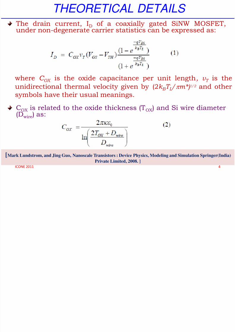
The drain current, ID of a coaxially gated SiNW MOSFET,under non-degenerate carrier statistics can be expressed as:
COX is related to the oxide thickness (T OX) and Si wire diameter(Dwire) as:
where C OX is the oxide capacitance per unit length, v T is theunidirectional thermal velocity given by (2k B T L / m*) 1/2 and other
symbols have their usual meanings.
[Mark Lundstrom, and Jing Guo, Nanoscale Transistors : Device Physics, Modeling and Simulation Springer(India)
Private Limited, 2008. ]
7/31/2019 Research presentation on Si-nanowire based inverter
http://slidepdf.com/reader/full/research-presentation-on-si-nanowire-based-inverter 5/14
ICONE 2011 5
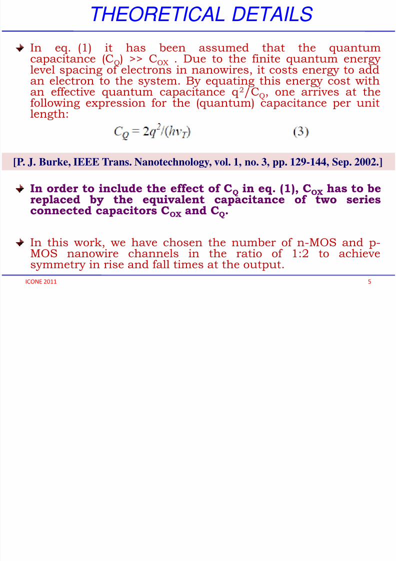
In eq. (1) it has been assumed that the quantumcapacitance (CQ) >> COX . Due to the finite quantum energy
level spacing of electrons in nanowires, it costs energy to addan electron to the system. By equating this energy cost withan effective quantum capacitance q 2/CQ, one arrives at thefollowing expression for the (quantum) capacitance per unitlength:
In order to include the effect of CQ in eq. (1), COX has to bereplaced by the equivalent capacitance of two seriesconnected capacitors COX and CQ.
In this work, we have chosen the number of n-MOS and p-MOS nanowire channels in the ratio of 1:2 to achievesymmetry in rise and fall times at the output.
[P. J. Burke, IEEE Trans. Nanotechnology, vol. 1, no. 3, pp. 129-144, Sep. 2002.]
THEORETICAL DETAILS
7/31/2019 Research presentation on Si-nanowire based inverter
http://slidepdf.com/reader/full/research-presentation-on-si-nanowire-based-inverter 6/14
ICONE 2011 6
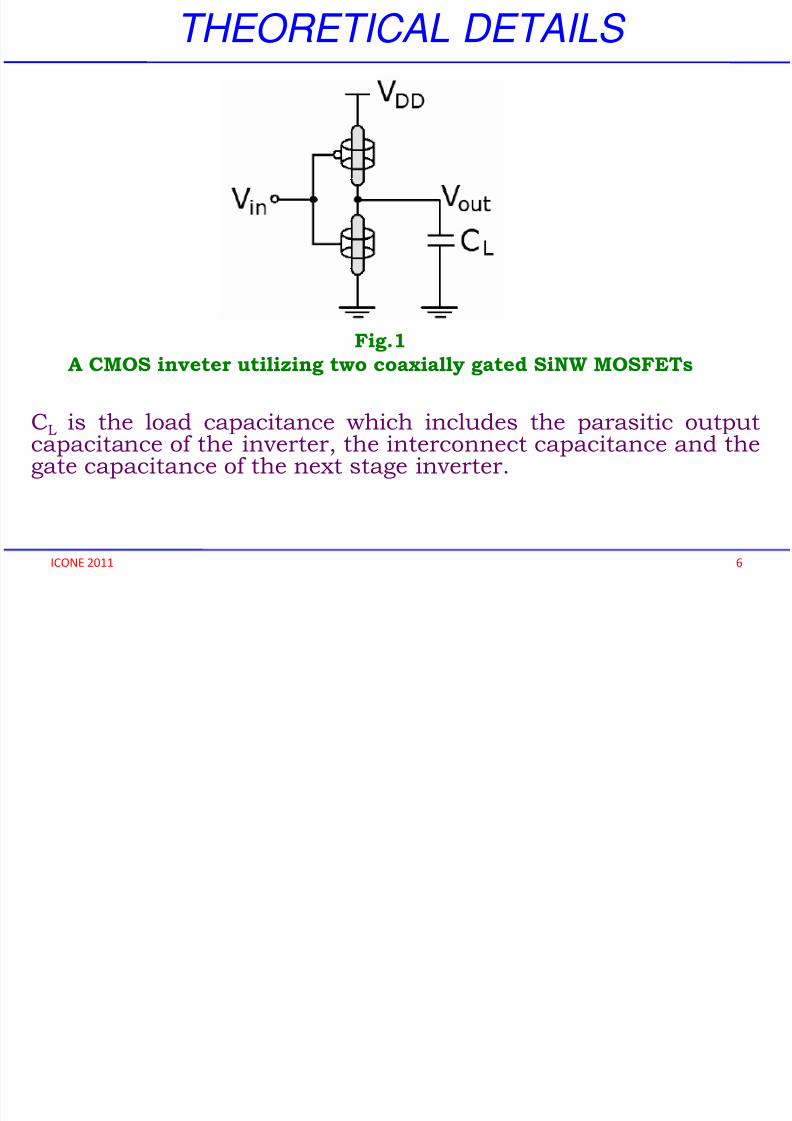
CL is the load capacitance which includes the parasitic outputcapacitance of the inverter, the interconnect capacitance and thegate capacitance of the next stage inverter.
Fig.1
A CMOS inveter utilizing two coaxially gated SiNW MOSFETs
THEORETICAL DETAILS

7/31/2019 Research presentation on Si-nanowire based inverter
http://slidepdf.com/reader/full/research-presentation-on-si-nanowire-based-inverter 7/14
ICONE 2011 7
The propagation delay, tp of a CMOS inverter is given by:
t p = (t PHL + t PLH )/2 (4)
Where tPHL = ln(2).τn is the output fall time from VDD to VDD/2 tPLH = ln(2).τp is the output rise time from 0 V to VDD/2
And τ n(p) = R avg,n(p ) .C L is the time constant related to the
discharging (and charging) of the n-MOS(p-MOS)
respectively, and
R avg, n(p) = Average resistance offered by the n-MOS (p-MOS) during the discharging(and charging) of
the load capacitance.
[John P. Uyemura, Introduction to VLSI Circuits and Systems, Wiley
India, 2006.]
THEORETICAL DETAILS
7/31/2019 Research presentation on Si-nanowire based inverter
http://slidepdf.com/reader/full/research-presentation-on-si-nanowire-based-inverter 8/14
ICONE 2011 8
RESULTS AND DISCUSSIONS
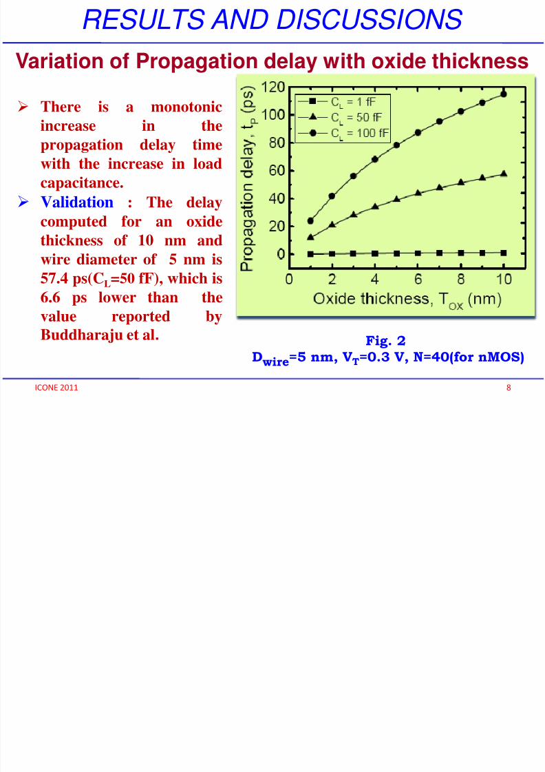
Variation of Propagation delay with oxide thickness
There is a monotonic
increase in the
propagation delay time
with the increase in load
capacitance. Validation : The delay
computed for an oxide
thickness of 10 nm and
wire diameter of 5 nm is
57.4 ps(CL=50 fF), which is6.6 ps lower than the
value reported by
Buddharaju et al. Fig. 2
Dwire=5 nm, VT=0.3 V, N=40(for nMOS)
7/31/2019 Research presentation on Si-nanowire based inverter
http://slidepdf.com/reader/full/research-presentation-on-si-nanowire-based-inverter 9/14
ICONE 2011 9
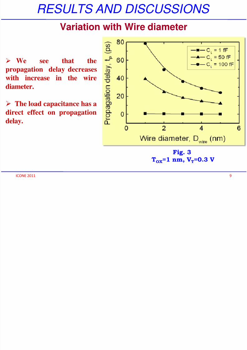
Variation with Wire diameter
We see that the
propagation delay decreases
with increase in the wire
diameter.
The load capacitance has a
direct effect on propagation
delay.
Fig. 3
TOX=1 nm, VT=0.3 V
RESULTS AND DISCUSSIONS
7/31/2019 Research presentation on Si-nanowire based inverter
http://slidepdf.com/reader/full/research-presentation-on-si-nanowire-based-inverter 10/14
ICONE 2011 10
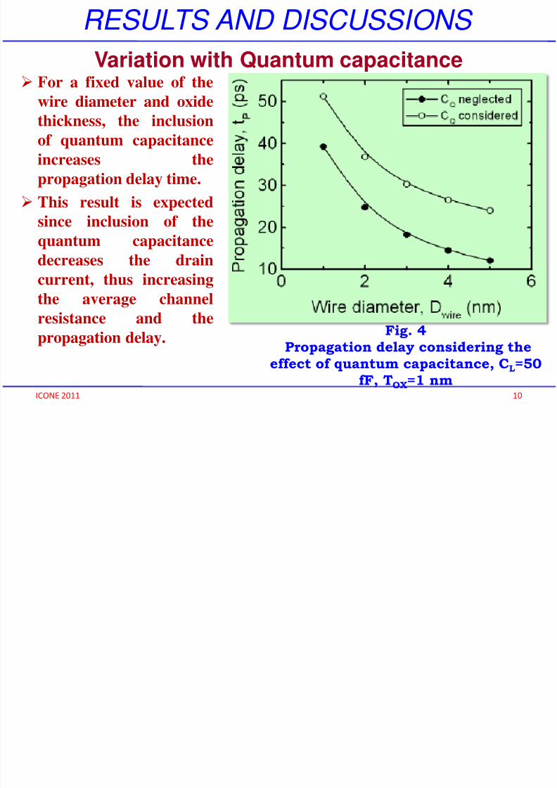
Variation with Quantum capacitance For a fixed value of the
wire diameter and oxidethickness, the inclusion
of quantum capacitance
increases the
propagation delay time.
This result is expected
since inclusion of the
quantum capacitance
decreases the drain
current, thus increasing
the average channel
resistance and the
propagation delay.Fig. 4
Propagation delay considering the
effect of quantum capacitance, CL =50
fF, TOX
=1 nm
RESULTS AND DISCUSSIONS
7/31/2019 Research presentation on Si-nanowire based inverter
http://slidepdf.com/reader/full/research-presentation-on-si-nanowire-based-inverter 11/14
ICONE 2011 11
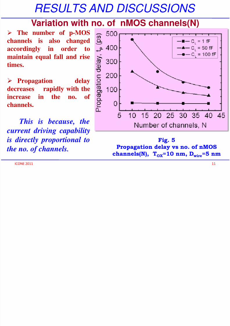
Variation with no. of nMOS channels(N) The number of p-MOS
channels is also changedaccordingly in order to
maintain equal fall and rise
times.
Propagation delaydecreases rapidly with the
increase in the no. of
channels.
This is because, the current driving capability
is directly proportional to
the no. of channels . Fig. 5
Propagation delay vs no. of nMOS
channels(N), TOX=10 nm, Dwire=5 nm
RESULTS AND DISCUSSIONS
7/31/2019 Research presentation on Si-nanowire based inverter
http://slidepdf.com/reader/full/research-presentation-on-si-nanowire-based-inverter 12/14
ICONE 2011 12
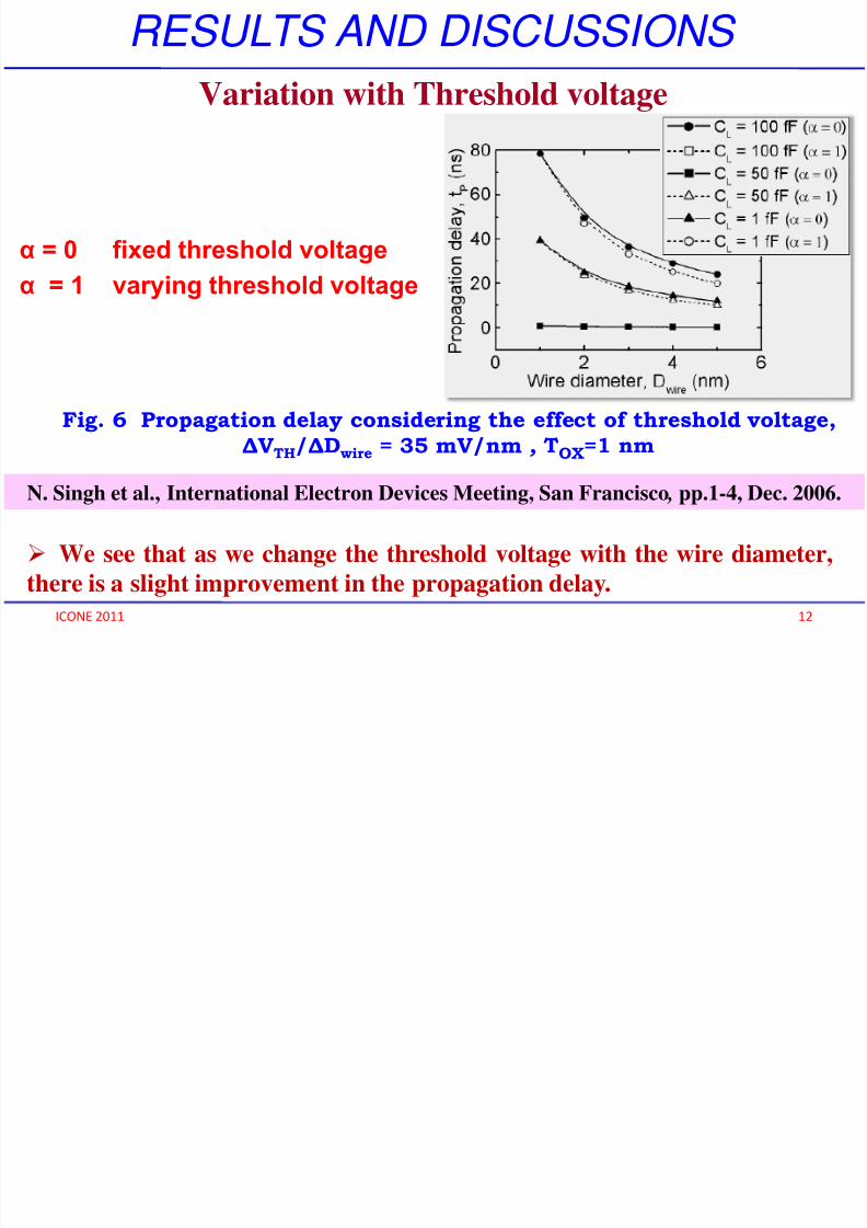
Variation with Threshold voltage
Fig. 6 Propagation delay considering the effect of threshold voltage,
ΔVTH/
ΔDwire = 35 mV/nm , TOX=1 nm
We see that as we change the threshold voltage with the wire diameter,
there is a slight improvement in the propagation delay.
α = 0 fixed threshold voltage
α = 1 varying threshold voltage
RESULTS AND DISCUSSIONS
N. Singh et al., International Electron Devices Meeting, San Francisco , pp.1-4, Dec. 2006.
7/31/2019 Research presentation on Si-nanowire based inverter
http://slidepdf.com/reader/full/research-presentation-on-si-nanowire-based-inverter 13/14
ICONE 2011 13
SUMMARY
We have investigated the effects of some important parameters
such as, SiNW diameter, oxide thickness, quantum capacitance
and number of channels on the propagation delay of CMOS
compatible SiNW based inverters.
The variation of the propagation delay with the thresholdvoltage is also studied.
It was found that the delay decreases significantly if the number
of channels in each n and p-MOS structure increases. The
results obtained are in line with the bench marking data andcould be useful for researchers working in this field.
7/31/2019 Research presentation on Si-nanowire based inverter
http://slidepdf.com/reader/full/research-presentation-on-si-nanowire-based-inverter 14/14
ICONE 2011 14
THANK YOU