Embed Size (px)
Citation preview
Thin Solid Films 425(2003) 145–149
0040-6090/03/$ - see front matter� 2002 Elsevier Science B.V. All rights reserved.PII: S0040-6090Ž02.01287-7
Residual stress induced atomic scale buckling of diamond carboncoatings on silicon substrate
K. Mylvaganam, L.C. Zhang*
School of Aerospace, Mechanical and Mechatronic Engineering, The University of Sydney, Sydney, NSW 2006, Australia
Received 23 April 2002; received in revised form 22 October 2002; accepted 10 December 2002
Abstract
This paper investigates the atomic scale buckling of diamond carbon coatings on silicon substrate caused by residual stressesin two orthogonal directions. It was found that different buckling patterns occurred when the ratio of the residual stresses in thetwo directions were changed. The size of wrinkles increased on going from uniaxial to biaxial compression of the residual stressfields. A telephone-cord like buckling mode took place when the residual stresses were bi-axially equal.� 2002 Elsevier Science B.V. All rights reserved.
Keywords: Buckling; Coatings; Computer simulation; Stress
1. Introduction
Coatings have industrial applications in many engi-neering components. Both soft and hard coatings caninhibit adhesion between the substrate and the counterface resulting in decreased wear. They may also makesurface defects less harmful by moving crack initiationsites from the surface down to subsurface regions, thusimproving the performance of the substrate.Carbon coatings on silicon substrates are very com-
mon. Various techniques such as chemical vapour dep-osition (CVD) and pulse laser deposition are being usedto deposit carbon on to siliconw1x. Depending on thetechnique and conditions, either amorphous carbon filmsor diamond-like carbon films can be produced, of whichthe latter exhibit high density, extreme hardness, highthermal conductivity, chemical inertness, and infraredtransparency. However, the films often suffer from adhe-sion problems—partially or totally delaminated at theinterface or in the substrate due to high compressivestressesw2–13x. For example, Freller et al.w3x showedthat when the compressive stress in a film exceeds theultimate tensile strength of the substrate, failure occursin the substrate. Zehnder et al.w4x reported that a filmdeposited at 208C showed no evidence of failure in the
*Corresponding author. Tel.:q61-2-9351-2835; fax:q61-2-9351-7060.
E-mail address: [email protected](L.C. Zhang).
bulk, but delaminated at the interface, all over thesample. On the other hand, a film grown at 5008Cwould adhere very well to the silicon substrate butwould delaminate when its thickness exceeds 600 nm.Som et al.w5x studied the delamination of CVD diamondfilms deposited on silicon and estimated that the biaxialcompressive stress to initiate the film buckling was 1.19GPa.Bucklingydelamination of a coating is unwanted in
industrial applications. Thus a fundamental understand-ing of the stress relief patterns or buckling modes andthe stress levels at which buckling occurs is necessary.Some very interesting buckling patterns such as tele-phone-cord, sinusoidal wave, sinusoidal shape with extrabranches and a strings-of-beads pattern have been report-ed in Refs.w7,9,10x. Gioia and Ortizw2x have compiledmost of these patterns in their paper on delamination ofcompressed thin films. However, the studies to datehave been mainly using experimental techniques andcontinuum mechanics. Although Pailthorpe et al.w14x,McKenzie et al.w15x, and Rosenblum et al.w16x usedatomistic simulation in their studies on coating theyconcentrated mainly on the energy diffusion, the struc-ture of films and the mismatch-induced residual thermalstresses in filmysubstrate systems.The present study uses molecular dynamics simulation
to investigate the atomic scale buckling modes of dia-mond carbon films deposited on silicon.
146 K. Mylvaganam, L.C. Zhang / Thin Solid Films 425 (2003) 145–149
Fig. 1. The simulation model.
Table 1Parameters for the Morse potentialV(r )sDwe yy2a r yr( )ij 0
ij
2e xya r yr( )ij 0
Parameter Si–C
a (A )y1˚ 4.6417D (kcal mol )y1 100.32r (A)0
˚ 1.9475
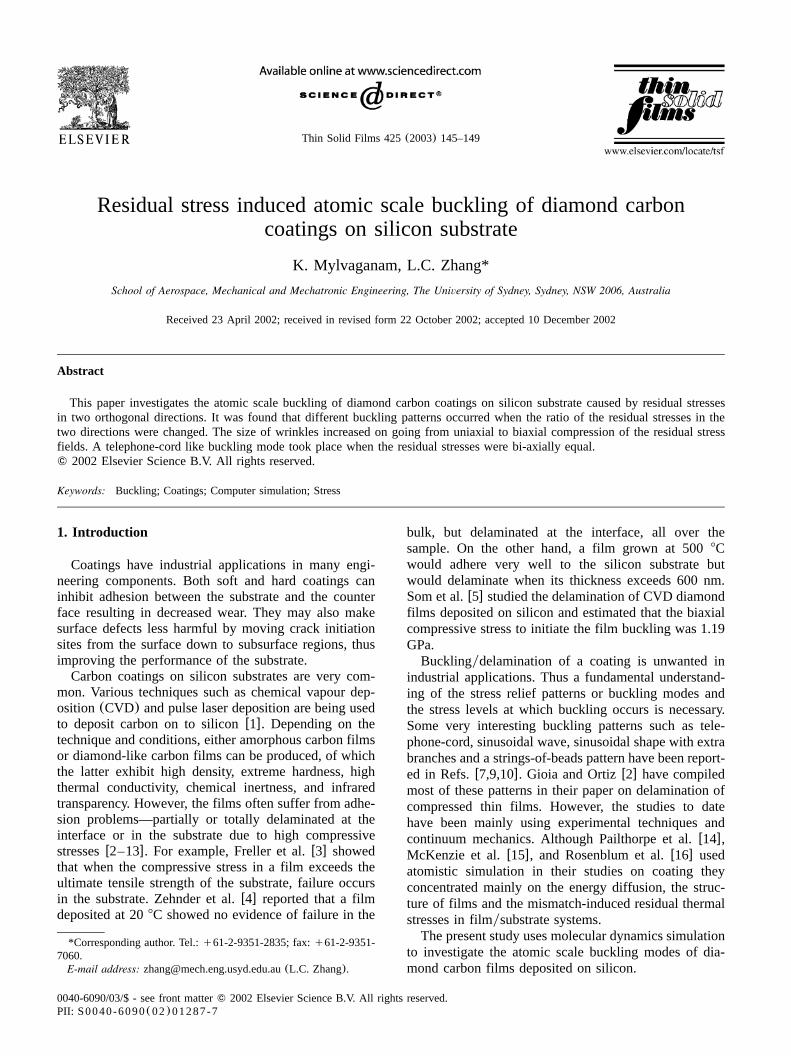
Fig. 2. (a) A cross-section of portion of the film and substrate.(b) Sinusoidal buckling pattern of the top layer of the film inX-direction, afterreleasing the uniaxial stress(s ys s0).y x
2. Simulation method
The buckling of a thin film is caused by localcompressive stresses on the film, introduced by thecoating process. Thorntonw17x pictured this process asfollows: first the incident atoms transfer kinetic energyto the substrate and become loosely bonded ‘ad atoms’.They then diffuse over the surface exchanging energywith the substrate until they are either desorbed ortrapped at low energy sites of the substrate. Thus theinitial kinetic energy transfer to the substrate can induce
a tensile stress on the substrate. When the atoms diffuseover the surface, a compressive stress can be inducedback to the coated atoms. In the present moleculardynamics simulation, for convenience but still capturingthe nature of the residual stress generation, we applythe tensile stresses on the substrate before placing thecoating and then release the stress with the coating on,so that the film will undergo compressions as experi-enced in experiment.We focus on the deformation of a diamond carbon
coating on silicon under various stress levels withdifferent ratios of compressive stresses in two perpen-dicular directions,X andY, as shown in Fig. 1. A pieceof diamond cubic silicon(1 0 0) with the control volumeof 10.3=10.3=3.8 nm (i.e. 19 unit cells=19 unit3
cells=7 unit cells), containing 21 516 atoms, was usedas a substrate. The outermost layer of the substrateatoms with the exception of the top(1 0 0) surface was
147K. Mylvaganam, L.C. Zhang / Thin Solid Films 425 (2003) 145–149
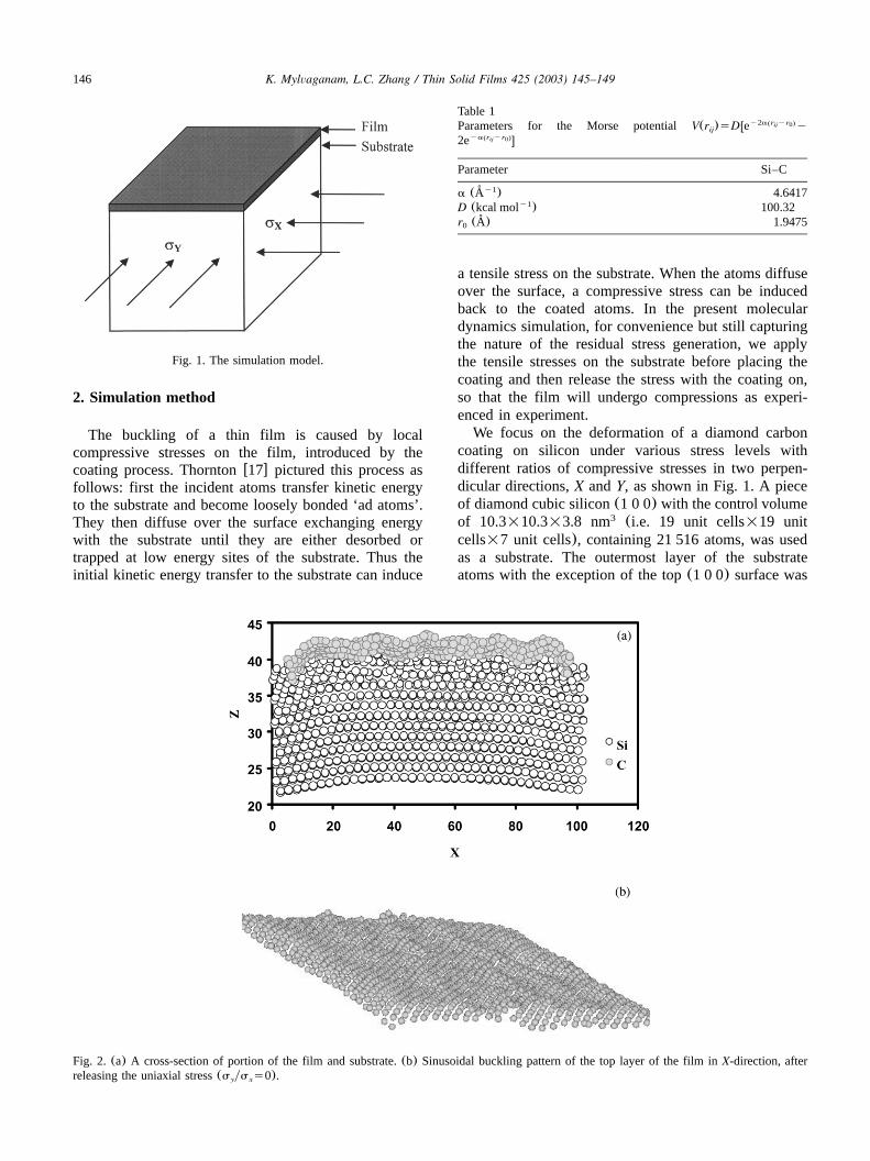
Fig. 3. (a) A cross-section of portion of the film and substrate.(b) Wavy buckling pattern of the top layer of the film, after releasing the biaxialstresses(s ys f0.5).y x
thermo-stated to 300 K. The tensile stresses were appliedby forced atomic displacements at the boundary of thecontrol volume in the following distinct ways to uncoverthe effect of stress variation in the film plane:(i) uni-axially (along theX-direction), i.e. the stress externallyapplied in Y-direction would be zero and hence thestress ratio iss ys s0, (ii) bi-axially with less dis-y x
placement alongY-direction to give the stress ratio ofs ys f0.5, and (iii ) bi-axially with equal displace-y x
ments along bothX- andY-directions to give the stressratio of s ys f1. Three atomic layers of diamondy x
coating with dimensions 9.987=9.987=0.1783 nm ,3
having 4817 atoms was placed on the stressed substrate.The coating and substrate were relaxed together for 5Ps and then the stresses on the substrate were releasedgradually.A three-body Tersoff potentialw18,19x, which has
been used in many successful MD simulation studiesw20–24x, was used for Si–Si and C–C interactions. Atwo-body Morse potential was used for C–Si interac-tions with the parameters shown in Table 1. This
potential has been proved to be reliable in describingC–Si, C–Cu and C–Al interactionsw23–28x. Since thepurpose of this study is to explore the deformationpatterns of the film, to facilitate the observation of thebuckling deformation, we apply sufficiently large stress-es, much higher than the critical buckling stress meas-ured in relevant experimentsw5,7x, provided that theyare within the elastic limit of silicon.
3. Results and discussion
3.1. Observations
3.1.1. Substrate under uniaxial stress (s ys s0)y x
When subjected to a uniaxial stresss , we find thatx
the substrate of mono-crystalline silicon deforms plasti-cally at a Cauchy stress(also known as true stress anddefined as forceycurrent area) of 16.0 GPa. Hence inthe present study the coating was placed on the substratepre-tensioned to 12.5 GPa at which the silicon substratestill deforms elastically. Fig. 2a shows a cross-section
148 K. Mylvaganam, L.C. Zhang / Thin Solid Films 425 (2003) 145–149
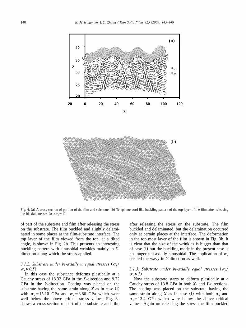
Fig. 4.(a) A cross-section of portion of the film and substrate.(b) Telephone-cord like buckling pattern of the top layer of the film, after releasingthe biaxial stresses(s ys f1).y x
of part of the substrate and film after releasing the stresson the substrate. The film buckled and slightly delami-nated in some places at the film-substrate interface. Thetop layer of the film viewed from the top, at a tiltedangle, is shown in Fig. 2b. This presents an interestingbuckling pattern with sinusoidal wrinkles mainly inX-direction along which the stress applied.
3.1.2. Substrate under bi-axially unequal stresses (s yy
s f0.5)x
In this case the substance deforms plastically at aCauchy stress of 18.32 GPa in theX-direction and 9.72GPa in the Y-direction. Coating was placed on thesubstrate having the same strain alongX as in case(i)with s s15.10 GPa ands s8.86 GPa which werex y
well below the above critical stress values. Fig. 3ashows a cross-section of part of the substrate and film
after releasing the stress on the substrate. The filmbuckled and delaminated, but the delamination occurredonly at certain places at the interface. The deformationin the top most layer of the film is shown in Fig. 3b. Itis clear that the size of the wrinkles is bigger than thatof case(i) but the buckling mode in the present case isno longer uni-axially sinusoidal. The application ofsy
created the wavy inY-direction as well.
3.1.3. Substrate under bi-axially equal stresses (s yy
s f1)x
Now the substrate starts to deform plastically at aCauchy stress of 13.8 GPa in bothX- andY-directions.The coating was placed on the substrate having thesame strain alongX as in case(i) with both s andx
s s13.4 GPa which were below the above criticaly
values. Again on releasing the stress the film buckled
149K. Mylvaganam, L.C. Zhang / Thin Solid Films 425 (2003) 145–149
and delaminated. A cross-section of part of the film andsubstrate is shown in Fig. 4a and the top most layer ofthe film is shown in Fig. 4b. Now it is interesting tonote that the size of the wrinkles becomes larger thanthose in both cases(Sections 3.1.1 and 3.1.2) and theoverall buckling pattern approaches a telephone-cordlike structure as observed in many experiments.
3.2. Discussion
In all the three cases, although the delaminationoccurs at the interface, the film tends to attract a layerof Si atoms. This is because both the C–C interaction(348 kJ mol ) and the C–Si interaction(285y1
kJ mol ) are greater than the Si–Si interaction(176y1
kJ mol ) w29x so that the Si atoms are attracted towardsy1
the C-film when the film possesses a considerablebending rigidity. The results show that within each case,the buckling mode and the size of the wrinkles did notchange significantly, but the pattern became more pro-nounced, on completely releasing the stress. On theother hand, the buckling mode did vary with thes yy
s ratio, from mainly a sinusoidal mode withs ys sx y x
0 to a telephone-cord like structure whens ys f1.y x
4. Conclusions
Thin film buckling does occur on the atomic scalewhen the compressive stresses in a film are sufficientlyhigh. The buckling mode varies withs ys , indicatingy x
that the stress ratio is an important factor that influencesthe nature of the buckling patterns. It is interesting tonote that the pattern of atomic scale buckling of a thinfilm is similar to that observed in micro-scaleexperiments.
Acknowledgments
The authors would like to thank the AustralianResearch Council for the continuous financial support,and the valuable discussion with Dr Y.G. Shen atDepartment of MEEM, City University of Hong Kong.
References
w1x M. Ohring, Materials Science of Thin Films, Academic Press,San Diego, 2002.
w2x G. Gioia, M. Ortiz, Adv. Appl. Mech. 33(1997) 120.w3x H. Freller, A. Hempel, J. Lilge, H.P. Lorenz, Diamond Relat.
Mater. 1(1992) 563.w4x T. Zehnder, J. Balmer, W. Luthy, H.P. Weber, Thin Solid Films
263 (1995) 198.w5x T. Som, S. Bhargava, M. Malhotra, H.D. Bist, V.N. Kulkarni,
S. Kumar, Appl. Phys. Lett. 72(1998) 3014.w6x X.L. Peng, T.W. Clyne, Thin Solid Films 312(1998) 207.w7x S.B. Iyer, K.S. Harshavardhan, V. Kumar, Thin Solid Films
256 (1995) 94.w8x J.W. Ager III, M.D. Drory, Phys. Rev. B 48(1993) 2601.w9x G. Gille, B. Rau, Thin Solid Films 120(1984) 109.
w10x D. Nir, Thin Solid Films 112(1984) 41.w11x B. Audoly, Phys. Rev. Lett. 83(1999) 4124.w12x K.M. Crosby, R.M. Bradley, Phys. Rev. E 59(1999) R2542.w13x P. Peyla, Phys. Rev. E 62(2000) 1501.w14x B.A. Pailthorpe, D. Mitchell, N.S. Bordes, Thin Solid Films
332 (1998) 109.w15x D.R. McKenzie, D. Muller, B.A. Pailthorpe, Phys. Rev. Lett.
67 (1991) 773.w16x I. Rosenblum, J. Adler, S. Brandon, A. Hoffman, Phys. Rev.
B 62 (2000) 2920.w17x J.A. Thornton, Annu. Rev. Mater. Sci. 7(1977) 239.w18x J. Tersoff, Phys. Rev. B 39(1989) 5566.w19x J. Tersoff, Phys. Rev. Lett. 56(1986) 632.w20x J. Belak, D.B. Boercker, I.F. Stowers, Mater. Res. Soc. Bull.
18 (1993) 55.w21x T. Inamura, S. Shimada, N. Takezawa, N. Ikawa, Ann. CIRP
48 (1999) 81.w22x S. Shimada, N. Ikawa, T. Inamura, H. Ohmori, T. Sata, Ann.
CIRP 44(1995) 523.w23x R. Komanduri, N. Chandrasekaran, L.M. Raff, Philos. Mag. B
81 (2001) 1989.w24x L.C. Zhang, H. Tanaka, JSME Int. J. Ser. A 42(1999) 546.w25x W.C.D. Cheong, L.C. Zhang, Nanotechnology 11(2000) 1.w26x L.C. Zhang, H. Tanaka, Tribol. Int. 31(1998) 425.w27x R. Komanduri, N. Chandrasekaran, L.M. Raff, Wear 242
(2000) 60.w28x R. Komanduri, N. Chandrasekaran, L.M. Raff, Wear 240
(2000) 113.w29x D.R. Lide, CRC Handbook of Chemistry and Physics, Chem-
ical Rubber Company Press, Boca Raton, FL, 2000–2001.