Embed Size (px)
Citation preview
Review of Optical Properties of Materials
Review of optics
Absorption in semiconductors: qualitative discussion
Derivation of Optical Absorption Coefficient in Direct Semiconductors
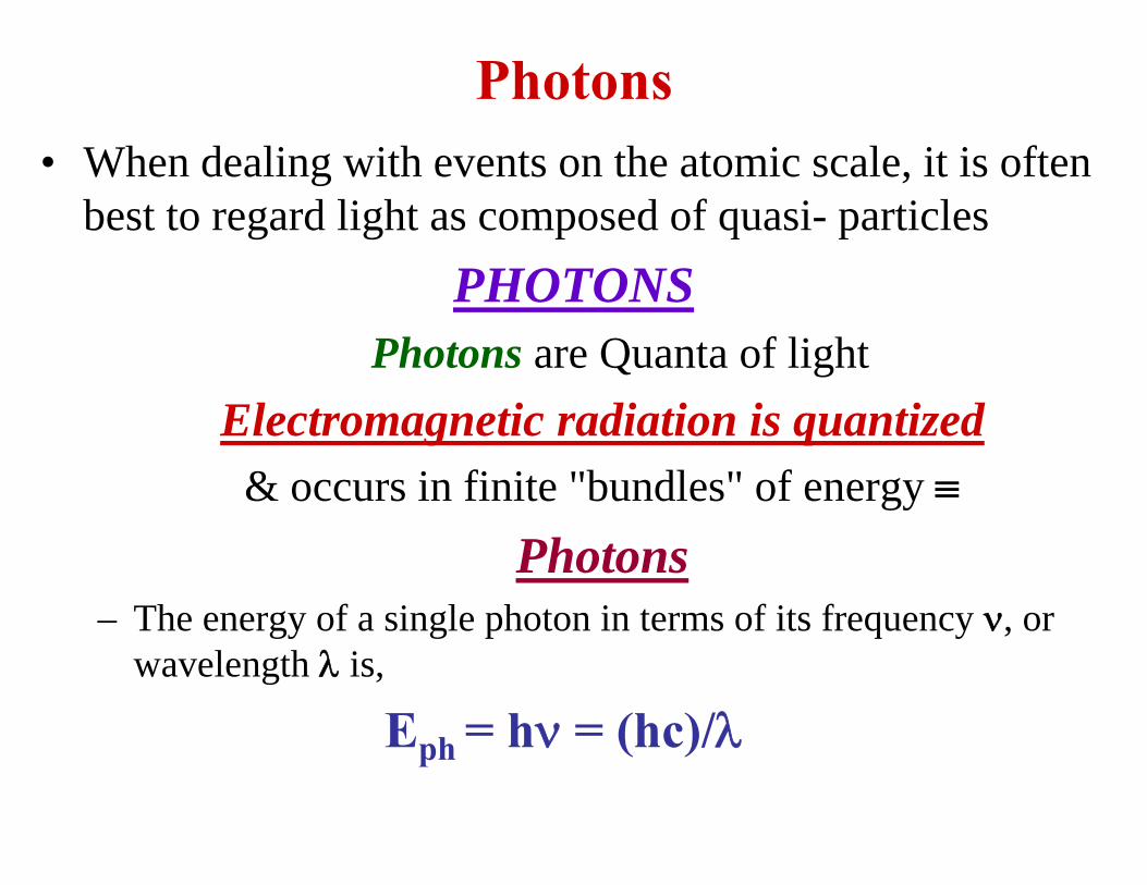
Photons• When dealing with events on the atomic scale, it is often
best to regard light as composed of quasi- particlesPHOTONS
Photons are Quanta of lightElectromagnetic radiation is quantized
& occurs in finite "bundles" of energy
Photons– The energy of a single photon in terms of its frequency , or
wavelength is,
Eph = h = (hc)/
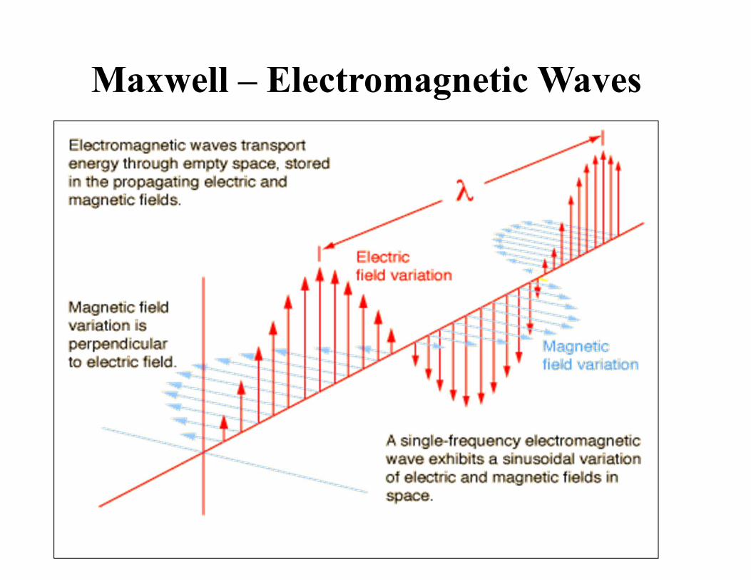
Maxwell – Electromagnetic Waves
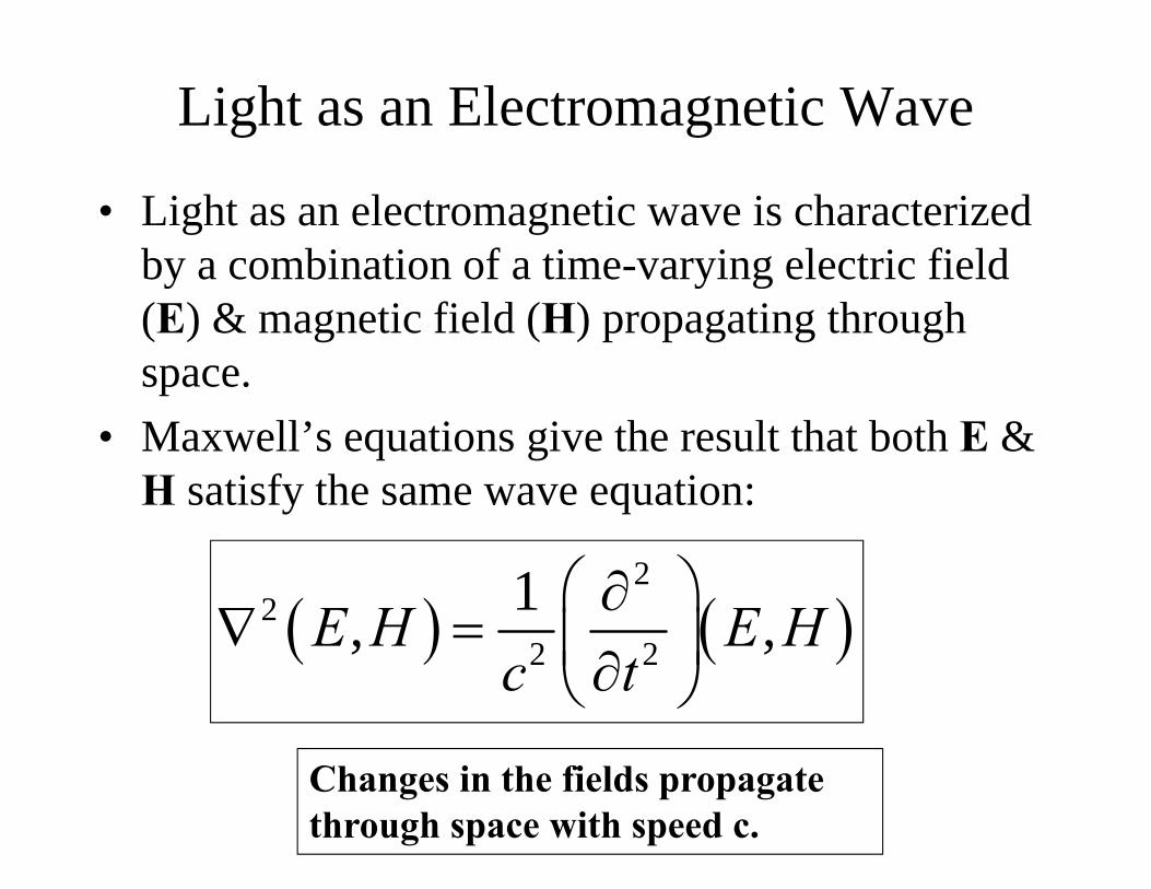
Light as an Electromagnetic Wave
• Light as an electromagnetic wave is characterized by a combination of a time-varying electric field (E) & magnetic field (H) propagating through space.
• Maxwell’s equations give the result that both E & H satisfy the same wave equation:
2
22 2
1, ,E H E Hc t
Changes in the fields propagate through space with speed c.
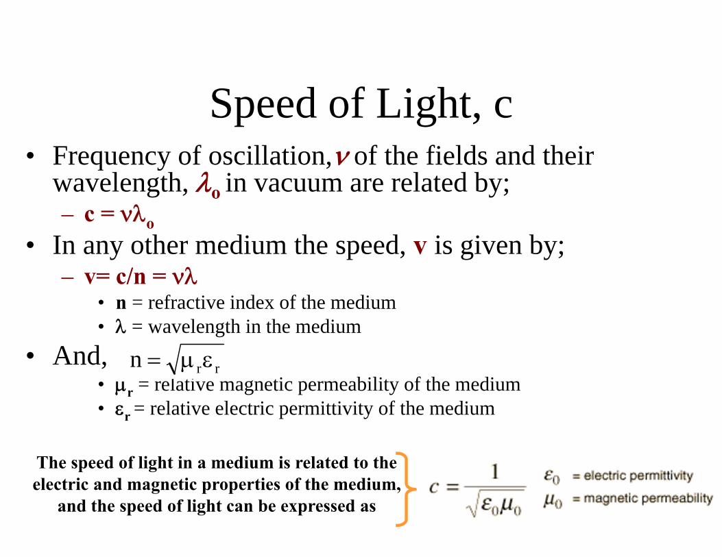
Speed of Light, c• Frequency of oscillation, of the fields and their
wavelength, o in vacuum are related by;– c = o
• In any other medium the speed, v is given by;– v= c/n =
• n = refractive index of the medium • = wavelength in the medium
• And,• r = relative magnetic permeability of the medium • r = relative electric permittivity of the medium
rrn
The speed of light in a medium is related to the electric and magnetic properties of the medium,
and the speed of light can be expressed as
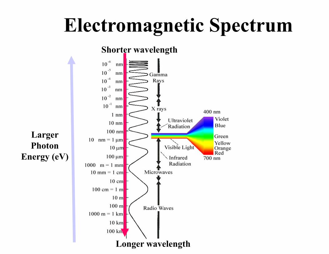
Electromagnetic SpectrumShorter wavelength
Longer wavelength
Larger Photon
Energy (eV)

Scattering
1- Refraction
2- Transmission
3a – Specular reflection
3b – Total internal reflection
3c – Diffused reflection
4 Dispersion –where different colors bend differently
41
3b
2
3a
3c
Incident light
“Semi-transparent” material
Interaction Between Light & Bulk MaterialMany different possible processes can occur!
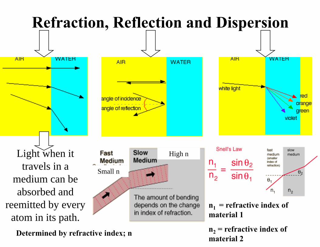
Light when it travels in a
medium can be absorbed and
reemitted by every atom in its path.
Refraction, Reflection and Dispersion
Determined by refractive index; n
Small n
High n
n1 = refractive index of material 1
n2 = refractive index of material 2

Total Internal Reflection
n 2
i
n 1 > n2i
Incidentlight
t
Transmitted(refracted) light
Reflectedlight
k t
i>cc
TIRc
Evanescent wave
k i k r
(a) (b) (c)
Light wave travelling in a more dense medium strikes a less dense medium. Depending onthe incidence angle with respect to c, which is determined by the ratio of the refractiveindices, the wave may be transmitted (refracted) or reflected. (a) i < c (b) i = c (c) i> c and total internal reflection (TIR).
© 1999 S.O. Kasap, Optoelectronics (Prentice Hall)
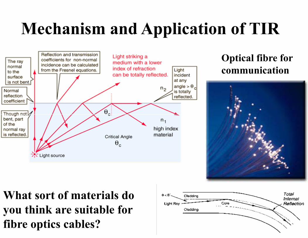
Mechanism and Application of TIROptical fibre for communication
What sort of materials do you think are suitable for fibre optics cables?
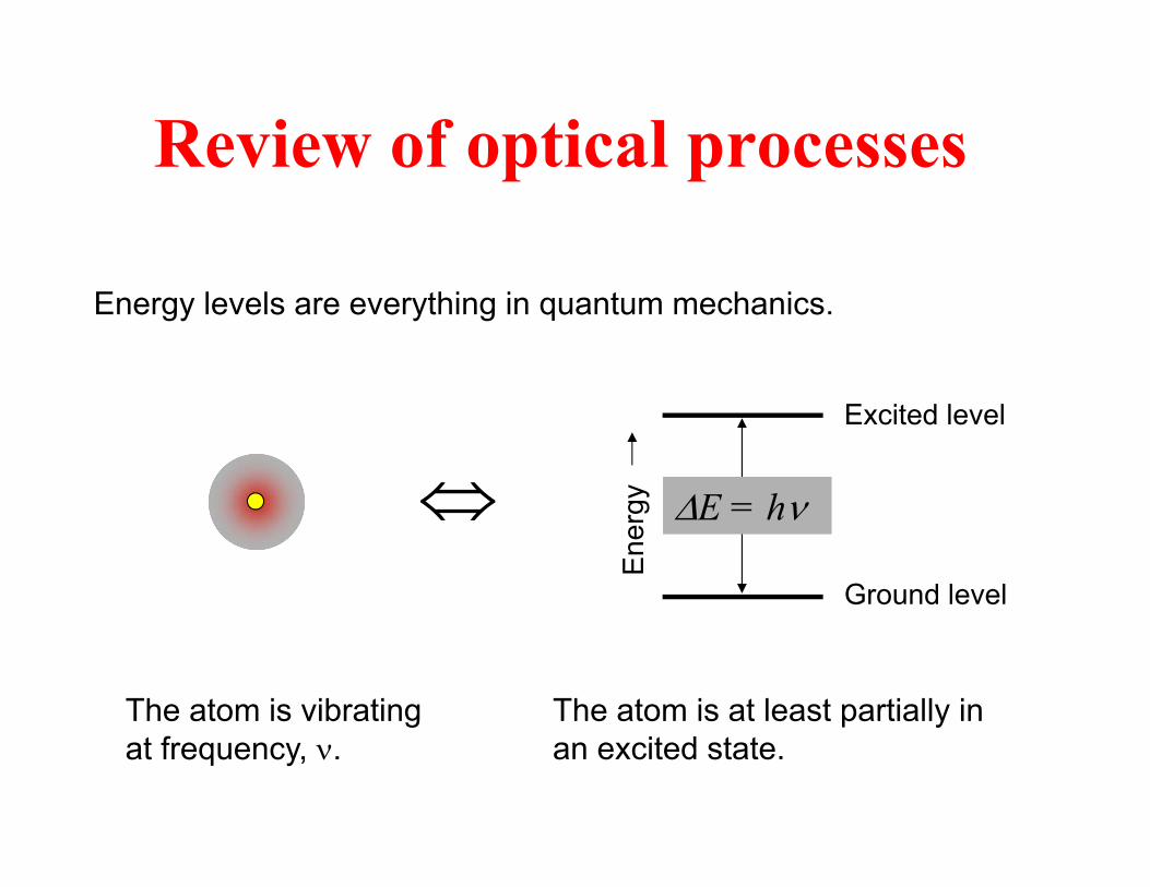
Review of optical processes
Ene
rgy
Ground level
Excited level
E = h
The atom is at least partially in an excited state.
The atom is vibrating at frequency, .
Energy levels are everything in quantum mechanics.
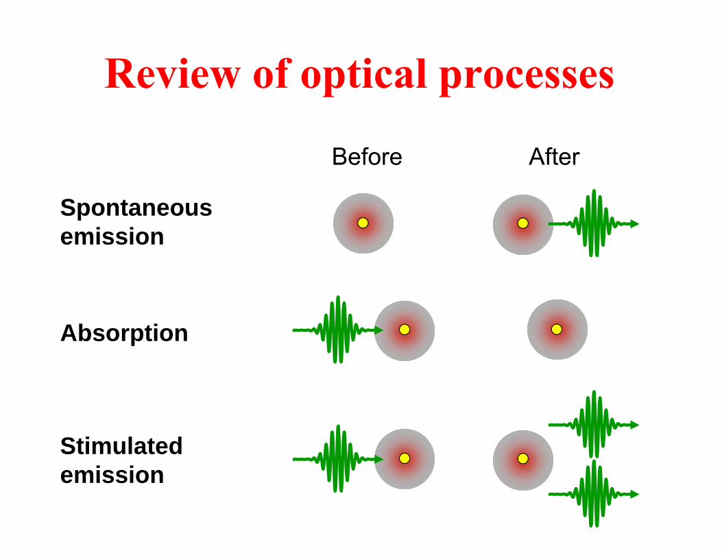
Review of optical processes
Before After
Absorption
Stimulated emission
Spontaneous emission

• Recall: Semiconductor Bandgaps Eg are usually in the range: 0 < Eg < 3 eV
(up to 6 eV if diamond is included)
• Also, at equilibrium, at temperature T = 0, the valence band is full & the conduction band is empty.
• Now, consider what happens if electromagnetic radiation (“light”) is shined on the material.
• In the photon representation of this radiationIf hν Eg, some
electrons can be promoted to the conduction band leaving some holes in the valence band.

• Consider various types of spectra associated with this process:
• Absorption:– Looks at the number of absorbed photons (intensity) vs. photon frequency ω
• Reflection:– Looks at the number of reflected photons (intensity) vs. photon frequency ω
• Transmission:– Looks at the number of transmitted photons (intensity) vs. photon frequency ω
• Emission:– Looks at the number of emitted photons (intensity) vs. photon frequency ω
• Each of these types of spectra are
rich, complicated, & varied!• Understanding such spectra gives
huge amounts of informationabout electronic energy bands, vibrational properties, defects,
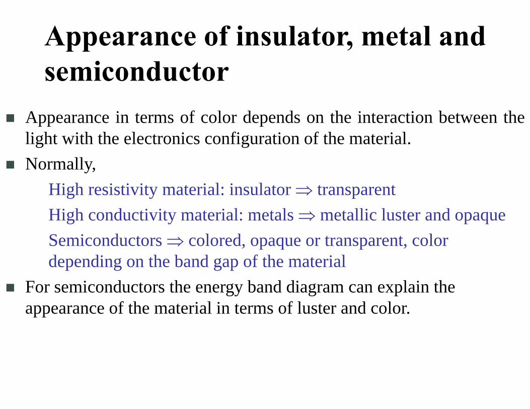
Appearance of insulator, metal and semiconductor
Appearance in terms of color depends on the interaction between thelight with the electronics configuration of the material.
Normally, High resistivity material: insulator transparent High conductivity material: metals metallic luster and opaque Semiconductors colored, opaque or transparent, color
depending on the band gap of the material For semiconductors the energy band diagram can explain the
appearance of the material in terms of luster and color.

Question: Why is Silicon Black and Shiny?
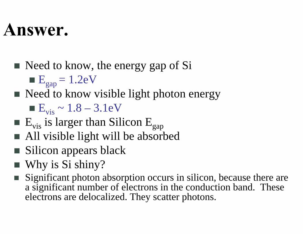
Answer.
Need to know, the energy gap of Si Egap = 1.2eV
Need to know visible light photon energy Evis ~ 1.8 – 3.1eV
Evis is larger than Silicon Egap All visible light will be absorbed Silicon appears black Why is Si shiny? Significant photon absorption occurs in silicon, because there are
a significant number of electrons in the conduction band. These electrons are delocalized. They scatter photons.

Colors of Semiconductors
I B G Y O R
Evis= 1.8eV 3.1eV
•If Photon Energy, Evis > Egap Photons will be absorbed
•If Photon Energy, Evis < Egap Photons will be transmitted
•If Photon Energy is in the range of Egap ;
•Those with higher energy than Egap will be absorbed.
•We see the color of the light being transmitted
•If all colors are transmitted = White
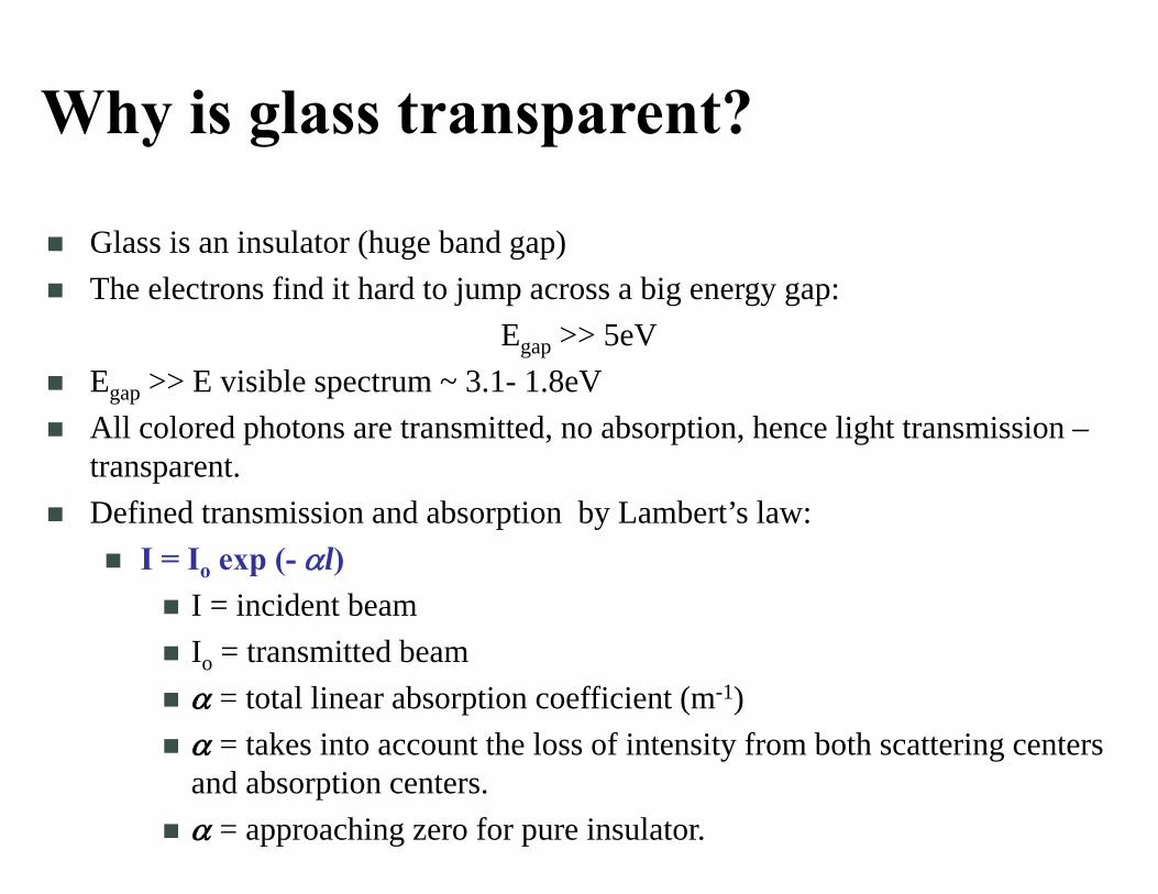
Why is glass transparent?
Glass is an insulator (huge band gap) The electrons find it hard to jump across a big energy gap:
Egap >> 5eV Egap >> E visible spectrum ~ 3.1- 1.8eV All colored photons are transmitted, no absorption, hence light transmission –
transparent. Defined transmission and absorption by Lambert’s law:
I = Io exp (- l) I = incident beam Io = transmitted beam = total linear absorption coefficient (m-1) = takes into account the loss of intensity from both scattering centers
and absorption centers. = approaching zero for pure insulator.

What happens during photon absorption process?
Photon interacts with the lattice
Photon interacts with defects
Photon interacts with valance electrons
Absorption – an important phenomenon in describing optical properties of semiconductors
Light, being a form of electromagnetic radiation,interacts with the electronic structure of atoms of amaterial.
The initial interaction is one of absorption; that is,the electrons of atoms on the surface of a materialwill absorb the energy of the colliding photons oflight and move to the higher-energy states.
The degree of absorption depends, among otherthings, on the number of free electrons capable ofreceiving this photon energy.
Absorption Process of Semiconductors
The interaction process is a characteristic of a photon and depends on the energy of the photon
Low-energy photons interact principally by ionization or excitation of the outer orbitals in solids’ atoms.
Light of low-energy photons (< 10 eV) is represented by infrared (IR), visible light, and ultraviolet (UV) in the electromagnetic spectrum.
High-energy protons (> 104 eV) such as x-rays (and gamma rays) scatter mainly elastically and are used for structure determination
The minimum photon energy required to excite and/or ionize the component atoms of a solid is called the absorption edge or threshold.

Absorption Process of SemiconductorsA
bsor
ptio
n co
effic
ient
(),
cm-1
Photon energy (eV)Absorption spectrum of a semiconductor.
Vis
Eg
~ v
is
Wavelength (m)
IRUV
Important region:
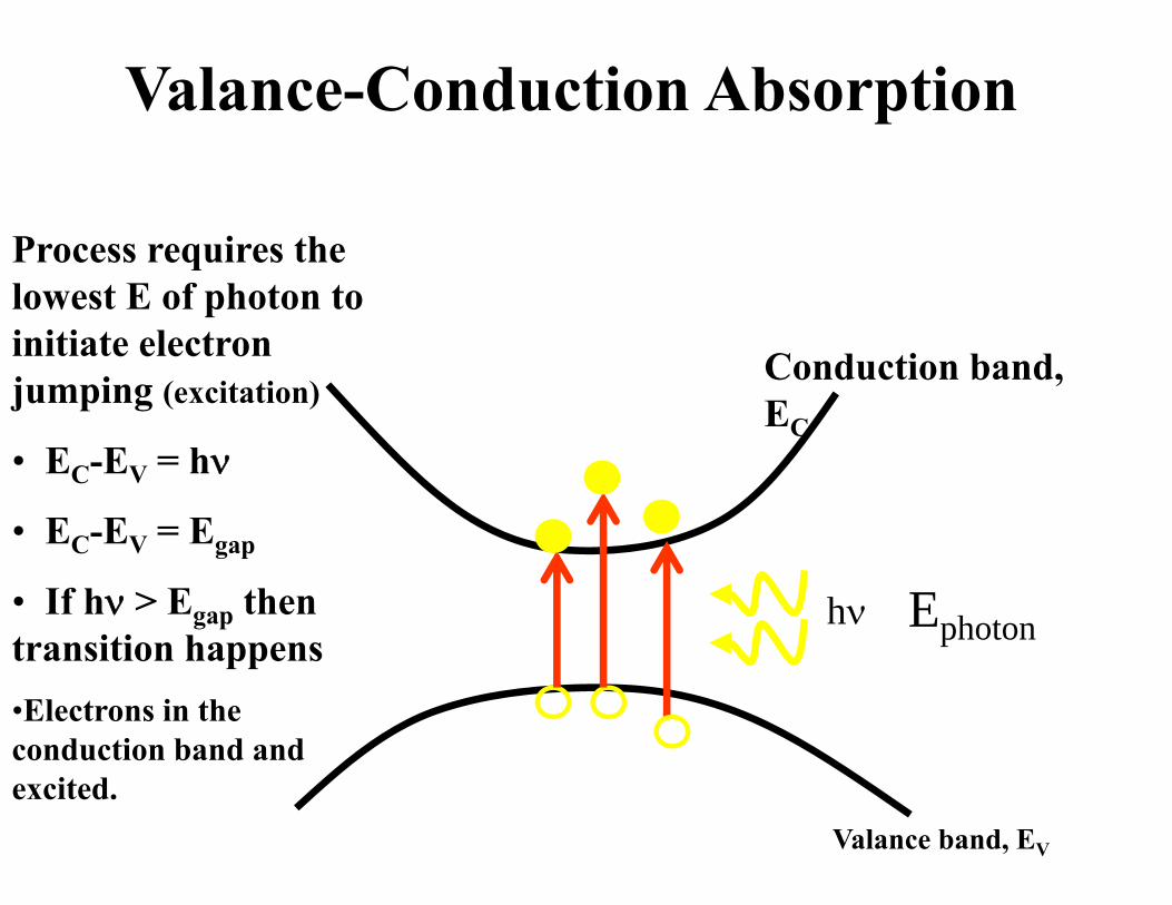
Valance-Conduction Absorption
h
Conduction band, EC
Valance band, EV
EgapEphoton
Process requires the lowest E of photon to initiate electron jumping (excitation)
• EC-EV = h
• EC-EV = Egap
• If h > Egap then transition happens•Electrons in the conduction band and excited.
Absorption
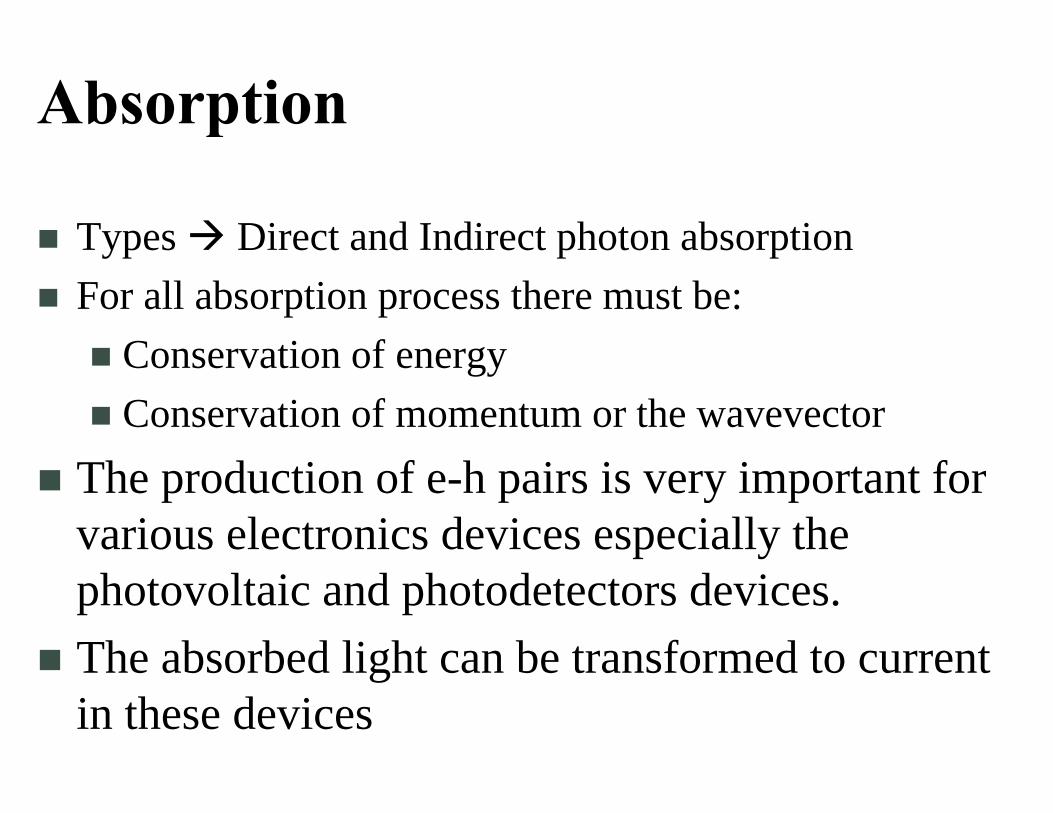
Types Direct and Indirect photon absorption For all absorption process there must be: Conservation of energy Conservation of momentum or the wavevector
The production of e-h pairs is very important for various electronics devices especially the photovoltaic and photodetectors devices.
The absorbed light can be transformed to current in these devices

Direct Band Gap
K (wave number)h
Conservation of E
h = EC(min) - Ev (max) = Egap
Conservation of wavevector
Kvmax + photon = kc
E
Direct vertical transition
Momentum of photon is negligible

Interband absorption in indirect gap semiconductors
Indirect-gap semiconductor: highest occupied and lowest unoccupied state have k≠0
Direct transitions possible for k0 strong direct interband absorption
occurs at E > Egap
Other possibility: momentum and energy can be conserved by photonabsorption and simultaneous absorption or emission of a phonon:
Indirect transitions possible with ‘assistance of a phonon’
Shown here are optically induced transitions
- during phonon emissiona phonon is generated in the process
- during phonon absorptiona phonon is generated in the process
Egap
Egap
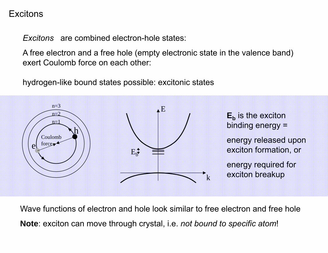
Excitons
Excitons are combined electron-hole states:
A free electron and a free hole (empty electronic state in the valence band)exert Coulomb force on each other:
hydrogen-like bound states possible: excitonic states
eh
Coulomb force
n=3n=2n=1
E
k
Eb
Wave functions of electron and hole look similar to free electron and free hole
Note: exciton can move through crystal, i.e. not bound to specific atom!
Eb is the excitonbinding energy =
energy released uponexciton formation, or
energy required forexciton breakup

Excitonic absorption
Light can excite an electron from the valence band and generate an excitonat energies slightly below the bandgap
see absorption at Ephot = Egap – Eb (absorption slightly below Egap)
Exciton binding energy on the order of a few meVThermal energy at room temperature: kT ~ 25 meV
exciton rapidly dissociates at room temperature absorption lines broaden / disappear for higher temperatures
E
k
Eb
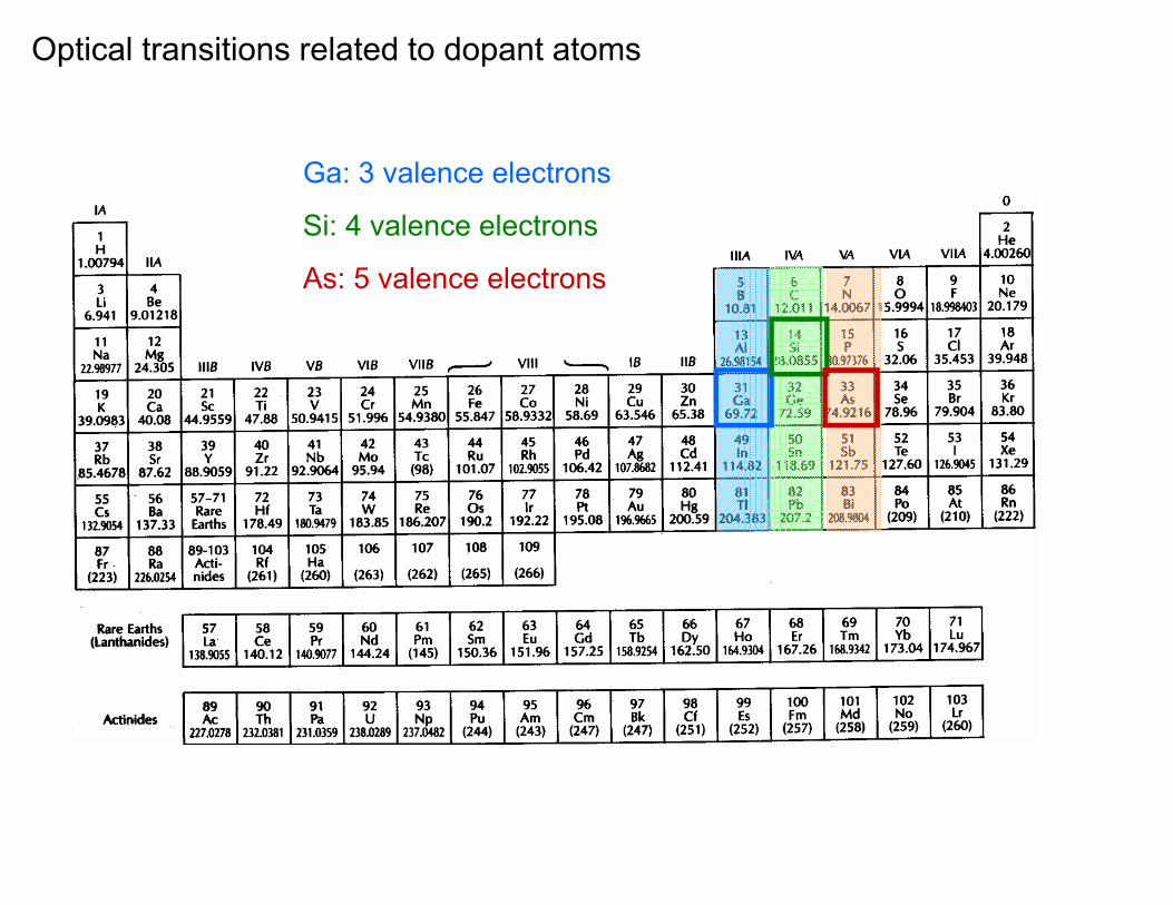
Optical transitions related to dopant atoms
Ga: 3 valence electrons
Si: 4 valence electrons
As: 5 valence electrons
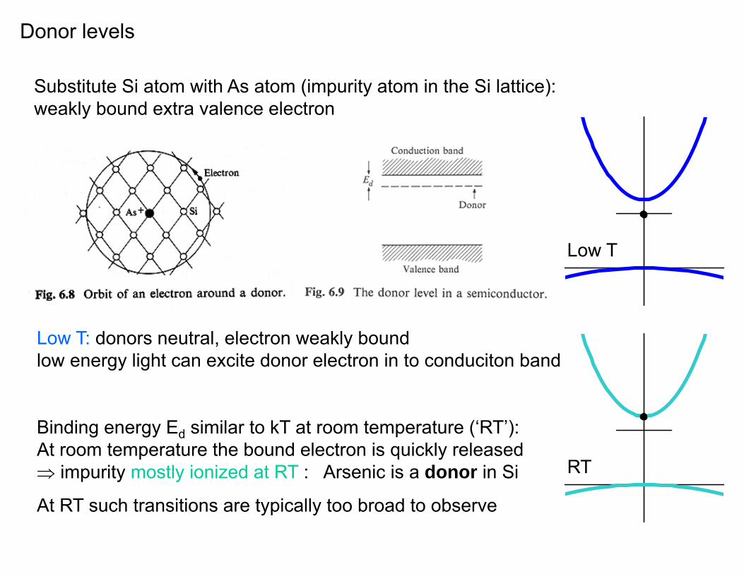
Donor levels
Substitute Si atom with As atom (impurity atom in the Si lattice): weakly bound extra valence electron
Low T: donors neutral, electron weakly boundlow energy light can excite donor electron in to conduciton band
Binding energy Ed similar to kT at room temperature (‘RT’):At room temperature the bound electron is quickly released impurity mostly ionized at RT : Arsenic is a donor in Si
At RT such transitions are typically too broad to observe
Low T
RT
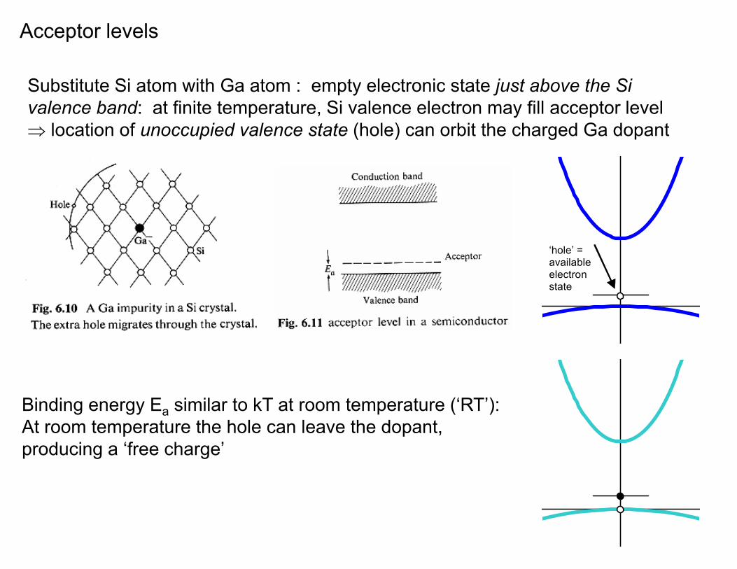
Acceptor levels
Substitute Si atom with Ga atom : empty electronic state just above the Si valence band: at finite temperature, Si valence electron may fill acceptor level location of unoccupied valence state (hole) can orbit the charged Ga dopant
Binding energy Ea similar to kT at room temperature (‘RT’):At room temperature the hole can leave the dopant, producing a ‘free charge’
‘hole’ = available electron state
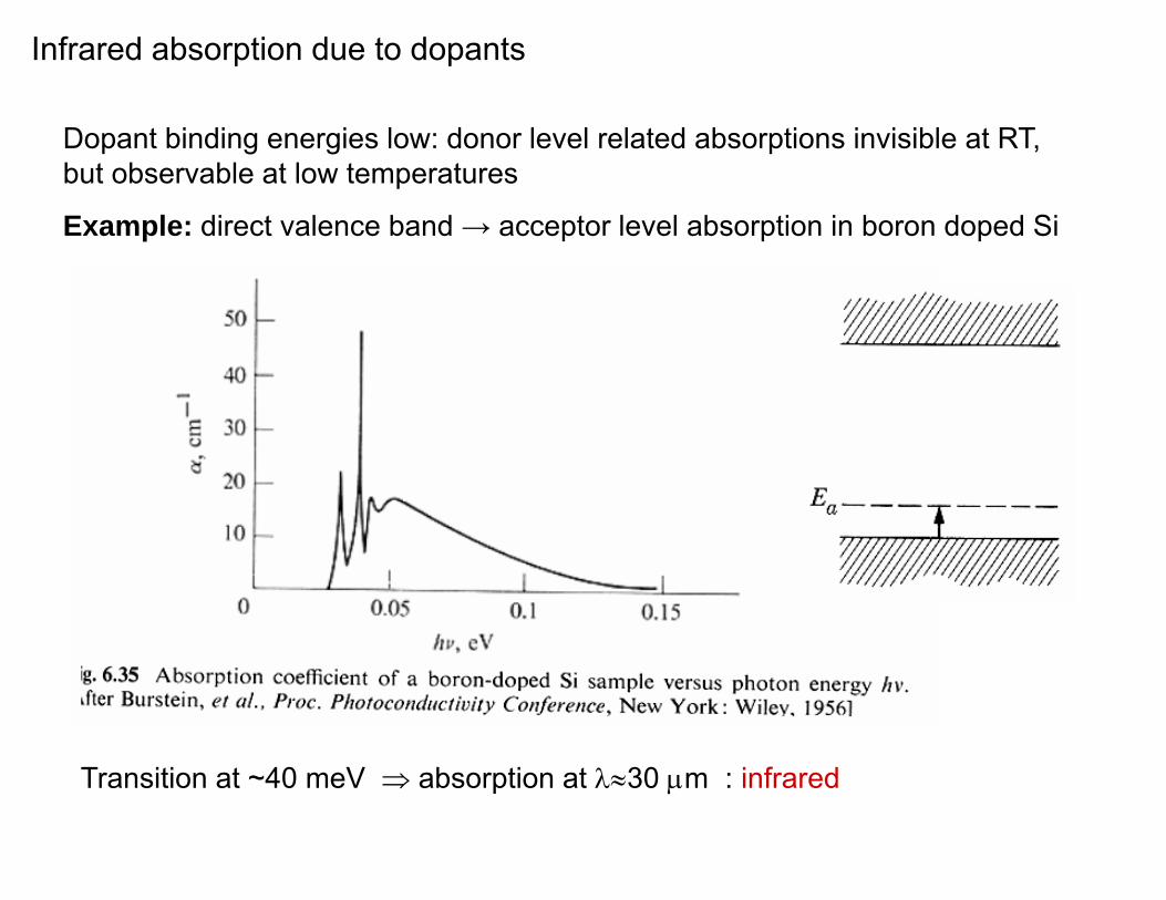
Infrared absorption due to dopants
Dopant binding energies low: donor level related absorptions invisible at RT,but observable at low temperatures
Example: direct valence band → acceptor level absorption in boron doped Si
Transition at ~40 meV absorption at 30 m : infrared
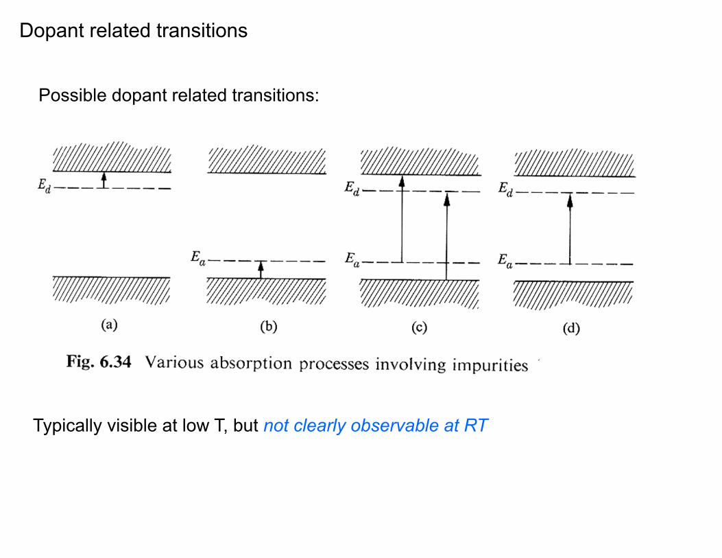
Dopant related transitions
Possible dopant related transitions:
Typically visible at low T, but not clearly observable at RT
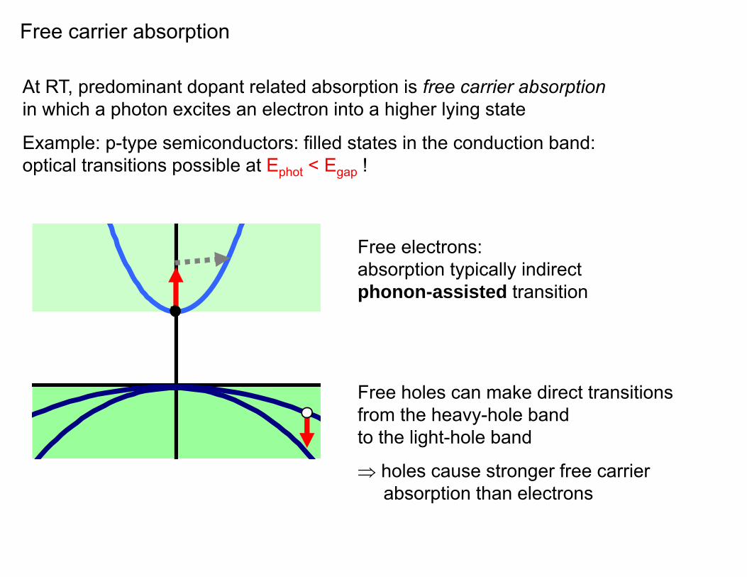
Free carrier absorption
At RT, predominant dopant related absorption is free carrier absorptionin which a photon excites an electron into a higher lying state
Example: p-type semiconductors: filled states in the conduction band:optical transitions possible at Ephot < Egap !
Free electrons: absorption typically indirect phonon-assisted transition
Free holes can make direct transitionsfrom the heavy-hole band to the light-hole band
holes cause stronger free carrier absorption than electrons

Free carrier absorption
Free electron absorption can be described by the Drude model
Dopant levels in semiconductors range from ~1014 - 1018 /cm3
which is ~108 – 104 lower than free electron densities in metals
Plasma frequency of doped semiconductors 104 - 103 lower than of metals: IR
3
2
3
2
2
2
)(",1)('
ppr
pr
2
2
2
2
)(")(p
p
ccc
At frequencies above plasma frequency, εr is complex and is described by
Electron FCA up for lower energies
Free hole absorption less well defined
Derivation of Optical Absorption Coefficient in Direct Semiconductors
Chuang Ch. 9

Outline of derivation
•Absorption Coefficient:
•Examples: lasers, solar cells, etc.
•Fermi’s Golden rulepoly-Si Solar Cells
( )( , ) ( , ) zoI z I z e
( )
•Absorption Coefficient & Simplifications
•Time-dependent perturbation
•Direct-gap net absorption rate

Fermi’s Golden Rule
2'2 ( ( ) ( ))i f fi f i f iW H E E E E
Absorption Emission
Ei
EiEf
Ef

Direct-Gap Net Absorption Rate
22 2 ' 1v c
vc cv c v v ck k
πR H δ(Ε Ε )f fV
Ec
Ev
k
E
Assumptions:kv = kc = k
Undoped, low excitationfv = 1, fc = 0
22 2 'cv c vk
π H δ(Ε Ε )V
Rabs
2 2
*2vh
kEm
2 2
*2c ge
kE Em
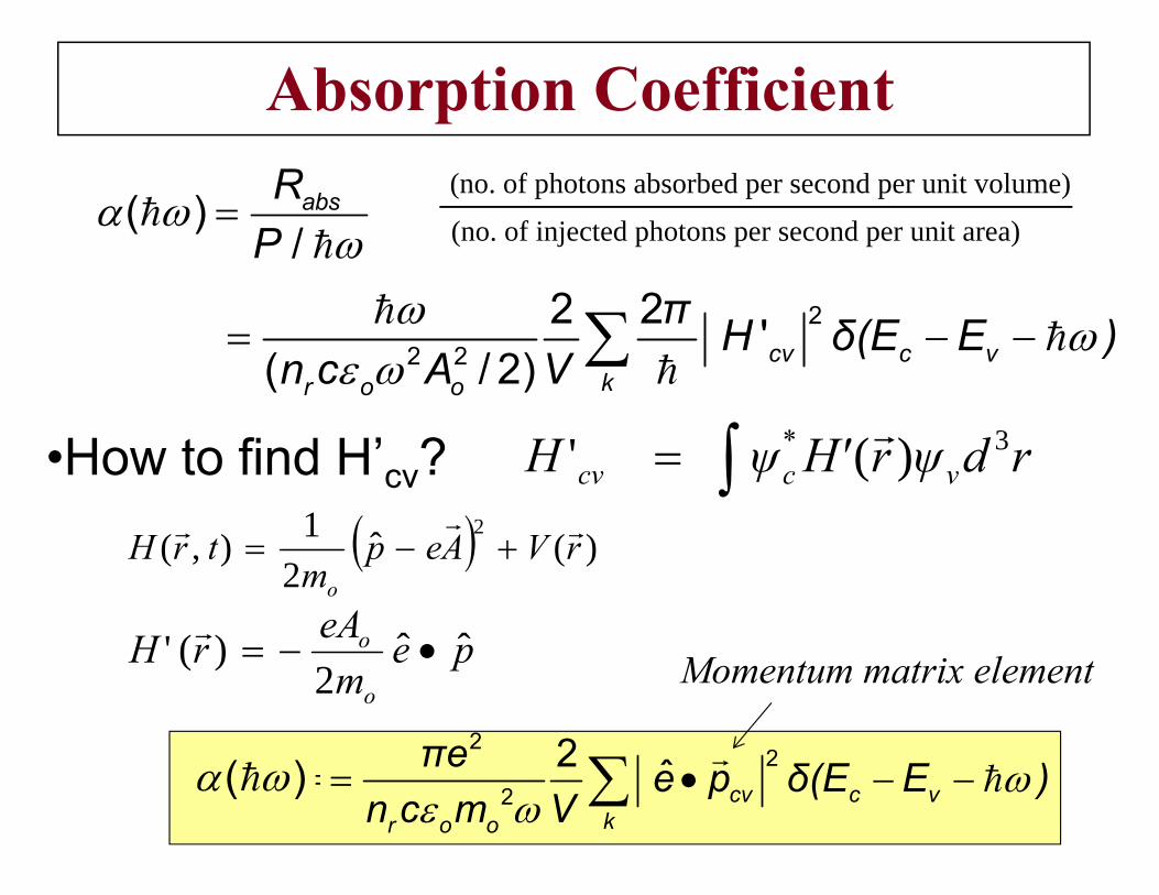
Absorption Coefficient
•How to find H’cv?
( )/absR
P2
2 2
2 2 '( / 2) cv c v
kr o o
π H δ(Ε Ε )n c A V
)(ˆ2
1),(2
rVAepm
trHo
pem
eArHo
o ˆˆ2
)('
rdψrH'ψ H v*ccv
3)('
22
2
2 ˆ cv c vkr o o
πe e p δ(Ε Ε )n c m V
( )
Momentum matrix element
(no. of photons absorbed per second per unit volume)
(no. of injected photons per second per unit area)
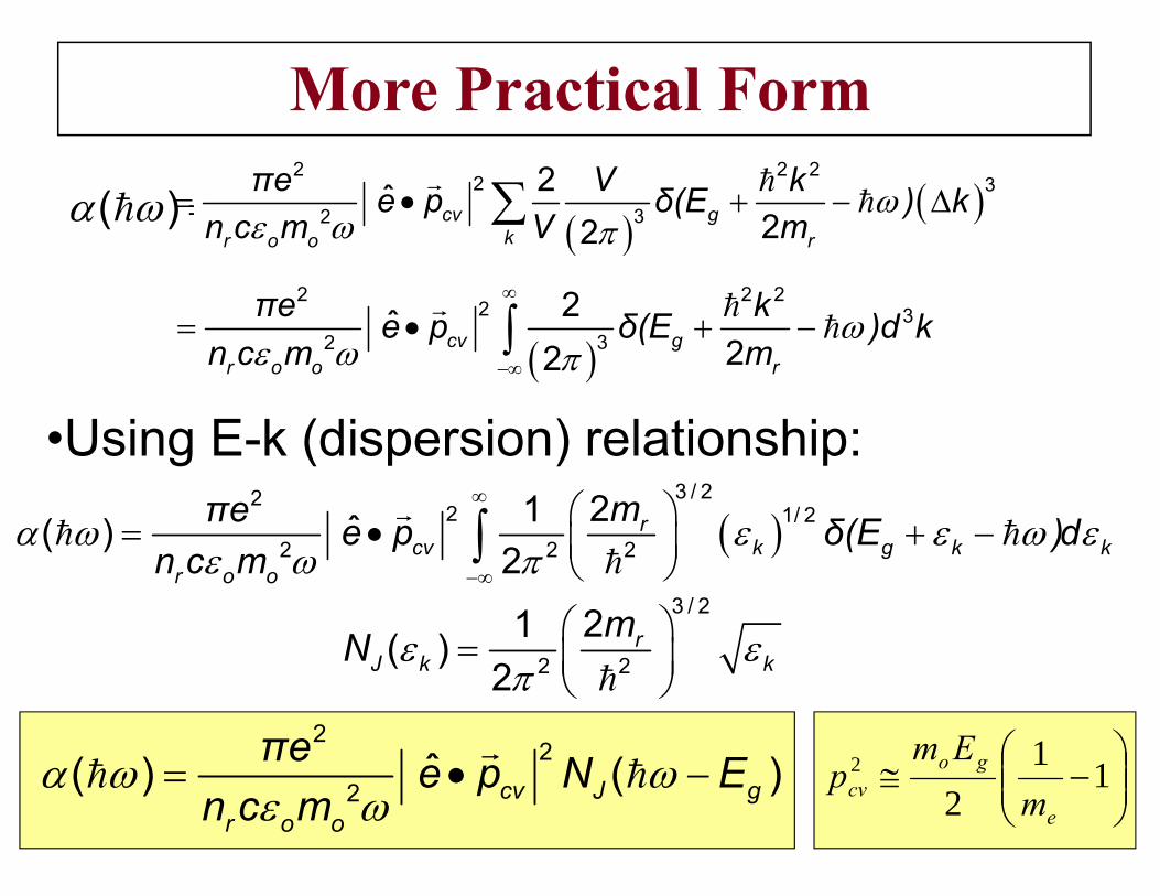
More Practical Form
22
2ˆ( ) ( )cv J g
r o o
πe e p N En c m
11
22
e
gocv m
Emp
2 2 22 3
32
2ˆ22
cv gkr o o r
πe V k e p δ(E ) kn c m V m
( )
2 2 22 3
32
2ˆ22
cv gr o o r
πe k e p δ(E )d kn c m m
3 / 22
2 1/ 22 2 2
21ˆ( )2
rcv k g k k
r o o
mπe e p δ(E )dn c m
•Using E-k (dispersion) relationship:
3 / 2
2 2
21( )2
rJ k k
mN

Conclusions
Yu, Cardona: p. 260
Absorption Coefficient at 5K
Red: calculation at 300K
•Example: InSb•Eg = 0.17eV
•Not 100% accurate•Parabolic band approximation•nr depends on wavelength•Exciton absorption below bandgap
•Different for 2D,1D,0D•Density of States


![Light absorption in hybrid silicon-on … absorption in hybrid silicon-on-insulator/quantum dot waveguides ... [2,3]. As a result, the ap-Published in: Optics Express · 2013Authors:](https://img.pdfslide.net/doc/110x75/5ac66fea7f8b9af91c8e2d6f/light-absorption-in-hybrid-silicon-on-absorption-in-hybrid-silicon-on-insulatorquantum.jpg)