Embed Size (px)
Citation preview
Microelectronics Reliability 38 (1998) 1705-1714
REVIEW PAPER
ESD FAILURE ANALYSIS METHODOLOGY
JIM COLVIN36217 Worthing Dr. Newark, CA 94560
Abstract-This paper reviews Failure Analysis methods and discusses the merits and pitfalls associated with some of the more common techniques as they relate toESD. Although advanced methods such as the Focused Ion Beam will be discussed, the importance of more traditional methods such as liquid crystal, emissionmicroscopy, passive voltage contrast and mechanical polishing will be emphasized. Case histories are based on ESD related failure analysis; however, many of thereferences cover general Failure Analysis methodology.
INTRODUCTION
Published papers for Failure Analysis date back to1954 for the Annual Symposium on Reliabilityand back to 1963 for the International ReliabilityPhysics Symposium (IRPS). Another familiarresource to the failure analyst in the USA is theSymposium for Testing and Failure Analysis(ISTFA). ISTFA proceedings were originallyknown as ATFA (Advanced Techniques inFailure Analysis) and date back to 1974. TheMicroelectronic Failure Analysis Desk Referenceis an important companion to the ISTFAWorkshops.IPFA (International Symposium on the Physicaland Failure Analysis of Integrated Circuits) isanother resource of information. The conferencefor IPFA has been held annually in Singapore forthe last 6 years. ESREF is a European forum forreliability of electron devices, failure physics andanalysis. ESREF held its first symposium in1990. Additional resources of information are theJournal of Electrostatics, an Elsevier publication,ESA (Electrostatics Society of America), and IEJ(Institute of Electrostatics Japan).The tools of the trade for the Failure Analystevolve constantly. Some tools such as theScanning Electron Microscope have endured thedecades, whereas other tools such as theultrasonic cutter were short lived due to the
advent of the laser cutter and subsequently theFocused Ion Beam. The tools of the modern labare a mixture of old and new. From the focusedion beam to mechanical polishing, each tool andtechnique has its place in the laboratory. Thereader is strongly encouraged to review thereferences for a thorough treatise on the coveredtopics.
CROSS CORRELATION
Before forging ahead into an analysis, it isimportant to understand what failure test data isrelevant. Resist the temptation to immediatelyjump on state of the art FA tools until the simplefacts have been gathered. A report that omitssupporting data and focuses on a single analyticalmethod will be perceived as a weak report. Themore exotic tools of FA must be used to reinforceor correlate the data for a sound corrective actionwhenever possible.Since the path of an analysis is unique for eachfailure, consider each analysis step carefullybefore proceeding, especially, when uniquefailures are involved. If the mechanism isrecurrent resulting in an abundance of samples,then cross-correlational methods are arequirement to a solid corrective action. Thereport the analyst generates must have sufficientsupporting data in numeric and or photographic
Microelectronics Reliability 38 (1998) 1705-1714
form to be believable to the reader. Since thewritten report is typically interpreted as theopinion of the analyst, document the data as alegal proof with sufficient supporting evidence.Try to generate the same damage on additionalparts in order to support a corrective action.Analyze different parts with the same problemusing multiple analytical methods. Arriving at thesame result using differing analytical paths suchas liquid crystal vs. Emission microscopy or cutand isolate techniques serves to reinforce theanalysis. Recreating the damage (Simulation)with either HBM or CDM methods helps toidentify whether the problem has more than oneroot cause. An example would be a poorlydesigned input protection scheme identified bydamage to the gate oxide of the protected input.This example combines a design weakness with aCDM issue on the test floor.Flowchart guides to failure analysis can be handyreferences, but lack the ability to teach commonsense. Beware the analyst that goes to a 1-weekcourse on electromigration and suddenly everyfailure mechanism encountered is due toelectromigration.
LIQUID CRYSTAL
Liquid crystal analysis techniques actually have arather lengthy history. Liquid crystal was firstused for failure analysis of dielectric integrity asearly as 1972 [1].The next step for LC was its ability to map logicstates of an operating IC somewhat similar tovoltage contrast methods in the SEM [2].Hot spot detection capabilities of liquid crystalwere known since 1967 but weren’t fully acceptedas a practical tool until the early 1980’s.Improved methods for cholesteric liquid crystalswere used for hot spot detection in 1981 [3].The current method of hot spot detection usingnematic liquid crystal involves using a crosspolarized microscope with K-18 liquid crystalfrom EM-Chemical Corp. Temperature controlclose to the transition point coupled with pulsed
power is required to maximize the sensitivity ofthis technique [4].Liquid crystal hot spot detection is commonlyused to locate leakage due to ESD events and isinexpensive. Some problems with liquid crystaltechniques pertaining to ESD analysis:1. The liquid crystal pools around wire bonds
and probe tips making identification of the hotspot difficult in some cases.
2. Temperature control fixturing adds overheadcost to the technique.
3. The number of layers between the source ofthe failure and the surface where the liquidcrystal resides limits spatial resolution andsensitivity.
4. Liquid crystal has a set transition temperature.Multiple hot spots can be difficult to resolve ifthe “warmer” spot creates a significanttemperature gradient.
FLUORESCENCE MICROTHERMALIMAGING (FMI)
FMI is a thermal detection technique similar toliquid crystal but is implemented in a similarfashion to emission microscopy. FMI uses a rareearth compound (EuTTA) europiumthenoyltrifluoroacteonate applied to the surface ofthe die in a similar manner as the application ofliquid crystal. The techniques differ in that FMIconverts the blackbody radiation of the sampleinto visible light (under ultraviolet excitation)which decreases with increasing temperature. Acomparison image is created from the die atambient by image subtraction of the unbiasedcondition from the biased condition. Localthermal differences appear due to the difference ingenerated visible light associated with the regionof interest. While the technique is an order ofmagnitude more sensitive than liquid crystal(.01C), it is also orders of magnitude moreexpensive to implement. FMI is a good techniquedue to both spatial resolution improvements andthermal detection improvements [5,6].
Microelectronics Reliability 38 (1998) 1705-1714
EMISSION MICROSCOPY
Emission Microscopy began as infrared emissionmicroscopy and was used originally to image nearinfrared energy emitted from CMOS latchup sites[7]. Since this technique images the light emittedfrom the latchup site, multiple latchup sites couldbe observed and the propagation of the effectcharacterized to enable debug. This method ofimaging was proven to be superior to liquidcrystal for latch up analysis due to the ability tospatially resolve multiple sites irrespective of atransition temperature.The next and rather significant step for emissionmicroscopy was directly related to ESDprotection structures. Using a transmission linepulse setup in conjunction with an infrared-viewing microscope allowed ESD related designto take a leap forward. A dynamic visualunderstanding of where the energy was going andhow it was being adsorbed for varying pulseenergies allowed models and rules to be createdfor ESD design [8,9]. An explanation of the non-uniform conduction in avalanche of an n-channeland subsequent weakness was derived comparedto a p-channel device as follows:1. Hot electrons are injected into the gate oxide
locally (positive drain voltage) associated withthe avalanche event. These hot electrons areresponsible for the reported “lock on” effectwhich generates a non-uniform region ofcurrent flow. The local trapping of theelectrons generates a local pinch-off in thechannel. The resulting high local electric fieldacts as a positive feedback effect, whichreduces the effectiveness of the n-channelprotection.
2. Conversely, the p-channel device reduces thelocal electric field (negative drain voltage) atthe avalanche site making the device stableand capable of dissipating much higherenergies.
Wider pulse widths (120 ns) were reported toresult in gate melting and contact spiking effects
due to localized heating of the silicon (secondbreakdown effects).As stated by the authors of this technique“EOS/ESD analysis will cease to be black magic,but will be transformed into a science.”Transmission line pulse methods are a commontool today coupled with emission microscopy [10-13].
EMISSION MICROSCOPY AND GATEOXIDE DAMAGE
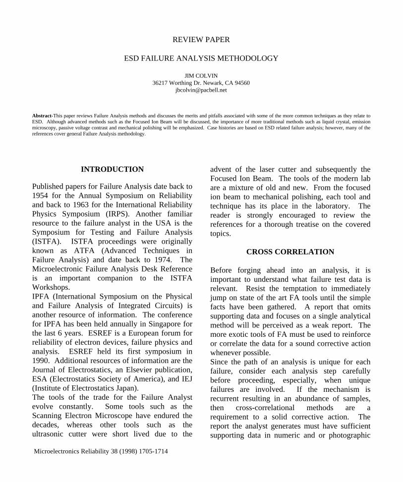
Emission microscopy of CDM created low levelgate leakage (Latent ESD) requires a considerableimprovement in emission microscopy [14,15].Once leakage has been identified associated withan input gate, the gate can be analyzed todetermine the number of leakage sites associatedwith that structure as well as the magnitude ofleakage at each site. Device geometry in thisexample was such that a major power buss waspositioned over a section of the input gate and theemission sites were located under the power buss.For this reason, the passivation surface wascracked gradually with a mechanical probe andmetal etch was used to remove the power bussover the input structure. The Focused Ion Beam(FIB) can also be used to open the buss. Theleakage of the input was confirmed to remainreasonably constant around the 100 nA range at5V.Emission microscopy was performed and twoemission sites associated with this one particularinput pin were identified. The bias voltage was10V. The reasons for this high bias voltage werethat no emission sites could be identified at lowervoltage ranges and this voltage value was prior toany permanent damage being done to the gate.The two emission sites had varying intensities asseen in figure 1.
Microelectronics Reliability 38 (1998) 1705-1714
Figure 1. Two emission locations were identified on the input gateresponsible for 110 nA of leakage at 5 Volts. The drive voltage was 10
volts with a CCD acquisition time of 400 seconds.
These emission sites correspond to the leakageassociated with each finger. This emission imagewas taken with a Zeiss Confocal Laser ScanningMicroscope and a CCD cooled camera. The CCDcooled camera was utilized with an integrationtime of approximately 400 seconds and noiseaveraged for this image to be observed. (Theseare extremely low-level emission sites). Mostintensified based emission microscopes, andcertainly the older infrared microscopes, areincapable of detecting such a low-level signatureof photon emission. This device was firstdeprocessed to expose the polycide and then eachpolycide finger was laser cut over field oxide tosever the individual fingers from the commonpolycide connection. The two edge fingers weremechanically probed and observed to leak,corresponding to the emission photograph (Figure1). Using a curve tracer set in DC mode at 5V,leakage on one finger was approximately 70nA,and 30nA on the other finger. Notice thiscorresponds roughly to the intensity of theemission sites from figure 1 and equals themeasured value of the leakage identified prior todeprocessing.
THE OPTICAL MICROSCOPE
Of all the tools available to the analyst, the opticalmicroscope is used routinely throughout theanalysis process. Optical microscopy has severalmodes of operation:1. Brightfield imaging uses light which is coaxial
through the objective and is the commonmode for imaging opaque surfaces.
2. Transmission mode is commonly used fortransparent specimens mounted on glassslides. This mode is commonly used forbiological specimens.
3. Darkfield imaging illuminates the sample atan angle. The resulting image revealselevated surface topography due to the scatterof light off of the edges of the elevatedsurface. This method is commonly used forsurface contaminant identification.
4. Interference contrast or Nomarski is used forthe identification of subtle surfacemorphology changes. Profile changes such asa thin film boundary are seen as a colorchange. Cross polarizers with a wedgeanalyzer are used in this mode.
5. Laser confocal microscopy allows 3Dreconstruction of surfaces for defect profiling.Laser based microscopes allow features to beidentified and characterized based on the laserwavelength.
6. Spinning disk confocal microscopes generatea similar effect to the interference contrastmode but with much greater depth of field andon entirely different principles. Objects,which are out of focus, are also attenuatedproportionately in brightness. Objects, whichare in focus, appear multicolored dependingupon the surface morphology.
Additional information on comparative data foroptical microscopy can be found in the suppliedreferences. [16-18]
Microelectronics Reliability 38 (1998) 1705-1714
THE SCANNING ELECTRONMICROSCOPE
The SEM has been a major part of failure analysislaboratories since the 1960’s. The SEM is used toimage as well as probe. Detectors associated witha SEM allow information to be gathered fromconductor potential to elemental analysis ofmaterials. Numerous probe methods haveevolved associated with the SEM [19-21].Secondary electron detection is the mostcommonly used mode for the SEM. This modeallows surface morphology to be ascertained dueto the high resolution coupled with a large depthof field. The SEM is a surface imaging tool andcannot image effectively through oxidescompared to an optical microscope. Electronbeam charging of insulators can be problematicand is typically addressed by using a fewnanometers of a sputtered conductive coating suchas carbon or gold. The references in this sectionprovide a thorough treatise on SEM techniques.
PASSIVE VOLTAGE CONTRAST
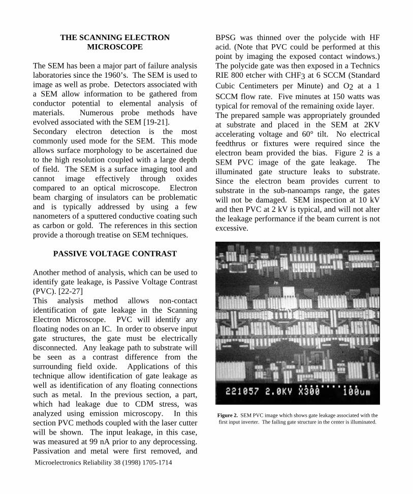
Another method of analysis, which can be used toidentify gate leakage, is Passive Voltage Contrast(PVC). [22-27]This analysis method allows non-contactidentification of gate leakage in the ScanningElectron Microscope. PVC will identify anyfloating nodes on an IC. In order to observe inputgate structures, the gate must be electricallydisconnected. Any leakage path to substrate willbe seen as a contrast difference from thesurrounding field oxide. Applications of thistechnique allow identification of gate leakage aswell as identification of any floating connectionssuch as metal. In the previous section, a part,which had leakage due to CDM stress, wasanalyzed using emission microscopy. In thissection PVC methods coupled with the laser cutterwill be shown. The input leakage, in this case,was measured at 99 nA prior to any deprocessing.Passivation and metal were first removed, and
BPSG was thinned over the polycide with HFacid. (Note that PVC could be performed at thispoint by imaging the exposed contact windows.)The polycide gate was then exposed in a TechnicsRIE 800 etcher with CHF3 at 6 SCCM (StandardCubic Centimeters per Minute) and O2 at a 1SCCM flow rate. Five minutes at 150 watts wastypical for removal of the remaining oxide layer.The prepared sample was appropriately groundedat substrate and placed in the SEM at 2KVaccelerating voltage and 60° tilt. No electricalfeedthrus or fixtures were required since theelectron beam provided the bias. Figure 2 is aSEM PVC image of the gate leakage. Theilluminated gate structure leaks to substrate.Since the electron beam provides current tosubstrate in the sub-nanoamps range, the gateswill not be damaged. SEM inspection at 10 kVand then PVC at 2 kV is typical, and will not alterthe leakage performance if the beam current is notexcessive.
Figure 2. SEM PVC image which shows gate leakage associated with thefirst input inverter. The failing gate structure in the center is illuminated.
Microelectronics Reliability 38 (1998) 1705-1714
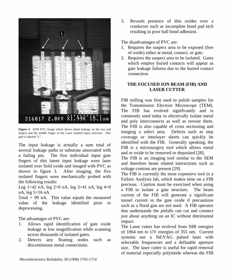
Figure 3. SEM PVC image which shows latent leakage on the two endfingers and the middle finger of the Laser isolated input structure. Thisgate is labeled "L".
The input leakage is actually a sum total ofseveral leakage paths to substrate associated witha failing pin. The five individual input gatefingers of this latent input leakage were laserisolated over field oxide and imaged with PVC asshown in figure 3. After imaging, the fiveisolated fingers were mechanically probed withthe following results:Leg 1=42 nA, leg 2=0 nA, leg 3=41 nA, leg 4=0nA, leg 5=16 nATotal = 99 nA. This value equals the measuredvalue of the leakage identified prior todeprocessing.
The advantages of PVC are:1. Allows rapid identification of gate oxide
leakage at low magnification while scanningacross thousands of isolated gates.
2. Detects any floating nodes such asdiscontinuous metal connections.
3. Reveals presence of thin oxides over aconductor such as incomplete bond pad etchresulting in poor ball bond adhesion.
The disadvantages of PVC are:1. Requires the suspect area to be exposed (free
of oxide) either at metal, contact, or gate.2. Requires the suspect area to be isolated. Gates
which employ buried contacts will appear asgate leakage failures due to the buried contactconnection.
THE FOCUSED ION BEAM (FIB) ANDLASER CUTTER
FIB milling was first used to polish samples forthe Transmission Electron Microscope (TEM).The FIB has evolved significantly and iscommonly used today to electrically isolate metaland poly interconnects as well as reroute them.The FIB is also capable of cross sectioning andimaging a select area. Defects such as stepcoverage or interlayer shorts can quickly beidentified with the FIB. Generally speaking, theFIB is a microsurgery tool which allows metaland or oxide to be removed or deposited [28].The FIB is an imaging tool similar to the SEMand therefore beam related interactions such asvoltage contrast are present [29].The FIB is currently the most expensive tool in aFailure Analysis lab, which makes time on a FIBprecious. Caution must be exercised when usinga FIB to isolate a gate structure. The beamcurrent of the FIB will generate a significanttunnel current in the gate oxide if precautionssuch as a flood gun are not used. A FIB operatorthat understands the pitfalls can cut and connectjust about anything on an IC without detrimentalimpact.The Laser cutter has evolved from NIR energiesof 1064 nm to UV energies of 355 nm. Currentsystems use a Nd:YAG pulsed laser withselectable frequencies and a definable aperturesize. The laser cutter is useful for rapid removalof material especially polyimide whereas the FIB
Microelectronics Reliability 38 (1998) 1705-1714
is not great at removal of polyimide. Windows inpassivation can be opened where nitride materialsare involved and metallization can be vapordeposited with a laser [30]. The laser is faster butnot as precise or repeatable as the FIB. Beamcharging effects are not an issue with the lasercutter making it a good choice for in situ cut andisolate techniques.
DELAYERING ANDSTAIN ENHANCEMENT
Delineation of layers or defects dates back to1955 when W.C. Dash developed what is knownas Dash etch today. Dash etch is a HF-HNO3
system currently used for p-n junction delineation.Other etchants such as Sirtl etch are based on aHF-CrO3 system. Sirtl etch delineates defects suchas stacking faults and dislocations in silicon. Sirtletch has excellent wetting properties and workswell as a poly etch for revealing dielectricintegrity issues in the MOSFET channel. Wrightetch is an improved version of Sirtl etch withnitric acid and copper nitrate combined in the HF-HNO3 system. Wright etch is commonly used fordamage enhancement in ESD analysis. There arecurrently thirty-eight additional etch formulationswhich should not be ignored. An excellentresource for etch delineation as well asdeprocessing recipes and references was recentlypublished by T.W. Lee in 1996 [31].
SURFACE LAPPING TECHNIQUES
Sample preparation is straightforward and a fewguidelines will result in repeatable clean results.Use high selectivity etches such as KOH or CsOHto insure an endpoint on the point of interest.Other etches include 49% HF, or metal etchants.Etches which are not highly selective such as apoly etch containing nitric and HF, will not leavecrisp definition associated with silicon to oxideboundary and will, in many cases, remove toomuch gate oxide. Mechanical surface lappingtechniques allow layers to be partially exposed and
then removed using a selective etch. In order toexpose the gate oxide of a failing transistor toexamine the gate oxide integrity topographically,the following procedure is employed:
A. Surface polish the part using 1 micron diamondmylar lapping film or if planarity needs to bemaintained use a napless cloth with colloidal silicasuch as chem-pol on an orbital polisher. Once theoxides over poly 2 are eliminated, use HCl toremove the silicide then heated KOH to removethe exposed poly surface. Endpoint is determinedempirically. The etch will endpoint on the gateoxide with a 200:1 selectivity and remove anysilicon radially under the defect. High oxidesidewalls will be seen which may interfere withimaging in the Atomic Force Microscope AFMdue to tip convolution. The sample can at thispoint be stripped of oxide using HF and thesubstrate or poly 1 cells imaged as desired.Surface lapping eliminates etch undercut andartifacts common with traditional delayering andis useful for AFM as well as SEM imaging.
SELECTING THE RIGHT TOOL FOR THEANALYSIS OF ESD FAILURES
As a general guideline, emission microscopy is apoor choice when dealing with ohmic leakagesuch as ESD damage to a contact or junction.Typically most of the energy liberated is bestdetected using a thermal detection technique suchas liquid crystal or fluorescence microthermalimaging (FMI). Emission microscopy is usuallythe best choice when dealing with damaged gateoxides or junction related phenomena. Sincetransmission pulse methods result in amps ofcurrent flowing through the protection structuresin a repetitive mode, it is clear that sensitivity isless an issue where design verification isinvolved. All emission tools of today, be theyCCD based or intensified systems, offer orders ofmagnitude sensitivity gain over the original IRimaging methods which used an S-1 photocathode(Gain = 10X).Cut and isolate methods to isolate leakage can beperformed with the laser cutter, FIB, or by
Microelectronics Reliability 38 (1998) 1705-1714
mechanical probe. Caution needs to be exercisedwhere fragile gate oxides are involved due topossible beam charging in the FIB.
THE FUTURE OF ESD FAILUREANALYSIS
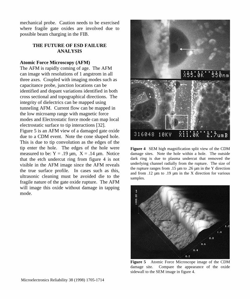
Atomic Force Microscopy (AFM)The AFM is rapidly coming of age. The AFMcan image with resolutions of 1 angstrom in allthree axes. Coupled with imaging modes such ascapacitance probe, junction locations can beidentified and dopant variations identified in bothcross sectional and topographical directions. Theintegrity of dielectrics can be mapped usingtunneling AFM. Current flow can be mapped inthe low microamp range with magnetic forcemodes and Electrostatic force mode can map localelectrostatic surface to tip interactions [32].Figure 5 is an AFM view of a damaged gate oxidedue to a CDM event. Note the cone shaped hole.This is due to tip convolution as the edges of thetip enter the hole. The edges of the hole weremeasured to be: Y = .19 µm, X = .14 µm. Noticethat the etch undercut ring from figure 4 is notvisible in the AFM image since the AFM revealsthe true surface profile. In cases such as this,ultrasonic cleaning must be avoided die to thefragile nature of the gate oxide rupture. The AFMwill image this oxide without damage in tappingmode.
Figure 4 SEM high magnification split view of the CDMdamage sites. Note the hole within a hole. The outsidedark ring is due to plasma undercut that removed theunderlying channel radially from the rupture. The size ofthe rupture ranges from .15 µm to .26 µm in the Y directionand from .12 µm to .19 µm in the X direction for varioussamples.
Figure 5 Atomic Force Microscope image of the CDMdamage site. Compare the appearance of the oxidesidewall to the SEM image in figure 4.
Microelectronics Reliability 38 (1998) 1705-1714
Backside Emission Microscopy
Backside Emission Microscopy is rapidlybecoming popular and could be used withtransmission line pulsing techniques, however, theeffects of thinning the substrate must be takeninto account.Backside emission microscopy simply refers toperforming emission microscopy imaged from thepolished and thinned substrate of the device [33-40]. Backside emission is used due to the numberof metal layers blocking a clear view from above. There are several significant challengesassociated with backside emission microscopy:
1. Sample preparation methods.2. Thinning the substrate will impact device
characteristics. The device will have reducedthermal and electrical conduction transportcharacteristics and an increase in the parasiticgain for latchup where low ohmic substratesare involved.
3. Silicon is an infrared filter and limitsdetection bandwidth of emission sites.
4. Dopants in the silicon serve to scatter NIRenergy resulting in attenuation of sensitivity.
5. CCD based systems have a low quantumefficiency in the required NIR spectrum.
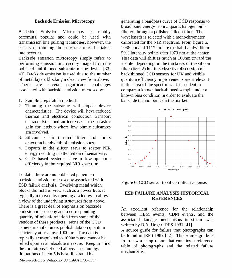
To date, there are no published papers onbackside emission microscopy associated withESD failure analysis. Overlying metal whichblocks the field of view such as a power buss istypically removed by opening a window to allowa view of the underlying structures from above.There is a great deal of emphasis on backsideemission microscopy and a correspondingquantity of misinformation from some of thevendors of these products. None of the CCDcamera manufacturers publish data on quantumefficiency at or above 1000nm. The data istypically extrapolated to 1000nm and cannot berelied upon as an absolute measure. Keep in mindthe limitations 1-4 cited above. Technologylimitations of item 5 is best illustrated by
generating a bandpass curve of CCD response tobroad band energy from a quartz halogen bulbfiltered through a polished silicon filter. Thewavelength is selected with a monochromatorcalibrated for the NIR spectrum. From figure 6,1036 nm and 1117 nm are the half bandwidth or50% intensity points with 1073 nm at the center.This data will shift as much as 100nm toward thevisible depending on the thickness of the siliconfilter (item 2) but it is clear that discussion ofback thinned CCD sensors for UV and visiblequantum efficiency improvements are irrelevantin this area of the spectrum. It is prudent tocompare a known back-thinned sample under aknown bias condition in order to evaluate thebackside technologies on the market.
S i f i l t e r t o C C D B a n d p a s s
W a v e l e n g t h
0
0.1
0.2
0.3
0.4
0.5
0.6
0.7
0.8
0.9
1
980 1000 1020 1040 1060 1080 1100 1120 1140 1160 1180
Figure 6. CCD sensor to silicon filter response.
ESD FAILURE ANALYSIS HISTORICALREFERENCES
An excellent reference for the relationshipbetween HBM events, CDM events, and theassociated damage mechanisms in silicon waswritten by B.A. Unger IRPS 1981 [41].A source guide for failure trait photographs canbe found in IRPS 1982 [42]. This source guide isfrom a workshop report that contains a referencetable of photographs and the related failuremechanisms.
Microelectronics Reliability 38 (1998) 1705-1714
A discussion on thermal runaway commonlyknown as second breakdown can be found inISTFA 1984 by Middendorf and Hausken [43].This paper covers the following failuremechanisms: Junction damage, gate oxidedamage, poly filaments, aluminum melt filamentsand fused open conductors.A study of CDM failures for input and outputstructures for two different designs can be foundin EOS/ESD 1994 by N. Maene et al. [44].J. Never and S. Voldman used the AFM inconjunction with the SEM to show subtledifferences in surface morphology after secondbreakdown damage in EOS/ESD 1995 [45].
REFERENCES
1. “Spotting IC Pinholes with Liquid Crystals,”Electronics, Vol. 45, No. 5, p.136, February 28, 1972.
2. “D.J. Channin, “Liquid-Crystal Technique forObserving Integrated Circuit Operation,” IEEETransactions on Electron Devices, Oct 1974, pgs. 650-652.
3. John Hiatt, “A Method of Detecting Hot Spots onSemiconductors Using Liquid Crystals,” IRPS 1981,pp. 130-133.
4. D. Burgess et al., “Improved Sensitivity for Hot SpotDetection Using Liquid Crystals,” IRPS 1984. pp119-127.
5. D.L. Barton, “Fluorescent MicrothermographicImaging,” ISTFA 1994, pp.87-95.
6. V.J. Bruce, “Comparison of FluorescentMicrothermography to Other Commercially AvailableTechniques,” ISTFA 1994, pp. 73-80.
7. “Pulsed Infra-Red Microscopy for Debugging Latch-Up on CMOS Products,” IEEE IRPS 1984 pp122-127.
8. N. Khurana, T. Maloney, W. Yeh, “ESD in CHMOSDevices - Equivalent Circuits, Physical Models andFailure Mechanisms”, in Proc. IRPS Symp., 1985, pp.212-223.
9. T. J. Maloney, N. Khurana, “Transmission LinePulsing Techniques for Circuit Modeling of ESDPhenomena”, in Proc. EOS/ESD Symp., 1985, pp. 49-54.
10. C. Russ et al, “Non-Uniform Triggering of gg-nMOStInvestigated by Combined Emission Microscopy andTransmission Line Pulsing”, in Proc. EOS/ESD Symp.,1998. Pp. unknown.
11. M. Cavone et al, “A Method for the Characterizationand Evaluation of ESD Protection Structures andNetworks”, in Proc. EOS/ESD Symp., 1994, pp. 292-300.
12. A. Amerasekera et al., “An Analysis of Low VoltageESD Damage in Advanced CMOS Processes,” 1990EOS/ESD Symposium Proceedings, EOS-12, pp. 143-150.
13. P. Salome et al.,”Study of a 3D Phenomenon DuringESD Stresses in Deep Submicron CMOS TechnologiesUsing Photon Emission Tool,”IEEE-35th ReliabilityPhysics Symposium, 1997, pp. 325-332.
14. J. Colvin, “The Identification and Analysis of LatentESD Damage on CMOS Input Gates,” 1993 EOS/ESDSymposium Proceedings, EOS-15, pp. 109-116.
15. B. Bossmann, et al., “Failure Analysis Techniqueswith the Confocal Laser Scanning Microscope”,ISTFA/92 Proceedings, pp. 351-361.
16. Kevin P. Hussey, Stewart L. Selesky, "Laser ScanMicroscopy Applications for Microelectronic FailureAnalysis," Proc. ISTFA, pp. 259-265, 1990.
17. T.W. Joseph, et al., "Infrared Laser Microscopy ofStructures on Heavily Doped Silicon," Proc. ISTFA,pp. 1-7, 1992.
18. B. Bossmann, et al., “Failure Analysis Techniqueswith the Confocal Laser Scanning Microscope”,ISTFA/92 Proceedings, pp. 351-361.
19. J.R. Beall, “Voltage Contrast Techniques andProcedures,” Microelectronic Failure Analysis DeskReference, 3rd edition. Pp 153-161.
20. E.I. Cole and J.M. Soden, “Scanning ElectronMicroscopy Techniques for IC Failure Analysis,”Microelectronic Failure Analysis Desk Reference, 3rd
edition. Pp 163-175.21. J. Colvin, “A New Technique to Rapidly Identify Low
Level Gate Oxide Leakage In Field EffectSemiconductors Using a Scanning ElectronMicroscope”, 1990 EOS/ESD SymposiumProceedings, EOS-12, pp. 173-176.
22. IBID.23. J. Colvin, “A New Technique to Rapidly Identify Gate
Oxide Leakage In Field Effect Semiconductors Usinga Scanning Electron Microscope”, 1990 ISTFASymposium Proceedings, pp. 331-336.
24. J. Colvin, “The Identification and Analysis of LatentESD Damage on CMOS Input Gates,” 1993 EOS/ESDSymposium Proceedings, EOS-15, pp. 109-116.
25. T.J. Aton et al. “Using Scanned Electron Beams forTesting Microstructure Isolation and Continuity,”IRPS 1991 pp239-244.
26. E.I. Cole and J.M. Soden, “Scanning ElectronMicroscopy Techniques for IC Failure Analysis,”
Microelectronics Reliability 38 (1998) 1705-1714
Microelectronic Failure Analysis Desk Reference, 3rd
edition. Pp 170-171.27. Leo G. Henry,”Failure Analysis of CMOS PALS
Exhibiting ESD-type Polygate Short To Substrateusing a State-of-the-Art IC Diagnostic uProberSystem,” 1994 EOS/ESD Symposium Proceedings,EOS-16, pp. 324-334.
28. K.S. Wills, “Microsurgery Technology for IntegratedCircuits,” ISTFA 1997 Microelectronics WorkshopDesk Reference Addendum pp. 264-295.
29. A.N. Campbell et al, “Electrical Biasing and VoltageContrast Imaging in a Focused Ion Beam System,”ISTFA 1995 pp. 33-41.
30. K.S. Wills, “Microsurgery Technology for IntegratedCircuits,” ISTFA 1997 Microelectronics WorkshopDesk Reference Addendum pp. 282-295.
31. T.W. Lee, “A Review of Wet Etch Formulas forSilicon Semiconductor Failure Analysis,” ISTFA 1996pp. 319-331.
32. Y. Strausser, J. Colvin “Atomic Force Microscopy:Modes and Analytical Techniques with the ScanningProbe Microscope,” Microelectronic Failure AnalysisDesk Reference, 4th edition ASM International.
33. B. Picart and G. Deboy, "Failure Analysis on VLSICircuits Using Emission Microscopy for BacksideObservation," Proc. ESREF, pp. 515-520, 1992.
34. K. Etoh, "Infrared Emission Microscope AnalyzesDefects in Multilevel LSI and Silicon Bulk," NikkeiElectronics Asia, pp. 66-69, Sept. 1992.
35. E. Inuzuka,et al, "Emission Analysis of SemiconductorDevices from Backside of the Chip," Proc. ESREF, pp.269-272, 1992.
36. T. Ishii,et al., "Functional Failure AnalysisTechnology from Backside of VLSI Chip," Proc.ISTFA, pp. 41-47, 1994.
37. K. Naitoh,et al., "Investigation of MultiLevelMetallization ULSIs by Light Emission from the Back-Side and Front-Side of the Chip," Proc. ISTFA, pp.145-151, 1997.
38. T. W. Joseph, et al., "Infrared Laser Microscopy ofStructures on Heavily Doped Silicon," Proc. ISTFA,pp. 1-7, 1992.
39. N. M. Wu, et al., "Failure Analysis from Back Side ofDie," Proc. ISTFA, pp.393-399, 1996.
40. D. L. Barton, et al., "Infrared Light Emission fromSemiconductor Devices," Proc. ISTFA, pp. 9-17,1996.
41. Unger, B.A. “Electrostatic Failures of SemiconductorDevices,” IEEE-19th Reliability Physics Symposium,1981, pp. 193-199.
42. R.C. Walker et al, “Workshop Report, EOS/ESDDamage Failure Trait Photograph Interpretation,”
IEEE-20th Reliability Physics Symposium, 1982, pp.278-283.
43. M.J. Middendorf et al., “Observed Physical Effectsand Failure Analysis of EOS/ESD on MOS Devices,”ISTFA 1984, pp.205-213.
44. N.Maene et al., “Failure Analysis of CDM Failures ina Mixed Analog/Digital Circuit,” 1994 EOS/ESDSymposium Proceedings, EOS-16, pp. 307-314.
45. J.N. Never and S.H. Voldman,”Failure Analysis ofShallow Trench Isolated ESD Structures,” 1995EOS/ESD Symposium Proceedings, EOS-17, pp. 273-288.
ADDITIONAL REFERENCES
46. Doyle, E., W. Morris “RADC Microelectronics FailureAnalysis Procedural Guide” Reliability AnalysisCenter(RAC), Catalogue No. MFAT-1.
47. McAteer, O.J., R.E. Twist “Analysis of ElectrostaticDischarge Failures,” IITRI-EOS/ESD Symposium,Sept. 1981, RAC Catalogue No.EOS-3, pp. 14-20.
48. Koyler, J.M., W.E. Anderson “Selection of PackagingMaterials For Electrostatic Discharge-Sensitive (ESD)Items,” ibid, pp. 75-84.
49. Enders, J. “Susceptibility of IC’s in ElectrostaticDamage Step-Stress Test,” ibid, pp. 106-113.\
50. Clark, O.M. “Lighning Protection For Computer DataLines,” ibid, pp. 212-218.
51. Chase, E.W. “Evaluation of Electrostatic (ESD)Damage To 16K EPROMS,” ibid, pp. 236-241.
52. Bossard, P.R., R.G. Chemelli, B.A. Unger “ESDDamage from Triboelectrically Charged IC Pins,”IITRI-EOS/ESD Symposium, Sept. 1980, RAC Cata-logue NO. EOS-2, pp. 17-22.
53. Hart, A. R., T. Teng “LSI Design Consideration forESD Protection Structures Related to Process andLayout Variations,” ibid, pp. 87-94.
54. Turner, T.E., S. Morris “Electrostatic Sensitivity ofVarious Input Protection Networks,” ibid, pp. 95-103.
55. Schwank, i.R., R.P. Baker, M.G. Armendariz“Surprising Patterns of MOS Susceptibvility to ESDand Implications on Long Term Reliability,” ibid, pp.104-111.
56. Anand, Y., G. Morris, V. Higgins “ElectrostaticFailure on X-Band Silicon Schottky Barrier Diodes,”ibid, pp. 97-103.
57. Teng, T.T., A.R. Hart, A. McKenna “Susceptibility ofLSI MOS to Electrostatic Discharge at ElevatedTemperature,” ibid, pp. 168-175
58. Soden, J. M. “The Dielectric Strength of SiliconDioxide in a CMOS Transistor Structure,” ibid, pp.176-182.
Microelectronics Reliability 38 (1998) 1705-1714
59. Smith, J.S. “High Current Transient Induced JunctionShorts,” IEEE-9th Reliability Physics Symposium,1971, pp. 163-171.
60. Speakman, T.S. “A Model for the Failure of BipolarSilicon Integrated Circuits Subjected to ElectrostaticDischarge,” IEEE-12th Reliability Physics Symposium,1974, pp. 60-69.
61. Gajda, J.J. “Techniques in Failure Analysis of MOSDevices,” ibid, pp. 30-37.
62. Freeman, E.R., J.R. Beall “Control of ElectrostaticDischarge Damage to Semiconductors,” ibid, pp.304-312.
63. Beall, J.R., L. Hamiter “EBIC - A Valuable Tool forSemiconductor Evaluation and Failure Analysis,”IEEE-15th Reliability Physics Symposium, 1977, pp.61-69.
64. Minear, R.L., G.A. Dodson “Effects of ElectrostaticDischarge on Linear Bipolar Integrated Circuits,” ibid,pp. 138-143.
65. Yang, D.Y., W.C. Johnson, M.A. Lampert “A Study ofthe Dielectric Breakdown of Thermally Grown SiliconDioxide by the Self-Quenching Technique,” IEEE-13th
Reliability Physics Symposium, 1975, pp. 10-14.66. Fisch, D.E. “A New Technique for Input Protection
Testing,” IEEE-19th Reliability Physics Symposium,1981, pp. 212-217.
67. Lytle, W.J., O.J. McAteer “Characteristic Traits ofSemiconductor Failures,” IEEE-Proceedings, 1970Annual Symposium on Reliability, pp. 386-393.
68. McAteer, O.J. “Electrostatic Damage in HYBRIDAssemblies,” 1978 Reliability and MaintainabilitySymposium, 9 pp.
69. Trigonis, A.C. “Electrostatic Discharge inMicrocircuits Detection and Protection Techniques,”Annual Reliability and Maintainability Symposium,Contract No. NAS 7-100, Jan. 18, 1975.
70. Smith, J.S. “Pulse Power Testing of Microcircuits,”Rept. No. RADC-TR-71-59, Oct. 1979.
71. Domingos, H. “Electro-Thermal Overstress Failure inMicreelectronics,” Rept. No. RADC-TR-73-87 April1973.
72. Whelan, C.D. “Reliability Evaluation of C/MOSTechnology in Complex Integrated Circuits,” Rept.No. RADC-TR-C-0282, March 1976, 210 pp.
73. ICE/RADC, “Microcircuit Manufacturing ControlHandbook” Integrated Circuit Engineering.
74. Shumka, A., E.L. Miller, R.R. Piety “Failure Modesand Analysis Techniques for CMOS Microcircuits,”IEEE-Advanced Techniques in Failure AnalysisSymposium, 1977, pp. 75-87.
75. Riga, G. “Failure Analysis , Feedback to IntegratedCircuits Design and Fabrication,” IEEE-Advanced
Techniques in Failure Analysis Symposium, 1977, pp.99-103.