Embed Size (px)
Citation preview
JWBS064-fm JWBS064-Gerbennikov March 15, 2011 22:29 Printer Name: Yet to Come
RF AND MICROWAVETRANSMITTER DESIGN
Andrei GrebennikovBell Labs, Alcatel-Lucent, Ireland
A JOHN WILEY & SONS, INC., PUBLICATION
iii

JWBS064-fm JWBS064-Gerbennikov March 15, 2011 22:29 Printer Name: Yet to Come

JWBS064-fm JWBS064-Gerbennikov March 15, 2011 22:29 Printer Name: Yet to Come
RF AND MICROWAVETRANSMITTER DESIGN
i

JWBS064-fm JWBS064-Gerbennikov March 15, 2011 22:29 Printer Name: Yet to Come
WILEY SERIES IN MICROWAVE AND OPTICAL ENGINEERING
KAI CHANG, EditorTexas A&M University
A complete list of the titles in this series appears at the end of this volume.
ii

JWBS064-fm JWBS064-Gerbennikov March 15, 2011 22:29 Printer Name: Yet to Come
RF AND MICROWAVETRANSMITTER DESIGN
Andrei GrebennikovBell Labs, Alcatel-Lucent, Ireland
A JOHN WILEY & SONS, INC., PUBLICATION
iii

JWBS064-fm JWBS064-Gerbennikov March 15, 2011 22:29 Printer Name: Yet to Come
Copyright C© 2011 by John Wiley & Sons, Inc. All rights reserved.
Published by John Wiley & Sons, Inc., Hoboken, New Jersey.Published simultaneously in Canada.
No part of this publication may be reproduced, stored in a retrieval system, or transmitted in any form or by any means,electronic, mechanical, photocopying, recording, scanning, or otherwise, except as permitted under Section 107 or 108 of the1976 United States Copyright Act, without either the prior written permission of the Publisher, or authorization through paymentof the appropriate per-copy fee to the Copyright Clearance Center, Inc., 222 Rosewood Drive, Danvers, MA 01923,(978) 750-8400, fax (978) 750-4470, or on the web at www.copyright.com. Requests to the Publisher for permissionshould be addressed to the Permissions Department, John Wiley & Sons, Inc., 111 River Street, Hoboken, NJ 07030,(201) 748-6011, fax (201) 748-6008, or online at http://www.wiley.com/go/permission.
Limit of Liability/Disclaimer of Warranty: While the publisher and author have used their best efforts in preparing this book,they make no representations or warranties with respect to the accuracy or completeness of the contents of this book andspecifically disclaim any implied warranties of merchantability or fitness for a particular purpose. No warranty may be created orextended by sales representatives or written sales materials. The advice and strategies contained herein may not be suitable foryour situation. You should consult with a professional where appropriate. Neither the publisher nor author shall be liable for anyloss of profit or any other commercial damages, including but not limited to special, incidental, consequential, or other damages.
For general information on our other products and services or for technical support, please contact our Customer CareDepartment within the United States at (800) 762-2974, outside the United States at(317) 572-3993 or fax (317) 572-4002.
Wiley also publishes its books in a variety of electronic formats. Some content that appears in print may not be available inelectronic formats. For more information about Wiley products, visit our web site at www.wiley.com
Library of Congress Cataloging-in-Publication Data:
Grebennikov, AndreiRF and microwave transmitter design/Andrei Grebennikov.
p. cm.Includes bibliographical references and index.ISBN 978-0-470-52099-4 (cloth)
Printed in Singapore
oBook ISBN: 978-0-470-92930-8ePDF ISBN: 978-0-470-92929-1
10 9 8 7 6 5 4 3 2 1
iv
JWBS064-fm JWBS064-Gerbennikov March 15, 2011 11:32 Printer Name: Yet to Come
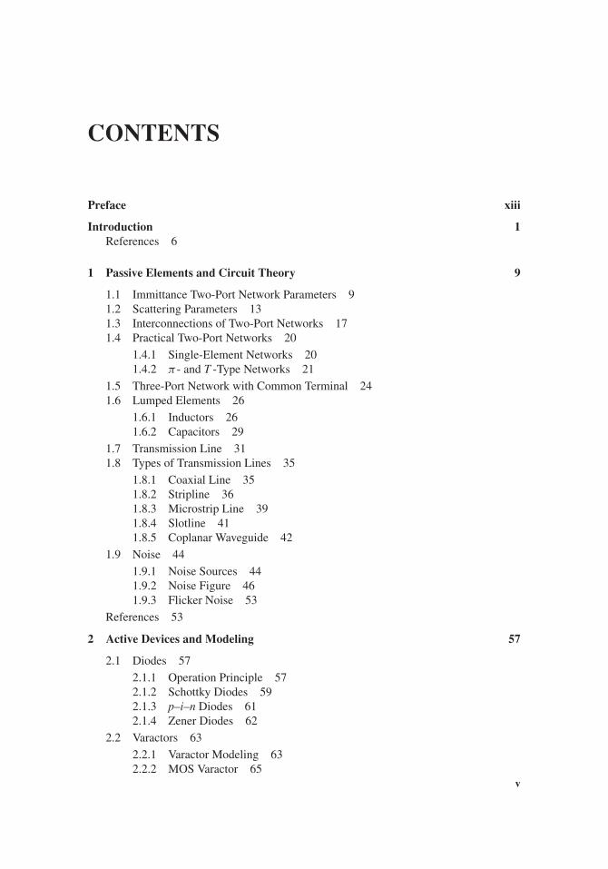
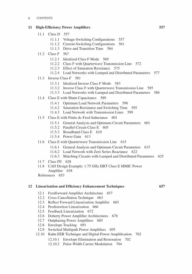
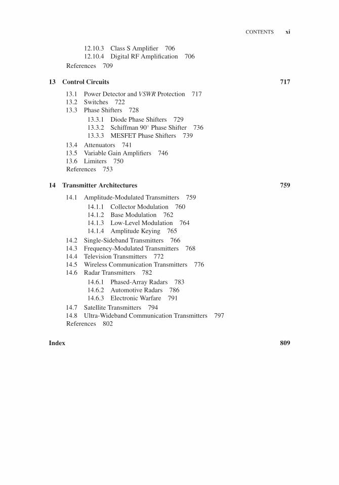
CONTENTS
Preface xiii
Introduction 1References 6
1 Passive Elements and Circuit Theory 9
1.1 Immittance Two-Port Network Parameters 91.2 Scattering Parameters 131.3 Interconnections of Two-Port Networks 171.4 Practical Two-Port Networks 20
1.4.1 Single-Element Networks 201.4.2 π - and T -Type Networks 21
1.5 Three-Port Network with Common Terminal 241.6 Lumped Elements 26
1.6.1 Inductors 261.6.2 Capacitors 29
1.7 Transmission Line 311.8 Types of Transmission Lines 35
1.8.1 Coaxial Line 351.8.2 Stripline 361.8.3 Microstrip Line 391.8.4 Slotline 411.8.5 Coplanar Waveguide 42
1.9 Noise 44
1.9.1 Noise Sources 441.9.2 Noise Figure 461.9.3 Flicker Noise 53
References 53
2 Active Devices and Modeling 57
2.1 Diodes 57
2.1.1 Operation Principle 572.1.2 Schottky Diodes 592.1.3 p–i–n Diodes 612.1.4 Zener Diodes 62
2.2 Varactors 63
2.2.1 Varactor Modeling 632.2.2 MOS Varactor 65
v
JWBS064-fm JWBS064-Gerbennikov March 15, 2011 11:32 Printer Name: Yet to Come
vi CONTENTS
2.3 MOSFETs 70
2.3.1 Small-Signal Equivalent Circuit 702.3.2 Nonlinear I–V Models 732.3.3 Nonlinear C–V Models 752.3.4 Charge Conservation 782.3.5 Gate–Source Resistance 792.3.6 Temperature Dependence 792.3.7 Noise Model 81
2.4 MESFETs and HEMTs 83
2.4.1 Small-Signal Equivalent Circuit 832.4.2 Determination of Equivalent Circuit Elements 852.4.3 Curtice Quadratic Nonlinear Model 882.4.4 Parker–Skellern Nonlinear Model 892.4.5 Chalmers (Angelov) Nonlinear Model 912.4.6 IAF (Berroth) Nonlinear Model 932.4.7 Noise Model 94
2.5 BJTs and HBTs 97
2.5.1 Small-Signal Equivalent Circuit 972.5.2 Determination of Equivalent Circuit Elements 982.5.3 Equivalence of Intrinsic π - and T -Type Topologies 1002.5.4 Nonlinear Bipolar Device Modeling 1022.5.5 Noise Model 105
References 107
3 Impedance Matching 113
3.1 Main Principles 1133.2 Smith Chart 1163.3 Matching with Lumped Elements 120
3.3.1 Analytic Design Technique 1203.3.2 Bipolar UHF Power Amplifier 1313.3.3 MOSFET VHF High-Power Amplifier 135
3.4 Matching with Transmission Lines 138
3.4.1 Analytic Design Technique 1383.4.2 Equivalence Between Circuits with Lumped and Distributed
Parameters 1443.4.3 Narrowband Microwave Power Amplifier 1473.4.4 Broadband UHF High-Power Amplifier 149
3.5 Matching Networks with Mixed Lumped and Distributed Elements 151References 153
4 Power Transformers, Combiners, and Couplers 155
4.1 Basic Properties 155
4.1.1 Three-Port Networks 1554.1.2 Four-Port Networks 156
4.2 Transmission-Line Transformers and Combiners 158
JWBS064-fm JWBS064-Gerbennikov March 15, 2011 11:32 Printer Name: Yet to Come
CONTENTS vii
4.3 Baluns 1684.4 Wilkinson Power Dividers/Combiners 1744.5 Microwave Hybrids 1824.6 Coupled-Line Directional Couplers 192References 197
5 Filters 201
5.1 Types of Filters 2015.2 Filter Design Using Image Parameter Method 205
5.2.1 Constant-k Filter Sections 2055.2.2 m-Derived Filter Sections 207
5.3 Filter Design Using Insertion Loss Method 210
5.3.1 Maximally Flat Low-Pass Filter 2105.3.2 Equal-Ripple Low-Pass Filter 2135.3.3 Elliptic Function Low-Pass Filter 2165.3.4 Maximally Flat Group-Delay Low-Pass Filter 219
5.4 Bandpass and Bandstop Transformation 2225.5 Transmission-Line Low-Pass Filter Implementation 225
5.5.1 Richards’s Transformation 2255.5.2 Kuroda Identities 2265.5.3 Design Example 228
5.6 Coupled-Line Filters 228
5.6.1 Impedance and Admittance Inverters 2285.6.2 Coupled-Line Section 2315.6.3 Parallel-Coupled Bandpass Filters Using Half-Wavelength
Resonators 2345.6.4 Interdigital, Combline, and Hairpin Bandpass Filters 2365.6.5 Microstrip Filters with Unequal Phase Velocities 2395.6.6 Bandpass and Bandstop Filters Using Quarter-Wavelength
Resonators 241
5.7 SAW and BAW Filters 243References 250
6 Modulation and Modulators 255
6.1 Amplitude Modulation 255
6.1.1 Basic Principle 2556.1.2 Amplitude Modulators 259
6.2 Single-Sideband Modulation 262
6.2.1 Double-Sideband Modulation 2626.2.2 Single-Sideband Generation 2656.2.3 Single-Sideband Modulator 266
6.3 Frequency Modulation 267
6.3.1 Basic Principle 2686.3.2 Frequency Modulators 273
6.4 Phase Modulation 278
JWBS064-fm JWBS064-Gerbennikov March 15, 2011 11:32 Printer Name: Yet to Come
viii CONTENTS
6.5 Digital Modulation 283
6.5.1 Amplitude Shift Keying 2846.5.2 Frequency Shift Keying 2876.5.3 Phase Shift Keying 2896.5.4 Minimum Shift Keying 2966.5.5 Quadrature Amplitude Modulation 2996.5.6 Pulse Code Modulation 300
6.6 Class-S Modulator 3026.7 Multiple Access Techniques 304
6.7.1 Time and Frequency Division Multiplexing 3046.7.2 Frequency Division Multiple Access 3056.7.3 Time Division Multiple Access 3056.7.4 Code Division Multiple Access 306
References 308
7 Mixers and Multipliers 311
7.1 Basic Theory 3117.2 Single-Diode Mixers 3137.3 Balanced Diode Mixers 318
7.3.1 Single-Balanced Mixers 3187.3.2 Double-Balanced Mixers 321
7.4 Transistor Mixers 3267.5 Dual-Gate FET Mixer 3297.6 Balanced Transistor Mixers 331
7.6.1 Single-Balanced Mixers 3317.6.2 Double-Balanced Mixers 334
7.7 Frequency Multipliers 338References 344
8 Oscillators 347
8.1 Oscillator Operation Principles 347
8.1.1 Steady-State Operation Mode 3478.1.2 Start-Up Conditions 349
8.2 Oscillator Configurations and Historical Aspect 3538.3 Self-Bias Condition 3588.4 Parallel Feedback Oscillator 3628.5 Series Feedback Oscillator 3658.6 Push–Push Oscillators 3688.7 Stability of Self-Oscillations 3728.8 Optimum Design Techniques 376
8.8.1 Empirical Approach 3768.8.2 Analytic Approach 379
8.9 Noise in Oscillators 385
8.9.1 Parallel Feedback Oscillator 386
JWBS064-fm JWBS064-Gerbennikov March 15, 2011 11:32 Printer Name: Yet to Come
CONTENTS ix
8.9.2 Negative Resistance Oscillator 3928.9.3 Colpitts Oscillator 3948.9.4 Impulse Response Model 397
8.10 Voltage-Controlled Oscillators 4078.11 Crystal Oscillators 4178.12 Dielectric Resonator Oscillators 423References 428
9 Phase-Locked Loops 433
9.1 Basic Loop Structure 4339.2 Analog Phase-Locked Loops 4359.3 Charge-Pump Phase-Locked Loops 4399.4 Digital Phase-Locked Loops 4419.5 Loop Components 444
9.5.1 Phase Detector 4449.5.2 Loop Filter 4499.5.3 Frequency Divider 4549.5.4 Voltage-Controlled Oscillator 457
9.6 Loop Parameters 461
9.6.1 Lock Range 4619.6.2 Stability 4629.6.3 Transient Response 4639.6.4 Noise 465
9.7 Phase Modulation Using Phase-Locked Loops 4669.8 Frequency Synthesizers 469
9.8.1 Direct Analog Synthesizers 4699.8.2 Integer-N Synthesizers Using PLL 4699.8.3 Fractional-N Synthesizers Using PLL 4719.8.4 Direct Digital Synthesizers 473
References 474
10 Power Amplifier Design Fundamentals 477
10.1 Power Gain and Stability 47710.2 Basic Classes of Operation: A, AB, B, and C 48710.3 Linearity 49610.4 Nonlinear Effect of Collector Capacitance 50310.5 DC Biasing 50610.6 Push–Pull Power Amplifiers 51510.7 Broadband Power Amplifiers 52210.8 Distributed Power Amplifiers 53710.9 Harmonic Tuning Using Load–Pull Techniques 543
10.10 Thermal Characteristics 549References 552
JWBS064-fm JWBS064-Gerbennikov March 15, 2011 11:32 Printer Name: Yet to Come
x CONTENTS
11 High-Efficiency Power Amplifiers 557
11.1 Class D 557
11.1.1 Voltage-Switching Configurations 55711.1.2 Current-Switching Configurations 56111.1.3 Drive and Transition Time 564
11.2 Class F 567
11.2.1 Idealized Class F Mode 56911.2.2 Class F with Quarterwave Transmission Line 57211.2.3 Effect of Saturation Resistance 57511.2.4 Load Networks with Lumped and Distributed Parameters 577
11.3 Inverse Class F 581
11.3.1 Idealized Inverse Class F Mode 58311.3.2 Inverse Class F with Quarterwave Transmission Line 58511.3.3 Load Networks with Lumped and Distributed Parameters 586
11.4 Class E with Shunt Capacitance 589
11.4.1 Optimum Load Network Parameters 59011.4.2 Saturation Resistance and Switching Time 59511.4.3 Load Network with Transmission Lines 599
11.5 Class E with Finite dc-Feed Inductance 601
11.5.1 General Analysis and Optimum Circuit Parameters 60111.5.2 Parallel-Circuit Class E 60511.5.3 Broadband Class E 61011.5.4 Power Gain 613
11.6 Class E with Quarterwave Transmission Line 615
11.6.1 General Analysis and Optimum Circuit Parameters 61511.6.2 Load Network with Zero Series Reactance 62211.6.3 Matching Circuits with Lumped and Distributed Parameters 625
11.7 Class FE 62811.8 CAD Design Example: 1.75 GHz HBT Class E MMIC Power
Amplifier 638References 653
12 Linearization and Efficiency Enhancement Techniques 657
12.1 Feedforward Amplifier Architecture 65712.2 Cross Cancellation Technique 66312.3 Reflect Forward Linearization Amplifier 66512.4 Predistortion Linearization 66612.5 Feedback Linearization 67212.6 Doherty Power Amplifier Architectures 67812.7 Outphasing Power Amplifiers 68512.8 Envelope Tracking 69112.9 Switched Multipath Power Amplifiers 695
12.10 Kahn EER Technique and Digital Power Amplification 702
12.10.1 Envelope Elimination and Restoration 70212.10.2 Pulse-Width Carrier Modulation 704
JWBS064-fm JWBS064-Gerbennikov March 15, 2011 11:32 Printer Name: Yet to Come
CONTENTS xi
12.10.3 Class S Amplifier 70612.10.4 Digital RF Amplification 706
References 709
13 Control Circuits 717
13.1 Power Detector and VSWR Protection 71713.2 Switches 72213.3 Phase Shifters 728
13.3.1 Diode Phase Shifters 72913.3.2 Schiffman 90◦ Phase Shifter 73613.3.3 MESFET Phase Shifters 739
13.4 Attenuators 74113.5 Variable Gain Amplifiers 74613.6 Limiters 750References 753
14 Transmitter Architectures 759
14.1 Amplitude-Modulated Transmitters 759
14.1.1 Collector Modulation 76014.1.2 Base Modulation 76214.1.3 Low-Level Modulation 76414.1.4 Amplitude Keying 765
14.2 Single-Sideband Transmitters 76614.3 Frequency-Modulated Transmitters 76814.4 Television Transmitters 77214.5 Wireless Communication Transmitters 77614.6 Radar Transmitters 782
14.6.1 Phased-Array Radars 78314.6.2 Automotive Radars 78614.6.3 Electronic Warfare 791
14.7 Satellite Transmitters 79414.8 Ultra-Wideband Communication Transmitters 797References 802
Index 809

JWBS064-fm JWBS064-Gerbennikov March 15, 2011 11:32 Printer Name: Yet to Come
xii
JWBS064-fm JWBS064-Gerbennikov March 15, 2011 11:32 Printer Name: Yet to Come
PREFACE
The main objective of this book is to present all relevant information required to design the transmit-ters in general and their main components in particular in different RF and microwave applicationsincluding well-known historical and recent novel architectures, theoretical approaches, circuit simu-lation results, and practical implementation techniques. This comprehensive book can be very usefulfor lecturing to promote the systematic way of thinking with analytical calculations and practicalverification, thus making a bridge between theory and practice of RF and microwave engineering.As a result, this book is intended for and can be recommended to university-level professors as acomprehensive material to help in lecturing for graduate and postgraduate students, to researchersand scientists to combine the theoretical analysis with practical design and to provide a sufficientbasis for innovative ideas and circuit design techniques, and to practicing designers and engineers asthe book contains numerous well-known and novel practical circuits, architectures, and theoreticalapproaches with detailed description of their operational principles and applications.
Chapter 1 introduces the basic two-port networks describing the behavior of linear and nonlinearcircuits. To characterize the nonlinear properties of the bipolar or field-effect transistors, their equiv-alent circuit elements are expressed through the impedance Z -parameters, admittance Y -parameters,or hybrid H -parameters. On the other hand, the transmission ABCD-parameters are very importantfor the design of the distributed circuits such as a transmission line or cascaded elements, whereasthe scattering S-parameters are widely used to simplify the measurement procedure. The design for-mulas and curves are given for several types of transmission lines including stripline, microstrip line,slotline, and coplanar waveguide. Monolithic implementation of lumped inductors and capacitors isusually required at microwave frequencies and for portable devices. Knowledge of noise phenomenasuch as noise figure, additive white noise, low-frequency fluctuations, or flicker noise in active orpassive elements is very important for the oscillator modeling in particular and entire transmitterdesign in general.
In Chapter 2, all necessary steps to provide an accurate device modeling procedure starting withthe determination of the device small-signal equivalent circuit parameters are described and discussed.A variety of nonlinear models for MOSFET, MESFET, HEMT, and BJT devices including HBTs,which are very prospective for modern microwave monolithic integrated circuits, are given. In orderto highlight the advantages or drawbacks of one over another nonlinear device model, a comparisonof the measured and modeled volt–ampere and voltage–capacitance characteristics, as well as afrequency range of model application, are analyzed.
The main principles and impedance matching tools are described in Chapter 3. Generally, anoptimum solution depends on the circuit requirements, such as the simplicity in practical realization,frequency bandwidth and minimum power ripple, design implementation and adjustability, stableoperation conditions, and sufficient harmonic suppression. As a result, many types of the matchingnetworks are available, including lumped elements and transmission lines. To simplify and visualizethe matching design procedure, an analytical approach, which allows calculation of the parameters ofthe matching circuits using simple equations, and Smith chart traces are discussed. In addition, severalexamples of the narrowband and broadband power amplifiers using bipolar or MOSFET devices aregiven, including successive and detailed design considerations and explanations.
Chapter 4 describes the basic properties of the three-port and four-port networks, as well as avariety of different combiners, transformers, and directional couplers for RF and microwave power
xiii
JWBS064-fm JWBS064-Gerbennikov March 15, 2011 11:32 Printer Name: Yet to Come
xiv PREFACE
applications. For power combining in view of insufficient power performance of the active devices, itis best to use the coaxial-cable combiners with ferrite core to combine the output powers of RF poweramplifiers intended for wideband applications. Since the device output impedance is usually too smallfor high power level, to match this impedance with a standard 50-� load, it is necessary to use thecoaxial-line transformers with specified impedance transformation. For narrowband applications, theN -way Wilkinson combiners are widely used due to the simplicity of their practical realization. Atthe same time, the size of the combiners should be very small at microwave frequencies. Therefore,the commonly used hybrid microstrip combiners including different types of the microwave hybridsand directional couplers are described and analyzed.
Chapter 5 introduces the basic types of RF and microwave filters based on the low-pass or high-pass sections and bandpass or bandstop transformation. Classical filter design approaches using imageparameter and insertion loss methods are given for low-pass and high-pass LC filter implementa-tions. The quarterwave-line and coupled-line sections, which are the basic elements of microwavetransmission-line filters, are described and analyzed. Different examples of coupled-line filters in-cluding interdigital, combline, and hairpin bandpass filters are given. Special attention is paid tomicrostrip filters with unequal phase velocities, which can provide unexpected properties becauseof different implementation technologies. Finally, the typical structures, implementation technology,operational principles, and band performance of the filters based on surface and bulk acoustic wavesare presented.
Chapter 6 discusses the basic features of different types of analog modulation including amplitude,single-sideband, frequency, and phase modulation, and basic types of digital modulation such asamplitude shift keying, frequency shift keying, phase shift keying, or pulse code modulation andtheir variations. The principle of operations and various schematics of the modulators for differentmodulation schemes including Class S modulator for pulse-width modulation are described. Finally,the concept of time and frequency division multiplexing is introduced, as well as a brief descriptionof different multiple access techniques.
A basic theory describing the operational principles of frequency conversion in receivers andtransmitters is given in Chapter 7. The different types of mixers, from the simplest based on a singlediode to a balanced and double-balanced type based on both diodes and transistors, are described andanalyzed. The special case is a mixer based on a dual-gate transistor that provides better isolationbetween signal paths and simple implementation. The frequency multipliers that historically were avery important part of the vacuum-tube transmitters can extend the operating frequency range.
Chapter 8 presents the principles of oscillator design, including start-up and steady-state opera-tion conditions, noise and stability of oscillations, basic oscillator configurations using lumped andtransmission-line elements, and simplified equation-based oscillator analyses and optimum designtechniques. An immittance design approach is introduced and applied to the series and parallel feed-back oscillators, including circuit design and simulation aspects. Voltage-controlled oscillators andtheir varactor tuning range and linearity for different oscillator configurations are discussed. Finally,the basic circuits and operation principles of crystal and dielectric resonator oscillators are given.
Chapter 9 begins with description of the basic phase-locked loop concept. Then, the basic perfor-mance and structures of the analog, charge-pump, and digital phase-locked loops are analyzed. Thebasic loop components such as phase detector, loop filter, frequency divider, and voltage-controlledoscillator are discussed, as well as loop dynamic parameters. The possibility and particular realiza-tions of the phase modulation using phase-locked loops are presented. Finally, general classes offrequency synthesizer techniques such as direct analog synthesis, indirect synthesis, and direct digitalsynthesis are discussed. The proper choice of the synthesizer type is based on the number of fre-quencies, frequency spacing, frequency switching time, noise, spurious level, particular technology,and cost.
Chapter 10 introduces the fundamentals of the power amplifier design, which is generally a com-plicated procedure when it is necessary to provide simultaneously accurate active device modeling,effective impedance matching depending on the technical requirements and operation conditions,stability in operation, and simplicity in practical implementation. The quality of the power amplifier
JWBS064-fm JWBS064-Gerbennikov March 15, 2011 11:32 Printer Name: Yet to Come
PREFACE xv
design is evaluated by realized maximum power gain under stable operation condition with minimumamplifier stages, and the requirement of linearity or high efficiency can be considered where it isneeded. For a stable operation, it is necessary to evaluate the operating frequency domains where theactive device may be potentially unstable. To avoid the parasitic oscillations, the stabilization circuittechnique for different frequency domains (from low frequencies up to high frequencies close to thedevice transition frequency) is discussed. The key parameter of the power amplifier is its linearity,which is very important for many wireless communication applications. The relationships betweenthe output power, 1-dB gain compression point, third-order intercept point, and intermodulation dis-tortions of the third and higher orders are given and illustrated for different active devices. The devicebias conditions, which are generally different for linearity or efficiency improvement, depend on thepower amplifier operation class and the type of the active device. The basic Classes A, AB, B, and Cof the power amplifier operation are introduced, analyzed, and illustrated. The principles and designof the push–pull amplifiers using balanced transistors, as well as broadband and distributed poweramplifiers, are discussed. Harmonic-control techniques for designing microwave power amplifiersare given with description of a systematic procedure of multiharmonic load–pull simulation using theharmonic balance method and active load–pull measurement system. Finally, the concept of thermalresistance is introduced and heatsink design issues are discussed.
Modern commercial and military communication systems require the high-efficiency long-termoperating conditions. Chapter 11 describes in detail the possible circuit solutions to provide a high-efficiency power amplifier operation based on using Class D, Class F, Class E, or their newlydeveloped subclasses depending on the technical requirements. In all cases, an efficiency improvementin practical implementation is achieved by providing the nonlinear operation conditions when anactive device can simultaneously operate in pinch-off, active, and saturation regions, resulting innonsinusoidal collector current and voltage waveforms, symmetrical for Class D and Class F andasymmetrical for Class E (DE, FE) operation modes. In Class F amplifiers analyzed in frequencydomain, the fundamental-frequency and harmonic load impedances are optimized by short-circuittermination and open-circuit peaking to control the voltage and current waveforms at the deviceoutput to obtain maximum efficiency. In Class E amplifiers analyzed in time domain, an efficiencyimprovement is achieved by realizing the on/off active device switching operation (the pinch-off andsaturation modes) with special current and voltage waveforms so that high voltage and high currentdo not concur at the same time.
In modern wireless communication systems, it is very important to realize both high-efficiencyand linear operation of the power amplifiers. Chapter 12 describes a variety of techniques andapproaches that can improve the power amplifier performance. To increase efficiency over powerbackoff range, the Doherty, outphasing, and envelope-tracking power amplifier architectures, as wellas switched multipath power amplifier configurations, are discussed and analyzed. There are severallinearization techniques that provide linearization of both entire transmitter system and individualpower amplifier. Feedforward, cross cancellation, or reflect forward linearization techniques areavailable technologies for satellite and cellular base station applications achieving very high linearitylevels. The practical realization of these techniques is quite complicated and very sensitive to boththe feedback loop imbalance and the parameters of its individual components. Analog predistortionlinearization technique is the simplest form of power amplifier linearization and can be used forhandset application, although significant linearity improvement is difficult to realize. Different typesof the feedback linearization approaches, together with digital linearization techniques, are veryattractive to be used in handset or base station transmitters. Finally, the potential semidigital anddigital amplification approaches are discussed with their architectural advantages and problems inpractical implementation.
Chapter 13 discusses the circuit schematics and main properties of the semiconductor controlcircuits that are usually characterized by small size, low power consumption, high-speed performance,and operating life. Generally, they can be built based on the p–i–n diodes, silicon MOSFET, or GaAsMESFET transistors and can be divided into two basic parts: amplitude and phase control circuits.The control circuits are necessary to protect high power devices from excessive peak voltage or

JWBS064-fm JWBS064-Gerbennikov March 15, 2011 11:32 Printer Name: Yet to Come
xvi PREFACE
dc current conditions. They are also used as switching elements for directing signal between differenttransmitting paths, as variable gain amplifiers to stabilize transmitter output power, as attenuators andphase shifters to change the amplitude and phase of the transmitting signal paths in array systems, oras limiters to protect power-sensitive components.
Finally, Chapter 14 describes the different types of radio transmitter architectures, history of radiocommunication, conventional types of radio transmission, and modern communication systems.Amplitude-modulated transmitters representing the oldest technique for radio communication arebased on high- or low-level modulation methods, with particular case of an amplitude keying.Single-sideband transmitters as the next-generation transmitters could provide higher efficiency dueto the transmission of a single sideband only. Frequency-modulated transmitters then became arevolutionary step to improve the quality of a broadcast transmission. TV transmitters include differentmodulation techniques for transmitting audio and video information, both analog and digital. Wirelesscommunication transmitters as a part of the cellular technologies provide a worldwide wireless radioaccess. Radar transmitters are required for many commercial and military applications such asphased-array radars, automotive radars, or electronic warfare systems. Satellite transmission systemscontribute to worldwide transmission of any communication signals through satellite transponders andoffer communication for areas with any population density and location. Ultra-wideband transmissionis very attractive for their low-cost and low-power communication applications, occupying a verywide frequency range.
ACKNOWLEDGMENTS
To Drs. Frederick Raab and Lin Fujiang for useful comments and suggestions in book organizationand content covering.
To Dr. Frank Mullany from Bell Labs, Ireland, for encouragement and support.The author especially wishes to thank his wife, Galina Grebennikova, for performing computer-
artwork design, as well as for her constant support, inspiration, and assistance.
Andrei Grebennikov
JWBS064-cintro JWBS064-Gerbennikov March 11, 2011 19:44 Printer Name: Yet to Come
INTRODUCTION
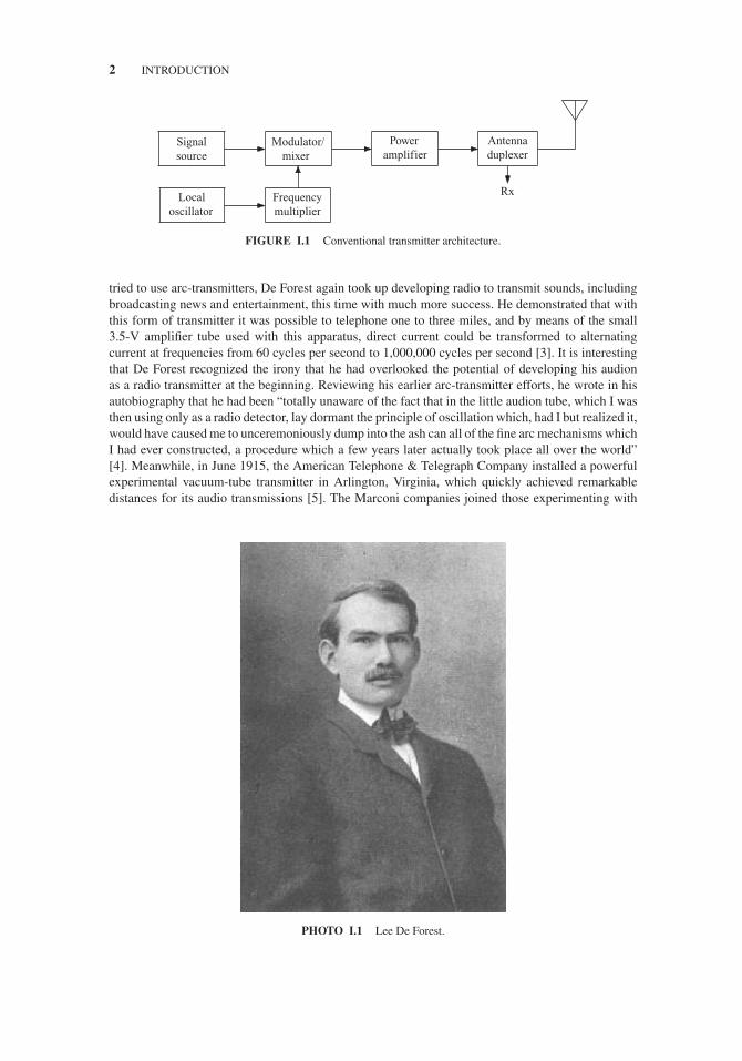
A vacuum-tube or solid-state radio transmitter is essentially a source of a radio-frequency (RF)signal to be transmitted through antenna in different radio systems such as wireless communication,television (TV) and broadcasting, navigation, radar, or satellite, the information format and electricalperformance of which should satisfy the corresponding standard requirements. The transmissionof radio signals is produced by modulation of different types, with different output power andtransmission mode, and in different frequency ranges, from high frequencies to millimeter waves.Transmitters in which the power output is generated directly by the modulated source are consideredas possessing high-level modulation systems. In contrast, arrangements in which the modulation takesplace at a power level less than the transmitter output are referred to as low-level modulation systems.
Figure I.1 shows the simplified block diagram of a conventional radio transmitter intended tooperate at radio and microwave frequencies, which consists of the following: the source of theinformation signal, which is usually amplified, filtered, or transformed to the intermediate frequency;the local oscillator and frequency multiplier, which establish the stabilized carrier frequency orsome multiple of it; the RF modulator or mixer, which combines the signal and carrier frequencycomponents to produce one of the varieties of the RF modulated waves; the power amplifier to deliverthe RF modulated signal of required power level to the antenna; the antenna duplexer to separateand isolate transmitting and receiving paths. The power amplifier usually consists of cascaded gainstages, and each stage should have adequate linearity in the case of transmitting signal with variableamplitude corresponding to amplitude-modulated or multicarrier signals. In practice, there are manyvariations in transmitter architectures depending on the particular frequency bandwidth, output power,or modulation scheme.
Dr. Lee De Forest was an inventor who changed the world with electronics by inventing thevacuum tube, which he called the audion. In January 1907, De Forest filed a patent for an oscillationdetector based on a three-electrode device representing a vacuum tube [1]. His pioneering innovationwas the insertion of a third electrode (grid) in between the cathode (filament) and the anode (plate) ofthe previously invented diode. However, it was not until 1911 that De Forest built the first vacuum-tube amplifier based on three audions as amplifiers [2]. The original audion was capable of slightlyamplifying received signals, but at this stage could not be used for more advanced applications such asradio transmitters. The inefficient design of the original audion meant that it was initially of little valueto radio, and due to its high cost and short life it was rarely used. Eventually, vacuum-tube design wasimproved enough to make vacuum tubes more than novelties. Beginning in 1912, various researchersdiscovered that properly constructed (i.e., according to scientific and engineering principles) vacuumtubes could be employed in electrical circuits that made radio receivers and amplifiers thousands oftimes more powerful, and could also be used to make compact and efficient radio transmitters, whichfor the first time made radio broadcasting practical.
In 1914, the first vacuum-tube radio transmitters began to appear—a key technical developmentthat would lead to the introduction of widespread broadcasting. Both amateurs and commercial firmsstarted to experiment with the new vacuum-tube transmitters, employing them for a variety of pur-poses. Six years after suspending his efforts to make audio transmissions, when he had unsuccessfully
RF and Microwave Transmitter Design, First Edition. Andrei Grebennikov.C© 2011 John Wiley & Sons, Inc. Published 2011 by John Wiley & Sons, Inc.
1
JWBS064-cintro JWBS064-Gerbennikov March 11, 2011 19:44 Printer Name: Yet to Come
2 INTRODUCTION
Poweramplifier
Antennaduplexer
RxFrequencymultiplier
Localoscillator
Signalsource
Modulator/mixer
FIGURE I.1 Conventional transmitter architecture.
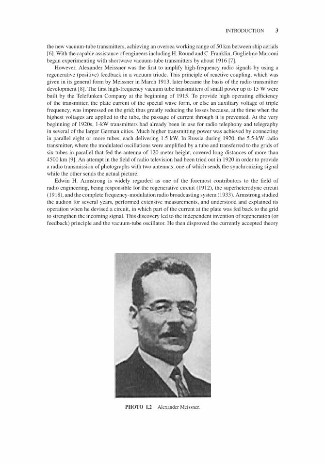
tried to use arc-transmitters, De Forest again took up developing radio to transmit sounds, includingbroadcasting news and entertainment, this time with much more success. He demonstrated that withthis form of transmitter it was possible to telephone one to three miles, and by means of the small3.5-V amplifier tube used with this apparatus, direct current could be transformed to alternatingcurrent at frequencies from 60 cycles per second to 1,000,000 cycles per second [3]. It is interestingthat De Forest recognized the irony that he had overlooked the potential of developing his audionas a radio transmitter at the beginning. Reviewing his earlier arc-transmitter efforts, he wrote in hisautobiography that he had been “totally unaware of the fact that in the little audion tube, which I wasthen using only as a radio detector, lay dormant the principle of oscillation which, had I but realized it,would have caused me to unceremoniously dump into the ash can all of the fine arc mechanisms whichI had ever constructed, a procedure which a few years later actually took place all over the world”[4]. Meanwhile, in June 1915, the American Telephone & Telegraph Company installed a powerfulexperimental vacuum-tube transmitter in Arlington, Virginia, which quickly achieved remarkabledistances for its audio transmissions [5]. The Marconi companies joined those experimenting with
PHOTO I.1 Lee De Forest.
JWBS064-cintro JWBS064-Gerbennikov March 11, 2011 19:44 Printer Name: Yet to Come
INTRODUCTION 3
the new vacuum-tube transmitters, achieving an oversea working range of 50 km between ship aerials[6]. With the capable assistance of engineers including H. Round and C. Franklin, Guglielmo Marconibegan experimenting with shortwave vacuum-tube transmitters by about 1916 [7].
However, Alexander Meissner was the first to amplify high-frequency radio signals by using aregenerative (positive) feedback in a vacuum triode. This principle of reactive coupling, which wasgiven in its general form by Meissner in March 1913, later became the basis of the radio transmitterdevelopment [8]. The first high-frequency vacuum tube transmitters of small power up to 15 W werebuilt by the Telefunken Company at the beginning of 1915. To provide high operating efficiencyof the transmitter, the plate current of the special wave form, or else an auxiliary voltage of triplefrequency, was impressed on the grid; thus greatly reducing the losses because, at the time when thehighest voltages are applied to the tube, the passage of current through it is prevented. At the verybeginning of 1920s, 1-kW transmitters had already been in use for radio telephony and telegraphyin several of the larger German cities. Much higher transmitting power was achieved by connectingin parallel eight or more tubes, each delivering 1.5 kW. In Russia during 1920, the 5.5-kW radiotransmitter, where the modulated oscillations were amplified by a tube and transferred to the grids ofsix tubes in parallel that fed the antenna of 120-meter height, covered long distances of more than4500 km [9]. An attempt in the field of radio television had been tried out in 1920 in order to providea radio transmission of photographs with two antennas: one of which sends the synchronizing signalwhile the other sends the actual picture.
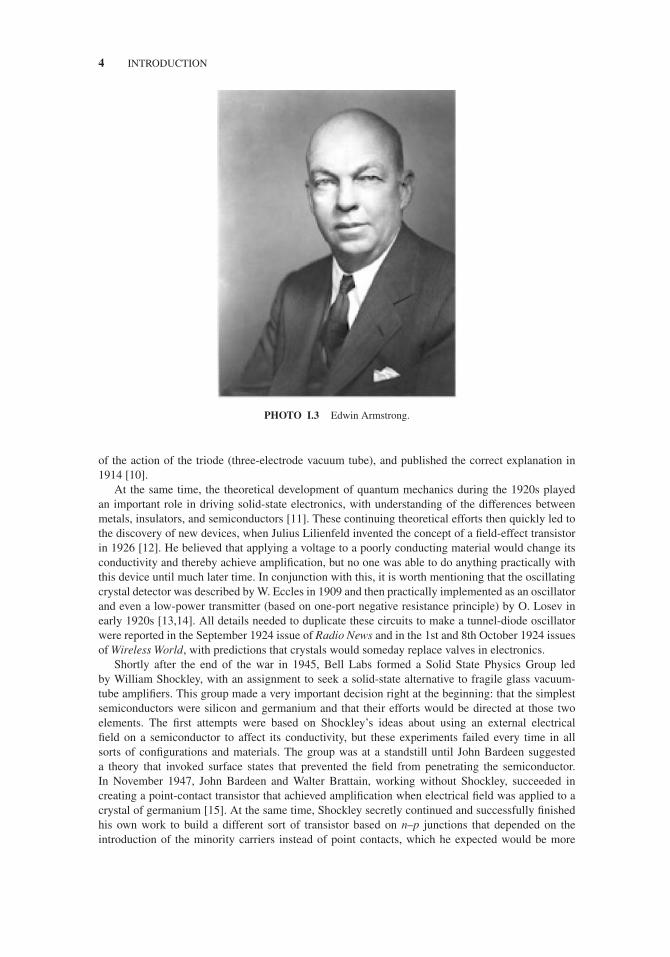
Edwin H. Armstrong is widely regarded as one of the foremost contributors to the field ofradio engineering, being responsible for the regenerative circuit (1912), the superheterodyne circuit(1918), and the complete frequency-modulation radio broadcasting system (1933). Armstrong studiedthe audion for several years, performed extensive measurements, and understood and explained itsoperation when he devised a circuit, in which part of the current at the plate was fed back to the gridto strengthen the incoming signal. This discovery led to the independent invention of regeneration (orfeedback) principle and the vacuum-tube oscillator. He then disproved the currently accepted theory
PHOTO I.2 Alexander Meissner.
JWBS064-cintro JWBS064-Gerbennikov March 11, 2011 19:44 Printer Name: Yet to Come
4 INTRODUCTION
PHOTO I.3 Edwin Armstrong.
of the action of the triode (three-electrode vacuum tube), and published the correct explanation in1914 [10].
At the same time, the theoretical development of quantum mechanics during the 1920s playedan important role in driving solid-state electronics, with understanding of the differences betweenmetals, insulators, and semiconductors [11]. These continuing theoretical efforts then quickly led tothe discovery of new devices, when Julius Lilienfeld invented the concept of a field-effect transistorin 1926 [12]. He believed that applying a voltage to a poorly conducting material would change itsconductivity and thereby achieve amplification, but no one was able to do anything practically withthis device until much later time. In conjunction with this, it is worth mentioning that the oscillatingcrystal detector was described by W. Eccles in 1909 and then practically implemented as an oscillatorand even a low-power transmitter (based on one-port negative resistance principle) by O. Losev inearly 1920s [13,14]. All details needed to duplicate these circuits to make a tunnel-diode oscillatorwere reported in the September 1924 issue of Radio News and in the 1st and 8th October 1924 issuesof Wireless World, with predictions that crystals would someday replace valves in electronics.
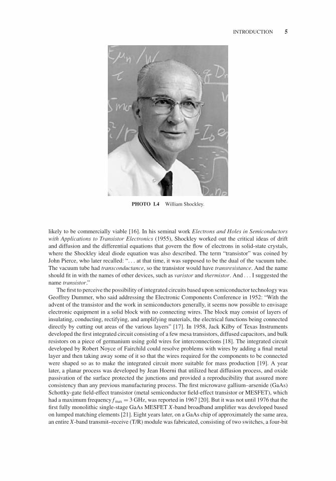
Shortly after the end of the war in 1945, Bell Labs formed a Solid State Physics Group ledby William Shockley, with an assignment to seek a solid-state alternative to fragile glass vacuum-tube amplifiers. This group made a very important decision right at the beginning: that the simplestsemiconductors were silicon and germanium and that their efforts would be directed at those twoelements. The first attempts were based on Shockley’s ideas about using an external electricalfield on a semiconductor to affect its conductivity, but these experiments failed every time in allsorts of configurations and materials. The group was at a standstill until John Bardeen suggesteda theory that invoked surface states that prevented the field from penetrating the semiconductor.In November 1947, John Bardeen and Walter Brattain, working without Shockley, succeeded increating a point-contact transistor that achieved amplification when electrical field was applied to acrystal of germanium [15]. At the same time, Shockley secretly continued and successfully finishedhis own work to build a different sort of transistor based on n–p junctions that depended on theintroduction of the minority carriers instead of point contacts, which he expected would be more
JWBS064-cintro JWBS064-Gerbennikov March 11, 2011 19:44 Printer Name: Yet to Come
INTRODUCTION 5
PHOTO I.4 William Shockley.
likely to be commercially viable [16]. In his seminal work Electrons and Holes in Semiconductorswith Applications to Transistor Electronics (1955), Shockley worked out the critical ideas of driftand diffusion and the differential equations that govern the flow of electrons in solid-state crystals,where the Shockley ideal diode equation was also described. The term “transistor” was coined byJohn Pierce, who later recalled: “. . . at that time, it was supposed to be the dual of the vacuum tube.The vacuum tube had transconductance, so the transistor would have transresistance. And the nameshould fit in with the names of other devices, such as varistor and thermistor. And . . . I suggested thename transistor.”
The first to perceive the possibility of integrated circuits based upon semiconductor technology wasGeoffrey Dummer, who said addressing the Electronic Components Conference in 1952: “With theadvent of the transistor and the work in semiconductors generally, it seems now possible to envisageelectronic equipment in a solid block with no connecting wires. The block may consist of layers ofinsulating, conducting, rectifying, and amplifying materials, the electrical functions being connecteddirectly by cutting out areas of the various layers” [17]. In 1958, Jack Kilby of Texas Instrumentsdeveloped the first integrated circuit consisting of a few mesa transistors, diffused capacitors, and bulkresistors on a piece of germanium using gold wires for interconnections [18]. The integrated circuitdeveloped by Robert Noyce of Fairchild could resolve problems with wires by adding a final metallayer and then taking away some of it so that the wires required for the components to be connectedwere shaped so as to make the integrated circuit more suitable for mass production [19]. A yearlater, a planar process was developed by Jean Hoerni that utilized heat diffusion process, and oxidepassivation of the surface protected the junctions and provided a reproducibility that assured moreconsistency than any previous manufacturing process. The first microwave gallium–arsenide (GaAs)Schottky-gate field-effect transistor (metal semiconductor field-effect transistor or MESFET), whichhad a maximum frequency f max = 3 GHz, was reported in 1967 [20]. But it was not until 1976 that thefirst fully monolithic single-stage GaAs MESFET X-band broadband amplifier was developed basedon lumped matching elements [21]. Eight years later, on a GaAs chip of approximately the same area,an entire X-band transmit–receive (T/R) module was fabricated, consisting of two switches, a four-bit
JWBS064-cintro JWBS064-Gerbennikov March 11, 2011 19:44 Printer Name: Yet to Come
6 INTRODUCTION
TABLE I.1 IEEE Standard Letter Designations for Frequency Bands.
Band Frequency Wavelength
HF (high frequency) 3–30 MHz 100–10 mVHF (very high frequency) 30–300 MHz 10–1.0 mUHF (ultra high frequency) 300–1000 MHz 1.0 m to 30 cmL 1–2 GHz 30–15 cmS 2–4 GHz 15 cm to 7.5 cmC 4–8 GHz 7.50–3.75 cmX 8–12 GHz 3.75–2.50 cmKu 12–18 GHz 2.50–1.67 cmK 18–27 GHz 1.67–1.11 cmKa 27–40 GHz 1.11 cm to 7.5 mmV 40–75 GHz 7.5–4.0 mmW 75–110 GHz 4.0–2.7 mmMillimeter wave 110–300 GHz 2.7–1.0 mm
phase shifter, a three-stage low-noise amplifier, and a four-stage power amplifier [22]. Generally, amonolithic microwave integrated circuit (MMIC) was defined as an active or passive microwave circuitformed in situ on a semiconductor substrate by a combination of deposition techniques includingdiffusion, evaporation, epitaxy, and other means [23].
Table I.1 shows the IEEE standard letter designations for frequency bands [24]. In military radarband designations, millimeter-wave bandwidth occupies the frequency range from 40 to 300 GHz.The letter designations (L, S, C, X, Ku, K, Ka) were meant to be used for radar, but have becomecommonly used for other microwave frequency applications. The K-band is the middle band (18–27GHz) that originated from the German word “Kurz”, which means short, while Ku-band is lower infrequency (Kurz-under), and Ka-band is higher in frequency (Kurz-above). The 1984 revision definedthe application of letters V and W to a portion of the millimeter-wave region each while retaining theprevious letter designators for frequencies.
REFERENCES
1. L. De Forest, “Space Telegraphy,” U.S. Patent 879,532, Feb. 1908 (filed Jan. 1907).
2. L. De Forest, “The Audion – Detector and Amplifier,” Proc. IRE, vol. 2, pp. 15–29, Mar. 1914.
3. “High-Frequency Oscillating Transmitter for Wireless Telephony,” Electrical World, p. 144, July 18, 1914.
4. T. H. White, United States Early Radio History, http://earlyradiohistory.us, sec. 11.
5. E. B. Craft and E. H. Colpitts, “Radio Telephony,” Trans. AIEE, vol. 38, pp. 305–343, Feb. 1919.
6. “Wireless-Telephone Set,” Electrical World, p. 487, Sept. 5, 1914.
7. J. E. Brittain, “Electrical Engineering Hall of Fame: Guglielmo Marconi,” Proc. IEEE, vol. 92, pp. 1501–1504,Sept. 2004.
8. A. Meissner, “The Development of Tube Transmitters by the Telefunken Company,” Proc. IRE, vol. 10,pp. 3–23, Jan. 1922.
9. V. Bashenoff, “Progress in Radio Engineering in Russia 1918–1922,” Proc. IRE, vol. 11, pp. 257–270, Mar.1923.
10. “Edwin Howard Armstrong,” Proc. IRE, vol. 31, p. 315, July 1943.
11. W. F. Brinkman, D. E. Haggan, and W. W. Troutman, “A History of the Invention of the Transistor and WhereIt Will Lead Us,” IEEE J. Solid-State Circuits, vol. SC-32, pp. 1858–1865, Dec. 1997.
12. J. E. Lilienfeld, “Method and Apparatus for Controlled Electric Currents,” U.S. Patent 1745175, Jan. 1930(filed Oct. 1926).
JWBS064-cintro JWBS064-Gerbennikov March 11, 2011 19:44 Printer Name: Yet to Come
REFERENCES 7
13. W. H. Eccles, “On an Oscillation Detector Actuated Solely by Resistance-Temperature Variations,” Proc.Phys. Society. London, vol. 22, pp. 360–368, Jan. 1909.
14. M. A. Novikov, “Oleg Vladimirovich Losev: Pioneer of Semiconductor Electronics,” Physics of the SolidState, vol. 46, pp. 1–4, Jan. 2004.
15. J. Bardin and W. H. Brattain, “Three-Electrode Circuit Element Utilizing Semiconductive Materials,” U.S.Patent 2524035, Oct. 1950 (filed June 17, 1948).
16. W. Shockley, “Circuit Element Utilizing Semiconductive Material,” U.S. Patent 2569347, Sept. 1951 (filedJune 26, 1948).
17. J. S. Kilby, “Invention of the Integrated Circuit,” IEEE Trans. Electron Devices, vol. ED-23, pp. 648–654,July 1976.
18. J. S. Kilby, “Miniaturized Electronic Circuits,” U.S. Patent 3138743, June 1964 (filed Feb. 1959).
19. R. N. Noyce, “Semiconductor Device-and-Lead Structure,” U.S. Patent 2981877, Apr. 1961 (filed July 1959).
20. D. N. McQuiddy, J. W. Wassel, J. Bradner LaGrange, and W. R. Wisseman, “Monolithic Microwave IntegratedCircuits: An Historical Perspective,” IEEE Trans. Microwave Theory Tech., vol. MTT-32, pp. 997–1008, Sept.1984.
21. R. S. Pengelly and J. A. Turner, “Monolithic Broadband GaAs F.E.T. Amplifiers,” Electronics Lett., vol. 12,pp. 251–252, May 1976.
22. E. C. Niehenke, R. A. Pucel, and I. J. Bahl, “Microwave and Millimeter-Wave Integrated Circuits,” IEEETrans. Microwave Theory Tech., vol. MTT-50, pp. 846–857, Mar. 2002.
23. R. A. Pucel, “Design Considerations for Monolithic Microwave Circuits,” IEEE Trans. Microwave TheoryTech., vol. MTT-29, pp. 513–534, June 1981.
24. IEEE Standard 521-2002, IEEE Standard Letter Designations for Radar-Frequency Bands, 2003.

JWBS064-cintro JWBS064-Gerbennikov March 11, 2011 19:44 Printer Name: Yet to Come
8
JWBS064-c01 JWBS064-Gerbennikov March 12, 2011 8:36 Printer Name: Yet to Come
1 Passive Elements and Circuit Theory
The two-port equivalent circuits are widely used in radio frequency (RF) and microwave circuitdesign to describe the electrical behavior of both active devices and passive networks [1–4]. Thetwo-port network impedance Z-parameters, admittance Y-parameters, or hybrid H-parameters arevery important to characterize the nonlinear properties of the active devices, bipolar or field-effecttransistors. The transmission ABCD-parameters of a two-port network are very convenient for design-ing the distributed circuits like transmission lines or cascaded elements. The scattering S-parametersare useful to characterize linear circuits, and are required to simplify the measurement procedure.Transmission lines are widely used in matching circuits in power amplifiers, in resonant circuitsin the oscillators, filters, directional couplers, power combiners, and dividers. The design formulasand curves are presented for several types of transmission lines including stripline, microstrip line,slotline, and coplanar waveguide. Monolithic implementation of lumped inductors and capacitors isusually required at microwave frequencies and for portable devices. Knowledge of noise phenomena,such as the noise figure, additive white noise, low-frequency fluctuations, or flicker noise in activeor passive elements, is very important for the oscillator modeling in particular and entire transmitterdesign in general.
1.1 IMMITTANCE TWO-PORT NETWORK PARAMETERS
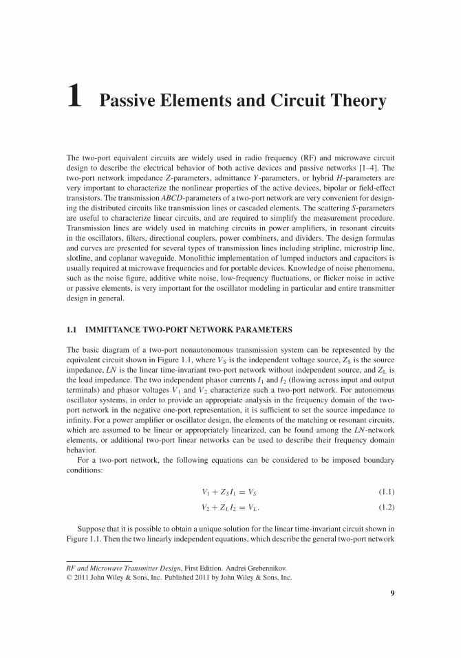
The basic diagram of a two-port nonautonomous transmission system can be represented by theequivalent circuit shown in Figure 1.1, where VS is the independent voltage source, ZS is the sourceimpedance, LN is the linear time-invariant two-port network without independent source, and ZL isthe load impedance. The two independent phasor currents I1 and I2 (flowing across input and outputterminals) and phasor voltages V1 and V2 characterize such a two-port network. For autonomousoscillator systems, in order to provide an appropriate analysis in the frequency domain of the two-port network in the negative one-port representation, it is sufficient to set the source impedance toinfinity. For a power amplifier or oscillator design, the elements of the matching or resonant circuits,which are assumed to be linear or appropriately linearized, can be found among the LN-networkelements, or additional two-port linear networks can be used to describe their frequency domainbehavior.
For a two-port network, the following equations can be considered to be imposed boundaryconditions:
V1 + ZS I1 = VS (1.1)
V2 + ZL I2 = VL . (1.2)
Suppose that it is possible to obtain a unique solution for the linear time-invariant circuit shown inFigure 1.1. Then the two linearly independent equations, which describe the general two-port network
RF and Microwave Transmitter Design, First Edition. Andrei Grebennikov.C© 2011 John Wiley & Sons, Inc. Published 2011 by John Wiley & Sons, Inc.
9
JWBS064-c01 JWBS064-Gerbennikov March 12, 2011 8:36 Printer Name: Yet to Come
10 PASSIVE ELEMENTS AND CIRCUIT THEORY
FIGURE 1.1 Basic diagram of two-port nonautonomous transmission system.
in terms of circuit variables V1, V2, I1, and I2, can be expressed in a matrix form as
[M] [V ] + [N ] [I ] = 0 (1.3)
or
m11V1 + m12V2 + n11 I1 + n12 I2 = 0
m21V1 + m22V2 + n21 I1 + n22 I2 = 0
}. (1.4)
The complex 2 × 2 matrices [M] and [N] in Eq. (1.3) are independent of the source and loadimpedances ZS and ZL and voltages VS and VL, respectively, and they depend only on the circuitelements inside the LN network.
If matrix [M] in Eq. (1.3) is nonsingular when |M| �= 0, then this matrix equation can be rewrittenin terms of [I] as
[V ] = − [M]−1 [N ] [I ] = [Z ] [I ] (1.5)
where [Z] is the open-circuit impedance two-port network matrix. In a scalar form, matrix Eq. (1.5)is given by
V1 = Z11 I1 + Z12 I2 (1.6)
V2 = Z21 I1 + Z22 I2 (1.7)
where Z11 and Z22 are the open-circuit driving-point impedances, and Z12 and Z21 are the open-circuittransfer impedances of the two-port network. The voltage components V1 and V2 due to the inputcurrent I1 can be found by setting I2 = 0 in Eqs. (1.6) and (1.7), resulting in an open-output terminal.Similarly, the same voltage components V1 and V2 are determined by setting I1 = 0 when the inputterminal becomes open-circuited. The resulting driving-point impedances can be written as
Z11 = V1
I1
∣∣∣∣I2=0
Z22 = V2
I2
∣∣∣∣I1=0
(1.8)
whereas the two transfer impedances are
Z21 = V2
I1
∣∣∣∣I2=0
Z12 = V1
I2
∣∣∣∣I1=0
. (1.9)
Dual analysis can be used to derive the short-circuit admittance matrix when the current compo-nents I1 and I2 are considered as outputs caused by V1 and V2. If matrix [N] in Eq. (1.3) is nonsingular
JWBS064-c01 JWBS064-Gerbennikov March 12, 2011 8:36 Printer Name: Yet to Come
IMMITTANCE TWO-PORT NETWORK PARAMETERS 11
when |N | �= 0, this matrix equation can be rewritten in terms of [V] as
[I ] = − [N ]−1 [M] [V ] = [Y ] [V ] (1.10)
where [Y] is the short-circuit admittance two-port network matrix. In a scalar form, matrix Eq. (1.10)is written as
I1 = Y11V1 + Y12V2 (1.11)
I2 = Y21V1 + Y22V2 (1.12)
where Y11 and Y22 are the short-circuit driving-point admittances, and Y12 and Y21 are the short-circuittransfer admittances of the two-port network. In this case, the current components I1 and I2 due to theinput voltage source V1 are determined by setting V2 = 0 in Eqs. (1.11) and (1.12), thus creating a shortoutput terminal. Similarly, the same current components I1 and I2 are determined by setting V1 = 0when input terminal becomes short-circuited. As a result, the two driving-point admittances are
Y11 = I1
V1
∣∣∣∣V2=0
Y22 = I2
V2
∣∣∣∣V1=0
(1.13)
whereas the two transfer admittances are
Y21 = I2
V1
∣∣∣∣V2=0
Y12 = I1
V2
∣∣∣∣V1=0
. (1.14)
In some cases, an equivalent two-port network representation can be redefined in order to expressthe voltage source V1 and output current I2 in terms of the input current I1 and output voltage V2. Ifthe submatrix
[m11 n12
m21 n22
]
given in Eq. (1.4) is nonsingular, then
[V1
I2
]= −
[m11 n12
m21 n22
]−1 [n11 m12
n21 m22
] [I1
V2
]= [H ]
[I1
V2
](1.15)
where [H] is the hybrid two-port network matrix. In a scalar form, it is best to represent matrix Eq.(1.15) as
V1 = h11 I1 + h12V2 (1.16)
I2 = h21 I1 + h22V2 (1.17)
where h11, h12, h21, and h22 are the hybrid H-parameters. The voltage source V1 and current componentI2 are determined by setting V2 = 0 for the short output terminal in Eqs. (1.16) and (1.17) as
h11 = V1
I1
∣∣∣∣V2=0
h21 = I2
I1
∣∣∣∣V2=0
(1.18)
where h11 is the driving-point input impedance and h21 is the forward current transfer function.Similarly, the input voltage source V1 and output current I2 are determined by setting I1 = 0 when
JWBS064-c01 JWBS064-Gerbennikov March 12, 2011 8:36 Printer Name: Yet to Come
12 PASSIVE ELEMENTS AND CIRCUIT THEORY
input terminal becomes open-circuited as
h12 = V1
V2
∣∣∣∣I1=0
h22 = I2
V2
∣∣∣∣I1=0
(1.19)
where h12 is the reverse voltage transfer function and h22 is the driving-point output admittance.The transmission parameters, often used for passive device analysis, are determined for the
independent input voltage source V1 and input current I1 in terms of the output voltage V2 and outputcurrent I2. In this case, if the submatrix
[m11 n11
m21 n21
]
given in Eq. (1.4) is nonsingular, we obtain
[V1
I1
]= −
[m11 n11
m21 n21
]−1 [m12 n12
m22 n22
] [V2
−I2
]= [ABCD]
[V2
−I2
](1.20)
where [ABCD] is the forward transmission two-port network matrix. In a scalar form, we can write
V1 = AV2 − B I2 (1.21)
I1 = CV2 − DI2 (1.22)
where A, B, C, and D are the transmission parameters. The voltage source V1 and current componentI1 are determined by setting I2 = 0 for the open output terminal in Eqs. (1.21) and (1.22) as
A = V1
V2
∣∣∣∣I2=0
C = I1
V2
∣∣∣∣I2=0
(1.23)
where A is the reverse voltage transfer function and C is the reverse transfer admittance. Similarly,the input independent variables V1 and I1 are determined by setting V2 = 0 when the output terminalis short-circuited as
B = V1
I2
∣∣∣∣V2=0
D = I1
I2
∣∣∣∣V2=0
(1.24)
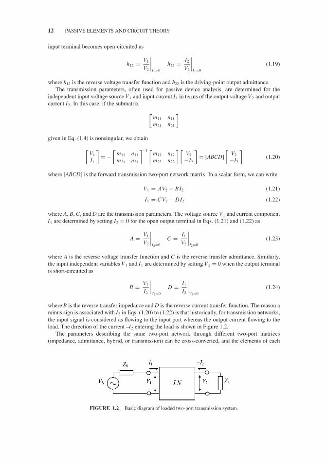
where B is the reverse transfer impedance and D is the reverse current transfer function. The reason aminus sign is associated with I2 in Eqs. (1.20) to (1.22) is that historically, for transmission networks,the input signal is considered as flowing to the input port whereas the output current flowing to theload. The direction of the current –I2 entering the load is shown in Figure 1.2.
The parameters describing the same two-port network through different two-port matrices(impedance, admittance, hybrid, or transmission) can be cross-converted, and the elements of each
FIGURE 1.2 Basic diagram of loaded two-port transmission system.