Embed Size (px)
Citation preview

“RF and Microwave System Design for A/D and Commercial Wireless applications”
Agilent EEsof EDA -European Microwave Week 2011 Workshop Series
Presenters: Stephen Slater, EEsof Application EngineerJake Sanderson, MPO Application Engineer
Group/Presentation Title
Month ##, 200XPage 2
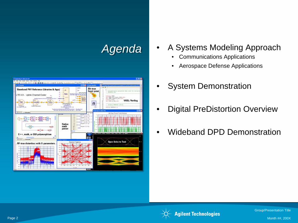
• A Systems Modeling Approach• Communications Applications• Aerospace Defense Applications
• System Demonstration
• Digital PreDistortion Overview
• Wideband DPD Demonstration
Agenda
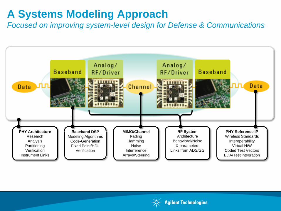
PHY ArchitectureResearch Analysis
PartitioningVerification
Instrument Links
MIMO/ChannelFading
JammingNoise
InterferenceArrays/Steering
A Systems Modeling ApproachFocused on improving system-level design for Defense & Communications
Baseband DSP Modeling Algorithms
Code-GenerationFixed Point/HDL
Verification
RF SystemArchitecture
Behavioral/NoiseX-parameters
Links from ADS/GG
PHY Reference IPWireless Standards
InteroperabilityVirtual H/W
Coded Test VectorsEDA/Test integration
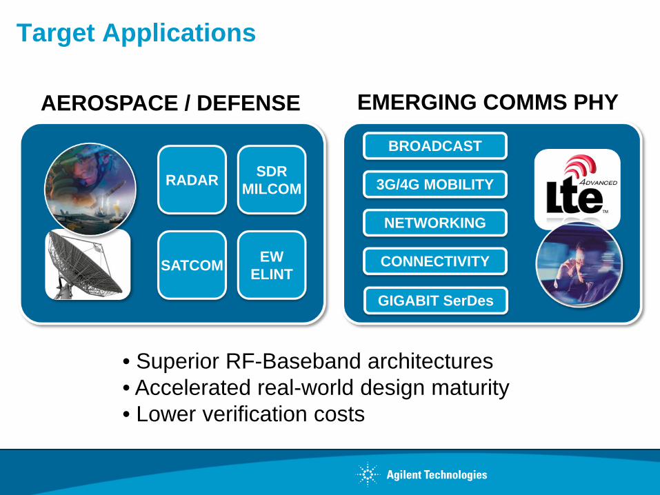
Target Applications
AEROSPACE / DEFENSE EMERGING COMMS PHY
SDRMILCOM
SATCOM EWELINT
BROADCAST
3G/4G MOBILITY
NETWORKING
CONNECTIVITY
RADAR
• Superior RF-Baseband architectures• Accelerated real-world design maturity• Lower verification costs
GIGABIT SerDes
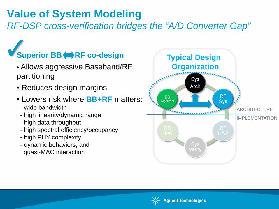
Superior BB RF co-design• Allows aggressive Baseband/RF partitioning • Reduces design margins • Lowers risk where BB+RF matters:
- wide bandwidth- high linearity/dynamic range- high data throughput - high spectral efficiency/occupancy- high PHY complexity- dynamic behaviors, and
quasi-MAC interaction
Value of System Modeling RF-DSP cross-verification bridges the “A/D Converter Gap”
Typical DesignOrganization
ARCHITECTURE
IMPLEMENTATION
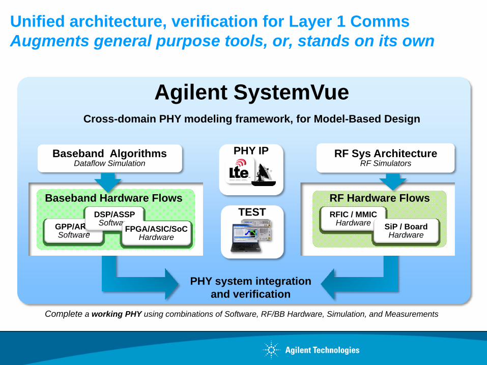
Unified architecture, verification for Layer 1 CommsAugments general purpose tools, or, stands on its own
PHY system integrationand verification
Cross-domain PHY modeling framework, for Model-Based Design
Complete a working PHY using combinations of Software, RF/BB Hardware, Simulation, and Measurements
Baseband AlgorithmsDataflow Simulation
RF Sys ArchitectureRF Simulators
Agilent SystemVue
PHY IP
TESTRF Hardware FlowsRFIC / MMIC
Hardware SiP / BoardHardware
Baseband Hardware Flows
GPP/ARMSoftware
DSP/ASSPSoftware
FPGA/ASIC/SoCHardware
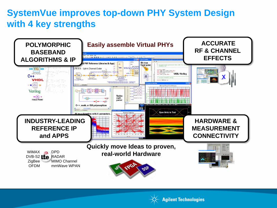
SystemVue improves top-down PHY System Design with 4 key strengths
Easily assemble Virtual PHYs
Quickly move Ideas to proven, real-world HardwareWiMAX
DVB-S2ZigBeeOFDM
DPDRADARMIMO ChannelmmWave WPAN
HARDWARE & MEASUREMENTCONNECTIVITY
INDUSTRY-LEADING REFERENCE IP
and APPS
POLYMORPHICBASEBAND
ALGORITHMS & IP
ACCURATE RF & CHANNEL
EFFECTS
.bitFiles
FPGASynthesis
Handwritten HDL
Custom IP
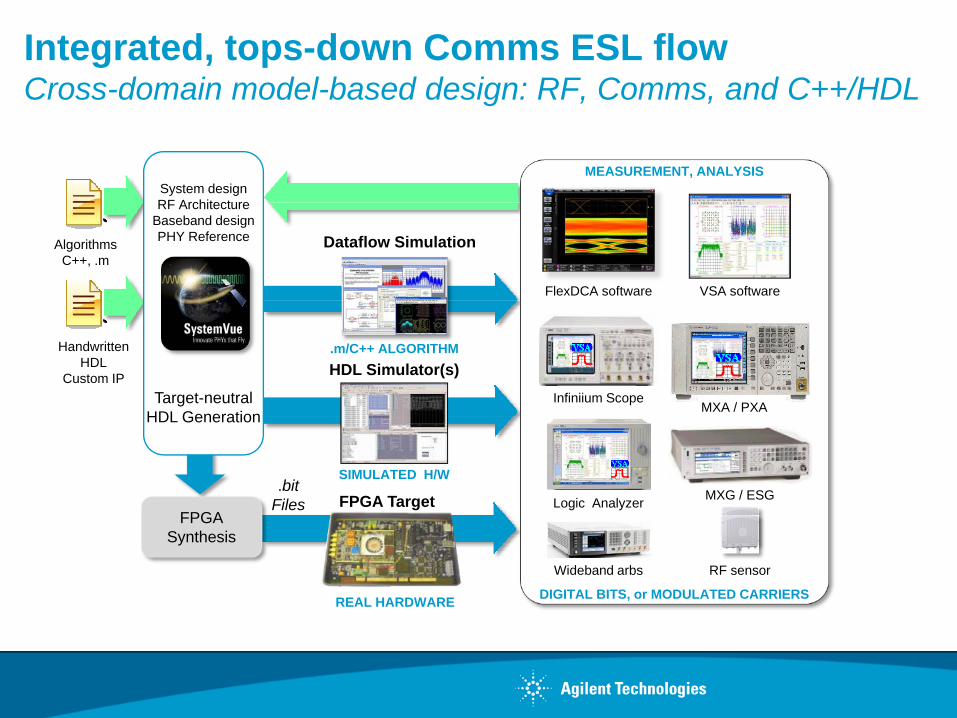
Integrated, tops-down Comms ESL flow Cross-domain model-based design: RF, Comms, and C++/HDL
FPGA Target
REAL HARDWARE
HDL Simulator(s)
SIMULATED H/W
Dataflow Simulation
.m/C++ ALGORITHM
AlgorithmsC++, .m
Target-neutralHDL Generation
System designRF Architecture
Baseband designPHY Reference
MEASUREMENT, ANALYSIS
VSA softwareFlexDCA software
DIGITAL BITS, or MODULATED CARRIERS
MXG / ESG
Infiniium Scope
Logic Analyzer
MXA / PXA
Wideband arbs RF sensor
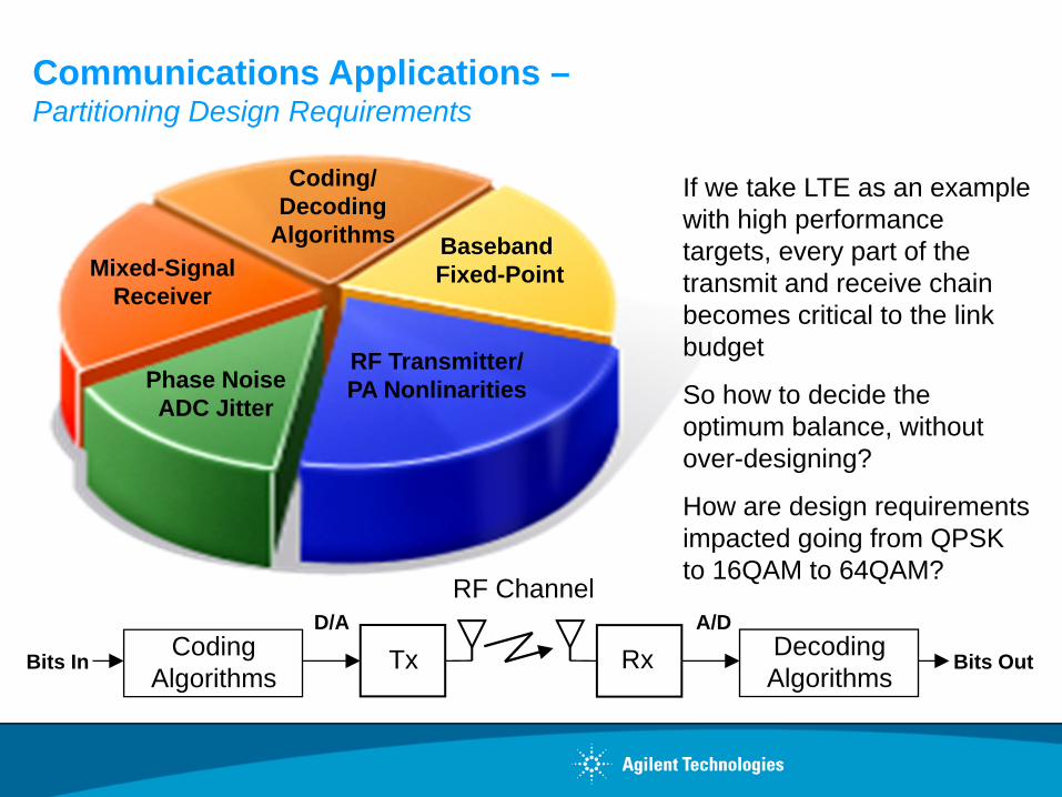
Communications Applications –Partitioning Design Requirements
Phase NoiseADC Jitter
RF Transmitter/PA Nonlinarities
Baseband Fixed-PointMixed-Signal
Receiver
Tx RxCodingAlgorithms
D/A
Bits In DecodingAlgorithms
Bits Out
RF ChannelA/D
Coding/Decoding
Algorithms
If we take LTE as an example with high performance targets, every part of the transmit and receive chain becomes critical to the link budget
So how to decide the optimum balance, without over-designing?
How are design requirements impacted going from QPSK to 16QAM to 64QAM?
Coding/Decoding
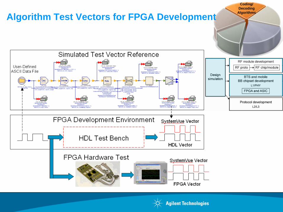
AlgorithmsAlgorithm Test Vectors for FPGA Development
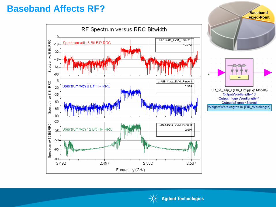
Baseband Affects RF? Baseband Fixed-Point
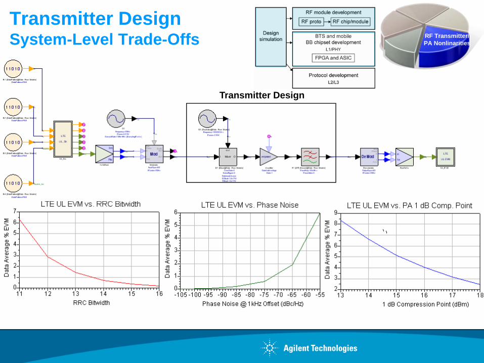
Transmitter Design System-Level Trade-Offs
Transmitter Design
RF Transmitter/PA Nonlinarities
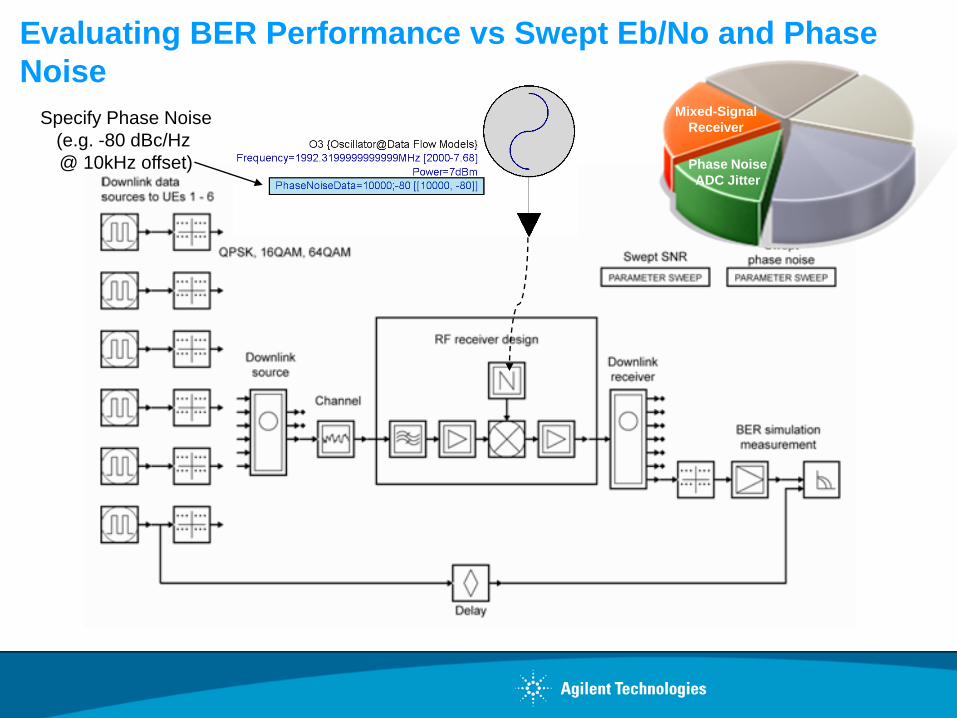
Evaluating BER Performance vs Swept Eb/No and Phase Noise
Specify Phase Noise(e.g. -80 dBc/Hz @ 10kHz offset) Phase Noise
ADC Jitter
Mixed-SignalReceiver
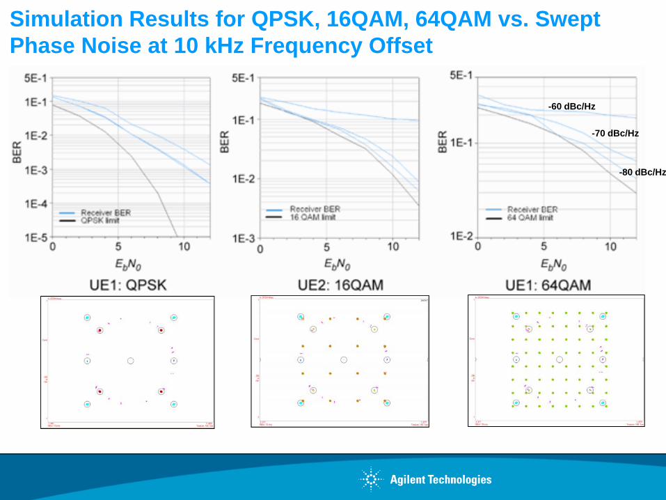
Simulation Results for QPSK, 16QAM, 64QAM vs. Swept Phase Noise at 10 kHz Frequency Offset
-60 dBc/Hz
-70 dBc/Hz
-80 dBc/Hz
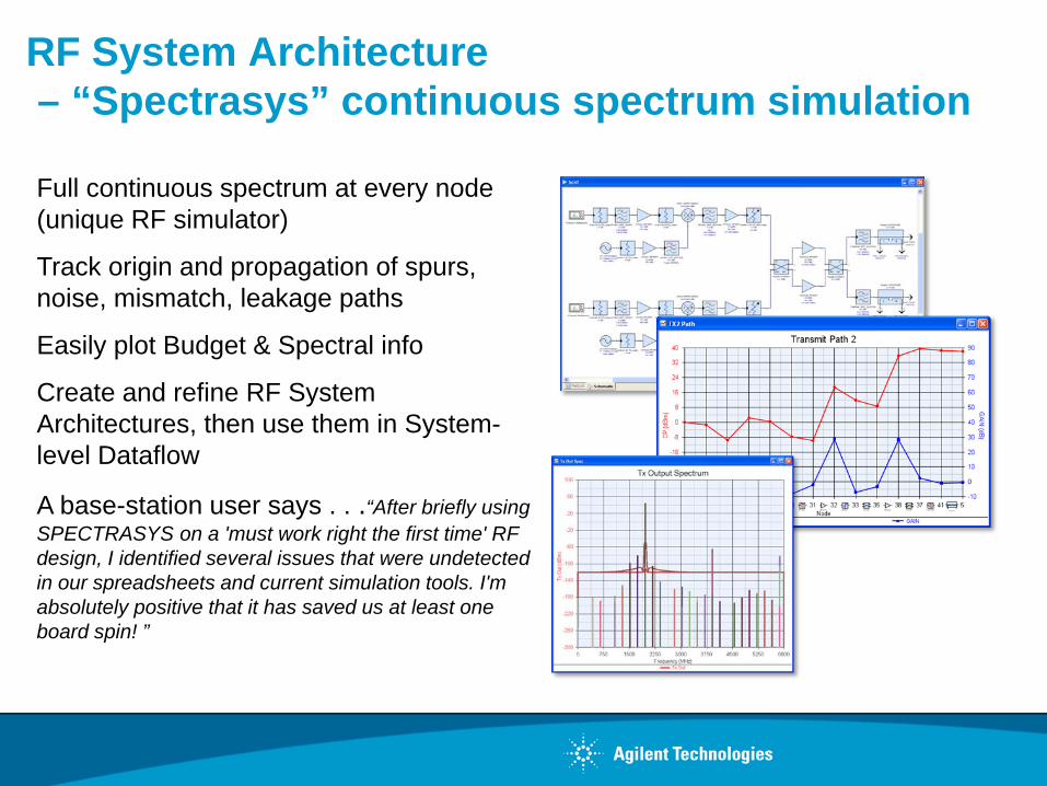
RF System Architecture– “Spectrasys” continuous spectrum simulation
Full continuous spectrum at every node (unique RF simulator)
Track origin and propagation of spurs, noise, mismatch, leakage paths
Easily plot Budget & Spectral info
Create and refine RF System Architectures, then use them in System-level Dataflow
A base-station user says . . .“After briefly using SPECTRASYS on a 'must work right the first time' RF design, I identified several issues that were undetected in our spreadsheets and current simulation tools. I'm absolutely positive that it has saved us at least one board spin! ”
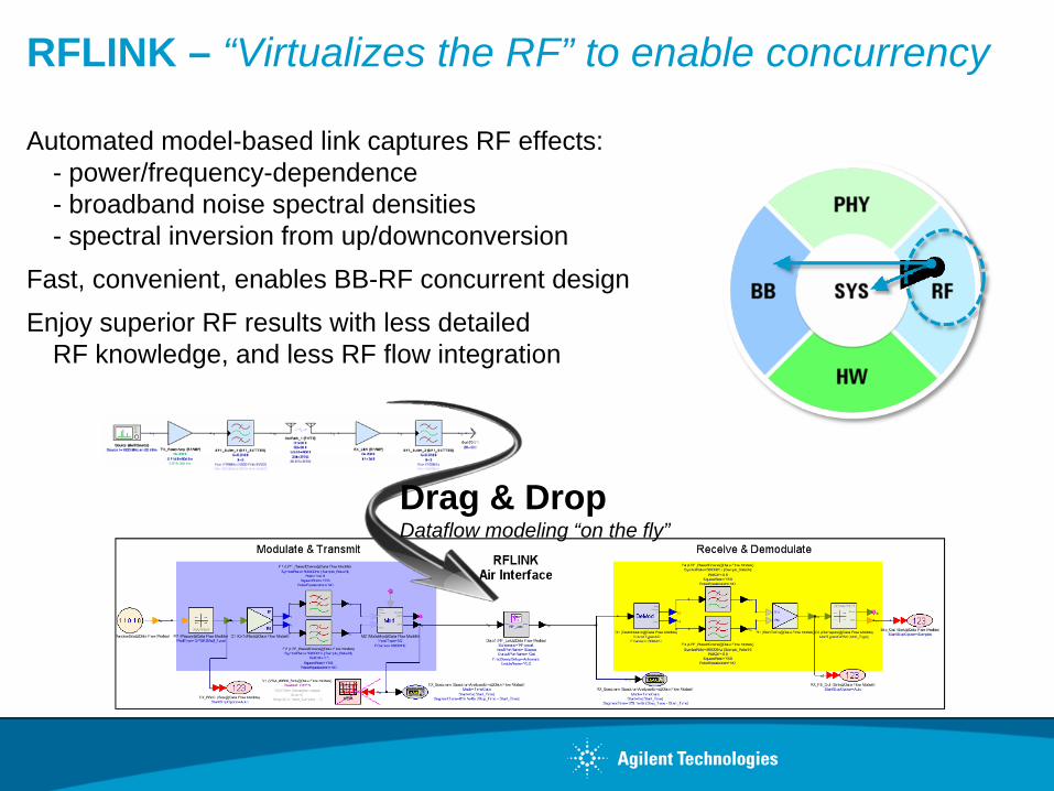
RFLINK – “Virtualizes the RF” to enable concurrency
Drag & DropDataflow modeling “on the fly”
Automated model-based link captures RF effects: - power/frequency-dependence- broadband noise spectral densities- spectral inversion from up/downconversion
Fast, convenient, enables BB-RF concurrent designEnjoy superior RF results with less detailed
RF knowledge, and less RF flow integration
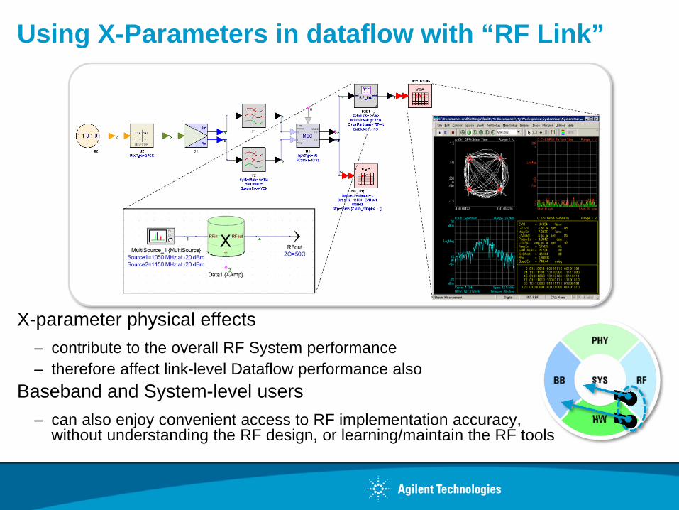
Using X-Parameters in dataflow with “RF Link”
X-parameter physical effects – contribute to the overall RF System performance– therefore affect link-level Dataflow performance also
Baseband and System-level users – can also enjoy convenient access to RF implementation accuracy,
without understanding the RF design, or learning/maintain the RF tools
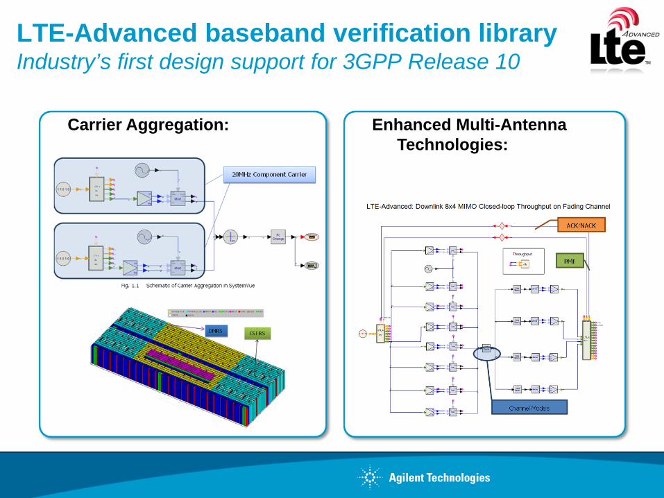
LTE-Advanced baseband verification libraryIndustry’s first design support for 3GPP Release 10
Carrier Aggregation: Enhanced Multi-Antenna Technologies:
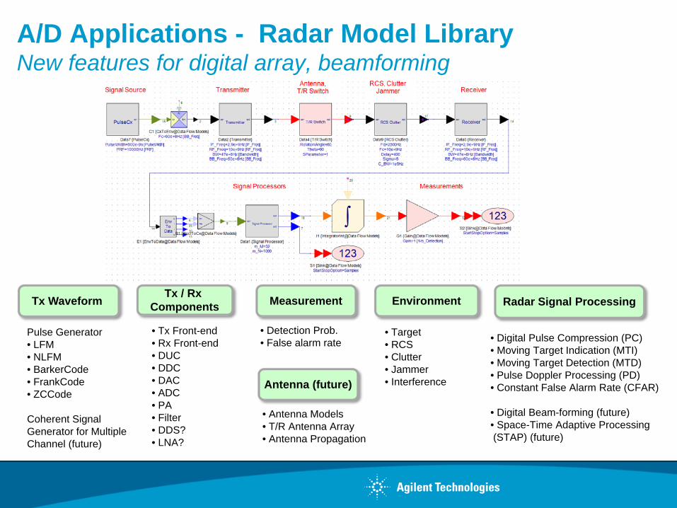
A/D Applications - Radar Model LibraryNew features for digital array, beamforming
Tx Waveform Tx / Rx Components Measurement
Pulse Generator • LFM• NLFM• BarkerCode• FrankCode• ZCCode
Coherent Signal Generator for Multiple Channel (future)
• Tx Front-end• Rx Front-end• DUC• DDC• DAC• ADC• PA• Filter• DDS?• LNA?
Environment Radar Signal Processing
• Detection Prob.• False alarm rate
• Target• RCS• Clutter• Jammer• Interference
• Digital Pulse Compression (PC)• Moving Target Indication (MTI)• Moving Target Detection (MTD)• Pulse Doppler Processing (PD)• Constant False Alarm Rate (CFAR)
• Digital Beam-forming (future)• Space-Time Adaptive Processing (STAP) (future)
Antenna (future)
• Antenna Models• T/R Antenna Array• Antenna Propagation
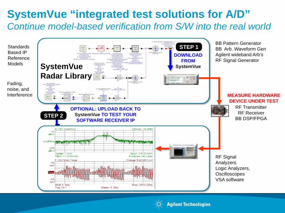
SystemVue “integrated test solutions for A/D”Continue model-based verification from S/W into the real world
RF Signal AnalyzersLogic Analyzers, OscilloscopesVSA software
OPTIONAL: UPLOAD BACK TOSystemVue TO TEST YOUR SOFTWARE RECEIVER IP
StandardsBased IPReference Models
Fading, noise, and Interference
BB Pattern Generator BB Arb. Waveform GenAgilent wideband Arb’sRF Signal Generator
DOWNLOADFROM
SystemVueSystemVueRadar Library
RF TransmitterRF Receiver
BB DSP/FPGA
MEASURE HARDWARE DEVICE UNDER TEST
STEP 1
STEP 2
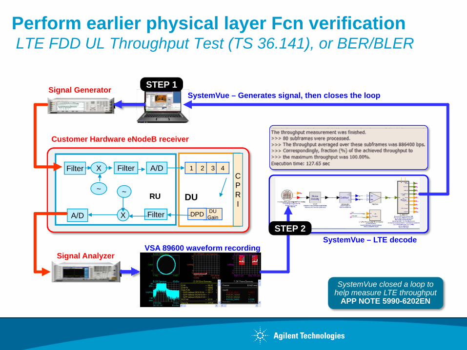
Perform earlier physical layer Fcn verification LTE FDD UL Throughput Test (TS 36.141), or BER/BLER
Filter X
~
Filter A/D 1 2 3 4
DUGainDPDFilterX
~
A/D
RU DU
CPRI
Signal Generator
Signal Analyzer
SystemVue – Generates signal, then closes the loop
VSA 89600 waveform recordingSystemVue – LTE decode
Customer Hardware eNodeB receiver
STEP 1
STEP 2
SystemVue closed a loop to help measure LTE throughput
APP NOTE 5990-6202EN
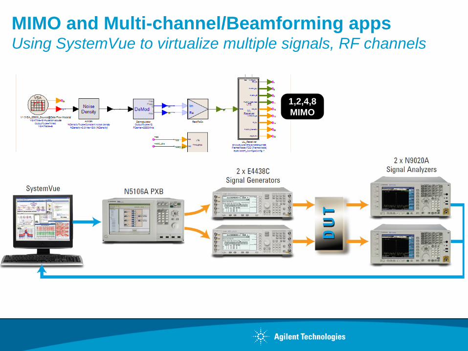
MIMO and Multi-channel/Beamforming appsUsing SystemVue to virtualize multiple signals, RF channels
1,2,4,8MIMO
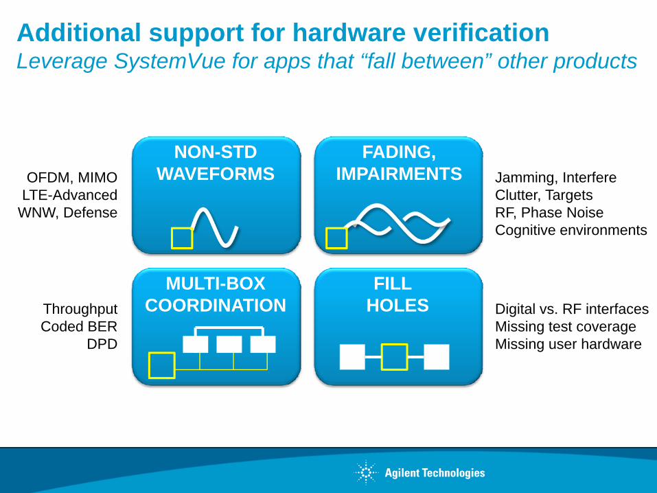
Additional support for hardware verificationLeverage SystemVue for apps that “fall between” other products
FILL HOLES
OFDM, MIMOLTE-Advanced
WNW, Defense
Jamming, InterfereClutter, TargetsRF, Phase NoiseCognitive environments
ThroughputCoded BER
DPD
MULTI-BOXCOORDINATION Digital vs. RF interfaces
Missing test coverageMissing user hardware
NON-STDWAVEFORMS
FADING,IMPAIRMENTS
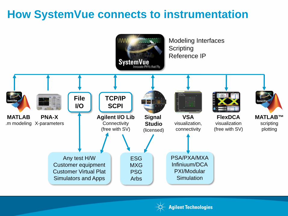
How SystemVue connects to instrumentation
MATLAB.m modeling
Signal Studio
(licensed)
VSAvisualization,connectivity
TCP/IPSCPI
FlexDCAvisualization
(free with SV)
MATLAB™scriptingplotting
Agilent I/O LibConnectivity
(free with SV)
PSA/PXA/MXAInfiniuum/DCAPXI/ModularSimulation
Any test H/WCustomer equipmentCustomer Virtual PlatSimulators and Apps
File I/O
ESGMXGPSGArbs
Modeling InterfacesScriptingReference IP
PNA-XX-parameters
Group/Presentation Title
Month ##, 200XPage 25
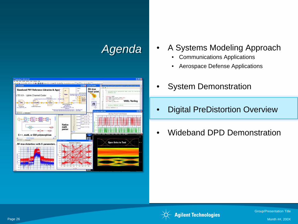
• A Systems Modeling Approach• Communications Applications• Aerospace Defense Applications
• System Demonstration
• Digital PreDistortion Overview
• Wideband DPD Demonstration
Agenda
Group/Presentation Title
Month ##, 200XPage 26
• A Systems Modeling Approach• Communications Applications• Aerospace Defense Applications
• System Demonstration
• Digital PreDistortion Overview
• Wideband DPD Demonstration
Agenda
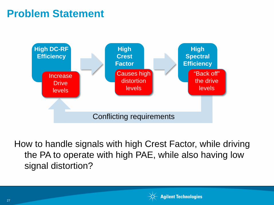
Conflicting requirements
Problem Statement
27
How to handle signals with high Crest Factor, while driving the PA to operate with high PAE, while also having low signal distortion?
High DC-RF Efficiency
HighCrest Factor
HighSpectral
Efficiency
IncreaseDrive levels
Causes high distortion
levels
“Back off” the drive
levels
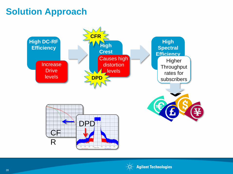
Solution Approach
28
High DC-RF Efficiency High
Crest Factor
HighSpectral
Efficiency
IncreaseDrive levels
Causes high distortion
levels
Higher Throughput
rates for subscribers
CFR
DPD
CFR
DPD
29
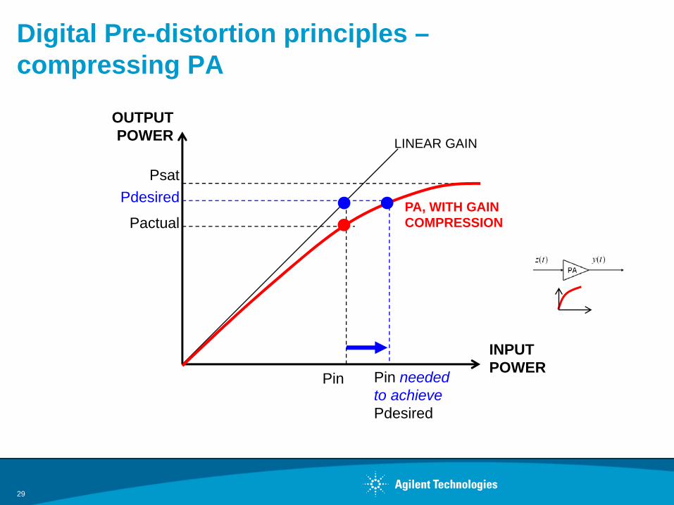
Psat
Pin
LINEAR GAIN
INPUT POWER
OUTPUTPOWER
Pdesired
Pactual
Pin neededto achieve Pdesired
PA, WITH GAINCOMPRESSION
Digital Pre-distortion principles –compressing PA
30
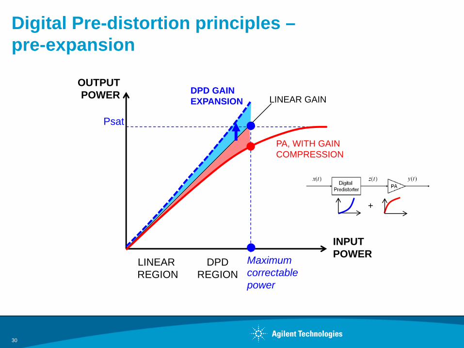
Digital Pre-distortion principles –pre-expansion
Maximum correctablepower
Psat
LINEAR GAIN
INPUT POWER
OUTPUTPOWER
LINEAR REGION
DPDREGION
PA, WITH GAINCOMPRESSION
DPD GAINEXPANSION
+
31
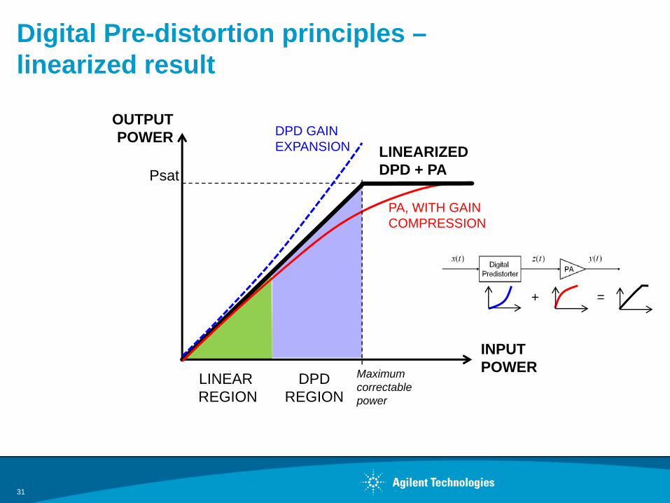
Maximum correctablepower
Psat
INPUT POWER
OUTPUTPOWER
LINEAR REGION
DPDREGION
LINEARIZEDDPD + PA
Digital Pre-distortion principles –linearized result
PA, WITH GAINCOMPRESSION
DPD GAINEXPANSION
+ =
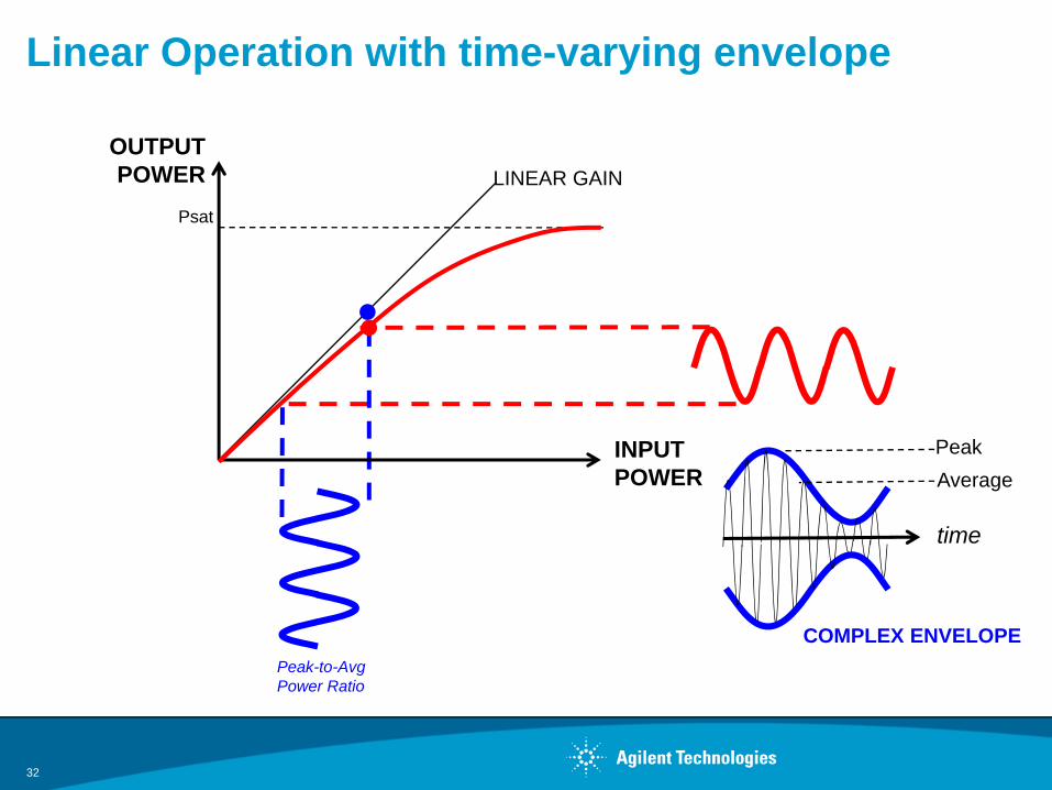
Linear Operation with time-varying envelope
32
Psat
LINEAR GAIN
INPUT POWER
OUTPUTPOWER
Peak-to-AvgPower Ratio
COMPLEX ENVELOPE
time
PeakAverage
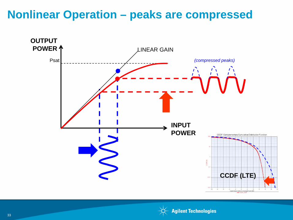
Nonlinear Operation – peaks are compressed
33
Psat
LINEAR GAIN
INPUT POWER
OUTPUTPOWER
(compressed peaks)
CCDF (LTE)
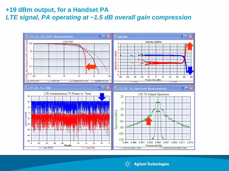
+19 dBm output, for a Handset PALTE signal, PA operating at ~1.5 dB overall gain compression
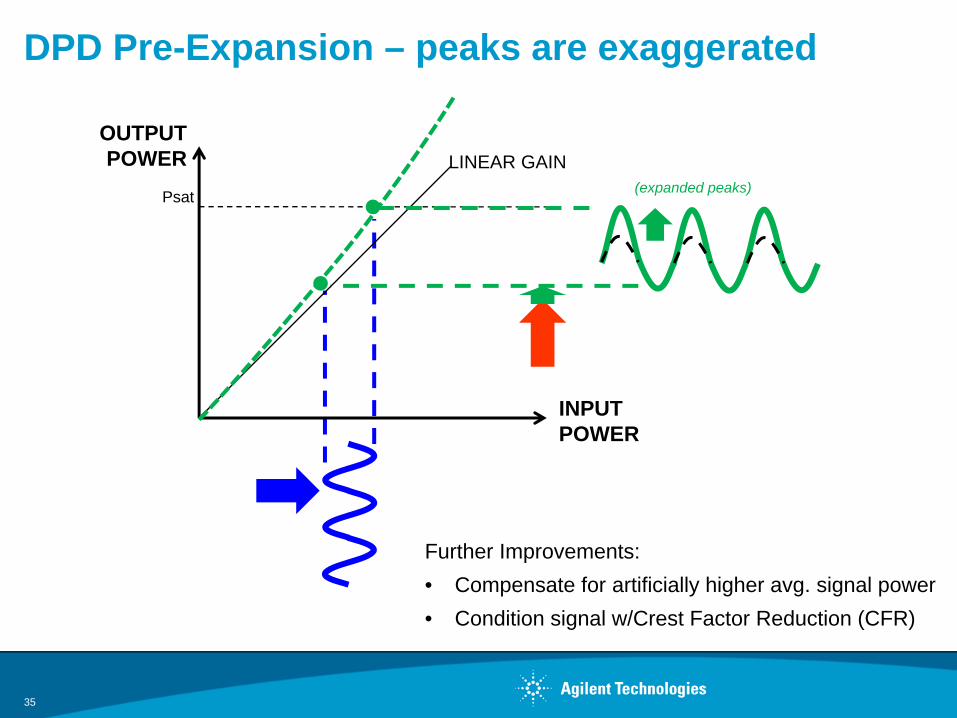
DPD Pre-Expansion – peaks are exaggerated
35
Psat
LINEAR GAIN
INPUT POWER
OUTPUTPOWER
Further Improvements:• Compensate for artificially higher avg. signal power • Condition signal w/Crest Factor Reduction (CFR)
(expanded peaks)
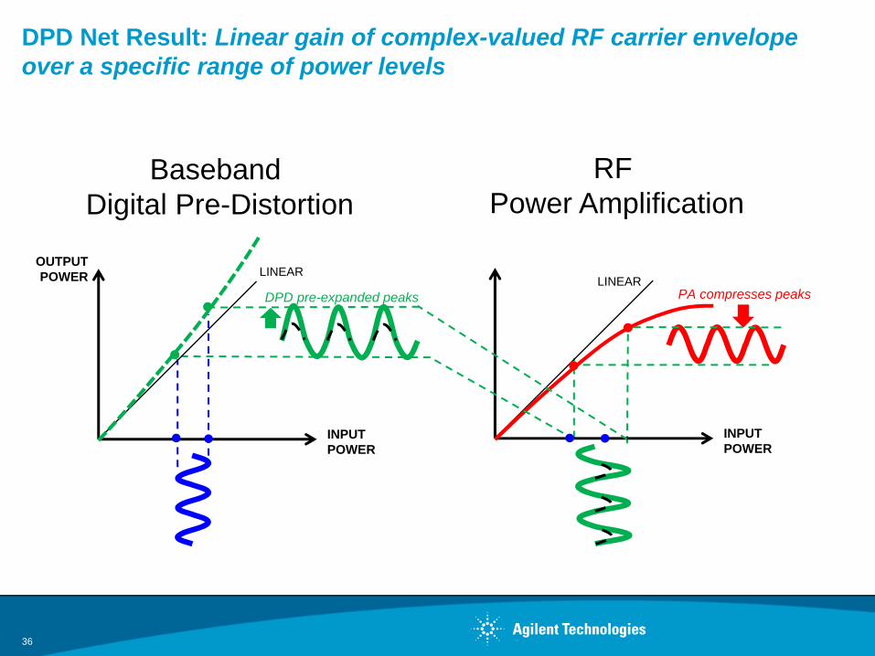
DPD Net Result: Linear gain of complex-valued RF carrier envelope over a specific range of power levels
36
LINEAR
INPUT POWER
OUTPUTPOWER
DPD pre-expanded peaks
INPUT POWER
PA compresses peaksLINEAR
Baseband Digital Pre-Distortion
RF Power Amplification
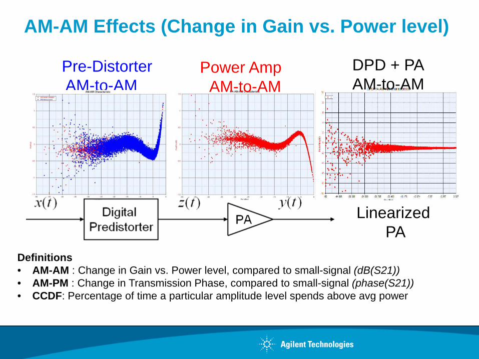
AM-AM Effects (Change in Gain vs. Power level)
Pre-Distorter AM-to-AM
DPD + PAAM-to-AM
Linearized PA
Power Amp AM-to-AM
Definitions• AM-AM : Change in Gain vs. Power level, compared to small-signal (dB(S21))• AM-PM : Change in Transmission Phase, compared to small-signal (phase(S21))• CCDF: Percentage of time a particular amplitude level spends above avg power
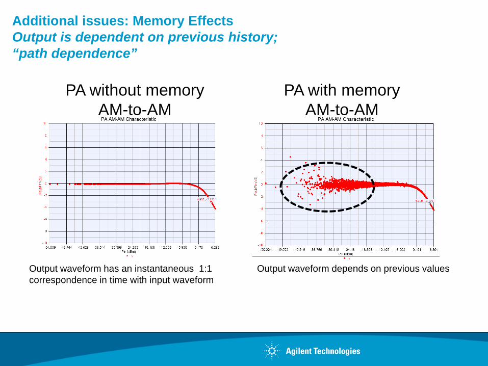
Additional issues: Memory EffectsOutput is dependent on previous history; “path dependence”
PA with memoryAM-to-AM
PA without memoryAM-to-AM
Output waveform has an instantaneous 1:1 correspondence in time with input waveform
Output waveform depends on previous values
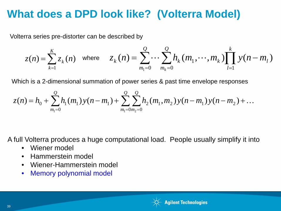
What does a DPD look like? (Volterra Model)
39
∑=
=K
kk nznz
1)()( ∑ ∑ ∏
= = =
−=Q
m
Q
m
k
llkkk
k
mnymmhnz0 0 1
11
)(),,()( LL
∑∑∑= ==
+−−+−+=Q
m
Q
m
Q
mmnymnymmhmnymhhnz
0 021212
01110
1 21
)()(),()()()( K
Volterra series pre-distorter can be described by
where
Which is a 2-dimensional summation of power series & past time envelope responses
A full Volterra produces a huge computational load. People usually simplify it into• Wiener model • Hammerstein model • Wiener-Hammerstein model• Memory polynomial model

DPD principles – Memory Polynomial Model
If only diagonal terms are kept, Volterra reduces to “Memory polynomial” model.
Agilent uses an indirect learning algorithm to extract MP coefficients.
As of SystemVue 2011.10, you can now add your own model, extraction algorithm, and even create your own GUI.
40
L. Ding, G. T. Zhou, D. R. Morgan, Z. Ma, J. S. Kenney, J. Kim, and C. R. Giardina, “Memory polynomial predistorter based on the indirect learning architecture,” in Proc. of GLOBECOM, Taipei, Taiwan, 2002, vol. 1, pp. 967–971.
∑∑= =
−−−=K
k
Q
q
kkq qnyqnyanz
1 0
1)()()(
Where• K is Nonlinearity order • Q is Memory length
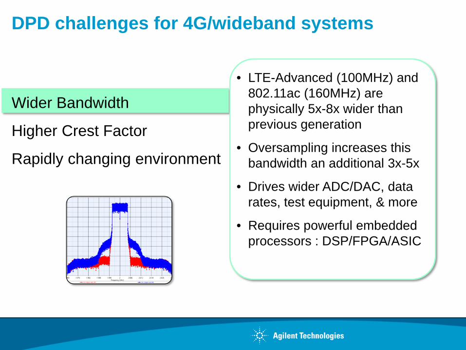
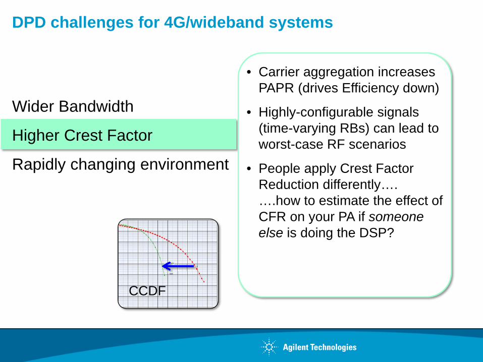
DPD challenges for 4G/wideband systems
• LTE-Advanced (100MHz) and 802.11ac (160MHz) are physically 5x-8x wider than previous generation
• Oversampling increases this bandwidth an additional 3x-5x
• Drives wider ADC/DAC, data rates, test equipment, & more
• Requires powerful embedded processors : DSP/FPGA/ASIC
Wider Bandwidth
Higher Crest Factor
Rapidly changing environment
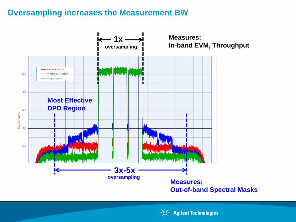
Oversampling increases the Measurement BW
1x
3x-5x
oversampling
oversampling
Measures: In-band EVM, Throughput
Measures:Out-of-band Spectral Masks
Most Effective DPD Region
DPD challenges for 4G/wideband systems
• Carrier aggregation increases PAPR (drives Efficiency down)
• Highly-configurable signals (time-varying RBs) can lead to worst-case RF scenarios
• People apply Crest Factor Reduction differently….….how to estimate the effect of CFR on your PA if someone else is doing the DSP?
Wider Bandwidth
Higher Crest Factor
Rapidly changing environment
CCDF
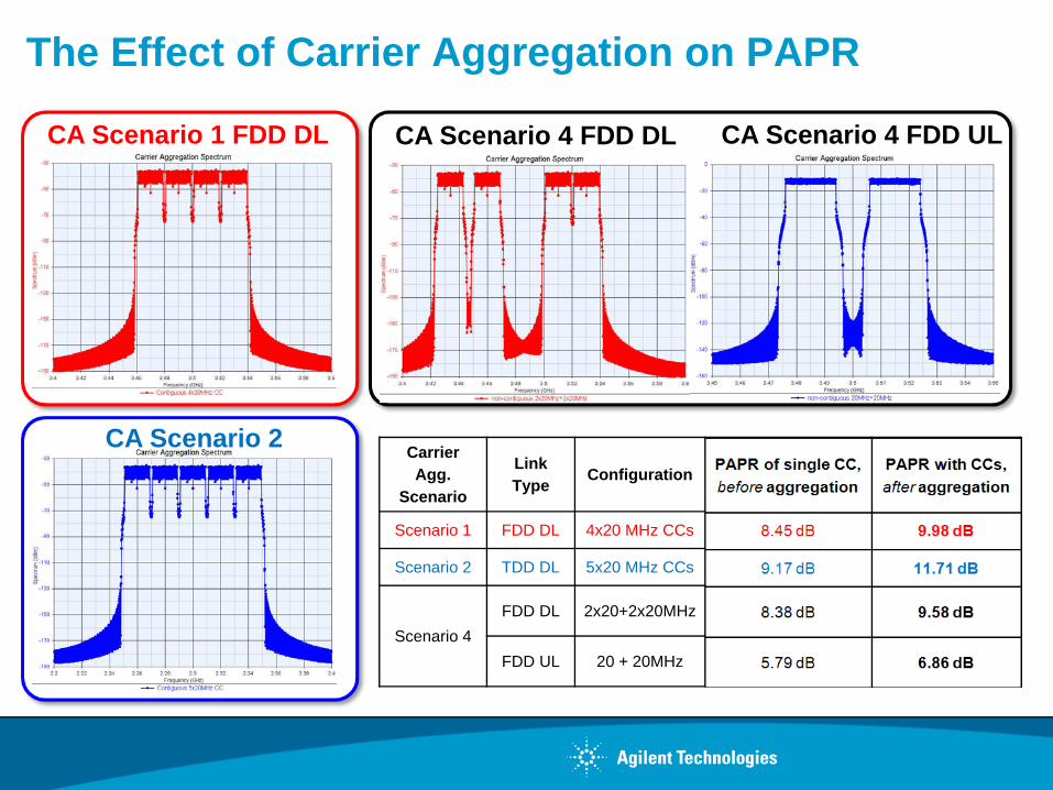
The Effect of Carrier Aggregation on PAPR
CarrierAgg.
Scenario
LinkType Configuration
PAPR of single CC,before aggregation
PAPR with CCs, after aggregation
Scenario 1 FDD DL 4x20 MHz CCs 8.45 dB 9.98 dB
Scenario 2 TDD DL 5x20 MHz CCs 9.17 dB 11.71 dB
Scenario 4 FDD DL 2x20+2x20MHz 8.38 dB 9.58 dB
FDD UL 20 + 20MHz 5.79 dB 6.86 dB
CA Scenario 1 FDD DL
CA Scenario 2 TDD DL
CA Scenario 4 FDD DL CA Scenario 4 FDD UL
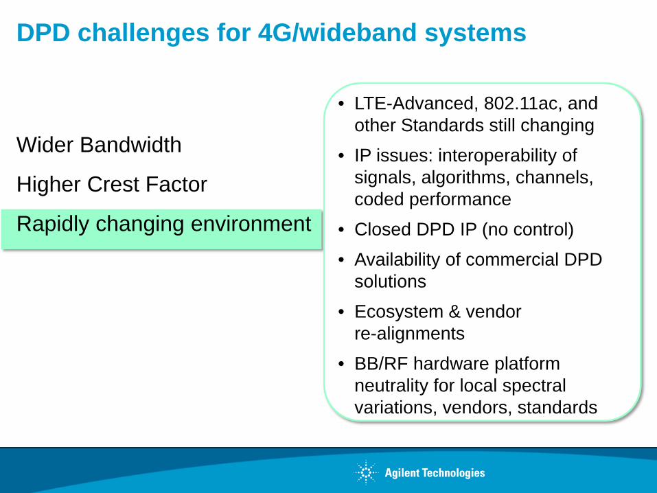
DPD challenges for 4G/wideband systems
• LTE-Advanced, 802.11ac, and other Standards still changing
• IP issues: interoperability of signals, algorithms, channels, coded performance
• Closed DPD IP (no control)• Availability of commercial DPD
solutions • Ecosystem & vendor
re-alignments • BB/RF hardware platform
neutrality for local spectral variations, vendors, standards
Wider Bandwidth
Higher Crest Factor
Rapidly changing environment
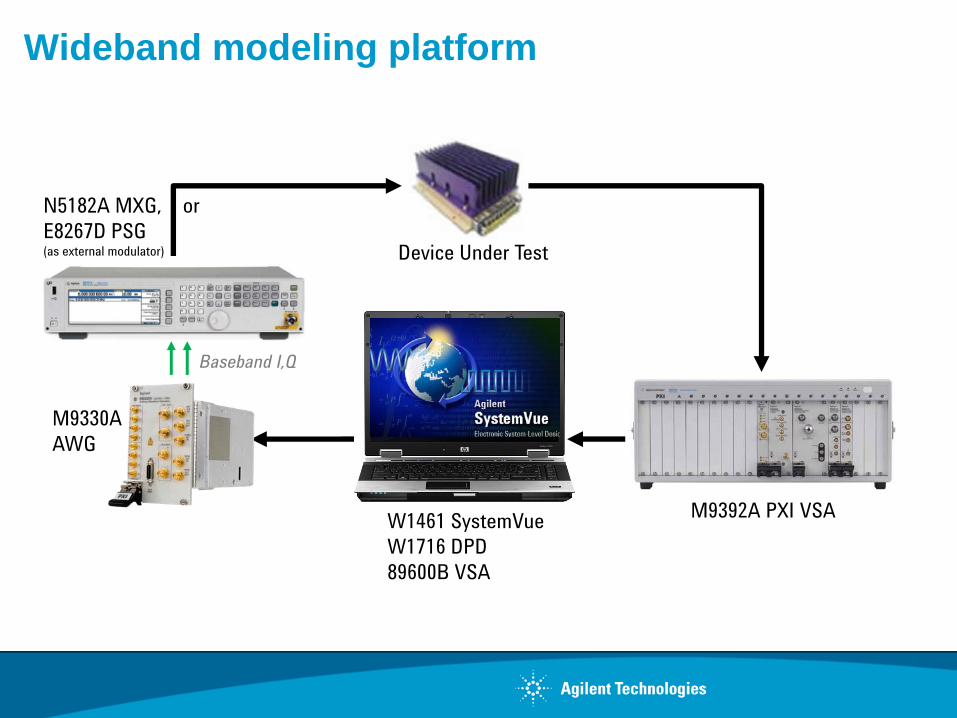
Wideband modeling platform
N5182A MXG, orE8267D PSG(as external modulator)
W1461 SystemVueW1716 DPD89600B VSA
M9330A AWG
M9392A PXI VSA
Device Under Test
Baseband I,Q
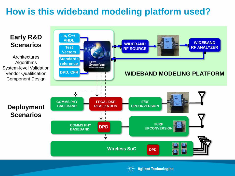
How is this wideband modeling platform used?
WIDEBAND MODELING PLATFORM
WIDEBANDRF SOURCE
WIDEBANDRF ANALYZER
.m, C++, VHDL
Test Vectors
Standards reference
DPD, CFR
Early R&DScenarios
ArchitecturesAlgorithms
System-level ValidationVendor QualificationComponent Design
DeploymentScenarios
COMMS PHY …..BASEBAND
IF/RFUPCONVERSIONDPD
COMMS PHYBASEBAND
IF/RFUPCONVERSION
FPGA / DSPREALIZATION
Wireless SoC DPD
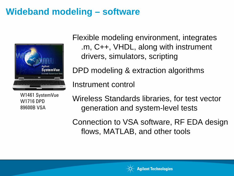
Wideband modeling – software
Flexible modeling environment, integrates .m, C++, VHDL, along with instrument drivers, simulators, scripting
DPD modeling & extraction algorithms
Instrument control
Wireless Standards libraries, for test vector generation and system-level tests
Connection to VSA software, RF EDA design flows, MATLAB, and other tools
W1461 SystemVueW1716 DPD89600B VSA
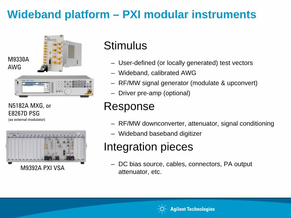
Wideband platform – PXI modular instruments
Stimulus– User-defined (or locally generated) test vectors– Wideband, calibrated AWG– RF/MW signal generator (modulate & upconvert)– Driver pre-amp (optional)
Response– RF/MW downconverter, attenuator, signal conditioning– Wideband baseband digitizer
Integration pieces– DC bias source, cables, connectors, PA output
attenuator, etc.
M9330A AWG
M9392A PXI VSA
N5182A MXG, orE8267D PSG(as external modulator)
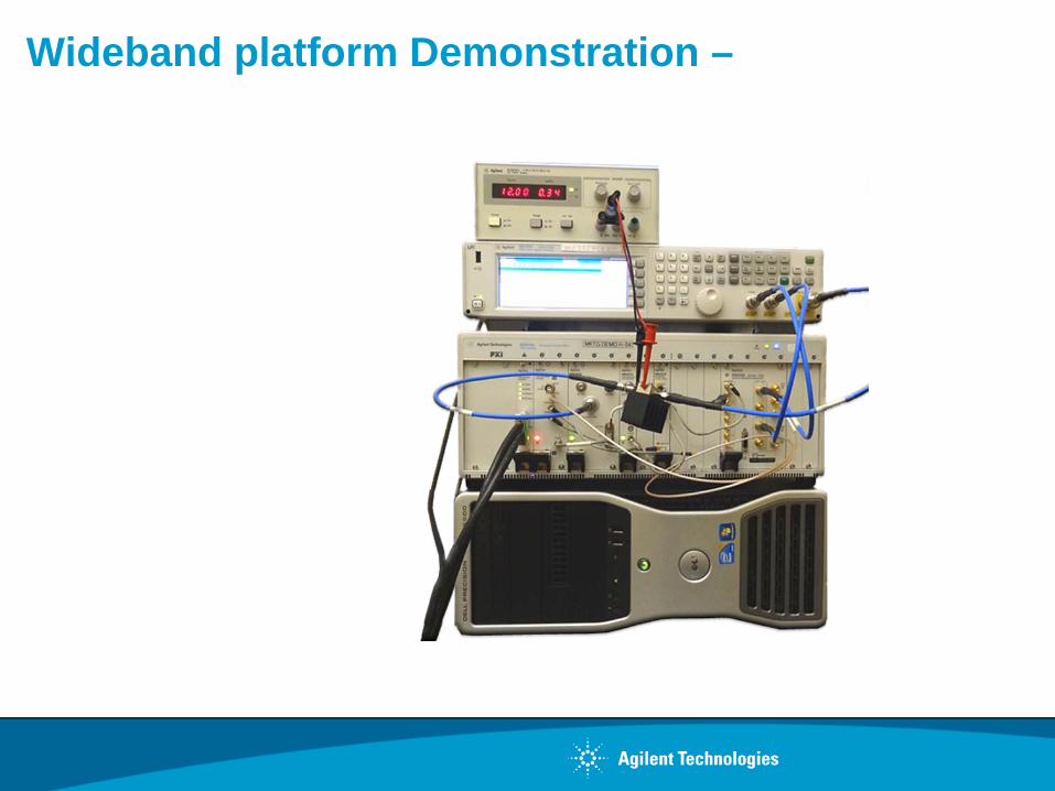
Wideband platform Demonstration –
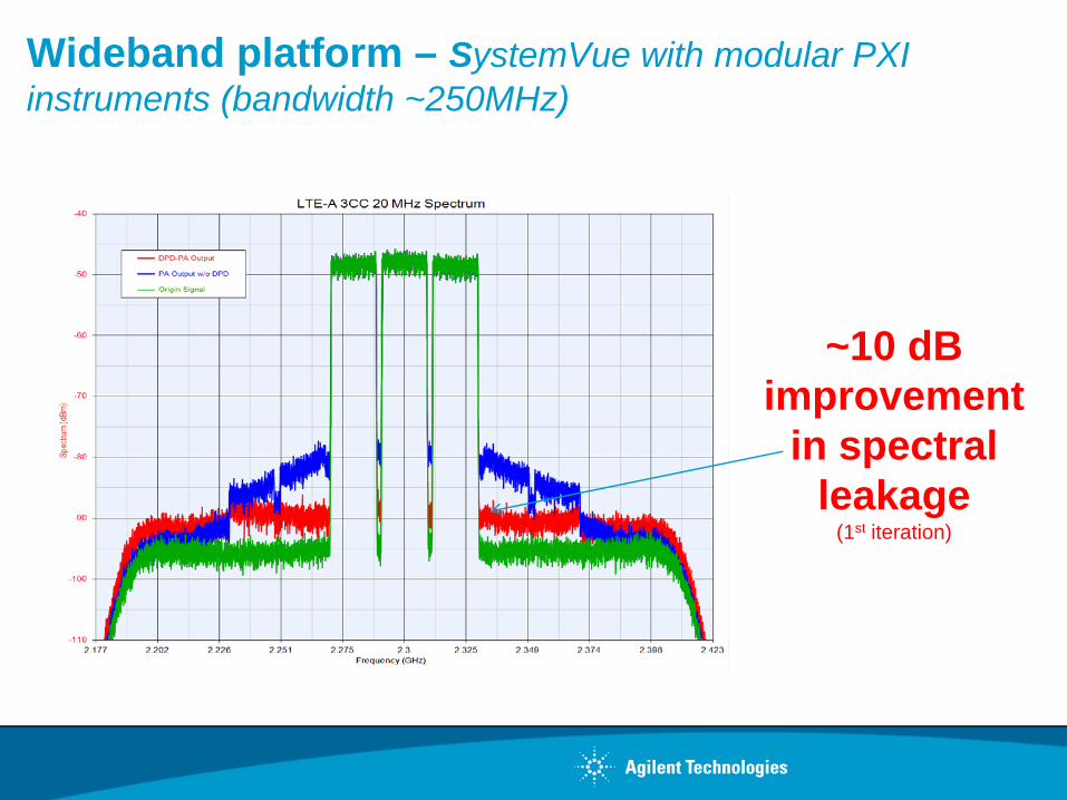
Wideband platform – SystemVue with modular PXI instruments (bandwidth ~250MHz)
~10 dB improvement
in spectral leakage
(1st iteration)
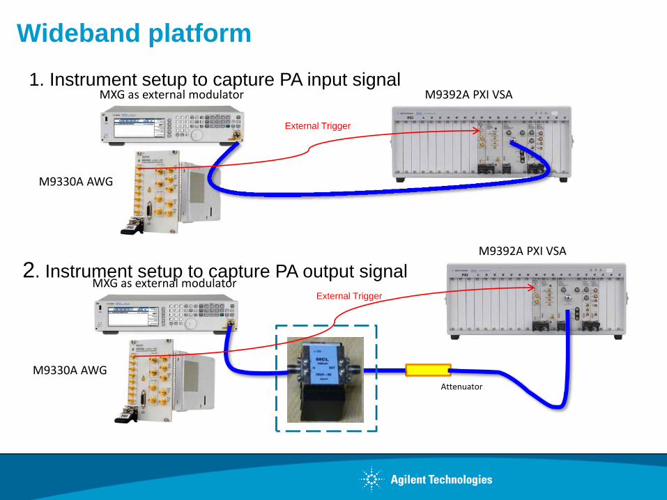
1. Instrument setup to capture PA input signal
2. Instrument setup to capture PA output signal
Wideband platform
External Trigger
M9330A AWG
MXG as external modulator M9392A PXI VSA
M9392A PXI VSA
External Trigger
Attenuator
M9330A AWG
MXG as external modulator
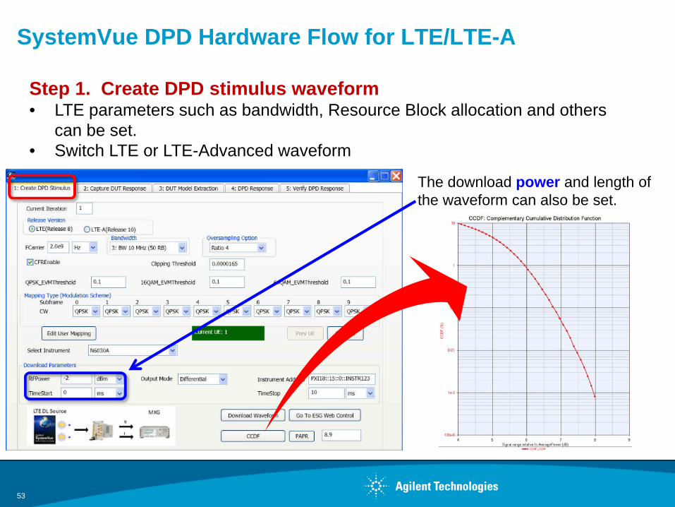
SystemVue DPD Hardware Flow for LTE/LTE-A
The download power and length of the waveform can also be set.
53
Step 1. Create DPD stimulus waveform• LTE parameters such as bandwidth, Resource Block allocation and others
can be set.• Switch LTE or LTE-Advanced waveform
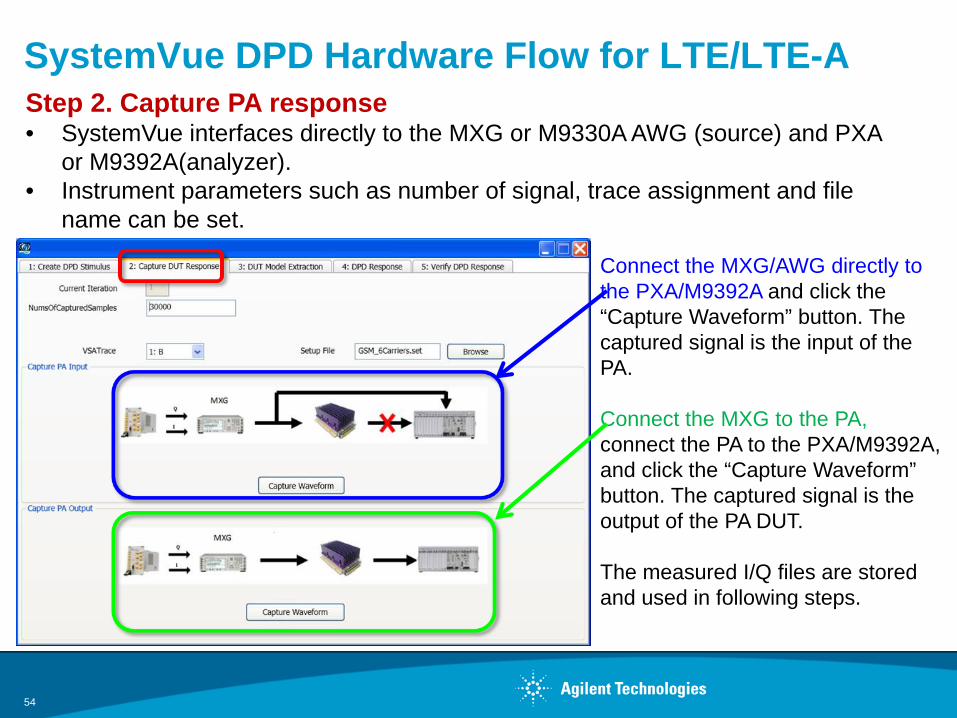
Connect the MXG/AWG directly to the PXA/M9392A and click the “Capture Waveform” button. The captured signal is the input of the PA.
Connect the MXG to the PA, connect the PA to the PXA/M9392A, and click the “Capture Waveform” button. The captured signal is the output of the PA DUT.
The measured I/Q files are stored and used in following steps.
54
Step 2. Capture PA response• SystemVue interfaces directly to the MXG or M9330A AWG (source) and PXA
or M9392A(analyzer).• Instrument parameters such as number of signal, trace assignment and file
name can be set.
SystemVue DPD Hardware Flow for LTE/LTE-A
DPD AM-to-AM Characteristic
55
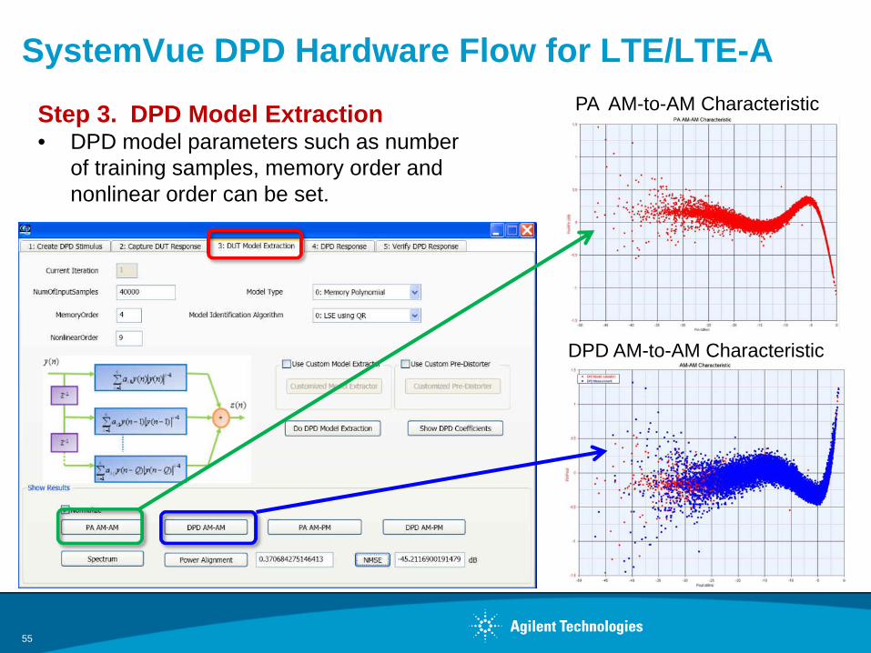
SystemVue DPD Hardware Flow for LTE/LTE-A
Step 3. DPD Model Extraction• DPD model parameters such as number
of training samples, memory order and nonlinear order can be set.
PA AM-to-AM Characteristic
56
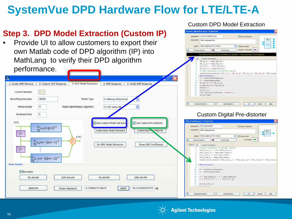
SystemVue DPD Hardware Flow for LTE/LTE-A
Step 3. DPD Model Extraction (Custom IP)• Provide UI to allow customers to export their
own Matlab code of DPD algorithm (IP) into MathLang to verify their DPD algorithm performance.
Custom DPD Model Extraction
Custom Digital Pre-distorter
57
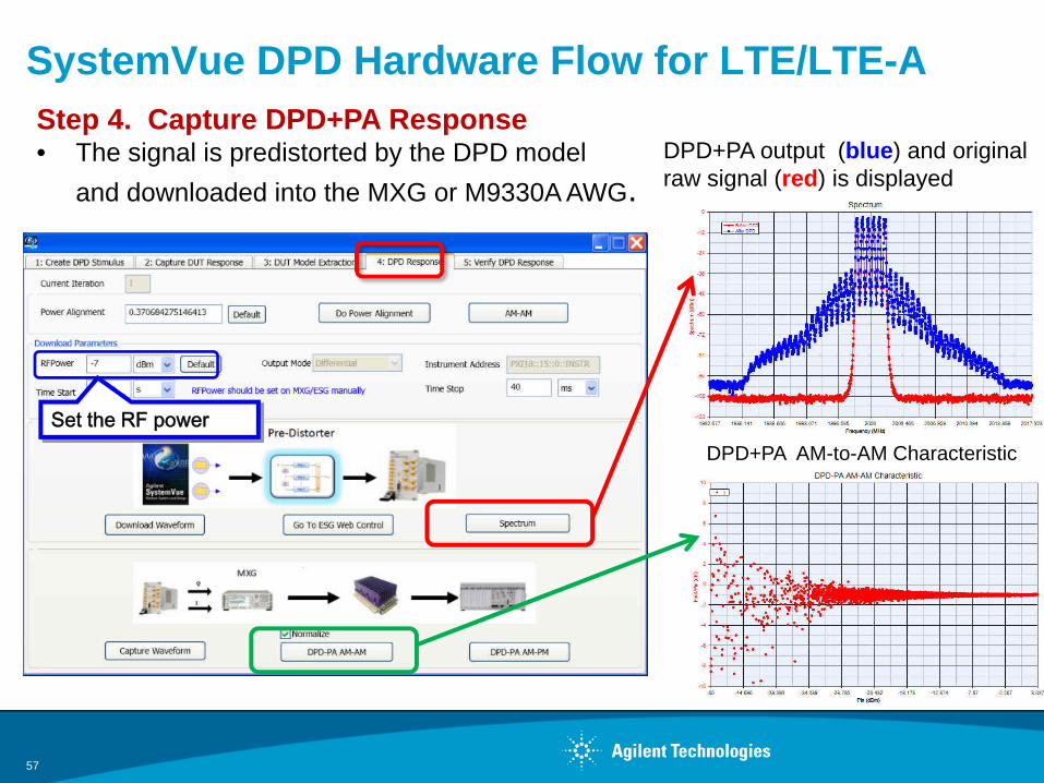
SystemVue DPD Hardware Flow for LTE/LTE-AStep 4. Capture DPD+PA Response• The signal is predistorted by the DPD model
and downloaded into the MXG or M9330A AWG.DPD+PA output (blue) and original raw signal (red) is displayed
Set the RF powerDPD+PA AM-to-AM Characteristic
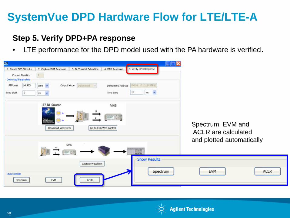
SystemVue DPD Hardware Flow for LTE/LTE-A
Step 5. Verify DPD+PA response• LTE performance for the DPD model used with the PA hardware is verified.
Spectrum, EVM andACLR are calculatedand plotted automatically
58
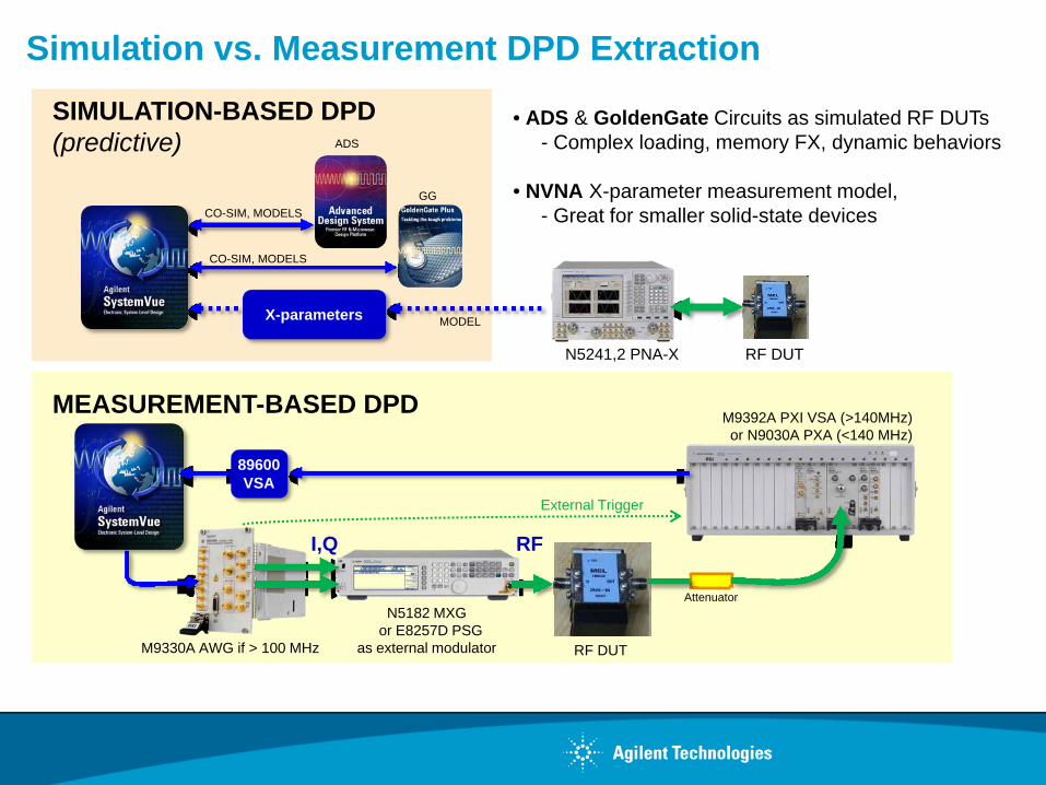
Simulation vs. Measurement DPD Extraction
External Trigger
Attenuator N5182 MXG
or E8257D PSGas external modulatorM9330A AWG if > 100 MHz
89600VSA
M9392A PXI VSA (>140MHz)or N9030A PXA (<140 MHz)
I,Q RF
RF DUT
SIMULATION-BASED DPD(predictive)
• ADS & GoldenGate Circuits as simulated RF DUTs- Complex loading, memory FX, dynamic behaviors
• NVNA X-parameter measurement model,- Great for smaller solid-state devices
X-parameters
RF DUTN5241,2 PNA-X
MEASUREMENT-BASED DPD
CO-SIM, MODELS
CO-SIM, MODELS
MODEL
ADS
GG
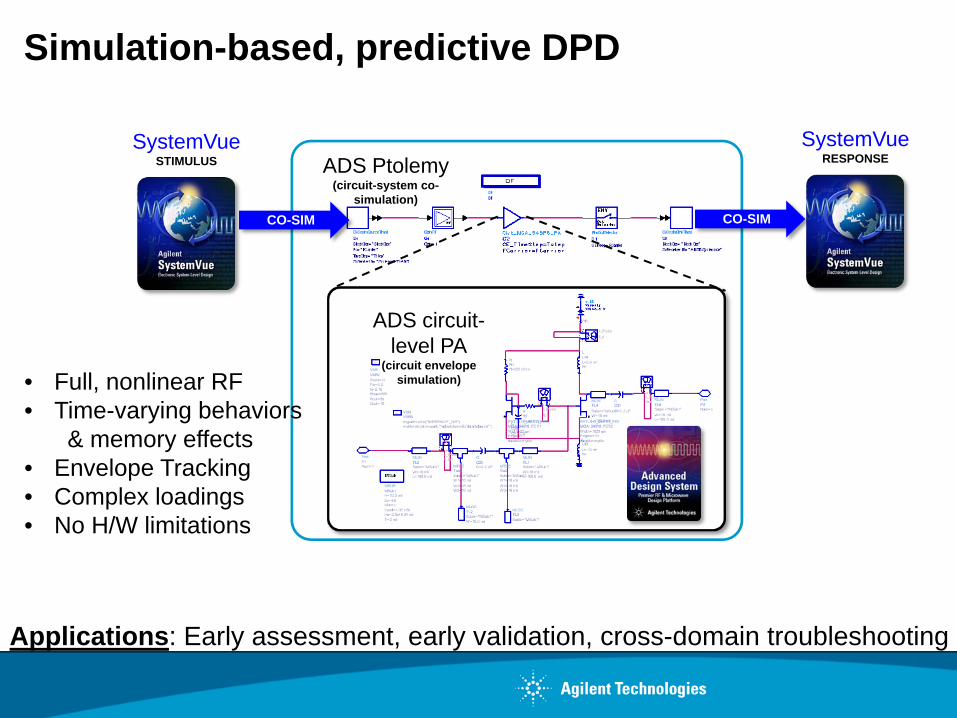
Simulation-based, predictive DPD
ADS circuit-level PA
(circuit envelope simulation)
ADS Ptolemy(circuit-system co-
simulation)
SystemVueSTIMULUS
SystemVueRESPONSE
CO-SIM
• Full, nonlinear RF• Time-varying behaviors
& memory effects• Envelope Tracking• Complex loadings• No H/W limitations
CO-SIM
Applications: Early assessment, early validation, cross-domain troubleshooting
Conclusion
New bandwidth and linearity requirements are driving 4G designers to spec DPD earlier in their system designs
The velocity of the industry is pushing DPD activity in-house, where designers are taking a more active role
The integration of an open Comms EDA environment with versatile wideband instruments enables
– Flexibility for modeling, realization, validation, and troubleshooting– Higher performance– Integration with the baseband DSP you are already doing
Further information
About Wideband DPD – Watch a demo:
http://www.youtube.com/watch?v=bocF6P74T9E– Read an app note:
http://cp.literature.agilent.com/litweb/pdf/5990-8883EN.pdf
About Agilent Products – http://www.agilent.com/find/eesof-systemvue– http://www.agilent.com/find/modular
Contact– Stephen Slater ([email protected])
– Jake Sanderson ( [email protected])

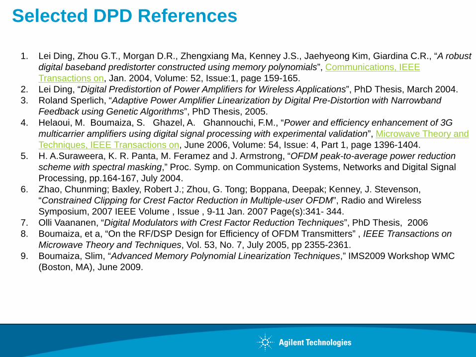
1. Lei Ding, Zhou G.T., Morgan D.R., Zhengxiang Ma, Kenney J.S., Jaehyeong Kim, Giardina C.R., “A robust digital baseband predistorter constructed using memory polynomials”, Communications, IEEE Transactions on, Jan. 2004, Volume: 52, Issue:1, page 159-165.
2. Lei Ding, “Digital Predistortion of Power Amplifiers for Wireless Applications”, PhD Thesis, March 2004.3. Roland Sperlich, “Adaptive Power Amplifier Linearization by Digital Pre-Distortion with Narrowband
Feedback using Genetic Algorithms”, PhD Thesis, 2005.4. Helaoui, M. Boumaiza, S. Ghazel, A. Ghannouchi, F.M., “Power and efficiency enhancement of 3G
multicarrier amplifiers using digital signal processing with experimental validation”, Microwave Theory and Techniques, IEEE Transactions on, June 2006, Volume: 54, Issue: 4, Part 1, page 1396-1404.
5. H. A.Suraweera, K. R. Panta, M. Feramez and J. Armstrong, “OFDM peak-to-average power reduction scheme with spectral masking,” Proc. Symp. on Communication Systems, Networks and Digital Signal Processing, pp.164-167, July 2004.
6. Zhao, Chunming; Baxley, Robert J.; Zhou, G. Tong; Boppana, Deepak; Kenney, J. Stevenson, “Constrained Clipping for Crest Factor Reduction in Multiple-user OFDM”, Radio and Wireless Symposium, 2007 IEEE Volume , Issue , 9-11 Jan. 2007 Page(s):341- 344.
7. Olli Vaananen, “Digital Modulators with Crest Factor Reduction Techniques”, PhD Thesis, 2006 8. Boumaiza, et a, “On the RF/DSP Design for Efficiency of OFDM Transmitters” , IEEE Transactions on
Microwave Theory and Techniques, Vol. 53, No. 7, July 2005, pp 2355-2361.9. Boumaiza, Slim, “Advanced Memory Polynomial Linearization Techniques,” IMS2009 Workshop WMC
(Boston, MA), June 2009.
Selected DPD References
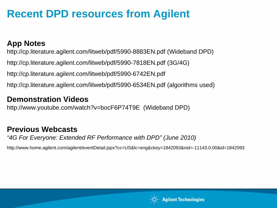
Recent DPD resources from Agilent
App Notes http://cp.literature.agilent.com/litweb/pdf/5990-8883EN.pdf (Wideband DPD)
http://cp.literature.agilent.com/litweb/pdf/5990-7818EN.pdf (3G/4G)
http://cp.literature.agilent.com/litweb/pdf/5990-6742EN.pdf
http://cp.literature.agilent.com/litweb/pdf/5990-6534EN.pdf (algorithms used)
Demonstration Videoshttp://www.youtube.com/watch?v=bocF6P74T9E (Wideband DPD)
Previous Webcasts“4G For Everyone: Extended RF Performance with DPD” (June 2010)http://www.home.agilent.com/agilent/eventDetail.jspx?cc=US&lc=eng&ckey=1842093&nid=-11143.0.00&id=1842093


![Mobile and Wireless Technologies on Sphygmomanometers and … · 2. GSM Module [18]: includes Baseband part and RF part. The main components are Baseband IC (including DSP), TFT-LCD,](https://img.pdfslide.net/doc/110x75/5f663692836b486a4603428a/mobile-and-wireless-technologies-on-sphygmomanometers-and-2-gsm-module-18-includes.jpg)