Embed Size (px)
Citation preview

Weidong Chen 1. Institute of High Energy Physics, CAS China 2. Dongguan Neutron Science Center, Dongguan China
Sep.13th, 2016, The 5th NIBS @ Oxford.
RF H-Minus Ion Source Development in China Spallation Neutron Source
1

Outline of this talk
2
Introduction to China Spallation neutron source (CSNS) and current penning-SPS
The designed structure of CSNS-RF ion source Summary

3
Introduction to CSNS
Project Phase I II
Beam Power on target [kW] 100 500
Proton energy [GeV] 1.6 1.6
Average beam current [μA] 62.5 312.5
Pulse repetition rate [Hz] 25 25
Linac energy [MeV] 80 250
Linac type DTL +Spoke
Linac RF frequency [MHz] 324 324
Macropulse. ave current [mA]
15 40
Macropulse duty factor 1.0 1.7
Target Material Tungsten Tungsten
The first section of DTL was successfully tested. 18 mA 20Mev H-Minus beam are successfully accelerated, and collected by dumper. The other three sections of DTL are under installation.
18 mA 20Mev

4
Introduction to CSNS
Photo taken on November of 2015
Most of the facility is located 10 meters under ground.

Current H-Minus source in service
5
Peak: 65mA, Width: 500us, Repeat: 25Hz, Life: weeks RMS Emittance: around 0.8π •mm•mrad. 25 mA is within RFQ acceptance, 0.2π •mm•mrad

6
Integrated penning magnet Independent penning magnet. Change the extraction voltage freely.
Connect a resister in extractor PS, to limit the current when spark happens.
Increase the overlap of the ceramic HV break, make the -50kV platform more stable.
Put extraction power supply closer to the source, to decrease the induced voltage when it is pulsed on and off.
Major activity of current source

7
High H-Minus current up to 70 mA or more. Easy to change and maintain.
Current H-Minus source in service
Cesium is hard to deal with. Too few Cs will limit the production of the H-Minus beam, while too much Cs makes the extraction HV not stable. Life time is limited by the Cs sputtering. Beam emittance is high because of the hot DC-discharge.
Advantages:
Disadvantages:

8
Amplifier
Since the impedance and matching-frequency changes slightly before and after ignition. We aim to minimize the reflection of the RF power by change the waveform of input signal. The waveform is programmed with 1000000 dots, which aims to smoothly ramp the frequency within one pulse.
Matching network is similar to SNS source. The insulation transformer and impedance transformer are separated. The solid state amplifier produce 80kW power on maximum.

Layout of the system
9

RF-ion source
10
The design is similar to SNS, J-PARC, DESY RF ion sources, with modifications in several aspects.

The plasma chamber and antenna
11
Al2O3 AlN Si3N4
Thermal Conductivity (W/mK) 16~27 70~150 16~90 (60)
Thermal Expansion (ppm/K) ~7 ~4.6 ~2.8
Flexural strength (MPa) ~350 ~300 ~900
Vicker Hardness (GPa) ~16 ~11 ~14
Heat shock resistance (Cesius) ~200 ~400 ~800
Flexural strength
Copper Antenna and SS cooling pipe are brazed on outer wall, advantages: 1. For heat transfer 2. Closer to plasma, higher power
efficiency. 3. Cusp magnet is closer to chamber.
Requirement of B field strength of NbFeB magnet is lower.
Epoxy filled in vacuum.

12
From the estimation, the typical mean free path of H- ions in plasma is around 0.5~2cm (depends on pressure— 6~20 mTorr, RF power—20~60 kW and confining condition).H2* have a mean free path of same order.
Size of plasma chamber and cusp magnets
The H- ions produced 3 cm away seems very hard to reach extraction port. So we set the chamber inner diameter to 6.7 cm (3+0.7+3). The cusp magnet length is 7.5cm. Technically, it is hard to make B value homogeneous along the magnet surface if the magnet is too long.

13
The plasma chamber and antenna
The cooling parts are either made of either segmented copper block or SS-tube to minimize the induced electromagnetic field and eddy current.
Thermal Design Power: 2000W@25Hz, 2.5%D.F., 80kW pulse
Simulation of the induced EM field.
The induced current will counter act the EM field produced by antenna

14
The plasma chamber and antenna
Thermal simulation of the chamber@ 1500W, suppose a 4π-homogenous radiation of the plasma. Maximum temperature of the chamber is 81 degree.
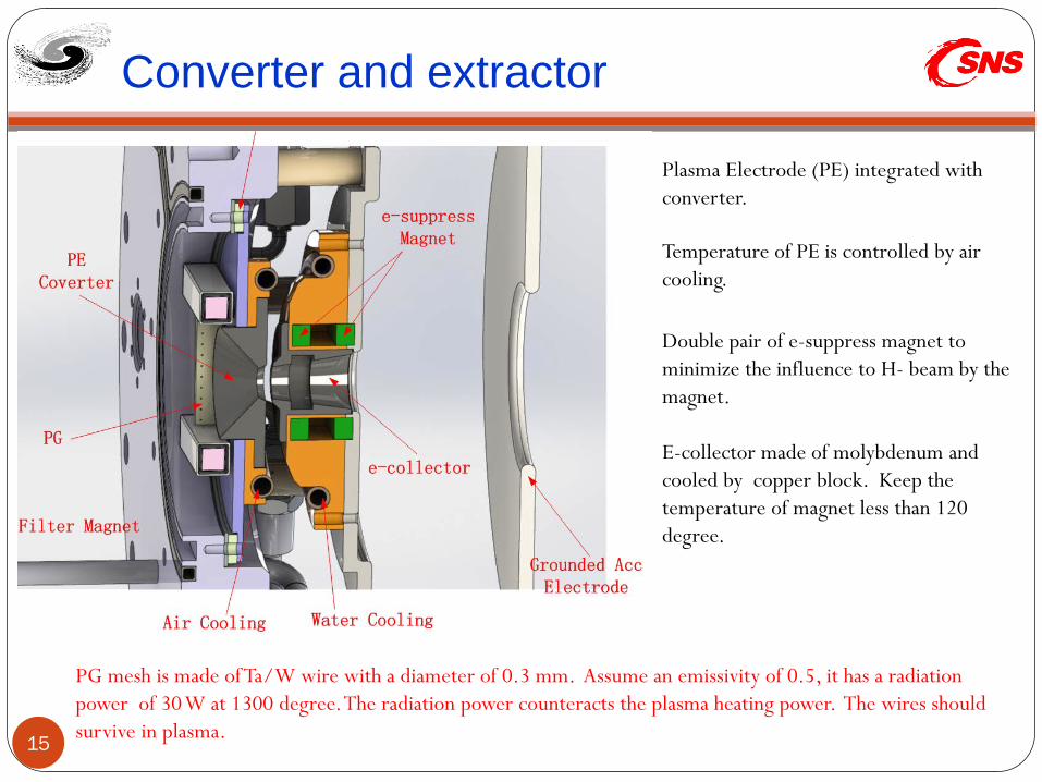
Converter and extractor
15
Plasma Electrode (PE) integrated with converter.
Temperature of PE is controlled by air cooling.
Double pair of e-suppress magnet to minimize the influence to H- beam by the magnet. E-collector made of molybdenum and cooled by copper block. Keep the temperature of magnet less than 120 degree.
PG mesh is made of Ta/W wire with a diameter of 0.3 mm. Assume an emissivity of 0.5, it has a radiation power of 30 W at 1300 degree. The radiation power counteracts the plasma heating power. The wires should survive in plasma.

16
Converter and extractor
Simulation with 0.8 A electron beam, with initial temperature of 5eV. All of the electrons are collected
Simulation with 40 mA H- beam, with initial temperature of 5eV. 100% transmission. Normalized emittance at acceleration electrode: 0.071 π •mm•mrad

Self-cleaning of the chamber
17
Area of stainless steel exposed to plasma is minimized to reduce the sputtering and degassing. Instead Mo, Pt coating and Ta material are used to face the plasma.
150eV H He Ar
Ti 0 0.0471 0.259
Fe 0 0.0705 0.611
Mo 0 0 0.442
Ta 0 0 0.379
Pt 0 0 0.603
Possible contaminant on converter surface. • CsOH—Melting at 272 degree. • Metal oxides— Bombardment with helium ions • Organic molecules is easy to sputter with protons
and helium ions.
Most of the ions in plasma has an energy less than 150 eV. Sputtering rate of ions on metal surface.
He and H2 have similar Paschen curve. If converter is contaminated, we will try to clean it with He plasma, then re-cesiation. Try to make it maintain-free.

18
Trigger System Pulsed discharge, chamber is negatively biased. <100mA, <800 V, 2 ms pulse width 1.5~4W mean power, special cooling is not needed.
Chamber length 1.8 cm Working pressure:1.2~3.9 Torr Break down voltage: 400~800V
Working pressure of the RF plasma chamber: 6~20 mTorr. The size of the holes should be determined by simulation and experiment.

19
Cusp magnet
From the center of the chamber.
Since the antenna is brazed on the ceramic chamber, this save same distance to put the cusp magnet closer to center. 4500 Gauss on magnet surface can produce 360 Gauss at the inner wall of the chamber. B free area (B<20 G) is 22 mm from center.
From J-PARC’s publication, axial magnetic field of proper value can enhance the H- beam production. This can also be tried in our design, as an optional.
Cusp magnet have a length of 7.5 cm.

Summary
20
Penning-SPS is in service, several improvements are made. RF source is also under development. Si3N4 ceramic is used,
and antenna is brazed on ceramic chamber. PG is put in to plasma to optimize the H- production. Sputter free material is used to face the plasma. We are try to
make a self-clean, maintain free machine.

21
The performance is finished.
Questions and suggestions are welcome!