Embed Size (px)
Citation preview
ORIGINAL CONTRIBUTION
Ring VCO Design with Variable Capacitance XNOR Delay Cell
Manoj Kumar • Sandeep Arya • Sujata Pandey
Received: 11 March 2013 / Accepted: 22 August 2014 / Published online: 18 September 2014
� The Institution of Engineers (India) 2014
Abstract This paper presents the new designs of voltage
controlled oscillator (VCO) with three transistors XNOR
gate as variable capacitive load. Design of three, five and
seven stage VCO have been reported using single ended
ring topology. CMOS inverter based delay cell is modified
with addition of XNOR capacitive load. Output frequency
has been controlled by applied voltage to variable capaci-
tive load. Control voltage of VCO has been varied from 1.3
to 2.1 V. Three stage VCO provides output frequency
variation in the range of 3.52–3.34 GHz with power con-
sumption variation from 0.81 to 1.76 mW. Five stage VCO
shows frequency variation from 2.06 to 1.98 GHz with
power consumption varying from 1.35 to 2.94 mW.
Moreover, frequency of seven stage VCO varies from 1.47
to 1.41 GHz with varying power from 1.89 to 4.12 mW.
Power consumption and output frequency of proposed
VCO circuits have been compared with earlier reported
circuits and present approach shows considerable
improvements.
Keywords CMOS � Delay cell � Power consumption �Variable capacitance � Voltage controlled oscillator (VCO)
Introduction
In modern high performance communication systems phase
locked loop (PLL) is the commonly used circuit component
having wide application in frequency synthesis, clock and
data recovery circuits [1–3]. Clock is generated by analog
circuits called PLL which contains a phase detector, a
charge pump, a loop filter and voltage controlled oscillator
(VCO). VCO is the core block of these RF systems.
A VCO can be built using ring structures, relaxation cir-
cuits, or inductor–capacitor (LC) resonant circuits [3–5].
The LC based design has the best noise and frequency
performance due to the high quality factor. Disadvantage of
LC based design is that the combination of inductor (L) and
capacitor (C) consumes large area on integrated circuit. On
other side design of CMOS based ring VCO is straight-
forward and provides multiple frequency components with
wide tuning range [6]. CMOS is the most favored tech-
nology meeting demands such as high data rates, high
packaging density, global mobility and wide communica-
tion service coverage. Due to flexibility of on chip inte-
gration, CMOS based ring oscillators have become
essential building blocks in various communication sys-
tems. Shortcoming of ring based oscillators includes large
power consumption, phase noise problems and the limit of
highest achievable frequency. In recent years power con-
sumption has become major challenge for wireless com-
munication systems. Growing demand of portable devices
like cellular phones, notebooks, personal communication
devices have further accelerated the need of power saving.
Power dissipation in CMOS systems can be divided into
two broad categories: static power and dynamic power
dissipation. Dynamic power is important during the normal
operation time especially at high frequency operation.
Static power is more important in standby operation
M. Kumar (&)
University School of Information and Communication
Technology, Guru Gobind Singh Indraprastha University,
New Delhi, India
e-mail: [email protected]
S. Arya
Department of Electronics and Communication Engineering,
Guru Jambheshwar University of Science and Technology,
Hisar, India
S. Pandey
Department of Electronics and Communication Engineering,
Amity University, Noida, India
123
J. Inst. Eng. India Ser. B (October–Decmber 2015) 96(4):371–379
DOI 10.1007/s40031-014-0154-4
especially in battery powered systems. Total power con-
sumption in CMOS circuit is given as:
Ptotal ¼ aCLV2ddf þ IscVdd þ IsubVdd þ Igatel leakageVdd ð1Þ
In Eq. (1), a is the switching activity; CL is the capacitance
of the load; f is the clock frequency; and Vdd is the supply
voltage. The first two components represent the dynamic
power consumption and remaining two components shows
static power consumption.
Power consumption is becoming central design criteria
for VLSI circuits used in communication and mobile sys-
tems. VCO being the major component of communication
system, is also responsible for most of the power con-
sumption. In modern VCO designs power consumption and
output frequency range are important performance metrics
[7–12]. A ring oscillator has number of delay stages, with
output of last stage fed back to input of the first stage.
A VCO block diagram having single ended N-delay stages
is shown in Fig. 1.
The ring structure in VCO must provide a phase shift of
2p and unity voltage gain for oscillation occurrence. Each
delay cell also provides a phase shift of p/N, where N
represents the total number of delay stages. The remaining
p phase shift is provided with dc inversion introduced by
the inverter delay cells. For single ended oscillator design
the odd numbers of delay stages must be used for dc
inversion. Frequency of oscillation of VCO having N-sin-
gle ended delay stage is given by fo ¼ 12Ntd
; where N is the
number of delay stages and td is delay of each stage [8, 13].
Design of delay stage is major challenge in VCO circuit
and superior design of these delay cells improves the
overall performance. A variety of delay cells have been
reported in literature for VCO design including multiple-
feedback loops, dual-delay paths and single ended delays.
These delay cells have been implemented by various
approach like conventional inverter stages, latches, cross
coupled cells etc. [14–18].
In present work new VCO circuits using three transistors
XNOR as variable capacitance load have been reported
with reduced power consumption and wide frequency
range. CMOS inverter delay cell has been improved with
addition of XNOR load and the frequency has been con-
trolled by tuning the variable capacitance of XNOR.
System Description
Oscillators implemented in present work are based on
single ended ring topology with odd number of delay ele-
ments. Three, five and seven stages VCO circuits have
been designed using variable capacitance approach. A three
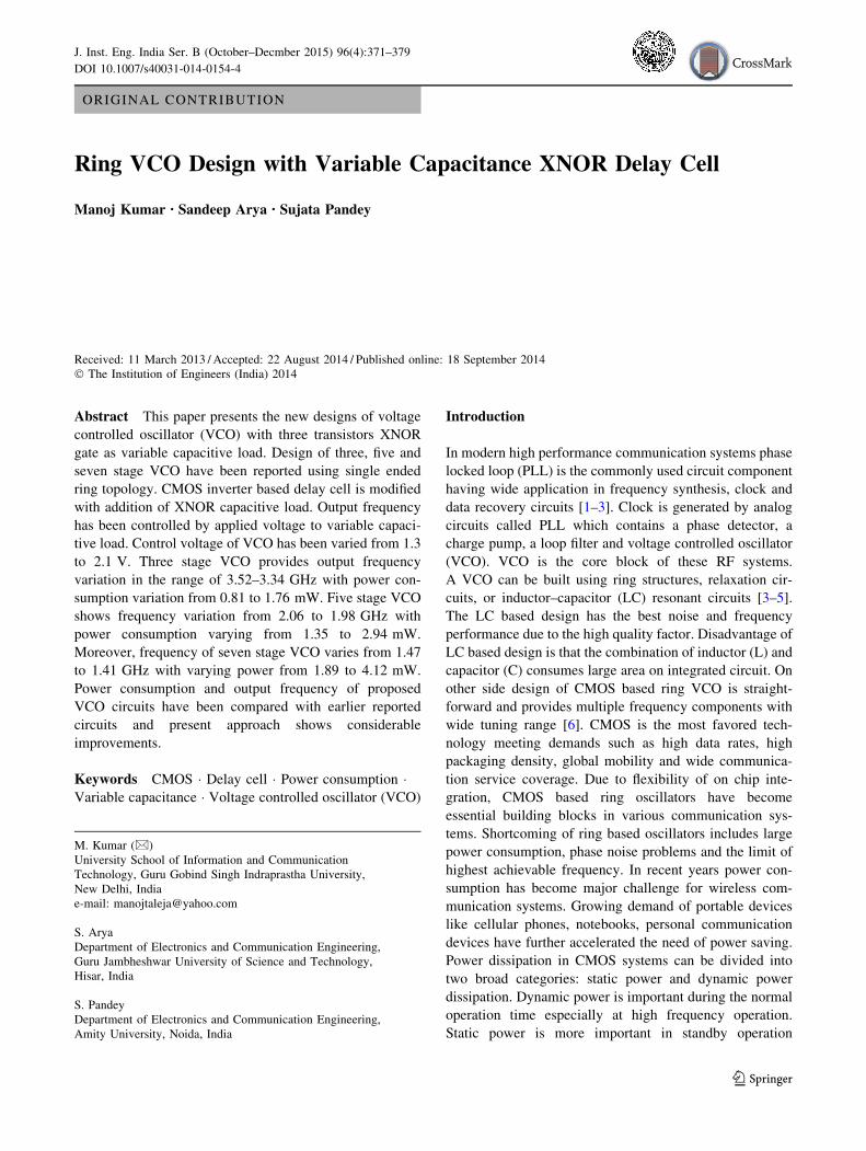
transistors XNOR gate, as shown in Fig. 2, has been used
as variable capacitive loading in ring structure. In this
XNOR, gate length of all three transistors have been taken
as 0.18 lm. Widths (Wn) of NMOS transistors N1 and N2
have been taken 2.5 and 0.5 lm, respectively. Width (Wp)
for transistor P1 has been taken as 1 lm.
In XNOR circuit when A = 0 and B = 0 output is high
as P1 transistor is in on condition and N1, N2 are in off
condition. With input combination of A = 0 and B = 1
circuit shows low output as transistor P1 is off and output
node is discharged by transistor N2. In another case when
A = 1 and B = 0 both transistors are in on condition and
output node is discharged rapidly by N1 and N2 transistors.
In this case with A = 1 transistor N1 turns on which further
turn on the transistor N2 and a low resistance path is pro-
vided by N1 and N2. For acceptable output logic level for
certain input combinations (W/L) ratios have been sized.
Width of N1 has been made large to reduce resistance in
the discharging path. The voltage degradation due to
threshold drop can be reduced by increasing W/L ratio of
transistor of N1. The following equation [19] relates the
threshold voltage with cannel length and width of MOS
transistor.
Controllable delay cell
Controllable delay cell
Controllable delay cell
Fig. 1 Block diagram of single
ended VCO
VDD
B
A
XNORP1
N1
N2
Fig. 2 Three transistor XNOR gate
372 J. Inst. Eng. India Ser. B (October–Decmber 2015) 96(4):371–379
123

VT ¼ VT0 þ cffiffiffiffiffiffiffiffiffiffiffiffiffiffiffiffiffiffi
VSB þ u0
p
� �
� altox
LVSB þ u0ð Þ
� avtox
LVds þ aw
tox
WVSB þ u0ð Þ ð2Þ
where Vt0 is the zero bias threshold voltage; c is bulk
threshold coefficient; u0 is 2uF and uF is Fermi potential;
tox is the thickness of oxide; and al, av and aw are the
process dependent parameters. From (2) it is apparent that
by increasing the W, it is possible to reduce the voltage
degradation. In last case, when A = 1 and B = 1, output
node shows high logic as transistor N1 is on and high logic
is passed to output, so circuit works as XNOR gate.
Proposed delay cell have a CMOS inverter and a XNOR
gate as shown in Fig. 3a. For inverter section width of
PMOS transistor (P2) is taken as 1.0 lm whereas as width
for NMOS transistor (N3) is taken as 0.5 lm. CMOS
inverter delay cell has been modified with addition of con-
trolled variable capacitive load. Gate to channel capacitance
of MOS transistor contribute to total gate capacitance.
Therefore total output capacitance of delay cell varies with
the application of control voltage which further modulates
the propagation delay of individual stage. Here, in Fig. 3a
the total gate to source/drain capacitance of transistors N1
shows variation with applied control voltage (Vc). The total
capacitance at node CL depends on the gate capacitance of
N1 which further depends on value of control voltage (Vc).
Equivalent circuit of proposed delay cell has been shown in
Fig. 3b. CI is the initial capacitance and DC is the change is
capacitance with applied control voltage (Vc). Capacitance
is dependent on external bias voltage applied across the pn
junction in MOS transistors. Equivalent capacitance (Ceq) is
related with voltage difference as shown in Eq. (3), whereCj
is the junction capacitance.
Ceq ¼DQDV
¼ 1
V2 � V1
Z
CjdV ð3Þ
With application of Vc transistor P1 is in off and tran-
sistor N1 is in on condition. With increase in voltage at the
gate of transistor P1 the Ceq increases as given in Eq. (3).
Difference between gate and drain/source voltage of P1
decreases which increases the Ceq. Further, for transistor
N1 the difference of gate and drain/source voltage is
reduced with applied control voltage (Vc). This difference
is further reduced with increase in Vc and Ceq of transistor
N1 is increased. As the width of transistor N1 is highest
among the three transistors, therefore it contributes more in
total load capacitance CL. For transistor N2 the difference
of gate voltage and drain/source voltage is also reduced
with application of more control voltage and Ceq of tran-
sistor N2 also increases. As the width of N2 is smallest
among three transistors so it contributes less towards total
load capacitance (CL). Due to increase in load capacitance
with changing control voltage, the propagation delay of
proposed delay cell is increased. Delay increases with
change in control voltage and subsequently the output
frequency shows downward trend. Power consumption
shows upward trend as transistor N1 is in on condition and
provides the path for current conduction to ground.
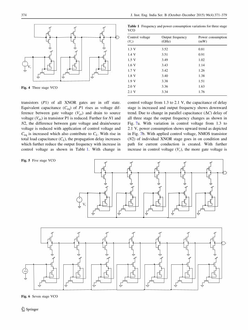
Three, five and seven stages VCO based on ring topology
using XNOR gate capacitive loading has been shown in
Figs. 4, 5 and 6. Control voltage (Vc) has been varied from1.3
to 2.1 V for obtaining the different frequency components.
Results and Discussions
Simulations have been carried out using SPICE based on
TSMC 0.18 lm CMOS process technology. Table 1 shows
the output frequency and power consumption results for
three stage VCO. With applied control voltage, all three
stage shows variation in load capacitance (CL). PMOS
a b
OutIn
Vc
CiΔC
CL
Vc
InOutCL
P2
P1
N2
N1
N3
Fig. 3 a Delay cell with
variable capacitance.
b Equivalent circuit
J. Inst. Eng. India Ser. B (October–Decmber 2015) 96(4):371–379 373
123
transistors (P1) of all XNOR gates are in off state.
Equivalent capacitance (Ceq) of P1 rises as voltage dif-
ference between gate voltage (Vgs) and drain to source
voltage (Vds) in transistor P1 is reduced. Further for N1 and
N2, the difference between gate voltage and drain/source
voltage is reduced with application of control voltage and
Ceq is increased which also contribute to CL. With rise in
total load capacitance (CL), the propagation delay increases
which further reduce the output frequency with increase in
control voltage as shown in Table 1. With change in
control voltage from 1.3 to 2.1 V, the capacitance of delay
stage is increased and output frequency shows downward
trend. Due to change in parallel capacitance (DC) delay of
all three stage the output frequency changes as shown in
Fig. 7a. With variation in control voltage from 1.3 to
2.1 V, power consumption shows upward trend as depicted
in Fig. 7b. With applied control voltage, NMOS transistor
(N2) of individual XNOR stage goes in on condition and
path for current conduction is created. With further
increase in control voltage (Vc), the more gate voltage is
Vc
Fig. 4 Three stage VCO
Vc
Fig. 5 Five stage VCO
Table 1 Frequency and power consumption variations for three stage
VCO
Control voltage
(Vc)
Output frequency
(GHz)
Power consumption
(mW)
1.3 V 3.52 0.81
1.4 V 3.51 0.91
1.5 V 3.49 1.02
1.6 V 3.43 1.14
1.7 V 3.42 1.26
1.8 V 3.40 1.38
1.9 V 3.38 1.51
2.0 V 3.36 1.63
2.1 V 3.34 1.76
V=0
Fig. 6 Seven stage VCO
374 J. Inst. Eng. India Ser. B (October–Decmber 2015) 96(4):371–379
123

applied at gate of N2, higher drain/source currents gives
more power consumption. The variation of output fre-
quency with power consumption is shown in Fig. 8.
Table 2 shows the results for five stage VCO designed
with proposed delay cell. Output frequency shows down-
ward trend with change in control voltage from 1.3 to
2.1 V. Output frequency is reduced because with increase
in Vc, the capacitance of individual stage is increased.
Frequency variation with control voltage has been shown
in Fig. 9a. Here, the power consumption of individual
stages rises with application of more control voltage (Vc),
which further increases the total power consumption of
circuit. Power consumption variations with Vc has been
shown in Fig. 9b. Power consumption against output fre-
quency graph for five stage VCO is shown in Fig. 10.
Table 3 shows the results for seven stage VCO. Output
frequency and power consumption variation has been
shown in Fig. 11a, b. Power consumption variation with
output frequency has been shown in Fig. 12.
Output waveforms for three, five and seven stages VCO
with control voltage of 1.3 V have been shown in Fig. 13a–
c respectively. Further the waveform results for control
voltage of 2.1 V for three, five and seven stages VCO have
been shown in Fig. 14a–c.
a b
3.3
3.35
3.4
3.45
3.5
3.55
1.2 1.4 1.6 1.8 2 2.2
Control Voltage, V
Out
put F
requ
ency
, GH
z
00.20.40.60.8
11.21.41.61.8
2
1.2 1.4 1.6 1.8 2 2.2
Control Voltage, V
Pow
er C
onsu
mpt
ion,
mW
Fig. 7 a Output frequency, b power consumption for three stage VCO
Table 2 Frequency and power consumption variations for five stage
VCO
Control voltage
(Vc)
Output frequency
(GHz)
Power consumption
(mW)
1.3 V 2.06 1.35
1.4 V 2.05 1.52
1.5 V 2.04 1.71
1.6 V 2.03 1.90
1.7 V 2.03 2.10
1.8 V 2.01 2.31
1.9 V 1.99 2.51
2.0 V 1.98 2.73
2.1 V 1.98 2.94
00.20.40.60.8
11.21.41.61.8
2
3.3 3.35 3.4 3.45 3.5 3.55
Power Consumption, mW
Out
put F
requ
ency
, GH
z
Fig. 8 Power consumption against output frequency for three stage
VCO
a b
1.971.981.99
22.012.022.032.042.052.062.07
1.2 1.4 1.6 1.8 2 2.2Control voltage (V)
Out
put F
requ
ency
, GH
z
0
0.51
1.52
2.53
3.5
1.2 1.4 1.6 1.8 2 2.2Control voltage, V
Pow
er C
onsu
mpt
ion,
mW
Fig. 9 a Output frequency, b power consumption for five stage VCO
J. Inst. Eng. India Ser. B (October–Decmber 2015) 96(4):371–379 375
123

In reported circuits, power consumption is increasing
with increase in number of delay stages, whereas output
frequency is showing downward trend. Number of stages
may be decreased or increased depending upon the appli-
cation, requirement for frequency range and power con-
sumption. Design reported here are improved than designs
as compared to conventional NAND and NOR based var-
iable capacitive load as two input gate require four tran-
sistor whereas in present approach variable capacitive load
require only three transistor. A comparison with earlier
reported circuits in terms of power consumption and output
frequency range is given in Table 4. Proposed circuit’s
shows better performance in terms of power consumption
and output frequency range.
Conclusions
Voltage controlled oscillators with three transistor XNOR
gate as variable capacitive loading have been presented. A
new delay cells have been proposed using XNOR gate and
CMOS inverter. Three, five and seven stages VCO circuits
using proposed delay cell have been simulated with SPICE
simulator. Three stage VCO shows output frequency from
3.52 to 3.34 GHz with power consumption variations from
0.81 to 1.76 mW. Five stage VCO gives the output fre-
quency in the range of 2.06 to 1.98 GHz and power con-
sumption in the range of 1.35 to 2.94 mW. Further, seven
stage VCO depicts the output frequency from 1.47 to
1.41 GHz with power consumption variation from 1.89 to
4.12 mW. Reported circuits have advantage of low power
consumption and wide output frequency range with
1.971.981.99
22.012.022.032.042.052.062.07
1 1.5 2 2.5 3
Power Consumption, mW
Out
put F
requ
ency
,GH
z
Fig. 10 Power consumption against output frequency variation for
five stage VCO
Table 3 Frequency and power consumption variations for seven
stage VCO
Control voltage
(Vc)
Output frequency
(GHz)
Power consumption
(mW)
1.3 V 1.47 1.89
1.4 V 1.46 2.14
1.5 V 1.46 2.40
1.6 V 1.45 2.67
1.7 V 1.44 2.94
1.8 V 1.44 3.23
1.9 V 1.43 3.52
2.0 V 1.42 3.82
2.1 V 1.41 4.12
1.41
1.42
1.43
1.44
1.45
1.46
1.47
1.48
1.7 2.2 2.7 3.2 3.7 4.2 4.7Power Consumption, mW
Out
put F
requ
ency
, G
Hz
Fig. 12 Power consumption against output frequency variation for
seven stage VCO
a b
1.41
1.42
1.43
1.44
1.45
1.46
1.47
1.48
1.2 1.4 1.6 1.8 2 2.2Control Voltage, V
Out
put F
requ
ency
, GH
z
00.5
11.5
22.5
33.5
44.5
1.2 1.4 1.6 1.8 2 2.2Control Voltage, V
Pow
er C
onsu
mpt
ion,
mW
Fig. 11 a Output frequency, b power consumption for seven stage VCO
376 J. Inst. Eng. India Ser. B (October–Decmber 2015) 96(4):371–379
123

Fig. 13 VCO waveforms at control voltage of 1.3 V for a three stage, b five stage, c seven stage
J. Inst. Eng. India Ser. B (October–Decmber 2015) 96(4):371–379 377
123
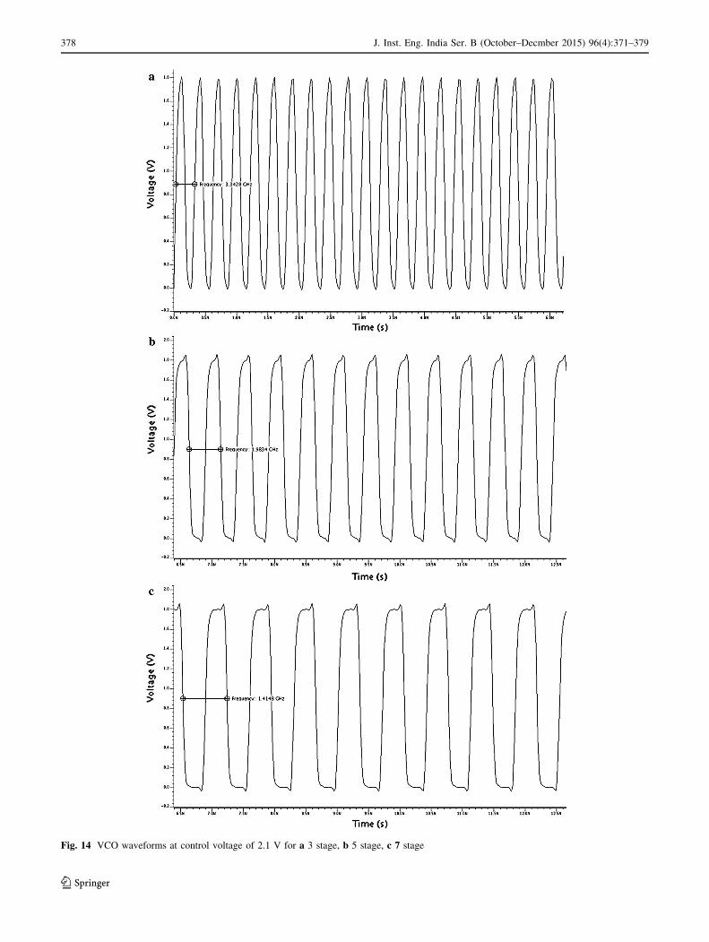
Fig. 14 VCO waveforms at control voltage of 2.1 V for a 3 stage, b 5 stage, c 7 stage
378 J. Inst. Eng. India Ser. B (October–Decmber 2015) 96(4):371–379
123
reduced transistor count. Output frequency and power
consumption results have been compared with earlier
reported circuits and proposed circuit shows significant
improvements.
References
1. T.-Y. Hsu, C.C. Wang, C.-Y. Lee, Design and analysis of a
portable high-speed clock generator. IEEE Trans. Circuits Syst. II
48, 367–375 (2001)
2. J.-H. Tsai, J.-P. Chou, A K-band low-power CMOS transformer-
feedback VCO, in IEEE Radio and Wireless Symposium (RWS),
pp. 295–297, 2013
3. S.Y. Lee, J.Y. Hsieh, Analysis and implementation of a 0.9 V
voltage-controlled oscillator with low phase noise and low power
dissipation. IEEE Trans. Circuits Syst. II 55(7), 624–627 (2008)
4. J. Craninckx, M.S.J. Steyaert, A 1.8-GHz CMOS low-phase-noise
voltage-controlled oscillator with prescaler. IEEE J. Solid-State
Circuits 30(12), 1474–1482 (1995)
5. B. Catli, M.M. Haskell, A 0.5 V 3.6/5.2 GHz CMOS multi-band
VCO for ultra low-voltage wireless applications, in IEEE Inter-
national Symposium on Circuits and Systems, pp. 996–999, May
2008
6. Y.A. Eken, J.P. Uyemura, A 5.9-GHz voltage controlled ring
oscillator in 0.18 lm CMOS. IEEE J. Solid State Circuits 39(1),230–233(2004)
7. H.-R. Kim, C.-Y. Cha, S.-M. Oh, M.-S. Yang, S.-G. Lee, A very
low-power quadrature VCO with back-gate coupling. IEEE J.
Solid-State Circuits 39(6), 952–955 (2004)
8. M.J. Deen, M.H. Kazemeini, S. Naseh, Performance character-
istics of an ultra-low power VCO. in International Symposium on
Circuits and Systems, pp. 697–700, May 2003
9. T. Li, B. Ye, J. Jiang, 0.5 V 1.3 GHz voltage controlled ring
oscillator, in IEEE International Conference on ASIC,
pp. 1181–1184, 2009
10. M. Kumar, S.K. Arya, S. Pandey, Digitally controlled oscillator
design with variable capacitance XOR gate. J. Semicond. IOP
Sci. 32(10), 105001-7 (2011)
11. B. Fahs, W.Y. Ali-Ahmad, P. Gamand, A two stage ring oscil-
lator in 0.13 lm CMOS for UMB impulse radio. IEEE Trans.
Microw. Technol. 57(5), 1074–1082 (2009)
12. J.K. Panigrahi, D.P. Acharya, Performance analysis and design of
wideband CMOS voltage controlled ring oscillator, in IEEE
International Conference on Industrial and Information Systems,
pp. 234–238, Aug 2010
13. A. Hajimiri, S. Limotyrakis, T.H. Lee, Jitter and phase noise in
ring oscillators. IEEE J. Solid-State Circuits 34(6), 790–804
(1999)
14. H.Q. Liu, W.L. Goh, L. Siek, A 0.18-lm 10-GHz CMOS ring
oscillator for optical transceivers, in IEEE Symposium on Circuits
and Systems, pp. 1525–1528, May 2005
15. S.-Y.L. Amakawa, S. Ishihara, K.N. Masu, Low-phase-noise
wide-frequency-range ring-VCO-based scalable PLL with sub
harmonic injection locking in 0.18 lm CMOS, in IEEE Inter-
national Microwave Symposium Digest, pp. 1178–1181, May
2010
16. M. Kumar, A low power voltage controlled oscillator design.
ISRN Electron. (2013). doi:10.1155/2013/987179
17. T. Cao, D.T. Wisland, T.S. Lande and F. Moradi, Low-voltage,
low-power, and wide-tuning range VCO for frequency DRmodulator, in IEEE Conference NORCHIP, pp. 79–84, Nov 2008
18. L.S. Paula, S. Banpi, E. Fabris, A.A. Susin, A wide band CMOS
differential voltage-controlled ring oscillators, in Proceeding of
21st Symposium on Integrated Circuits and System Design,
pp. 85–89, Sept 2008
19. Y. Tsividis, Mixed analog-Digital VLSI Devices and Technology
(McGraw Hill, Singapore, 1996)
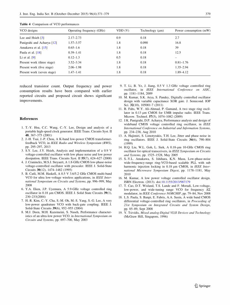
Table 4 Comparison of VCO performances
VCO designs Operating frequency (GHz) VDD (V) Technology (lm) Power consumption (mW)
Lee and Hsieh [3] 2.17–2.73 0.9 0.18 2.7
Panigrahi and Acharya [12] 1.57–3.57 1.8 0.090 16.8
Amakawa et al. [15] 0.65–1.6 1.8 0.18 39
Paula et al. [18] 0.39–1.41 1.8 0.18 12.5
Li et al. [9] 0.12–1.3 0.5 0.18 –
Present work (three stage) 3.52–3.34 1.8 0.18 0.81–1.76
Present work (five stage) 2.06–1.98 1.8 0.18 1.35–2.94
Present work (seven stage) 1.47–1.41 1.8 0.18 1.89–4.12
J. Inst. Eng. India Ser. B (October–Decmber 2015) 96(4):371–379 379
123