Embed Size (px)
Citation preview
Page 1
IS2020/21/23/25 SoC
Bluetooth® 4.1 Stereo Audio SOC
Features
System Specification Compliant with Bluetooth Specification v.4.1
(EDR) in 2.4 GHz ISM band It supports following profiles :
- HFP 1.6 - HSP 1.1 - A2DP 1.2 - AVRCP 1.5 - SPP 1.0 - PBAP 1.0
Baseband Hardware
16MHz main clock input
Built-in internal ROM for program memory
Support to connect to two hosts ( phones, tablets…) with HFP or A2DP profiles simultaneously
Adaptive Frequency Hopping (AFH) avoids occupied RF channels
Fast Connection supported
RF Hardware
Fully Bluetooth 4.1 (EDR) system in 2.4 GHz ISM band.
Combined TX/RX RF terminal simplifies external matching and reduces external antenna switches.
Max. +4dBm output power with 20 dB level control from register control.
Built-in T/R switch for Class 2/3 application
To avoid temperature variation, temperature sensor with temperature calibration is utilized into bias current and gain control.
Fully integrated synthesizer has been created. There requires no external VCO, varactor diode, resonator and loop filter.
Crystal oscillation with built-in digital trimming for temperature/process variations.
Audio processor
Support 64 kb/s A-Law or -Law PCM format, or CVSD (Continuous Variable Slope Delta Modulation) for SCO channel operation.
Noise suppression
Echo suppression
SBC and optional AAC decoding
Packet loss concealment
Build-in four languages (Chinese/ English/ Spanish/ French) voice prompts and 20 events for each one (This function can be set up in “IS20XXS_UI” tool.)
Support SCMS-T
Audio Codec
20 bit DAC and 16 bit ADC codec
98dB SNR DAC playback
Built-in 2 channel 2.3W class-D amplifier for a 4Ω speaker (for IS2025S only)
Peripherals
Built-in Lithium-ion battery charger (up to 350mA)
Integrate 3V, 1.8V configurable switching regulator and LDO
Built-in ADC for battery monitor and voltage sense.
A line-in port for external audio input
Two LED drivers
Flexible HCI interface High speed HCI-UART (Universal
Asynchronous Receiver Transmitter) interface (up to 921600bps)
Package
5x6.5mm2 48QFN package (IS2021S)
7x7mm2 56QFN package (IS2020S, IS2023S)
8x8mm2 68QFN package (IS2025S)
Description
Stereo Audio Chip is a compact, highly
integrated, CMOS single-chip RF and
baseband IC for Bluetooth v4.1 with Enhanced
Data Rate 2.4GHz applications. This chip is
fully compliant with Bluetooth specification and
completely backward-compatible with Bluetooth
3.0, 2.0 or 1.2 systems.
It incorporates Bluetooth 1M/2M/3Mbps RF,
single-cycle 8bit MCU, TX/RX modem, 5-port
memory controller, task/hopping controller,
Stereo Audio SoC
Page 2
UART interface, and MICROCHIP’s own
Bluetooth software stack to achieve the
required BT v4.1 with EDR functions.
To provide the superior audio and voice
quality, it also integrates a DSP co-processor, a
PLL, and a CODEC dedicated for voice and
audio applications.
For voice, not only basic CVSD encoding and
decoding but also enhanced noise reduction
and echo cancellation are implemented by the
built-in DSP to achieve better quality in both
sending and receiving sides. For the enhanced
audio applications, SBC/AAC_LC decoding
functions can be also carried out by DSP to
satisfy Bluetooth A2DP requirements.
In addition, to minimize the external
components required for portable devices, a
battery voltage sensor, battery charger, a
switching regulator and LDO are integrated to
reduce system BOM cost for various Bluetooth
applications.
As the market of portable/wireless speakers
demand is increasing, a stereo 2 channels
2.3W class-D amplifier which provides up to
100dB SNR is also built-in to reduce BOM cost
and PCB area.
Applications
Stereo headsets
Portable speakerphones
Stereo Audio SoC
Page 3
Table of Contents
1.0 DEVICE OVERVIEW ................................................................................................................................... 4 2.0 KEY FEATURES TABLE .............................................................................................................................. 5 3.0 PIN DESCRIPTION AND POWER SUPPLY ............................................................................................... 6 4.0 TRANSCEIVER .......................................................................................................................................... 19 5.0 MICROPROCESSOR ................................................................................................................................ 20 6.0 AUDIO ........................................................................................................................................................ 21 7.0 POWER MANAGEMENT UNIT .................................................................................................................. 23 8.0 GENERAL PURPOSE IOs ......................................................................................................................... 25 9.0 OPERATION WITH EXTERNAL MCU ....................................................................................................... 26 10.0 I2S APPLICATION .................................................................................................................................... 31 11.0 ANTENNA PLACEMENT RULE .............................................................................................................. 33 12.0 SPECIFICATIONS ................................................................................................................................... 34 13.0 REFERENCE CIRCUIT ............................................................................................................................ 41 14.0 PACKAGE INFORMATION ...................................................................................................................... 46 15.0 REFLOW PROFILE AND STORAGE CINDITION ................................................................................... 54
Abbreviations List: HFP: Hands-free Profile AVRCP: Audio Video Remote Control Profile A2DP: Advanced Audio Distribution Profile PBAP: Phone Book Access Profile HSP: Headset Profile SPP: Serial Port Profile NFC: Near Field Communication CDA: Class D Amplifier SCMS-T: Serial Copy Management System
Stereo Audio SoC
Page 4
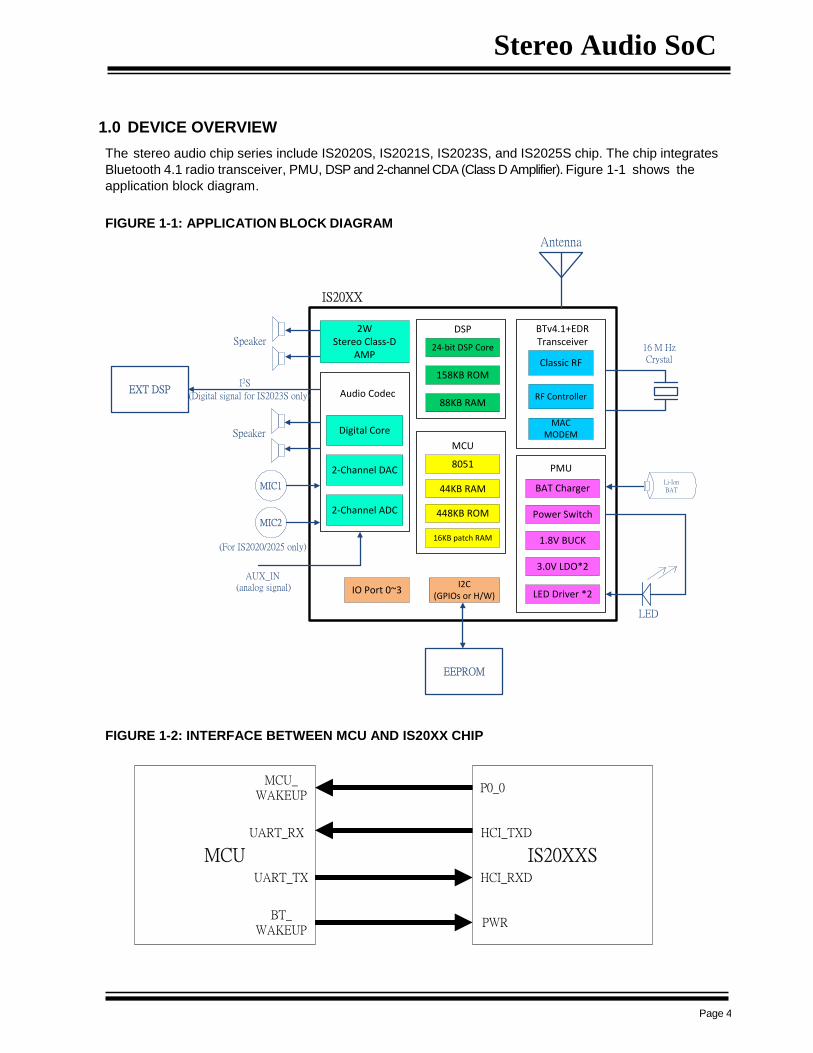
1.0 DEVICE OVERVIEW
The stereo audio chip series include IS2020S, IS2021S, IS2023S, and IS2025S chip. The chip integrates
Bluetooth 4.1 radio transceiver, PMU, DSP and 2-channel CDA (Class D Amplifier). Figure 1-1 shows the
application block diagram.
FIGURE 1-1: APPLICATION BLOCK DIAGRAM
FIGURE 1-2: INTERFACE BETWEEN MCU AND IS20XX CHIP
IS20XXS
HCI_TXD
HCI_RXD
PWR
P0_0
MCUUART_TX
UART_RX
MCU_WAKEUP
BT_WAKEUP
8051
16KB patch RAM
448KB ROM
44KB RAM
24-bit DSP Core
MCU
158KB ROM
88KB RAM
DSP
IS20XX
Classic RF
MACMODEM
BTv4.1+EDRTransceiver
RF Controller
Antenna
16 M Hz Crystal
EEPROM
Power Switch
LED
BAT Charger
1.8V BUCK
3.0V LDO*2
LED Driver *2
PMULi-Ion BAT
(Digital signal for IS2023S only)
2-Channel DAC
Digital Core
2-Channel ADC
Audio Codec
(For IS2020/2025 only)
Speaker2W
Stereo Class-D AMP
MIC1
MIC2
Speaker
EXT DSPI2S
AUX_IN(analog signal) I2C
(GPIOs or H/W)IO Port 0~3
Stereo Audio SoC
Page 5
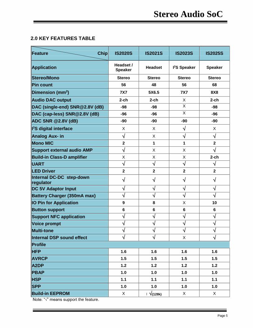
2.0 KEY FEATURES TABLE
Feature Chip IS2020S IS2021S IS2023S IS2025S
Application Headset / Speaker
Headset I2S Speaker Speaker
Stereo/Mono Stereo Stereo Stereo Stereo
Pin count 56 48 56 68
Dimension (mm2) 7X7 5X6.5 7X7 8X8
Audio DAC output 2-ch 2-ch X 2-ch
DAC (single-end) [email protected] (dB) -98 -98 X -98
DAC (cap-less) [email protected] (dB) -96 -96 X -96
ADC SNR @2.8V (dB) -90 -90 -90 -90
I2S digital interface X X X
Analog Aux- in X
Mono MIC 2 1 1 2
Support external audio AMP X X
Build-in Class-D amplifier X X X 2-ch
UART
LED Driver 2 2 2 2
Internal DC-DC step-down regulator
DC 5V Adaptor Input
Battery Charger (350mA max)
IO Pin for Application 9 8 X 10
Button support 6 6 6 6
Support NFC application
Voice prompt
Multi-tone
Internal DSP sound effect X
Profile
HFP 1.6 1.6 1.6 1.6
AVRCP 1.5 1.5 1.5 1.5
A2DP 1.2 1.2 1.2 1.2
PBAP 1.0 1.0 1.0 1.0
HSP 1.1 1.1 1.1 1.1
SPP 1.0 1.0 1.0 1.0
Build-in EEPROM X (128k) X X
Note: “” means support the feature.
Stereo Audio SoC
Page 6
“X” means no support the feature.
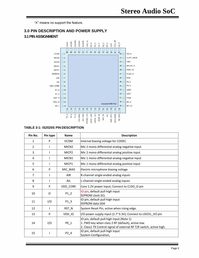
3.0 PIN DESCRIPTION AND POWER SUPPLY
3.1 PIN ASSIGNMENT
TABLE 3-1: IS2020S PIN DESCRIPTION
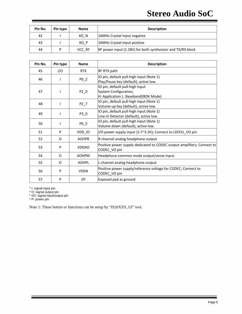
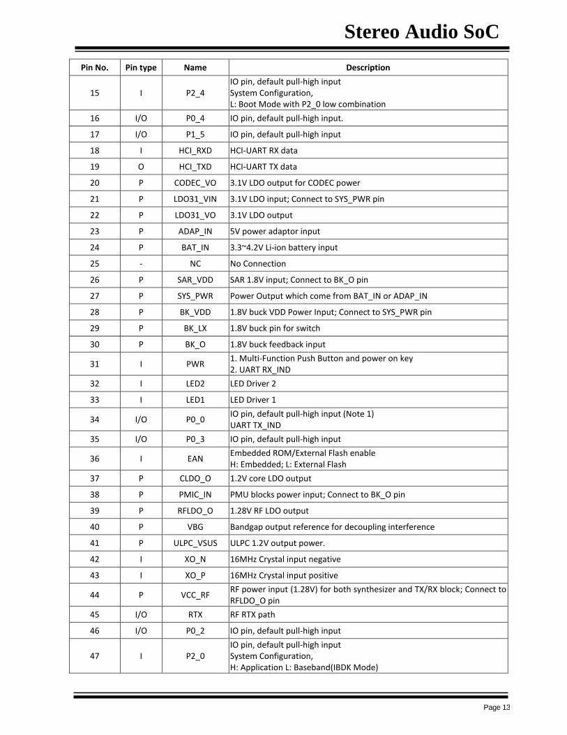
Pin No. Pin type Name Description
1 P VCOM Internal biasing voltage for CODEC
2 I MICN2 Mic 2 mono differential analog negative input
3 I MICP2 Mic 2 mono differential analog positive input
4 I MICN1 Mic 1 mono differential analog negative input
5 I MICP1 Mic 1 mono differential analog positive input
6 P MIC_BIAS Electric microphone biasing voltage
7 I AIR R-channel single-ended analog inputs
8 I AIL L-channel single-ended analog inputs
9 P VDD_CORE Core 1.2V power input; Connect to CLDO_O pin
10 O P1_2 IO pin, default pull-high input EEPROM clock SCL
11 I/O P1_3 IO pin, default pull-high input EEPROM data SDA
12 I RST_N System Reset Pin, active when rising edge.
13 P VDD_IO I/O power supply input (2.7~3.3V); Connect to LDO31_VO pin
14 I/O P0_1 IO pin, default pull-high input (Note 1) 1. FWD key when class 2 RF (default), active low. 2. Class1 TX Control signal of external RF T/R switch, active high.
15 I P2_4 IO pin, default pull-high input System Configuration,
Stereo Audio SoC
Page 7
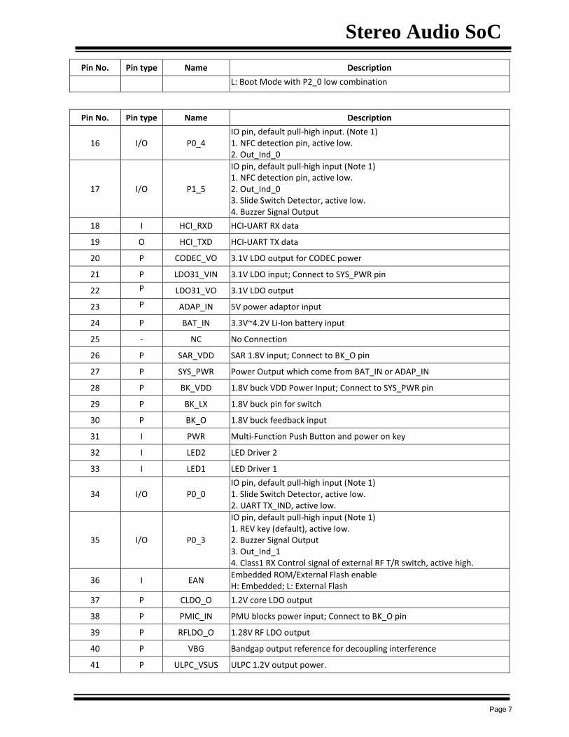
Pin No. Pin type Name Description
L: Boot Mode with P2_0 low combination
Pin No. Pin type Name Description
16 I/O P0_4 IO pin, default pull-high input. (Note 1) 1. NFC detection pin, active low. 2. Out_Ind_0
17 I/O P1_5
IO pin, default pull-high input (Note 1) 1. NFC detection pin, active low. 2. Out_Ind_0 3. Slide Switch Detector, active low. 4. Buzzer Signal Output
18 I HCI_RXD HCI-UART RX data
19 O HCI_TXD HCI-UART TX data
20 P CODEC_VO 3.1V LDO output for CODEC power
21 P LDO31_VIN 3.1V LDO input; Connect to SYS_PWR pin
22 P LDO31_VO 3.1V LDO output
23 P ADAP_IN 5V power adaptor input
24 P BAT_IN 3.3V~4.2V Li-Ion battery input
25 - NC No Connection
26 P SAR_VDD SAR 1.8V input; Connect to BK_O pin
27 P SYS_PWR Power Output which come from BAT_IN or ADAP_IN
28 P BK_VDD 1.8V buck VDD Power Input; Connect to SYS_PWR pin
29 P BK_LX 1.8V buck pin for switch
30 P BK_O 1.8V buck feedback input
31 I PWR Multi-Function Push Button and power on key
32 I LED2 LED Driver 2
33 I LED1 LED Driver 1
34 I/O P0_0 IO pin, default pull-high input (Note 1) 1. Slide Switch Detector, active low. 2. UART TX_IND, active low.
35 I/O P0_3
IO pin, default pull-high input (Note 1) 1. REV key (default), active low. 2. Buzzer Signal Output 3. Out_Ind_1 4. Class1 RX Control signal of external RF T/R switch, active high.
36 I EAN Embedded ROM/External Flash enable H: Embedded; L: External Flash
37 P CLDO_O 1.2V core LDO output
38 P PMIC_IN PMU blocks power input; Connect to BK_O pin
39 P RFLDO_O 1.28V RF LDO output
40 P VBG Bandgap output reference for decoupling interference
41 P ULPC_VSUS ULPC 1.2V output power.
Stereo Audio SoC
Page 8
Pin No. Pin type Name Description
42 I XO_N 16MHz Crystal input negative
43 I XO_P 16MHz Crystal input positive
44 P VCC_RF RF power input (1.28V) for both synthesizer and TX/RX block
Pin No. Pin type Name Description
45 I/O RTX RF RTX path
46 I P0_2 IO pin, default pull-high input (Note 1) Play/Pause key (default), active low.
47 I P2_0 IO pin, default pull-high input System Configuration, H: Application L: Baseband(IBDK Mode)
48 I P2_7 IO pin, default pull-high input (Note 1) Volume up key (default), active low.
49 I P3_0 IO pin, default pull-high input (Note 1) Line-in Detector (default), active low.
50 I P0_5 IO pin, default pull-high input (Note 1) Volume down (default), active low.
51 P VDD_IO I/O power supply input (2.7~3.3V); Connect to LDO31_VO pin
52 O AOHPR R-channel analog headphone output
53 P VDDAO Positive power supply dedicated to CODEC output amplifiers; Connect to CODEC_VO pin
54 O AOHPM Headphone common mode output/sense input.
55 O AOHPL L-channel analog headphone output
56 P VDDA Positive power supply/reference voltage for CODEC; Connect to CODEC_VO pin
57 P EP Exposed pad as ground
* I: signal input pin * O: signal output pin * I/O: signal input/output pin * P: power pin
Note 1: These button or functions can be setup by “IS20XXS_UI” tool.
Stereo Audio SoC
Page 9
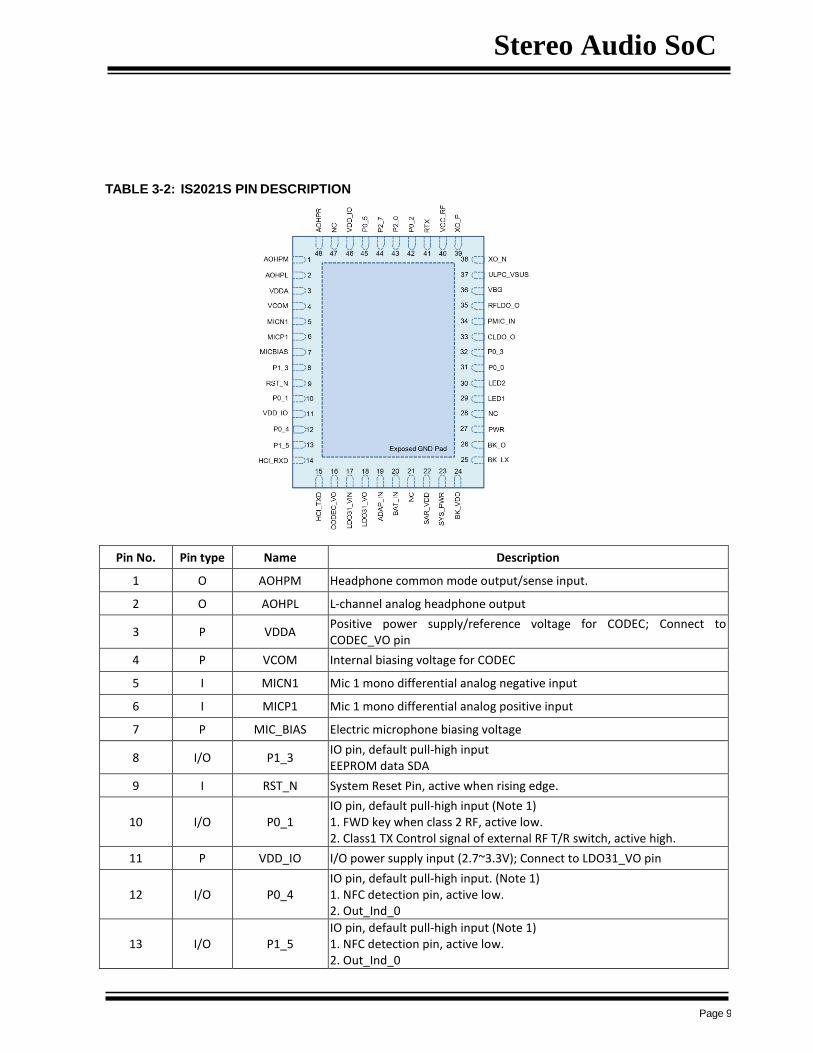
TABLE 3-2: IS2021S PIN DESCRIPTION
Pin No. Pin type Name Description
1 O AOHPM Headphone common mode output/sense input.
2 O AOHPL L-channel analog headphone output
3 P VDDA Positive power supply/reference voltage for CODEC; Connect to CODEC_VO pin
4 P VCOM Internal biasing voltage for CODEC
5 I MICN1 Mic 1 mono differential analog negative input
6 I MICP1 Mic 1 mono differential analog positive input
7 P MIC_BIAS Electric microphone biasing voltage
8 I/O P1_3 IO pin, default pull-high input EEPROM data SDA
9 I RST_N System Reset Pin, active when rising edge.
10 I/O P0_1 IO pin, default pull-high input (Note 1) 1. FWD key when class 2 RF, active low. 2. Class1 TX Control signal of external RF T/R switch, active high.
11 P VDD_IO I/O power supply input (2.7~3.3V); Connect to LDO31_VO pin
12 I/O P0_4 IO pin, default pull-high input. (Note 1) 1. NFC detection pin, active low. 2. Out_Ind_0
13 I/O P1_5 IO pin, default pull-high input (Note 1) 1. NFC detection pin, active low. 2. Out_Ind_0
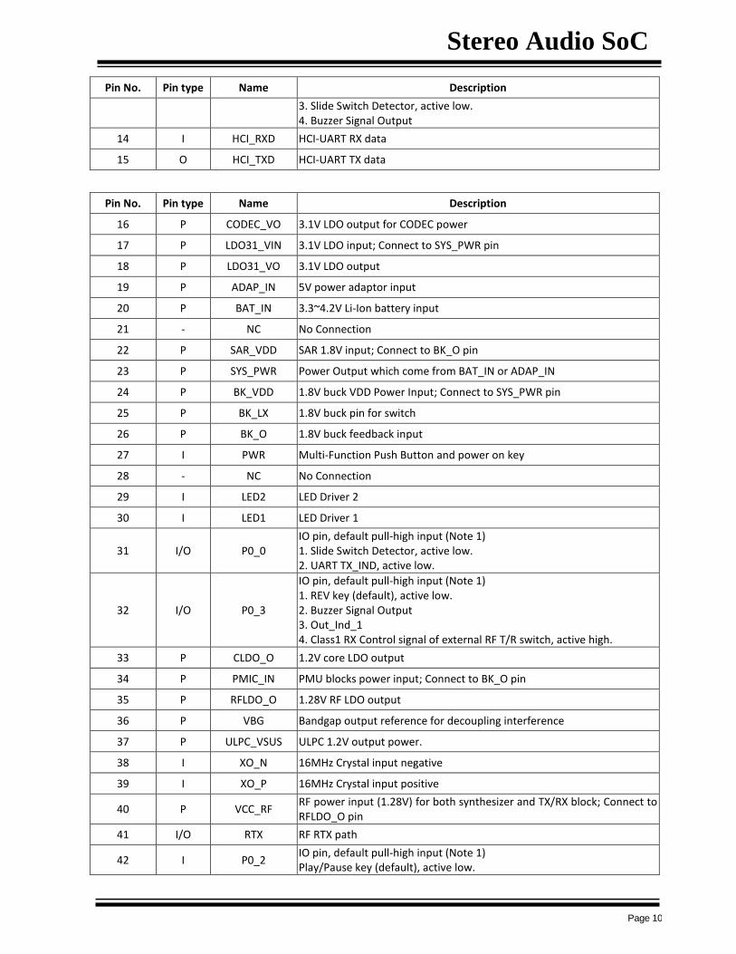
Stereo Audio SoC
Page 10
Pin No. Pin type Name Description
3. Slide Switch Detector, active low. 4. Buzzer Signal Output
14 I HCI_RXD HCI-UART RX data
15 O HCI_TXD HCI-UART TX data
Pin No. Pin type Name Description
16 P CODEC_VO 3.1V LDO output for CODEC power
17 P LDO31_VIN 3.1V LDO input; Connect to SYS_PWR pin
18 P LDO31_VO 3.1V LDO output
19 P ADAP_IN 5V power adaptor input
20 P BAT_IN 3.3~4.2V Li-Ion battery input
21 - NC No Connection
22 P SAR_VDD SAR 1.8V input; Connect to BK_O pin
23 P SYS_PWR Power Output which come from BAT_IN or ADAP_IN
24 P BK_VDD 1.8V buck VDD Power Input; Connect to SYS_PWR pin
25 P BK_LX 1.8V buck pin for switch
26 P BK_O 1.8V buck feedback input
27 I PWR Multi-Function Push Button and power on key
28 - NC No Connection
29 I LED2 LED Driver 2
30 I LED1 LED Driver 1
31 I/O P0_0 IO pin, default pull-high input (Note 1) 1. Slide Switch Detector, active low. 2. UART TX_IND, active low.
32 I/O P0_3
IO pin, default pull-high input (Note 1) 1. REV key (default), active low. 2. Buzzer Signal Output 3. Out_Ind_1 4. Class1 RX Control signal of external RF T/R switch, active high.
33 P CLDO_O 1.2V core LDO output
34 P PMIC_IN PMU blocks power input; Connect to BK_O pin
35 P RFLDO_O 1.28V RF LDO output
36 P VBG Bandgap output reference for decoupling interference
37 P ULPC_VSUS ULPC 1.2V output power.
38 I XO_N 16MHz Crystal input negative
39 I XO_P 16MHz Crystal input positive
40 P VCC_RF RF power input (1.28V) for both synthesizer and TX/RX block; Connect to RFLDO_O pin
41 I/O RTX RF RTX path
42 I P0_2 IO pin, default pull-high input (Note 1) Play/Pause key (default), active low.

Stereo Audio SoC
Page 11
Pin No. Pin type Name Description
43 I P2_0 IO pin, default pull-high input (Note 1) System Configuration, H: Application L: Baseband(IBDK Mode)
44 I P2_7 IO pin, default pull-high input (Note 1) Volume up key (default), active low.
45 I P0_5 IO pin, default pull-high input (Note 1) Volume down (default), active low.
Pin No. Pin type Name Description
46 P VDD_IO I/O power supply input (2.7~3.3V); Connect to LDO31_VO pin
47 - NC No Connection.
48 O AOHPR R-channel analog headphone output
49 P EP Exposed pad as ground
* I: signal input pin * O: signal output pin * I/O: signal input/output pin * P: power pin
Note 1: These button or functions can be setup by “IS20XXS_UI” tool.
Stereo Audio SoC
Page 12
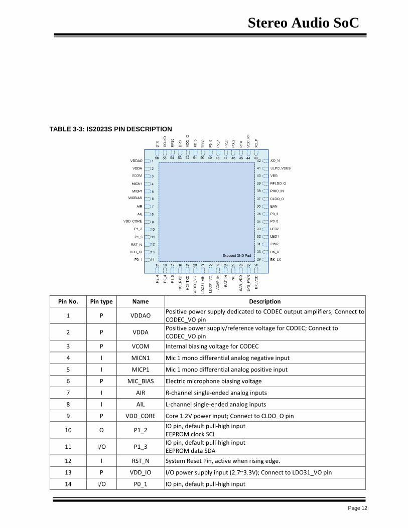
TABLE 3-3: IS2023S PIN DESCRIPTION
Pin No. Pin type Name Description
1 P VDDAO Positive power supply dedicated to CODEC output amplifiers; Connect to CODEC_VO pin
2 P VDDA Positive power supply/reference voltage for CODEC; Connect to CODEC_VO pin
3 P VCOM Internal biasing voltage for CODEC
4 I MICN1 Mic 1 mono differential analog negative input
5 I MICP1 Mic 1 mono differential analog positive input
6 P MIC_BIAS Electric microphone biasing voltage
7 I AIR R-channel single-ended analog inputs
8 I AIL L-channel single-ended analog inputs
9 P VDD_CORE Core 1.2V power input; Connect to CLDO_O pin
10 O P1_2 IO pin, default pull-high input EEPROM clock SCL
11 I/O P1_3 IO pin, default pull-high input EEPROM data SDA
12 I RST_N System Reset Pin, active when rising edge.
13 P VDD_IO I/O power supply input (2.7~3.3V); Connect to LDO31_VO pin
14 I/O P0_1 IO pin, default pull-high input
Stereo Audio SoC
Page 13
Pin No. Pin type Name Description
15 I P2_4 IO pin, default pull-high input System Configuration, L: Boot Mode with P2_0 low combination
16 I/O P0_4 IO pin, default pull-high input.
17 I/O P1_5 IO pin, default pull-high input
18 I HCI_RXD HCI-UART RX data
19 O HCI_TXD HCI-UART TX data
20 P CODEC_VO 3.1V LDO output for CODEC power
21 P LDO31_VIN 3.1V LDO input; Connect to SYS_PWR pin
22 P LDO31_VO 3.1V LDO output
23 P ADAP_IN 5V power adaptor input
24 P BAT_IN 3.3~4.2V Li-ion battery input
25 - NC No Connection
26 P SAR_VDD SAR 1.8V input; Connect to BK_O pin
27 P SYS_PWR Power Output which come from BAT_IN or ADAP_IN
28 P BK_VDD 1.8V buck VDD Power Input; Connect to SYS_PWR pin
29 P BK_LX 1.8V buck pin for switch
30 P BK_O 1.8V buck feedback input
31 I PWR 1. Multi-Function Push Button and power on key 2. UART RX_IND
32 I LED2 LED Driver 2
33 I LED1 LED Driver 1
34 I/O P0_0 IO pin, default pull-high input (Note 1) UART TX_IND
35 I/O P0_3 IO pin, default pull-high input
36 I EAN Embedded ROM/External Flash enable H: Embedded; L: External Flash
37 P CLDO_O 1.2V core LDO output
38 P PMIC_IN PMU blocks power input; Connect to BK_O pin
39 P RFLDO_O 1.28V RF LDO output
40 P VBG Bandgap output reference for decoupling interference
41 P ULPC_VSUS ULPC 1.2V output power.
42 I XO_N 16MHz Crystal input negative
43 I XO_P 16MHz Crystal input positive
44 P VCC_RF RF power input (1.28V) for both synthesizer and TX/RX block; Connect to RFLDO_O pin
45 I/O RTX RF RTX path
46 I/O P0_2 IO pin, default pull-high input
47 I P2_0 IO pin, default pull-high input System Configuration, H: Application L: Baseband(IBDK Mode)
Stereo Audio SoC
Page 14
Pin No. Pin type Name Description
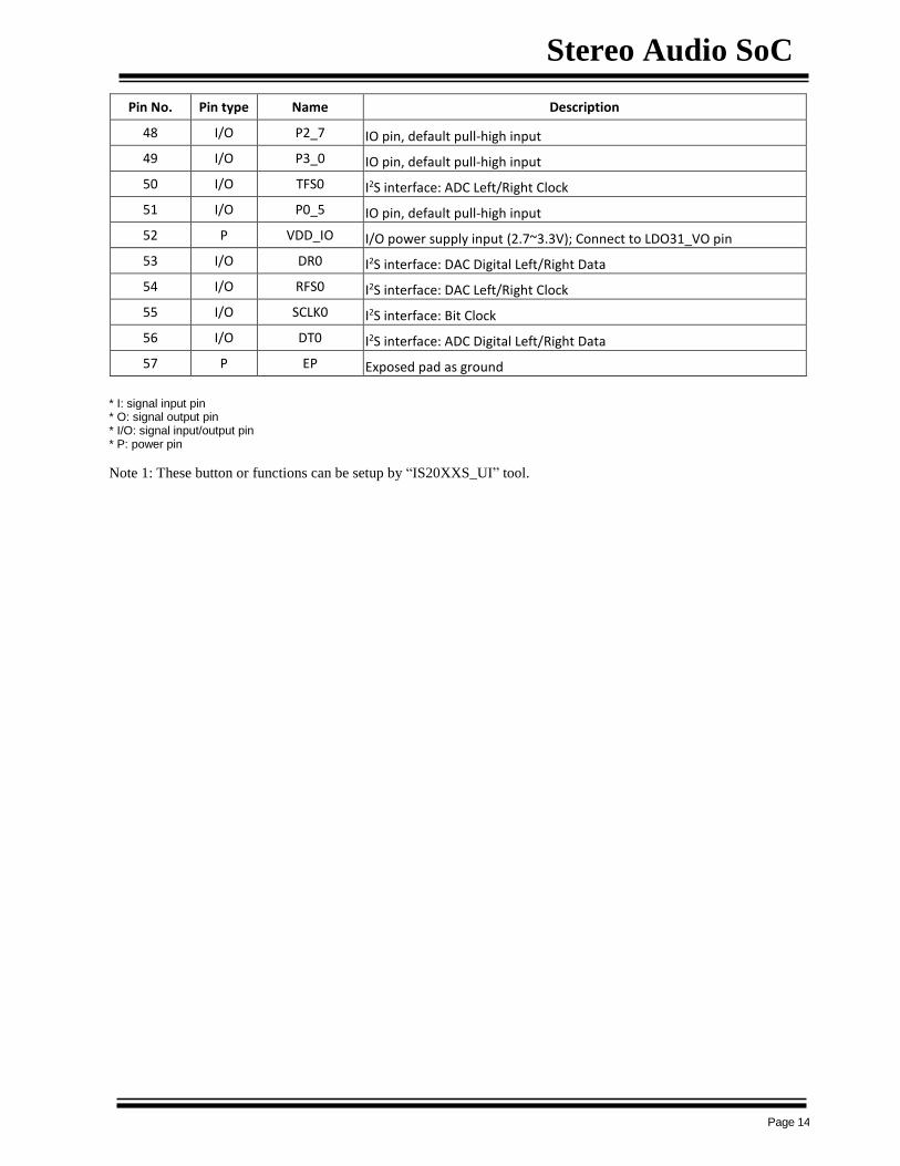
48 I/O P2_7 IO pin, default pull-high input
49 I/O P3_0 IO pin, default pull-high input
50 I/O TFS0 I2S interface: ADC Left/Right Clock
51 I/O P0_5 IO pin, default pull-high input
52 P VDD_IO I/O power supply input (2.7~3.3V); Connect to LDO31_VO pin
53 I/O DR0 I2S interface: DAC Digital Left/Right Data
54 I/O RFS0 I2S interface: DAC Left/Right Clock
55 I/O SCLK0 I2S interface: Bit Clock
56 I/O DT0 I2S interface: ADC Digital Left/Right Data
57 P EP Exposed pad as ground
* I: signal input pin * O: signal output pin * I/O: signal input/output pin * P: power pin
Note 1: These button or functions can be setup by “IS20XXS_UI” tool.
Stereo Audio SoC
Page 15
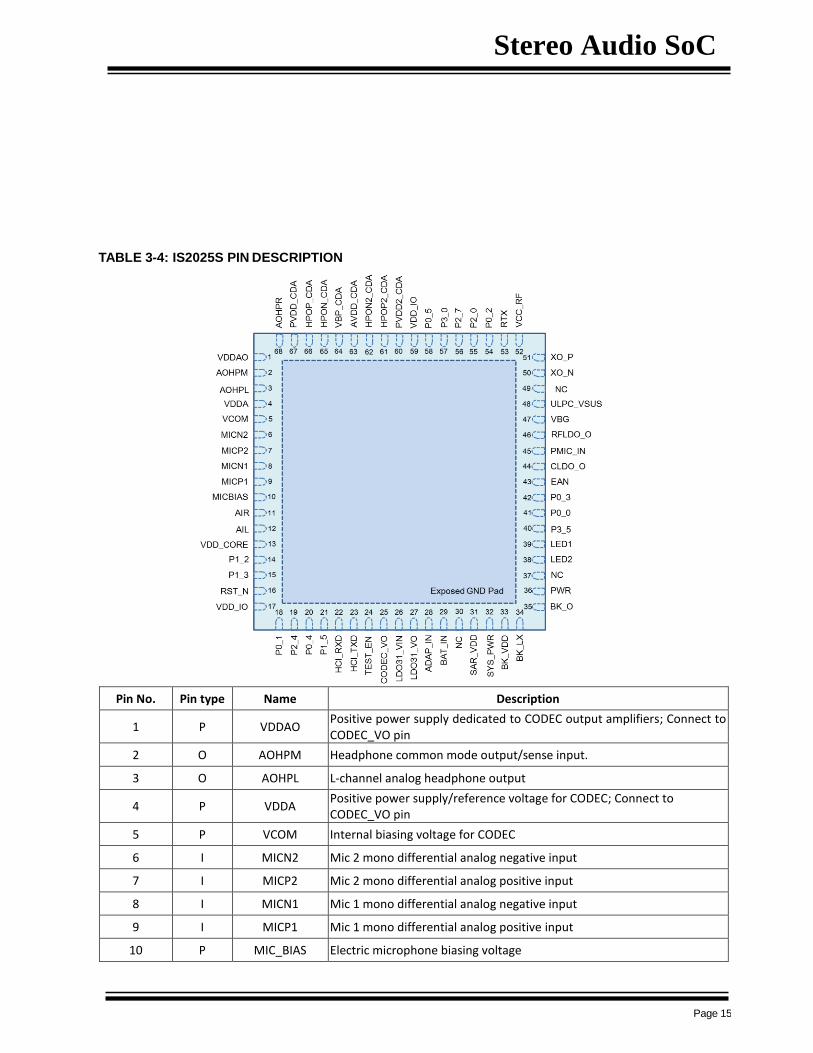
TABLE 3-4: IS2025S PIN DESCRIPTION
Pin No. Pin type Name Description
1 P VDDAO Positive power supply dedicated to CODEC output amplifiers; Connect to CODEC_VO pin
2 O AOHPM Headphone common mode output/sense input.
3 O AOHPL L-channel analog headphone output
4 P VDDA Positive power supply/reference voltage for CODEC; Connect to CODEC_VO pin
5 P VCOM Internal biasing voltage for CODEC
6 I MICN2 Mic 2 mono differential analog negative input
7 I MICP2 Mic 2 mono differential analog positive input
8 I MICN1 Mic 1 mono differential analog negative input
9 I MICP1 Mic 1 mono differential analog positive input
10 P MIC_BIAS Electric microphone biasing voltage
Stereo Audio SoC
Page 16
Pin No. Pin type Name Description
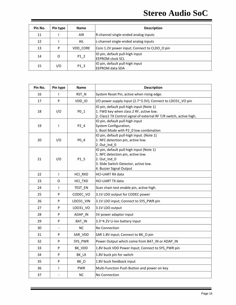
11 I AIR R-channel single-ended analog inputs
12 I AIL L-channel single-ended analog inputs
13 P VDD_CORE Core 1.2V power input; Connect to CLDO_O pin
14 O P1_2 IO pin, default pull-high input EEPROM clock SCL
15 I/O P1_3 IO pin, default pull-high input EEPROM data SDA
Pin No. Pin type Name Description
16 I RST_N System Reset Pin, active when rising edge.
17 P VDD_IO I/O power supply input (2.7~3.3V); Connect to LDO31_VO pin
18 I/O P0_1 IO pin, default pull-high input (Note 1) 1. FWD key when class 2 RF, active low. 2. Class1 TX Control signal of external RF T/R switch, active high.
19 I P2_4 IO pin, default pull-high input System Configuration, L: Boot Mode with P2_0 low combination
20 I/O P0_4 IO pin, default pull-high input. (Note 1) 1. NFC detection pin, active low. 2. Out_Ind_0
21 I/O P1_5
IO pin, default pull-high input (Note 1) 1. NFC detection pin, active low. 2. Out_Ind_0 3. Slide Switch Detector, active low. 4. Buzzer Signal Output
22 I HCI_RXD HCI-UART RX data
23 O HCI_TXD HCI-UART TX data
24 I TEST_EN Scan chain test enable pin, active high.
25 P CODEC_VO 3.1V LDO output for CODEC power
26 P LDO31_VIN 3.1V LDO input; Connect to SYS_PWR pin
27 P LDO31_VO 3.1V LDO output
28 P ADAP_IN 5V power adaptor input
29 P BAT_IN 3.3~4.2V Li-Ion battery input
30 - NC No Connection
31 P SAR_VDD SAR 1.8V input; Connect to BK_O pin
32 P SYS_PWR Power Output which come from BAT_IN or ADAP_IN
33 P BK_VDD 1.8V buck VDD Power Input; Connect to SYS_PWR pin
34 P BK_LX 1.8V buck pin for switch
35 P BK_O 1.8V buck feedback input
36 I PWR Multi-Function Push Button and power on key
37 - NC No Connection
Stereo Audio SoC
Page 17
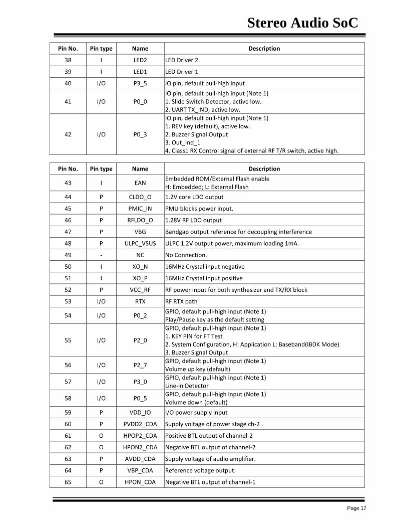
Pin No. Pin type Name Description
38 I LED2 LED Driver 2
39 I LED1 LED Driver 1
40 I/O P3_5 IO pin, default pull-high input
41 I/O P0_0 IO pin, default pull-high input (Note 1) 1. Slide Switch Detector, active low. 2. UART TX_IND, active low.
42 I/O P0_3
IO pin, default pull-high input (Note 1) 1. REV key (default), active low. 2. Buzzer Signal Output 3. Out_Ind_1 4. Class1 RX Control signal of external RF T/R switch, active high.
Pin No. Pin type Name Description
43 I EAN Embedded ROM/External Flash enable H: Embedded; L: External Flash
44 P CLDO_O 1.2V core LDO output
45 P PMIC_IN PMU blocks power input.
46 P RFLDO_O 1.28V RF LDO output
47 P VBG Bandgap output reference for decoupling interference
48 P ULPC_VSUS ULPC 1.2V output power, maximum loading 1mA.
49 - NC No Connection.
50 I XO_N 16MHz Crystal input negative
51 I XO_P 16MHz Crystal input positive
52 P VCC_RF RF power input for both synthesizer and TX/RX block
53 I/O RTX RF RTX path
54 I/O P0_2 GPIO, default pull-high input (Note 1) Play/Pause key as the default setting
55 I/O P2_0
GPIO, default pull-high input (Note 1) 1. KEY PIN for FT Test 2. System Configuration, H: Application L: Baseband(IBDK Mode) 3. Buzzer Signal Output
56 I/O P2_7 GPIO, default pull-high input (Note 1) Volume up key (default)
57 I/O P3_0 GPIO, default pull-high input (Note 1) Line-in Detector
58 I/O P0_5 GPIO, default pull-high input (Note 1) Volume down (default)
59 P VDD_IO I/O power supply input
60 P PVDD2_CDA Supply voltage of power stage ch-2 .
61 O HPOP2_CDA Positive BTL output of channel-2
62 O HPON2_CDA Negative BTL output of channel-2
63 P AVDD_CDA Supply voltage of audio amplifier.
64 P VBP_CDA Reference voltage output.
65 O HPON_CDA Negative BTL output of channel-1
Stereo Audio SoC
Page 18
Pin No. Pin type Name Description
66 O HPOP_CDA Positive BTL output of channel-1
67 P PVDD_CDA Supply voltage of power stage ch-1
68 O AOHPR R-channel analog headphone output
69 P EP Exposed pad as ground
* I: signal input pin * O: signal output pin * I/O: signal input/output pin * P: power pin
Note 1: These button or functions can be setup by “IS20XXS_UI” tool.
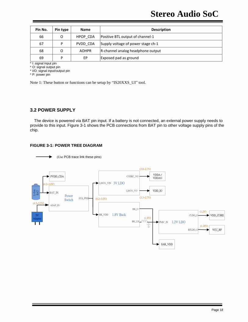
3.2 POWER SUPPLY
The device is powered via BAT pin input. If a battery is not connected, an external power supply needs to provide to this input. Figure 3-1 shows the PCB connections from BAT pin to other voltage supply pins of the chip.
FIGURE 3-1: POWER TREE DIAGRAM
(Use PCB trace link these pins)
VDDA /VDDAO
VDD_IO
3V LDO
1.8V Buck
SAR_VDD
LDO31_VIN
CODEC_VO
LDO31_VO
BK_VDD
BK_LX
BK_O
VDD_CORE
VCC_RF
1.2V LDOPMIC_IN
CLDO_O
RFLDO_O
PVDD_CDA
Li-
Ion
BA
T
BAT_IN
ADAP_IN
SYS_PWRPower Switch
5V Adapter
(4.2~3.0V)
(4.5~5.5V)
(4.2~3.0V)
(3.0~2.7V)
(3.3~2.7V)
(1.8V)
(1.2V)
(1.28V)
Stereo Audio SoC
Page 19
4.0 TRANSCEIVER
The stereo audio chip is designed and optimized for Bluetooth 2.4 GHz system. It contains a complete radio frequency transmitter/receiver section. An internal synthesizer generates a stable clock for synchronize with another device.
4.1 TRANSMITTER
The internal PA has a maximum output power of +4dBm with 20dB power level control. This is applied into Class2/3 radios without external RF PA.
The transmitter directly performs IQ conversion to minimize the frequency drift, and it can excess 20dB power range with temperature compensation mechanism.
4.2 RECEVIER
The LNA operates with TR-combined mode for single port application. It can save a pin on package and without an external TX/RX switch.
The ADC is utilized to sample the input analog wave and convert into digital signal for de-modulator analysis. A channel filter has been integrated into receiver channel before the ADC, which to reduce the external component count and increase the anti-interference capability.
The image rejection filter is used to reject image frequency for low-IF architecture. This filter for low-IF architecture is intent to reduce external BPF component for super heterodyne architecture.
RSSI signal is feedback to the processor to control the RF output power to make a good tradeoff for effective distance and current consumption.
4.3 SYNTHESIZER
A synthesizer generates a clock for radio transceiver operation. There is a VCO inside with tunable internal LC tank. It can reduce variation for components. A crystal oscillation with internal digital trimming circuit provides a stable clock for synthesizer.
4.4 MODEM
For Bluetooth v1.2 specification and below, 1 Mbps was the standard data rate based on Gaussian Frequency Shift Keying (GFSK) modulation scheme. This basic rate modem meets BDR requirements of Bluetooth v2.0 with EDR specification.
For Bluetooth v2.0 with EDR specification, Enhanced Data Rate (EDR) has been introduced to provide 2 and 3 Mbps data rates as well as 1 Mbps. This enhanced data rate modem meets EDR requirements of Bluetooth v2.0 with EDR specification. For the viewpoint of baseband, both BDR and EDR utilize the same 1MHz symbol rate and 1.6 KHz slot rate. For BDR, 1 symbol represents 1 bit. However each symbol in the payload part of EDR packets represents 2 or 3 bits. This is achieved by using two different modulations, π/4 DQPSK and 8DPSK.
4.5 AFH (Adaptive Frequency Hopping)
Stereo audio chip have AFH function to avoid RF interference. It has an algorithm to check the interference nearby and choice clear channel to transceiver Bluetooth signal.
Stereo Audio SoC
Page 20
5.0 MICROPROCESSOR
A single-cycle 8-bit MCU is built into the stereo audio chip to execute the Bluetooth protocols. It operates from 16MHz to higher frequency where the firmware can dynamically adjust the tradeoff between the computing power and the power consumption. The MCU firmware is hard-wired in ROM to minimize the firmware execution power consumption and to save the external flash cost.
5.1 MEMORY
A synchronous single port RAM interface is used. There are sufficient ROM and RAM to fulfill the requirement of processor. A register bank, a dedicated single port memory and a flash memory are connected to the processor bus. The processor coordinates all the link control procedures and data movement using a set of pointers registers.
5.2 EXTERNAL RESET
The chip provides a watchdog timer to reset the chip. It has an integrated Power-On Reset (POR) circuit that resets all circuits to a known power-on state. This action can also be driven by an external reset signal that can be used to externally control the device, forcing it into a power-on reset state. The RST signal input is active low and no connection is required in most applications.
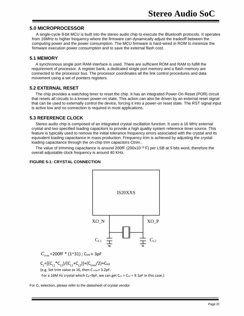
5.3 REFERENCE CLOCK
Stereo audio chip is composed of an integrated crystal oscillation function. It uses a 16 MHz external crystal and two specified loading capacitors to provide a high quality system reference timer source. This feature is typically used to remove the initial tolerance frequency errors associated with the crystal and its equivalent loading capacitance in mass production. Frequency trim is achieved by adjusting the crystal loading capacitance through the on-chip trim capacitors Ctrim..
The value of trimming capacitance is around 200fF (200x10-15 F) per LSB at 5 bits word, therefore the overall adjustable clock frequency is around 40 KHz.
FIGURE 5-1: CRYSTAL CONNECTION
IS20XXS
XO_N XO_P
CL1 CL2
trimC =200fF * (1~31) ; Cint 3pF
CL=[(CL1*CL2)/(CL1+CL2)]+(Ctrim/2)+Cint
(e.g. Set trim value as 16, then C trim= 3.2pF.
For a 16M Hz crystal which CL=9pF, we can get CL1 = CL2 = 9.1pF in this case.)
For CL selection, please refer to the datasheet of crystal vendor
Stereo Audio SoC
Page 21
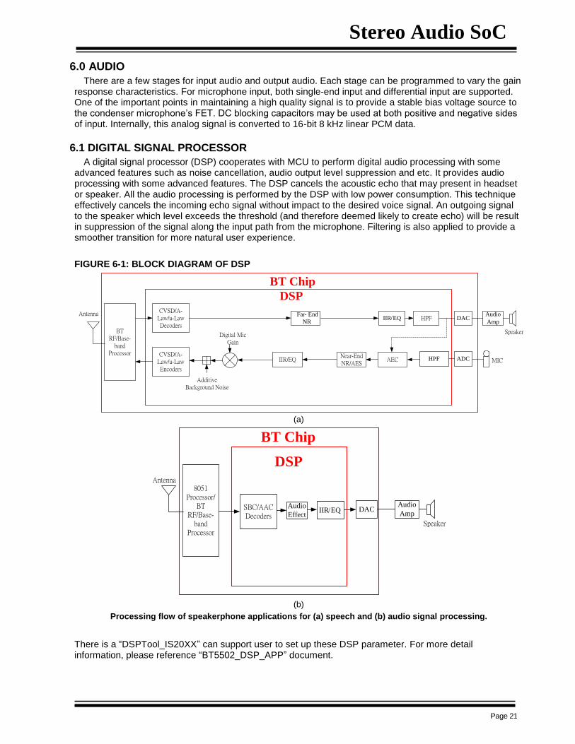
6.0 AUDIO
There are a few stages for input audio and output audio. Each stage can be programmed to vary the gain response characteristics. For microphone input, both single-end input and differential input are supported. One of the important points in maintaining a high quality signal is to provide a stable bias voltage source to the condenser microphone’s FET. DC blocking capacitors may be used at both positive and negative sides of input. Internally, this analog signal is converted to 16-bit 8 kHz linear PCM data.
6.1 DIGITAL SIGNAL PROCESSOR
A digital signal processor (DSP) cooperates with MCU to perform digital audio processing with some advanced features such as noise cancellation, audio output level suppression and etc. It provides audio processing with some advanced features. The DSP cancels the acoustic echo that may present in headset or speaker. All the audio processing is performed by the DSP with low power consumption. This technique effectively cancels the incoming echo signal without impact to the desired voice signal. An outgoing signal to the speaker which level exceeds the threshold (and therefore deemed likely to create echo) will be result in suppression of the signal along the input path from the microphone. Filtering is also applied to provide a smoother transition for more natural user experience.
FIGURE 6-1: BLOCK DIAGRAM OF DSP
Far- End
NRIIR/EQ DAC
Audio
Amp
ADCHPFAECNear-End NR/AES
HPF
Digital Mic Gain
Additive Background Noise
IIR/EQ
CVSD/A-Law/u-Law Decoders
CVSD/A-Law/u-Law Encoders
DSP
BT Chip
BT RF/Base-
band Processor
Speaker
MIC
Antenna
(a)
IIR/EQ DACAudio
AmpSBC/AAC Decoders
DSP
BT Chip
8051 Processor/
BT RF/Base-
band Processor
Audio
Effect
Speaker
Antenna
(b)
Processing flow of speakerphone applications for (a) speech and (b) audio signal processing.
There is a “DSPTool_IS20XX” can support user to set up these DSP parameter. For more detail information, please reference “BT5502_DSP_APP” document.
Stereo Audio SoC
Page 22
6.2 CLASS-D AUDIO AMPLIFIER
The class D amplifier has significant advantage in many applications because of its lower power dissipation which produces less heat. IS2025S chip has built-in a class D amplifier that reduces circuit board space and system cost. The efficiency of the amplifier extends the battery life in portable systems.
The class D amplifier is implemented by using a full-bridge output stage. A full bridge uses two half-bridge stages to drive the load differentially. It provides a good signal to noise ratio (SNR) and enough drive capability for a 4 Ohm speaker driver.
6.3 CODEC
The built-in codec has a high Signal to Noise ratio performance. This built-in codec consist of an analog to digital converter (ADC), a digital to analog converter (DAC) and additional analog circuitry.
6.4 LINE IN (Aux In)
The chip supports one analog line in from external audio source. The analog line in signal can be processed by the DSP to generate different sound effect (Multi-band Dynamic Range Compression, Audio Widening). The sound effect can be set up by DSP tool.
Stereo Audio SoC
Page 23
7.0 POWER MANAGEMENT UNIT
The on-chip Power management Unit (PMU) has two main feature; Lithium Ion battery charging and voltage regulation. A power switch is used to switch over the power source between battery and adaptor automatically. The PMU also provides driving current for 2 LEDs.
7.1 CHARGING A BATTERY
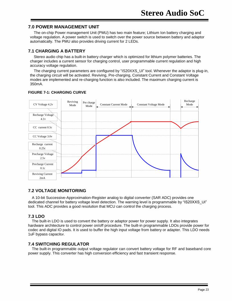
Stereo audio chip has a built-in battery charger which is optimized for lithium polymer batteries. The charger includes a current sensor for charging control, user programmable current regulation and high accuracy voltage regulation.
The charging current parameters are configured by “IS20XXS_UI” tool. Whenever the adaptor is plug-in, the charging circuit will be activated. Reviving, Pre-charging, Constant Current and Constant Voltage modes are implemented and re-charging function is also included. The maximum charging current is 350mA.
FIGURE 7-1: CHARGING CURVE
7.2 VOLTAGE MONITORING
A 10-bit Successive-Approximation-Register analog to digital converter (SAR ADC) provides one dedicated channel for battery voltage level detection. The warning level is programmable by “IS20XXS_UI” tool. This ADC provides a good resolution that MCU can control the charging process.
7.3 LDO
The built-in LDO is used to convert the battery or adaptor power for power supply. It also integrates hardware architecture to control power on/off procedure. The built-in programmable LDOs provide power for codec and digital IO pads. It is used to buffer the high input voltage from battery or adapter. This LDO needs 1uF bypass capacitor.
7.4 SWITCHING REGULATOR
The built-in programmable output voltage regulator can convert battery voltage for RF and baseband core power supply. This converter has high conversion efficiency and fast transient response.
Precharge Voltage
2.5v
CC Voltage 3.0v
CC current 0.5c
Recharge Voltage
4.1v
CV Voltage 4.2v Constant Current Mode Constant Voltage Mode
Recharge
ModePre charge
Mode
Reviving
Mode
Reviving Current
2mA
Precharge Current
0.1c
Recharge current
0.25c
Stereo Audio SoC
Page 24
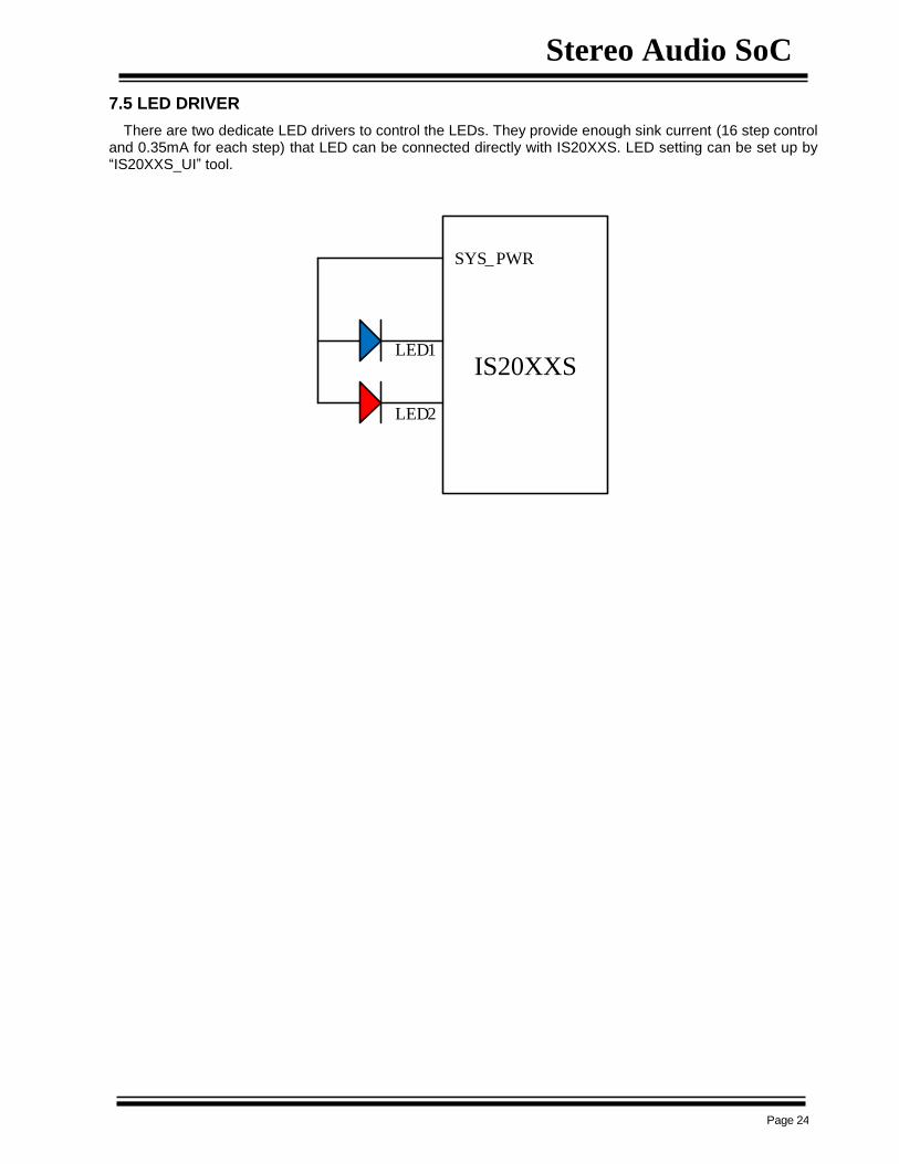
7.5 LED DRIVER
There are two dedicate LED drivers to control the LEDs. They provide enough sink current (16 step control and 0.35mA for each step) that LED can be connected directly with IS20XXS. LED setting can be set up by “IS20XXS_UI” tool.
IS20XXSLED1
LED2
SYS_PWR
Stereo Audio SoC
Page 25
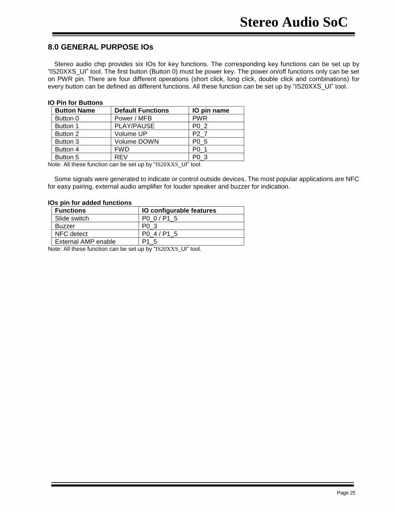
8.0 GENERAL PURPOSE IOs
Stereo audio chip provides six IOs for key functions. The corresponding key functions can be set up by “IS20XXS_UI” tool. The first button (Button 0) must be power key. The power on/off functions only can be set on PWR pin. There are four different operations (short click, long click, double click and combinations) for every button can be defined as different functions. All these function can be set up by “IS20XXS_UI” tool.
IO Pin for Buttons
Button Name Default Functions IO pin name
Button 0 Power / MFB PWR
Button 1 PLAY/PAUSE P0_2
Button 2 Volume UP P2_7
Button 3 Volume DOWN P0_5
Button 4 FWD P0_1
Button 5 REV P0_3 Note: All these function can be set up by “IS20XXS_UI” tool.
Some signals were generated to indicate or control outside devices. The most popular applications are NFC
for easy pairing, external audio amplifier for louder speaker and buzzer for indication.
IOs pin for added functions
Functions IO configurable features
Slide switch P0_0 / P1_5
Buzzer P0_3
NFC detect P0_4 / P1_5
External AMP enable P1_5 Note: All these function can be set up by “IS20XXS_UI” tool.

Stereo Audio SoC
Page 26
9.0 OPERATION WITH EXTERNAL MCU
IS20XXS support UART command set to make an external MCU to control IS20XXS chip. Here is the connection interface between IS20XXS and MCU. FIGURE 9-1: INTERFACE BETWEEN MCU AND IS20XX CHIP
MCU can control IS20XXS chip by UART interface and wakeup IS20XXS by PWR pin. IS20XXS provide
wakeup MCU function by connect to P0_0 pin of IS20XX.
“UART_CommandSet_v154” document provide all UART command which IS20XX support and “IS20XXS_UI” tool will help you to set up your system support UART command.
For more detail description, please reference “UART_CommandSet_v154” document and “IS20XXS_UI” tool.
IS20XXS
HCI_TXD
HCI_RXD
PWR
P0_0
MCUUART_TX
UART_RX
MCU_WAKEUP
BT_WAKEUP
UART interface
UART interface
Stereo Audio SoC
Page 27
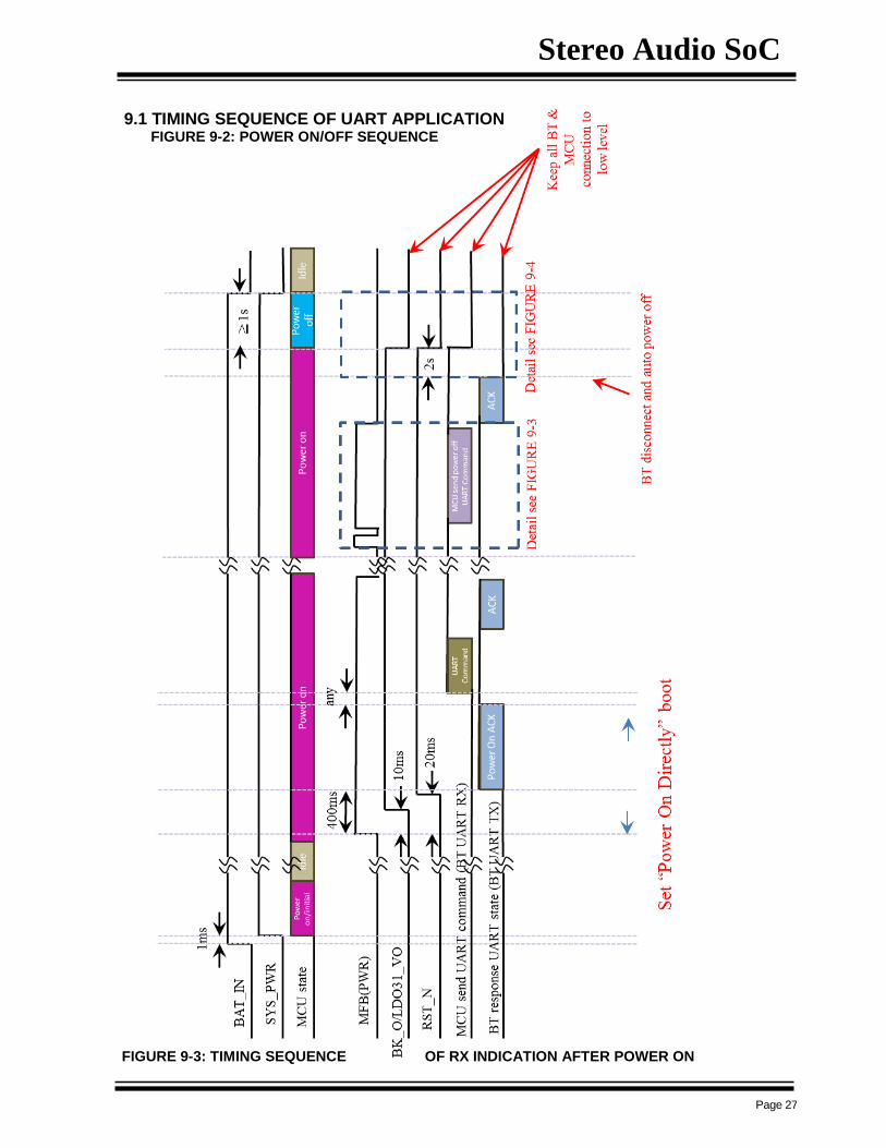
9.1 TIMING SEQUENCE OF UART APPLICATION FIGURE 9-2: POWER ON/OFF SEQUENCE
FIGURE 9-3: TIMING SEQUENCE OF RX INDICATION AFTER POWER ON
Stereo Audio SoC
Page 28
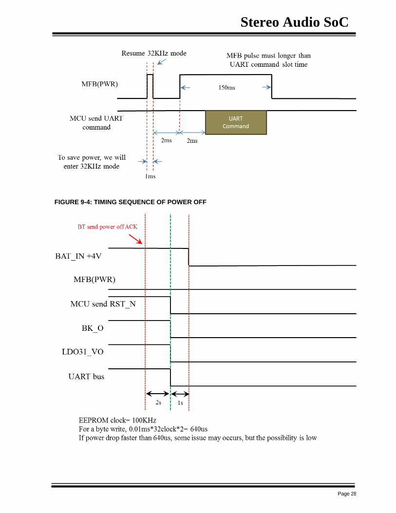
FIGURE 9-4: TIMING SEQUENCE OF POWER OFF
Stereo Audio SoC
Page 29
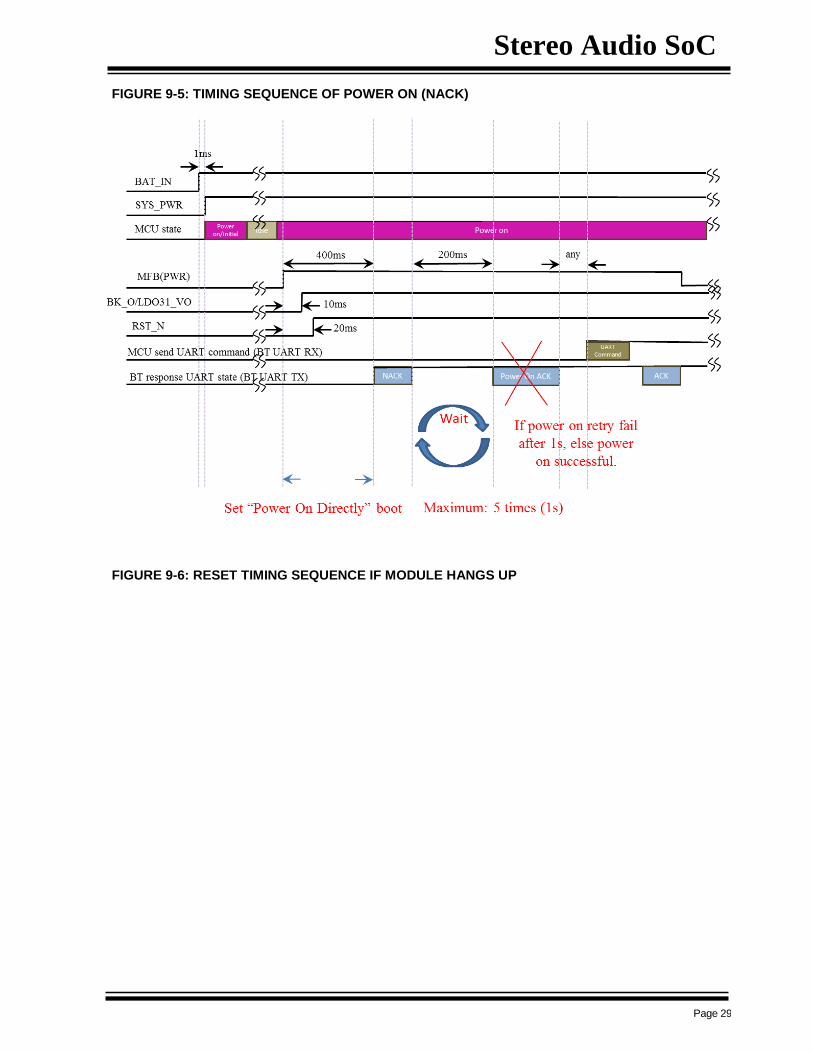
FIGURE 9-5: TIMING SEQUENCE OF POWER ON (NACK)
FIGURE 9-6: RESET TIMING SEQUENCE IF MODULE HANGS UP

Stereo Audio SoC
Page 30
FIGURE 9-7: TIMING SEQUENCE OF POWER DROP PROTECTION
BAT_IN +4V
RST_N from Reset IC
If BT’s BAT use adaptor translates voltage by LDO, we recommend use “Reset IC” to avoid power
off suddenly. Rest IC spec output pin must be “Open Drain”、delay time ≦ 10ms
Recommend part: TCM809SVNB713 or G691L263T73
Power
2.9V ~
Stereo Audio SoC
Page 31
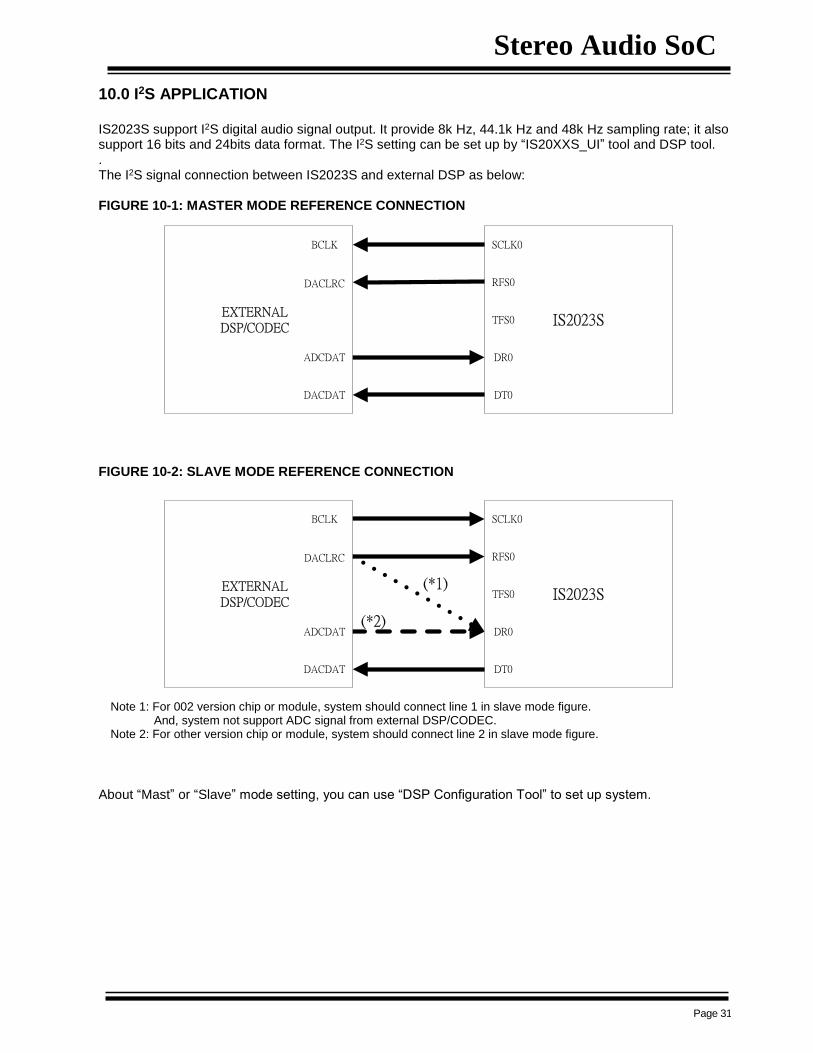
10.0 I2S APPLICATION IS2023S support I2S digital audio signal output. It provide 8k Hz, 44.1k Hz and 48k Hz sampling rate; it also support 16 bits and 24bits data format. The I2S setting can be set up by “IS20XXS_UI” tool and DSP tool. . The I2S signal connection between IS2023S and external DSP as below: FIGURE 10-1: MASTER MODE REFERENCE CONNECTION
FIGURE 10-2: SLAVE MODE REFERENCE CONNECTION
Note 1: For 002 version chip or module, system should connect line 1 in slave mode figure. And, system not support ADC signal from external DSP/CODEC. Note 2: For other version chip or module, system should connect line 2 in slave mode figure.
About “Mast” or “Slave” mode setting, you can use “DSP Configuration Tool” to set up system.
IS2023S
RFS0
TFS0
DR0
SCLK0
DACLRC
BCLK
ADCDAT
DACDAT DT0
EXTERNALDSP/CODEC
IS2023S
RFS0
TFS0
DR0
SCLK0
DACLRC
BCLK
ADCDAT
DACDAT DT0
EXTERNALDSP/CODEC
(*1)
(*2)
Stereo Audio SoC
Page 32
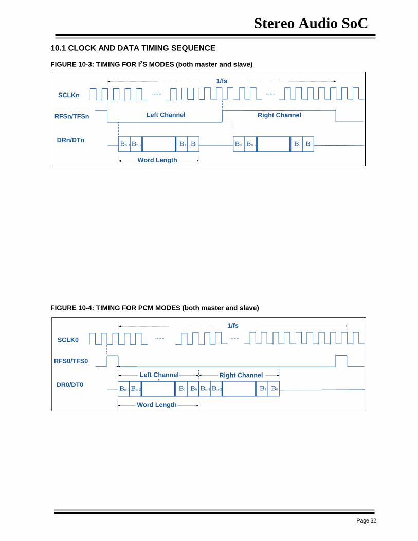
10.1 CLOCK AND DATA TIMING SEQUENCE FIGURE 10-3: TIMING FOR I2S MODES (both master and slave)
FIGURE 10-4: TIMING FOR PCM MODES (both master and slave)
Bn-1
RFSn/TFSn
SCLKn
DRn/DTnBn-2 B1 B0 Bn-1Bn-2 B1 B0
Left Channel Right Channel
1/fs
Word Length
Bn-1
RFS0/TFS0
SCLK0
DR0/DT0Bn-2 B1 B0 Bn-1Bn-2 B1 B0
Left Channel
1/fs
Word Length
Right Channel
Stereo Audio SoC
Page 33
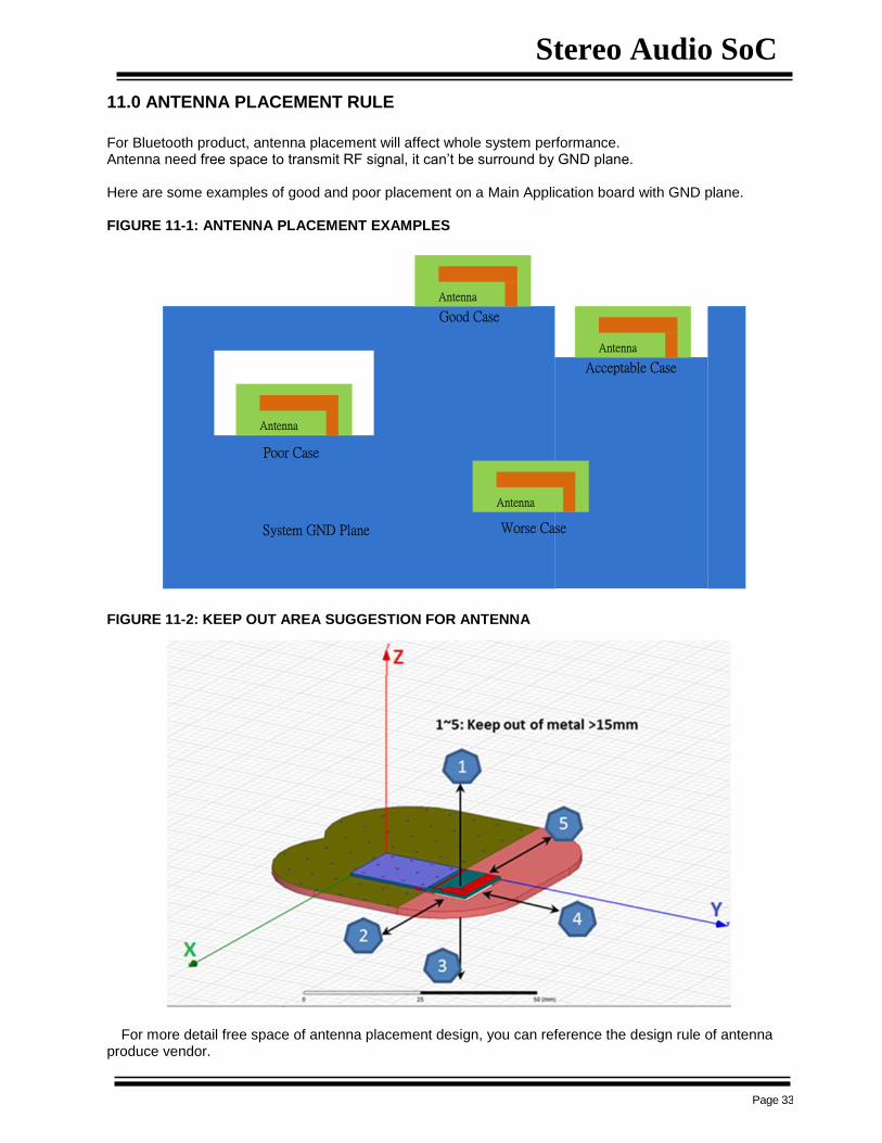
11.0 ANTENNA PLACEMENT RULE
For Bluetooth product, antenna placement will affect whole system performance. Antenna need free space to transmit RF signal, it can’t be surround by GND plane. Here are some examples of good and poor placement on a Main Application board with GND plane. FIGURE 11-1: ANTENNA PLACEMENT EXAMPLES
System GND Plane Worse Case
Poor Case
Good Case
Acceptable Case
Antenna
Antenna
Antenna
Antenna
FIGURE 11-2: KEEP OUT AREA SUGGESTION FOR ANTENNA
For more detail free space of antenna placement design, you can reference the design rule of antenna
produce vendor.
Stereo Audio SoC
Page 34
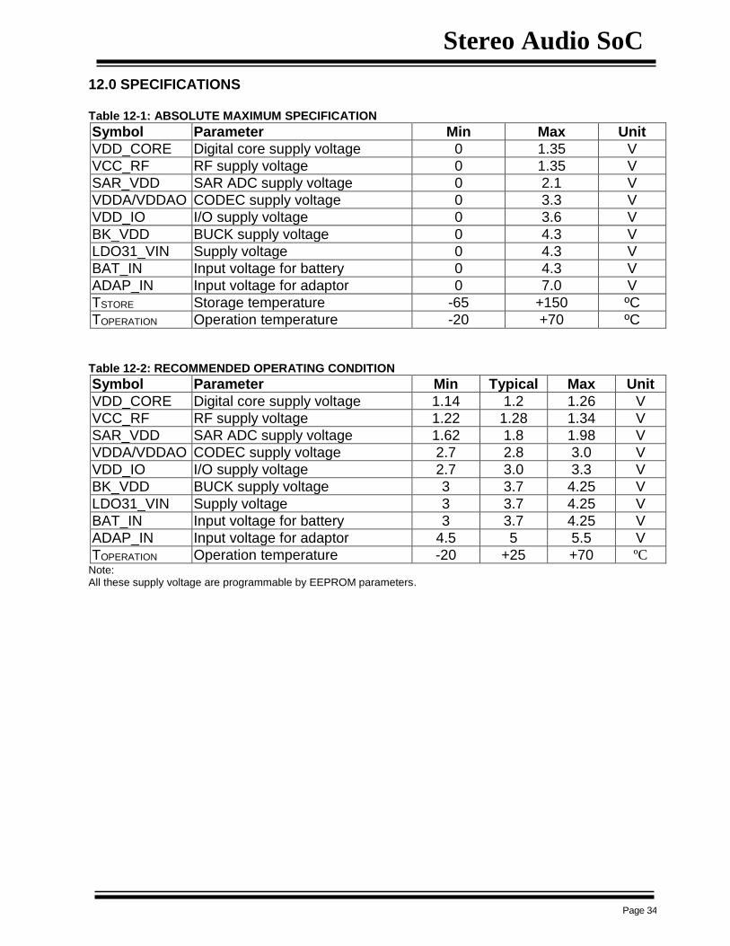
12.0 SPECIFICATIONS Table 12-1: ABSOLUTE MAXIMUM SPECIFICATION
Symbol Parameter Min Max Unit
VDD_CORE Digital core supply voltage 0 1.35 V
VCC_RF RF supply voltage 0 1.35 V
SAR_VDD SAR ADC supply voltage 0 2.1 V
VDDA/VDDAO CODEC supply voltage 0 3.3 V
VDD_IO I/O supply voltage 0 3.6 V
BK_VDD BUCK supply voltage 0 4.3 V
LDO31_VIN Supply voltage 0 4.3 V
BAT_IN Input voltage for battery 0 4.3 V
ADAP_IN Input voltage for adaptor 0 7.0 V
TSTORE Storage temperature -65 +150 ºC
TOPERATION Operation temperature -20 +70 ºC
Table 12-2: RECOMMENDED OPERATING CONDITION
Symbol Parameter Min Typical Max Unit
VDD_CORE Digital core supply voltage 1.14 1.2 1.26 V
VCC_RF RF supply voltage 1.22 1.28 1.34 V
SAR_VDD SAR ADC supply voltage 1.62 1.8 1.98 V
VDDA/VDDAO CODEC supply voltage 2.7 2.8 3.0 V
VDD_IO I/O supply voltage 2.7 3.0 3.3 V
BK_VDD BUCK supply voltage 3 3.7 4.25 V
LDO31_VIN Supply voltage 3 3.7 4.25 V
BAT_IN Input voltage for battery 3 3.7 4.25 V
ADAP_IN Input voltage for adaptor 4.5 5 5.5 V
TOPERATION Operation temperature -20 +25 +70 ºC Note: All these supply voltage are programmable by EEPROM parameters.
Stereo Audio SoC
Page 35
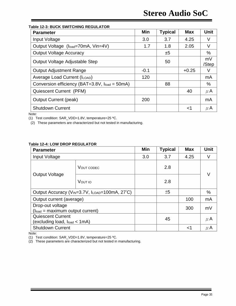
Table 12-3: BUCK SWITCHING REGULATOR
Parameter Min Typical Max Unit
Input Voltage 3.0 3.7 4.25 V
Output Voltage (Iload=70mA, Vin=4V) 1.7 1.8 2.05 V
Output Voltage Accuracy ±5 %
Output Voltage Adjustable Step 50 mV
/Step
Output Adjustment Range -0.1 +0.25 V
Average Load Current (ILOAD) 120 mA
Conversion efficiency (BAT=3.8V, Iload = 50mA) 88 %
Quiescent Current (PFM) 40 μA
Output Current (peak) 200 mA
Shutdown Current <1 μA
Note: (1) Test condition: SAR_VDD=1.8V, temperature=25 ºC.
(2) These parameters are characterized but not tested in manufacturing.
Table 12-4: LOW DROP REGULATOR
Parameter Min Typical Max Unit
Input Voltage 3.0 3.7 4.25 V
Output Voltage
VOUT CODEC 2.8
V
VOUT IO 2.8
Output Accuracy (VIN=3.7V, ILOAD=100mA, 27’C) ±5 %
Output current (average) 100 mA
Drop-out voltage (Iload = maximum output current)
300 mV
Quiescent Current (excluding load, Iload < 1mA)
45 μA
Shutdown Current <1 μA Note: (1) Test condition: SAR_VDD=1.8V, temperature=25 ºC. (2) These parameters are characterized but not tested in manufacturing.
Stereo Audio SoC
Page 36
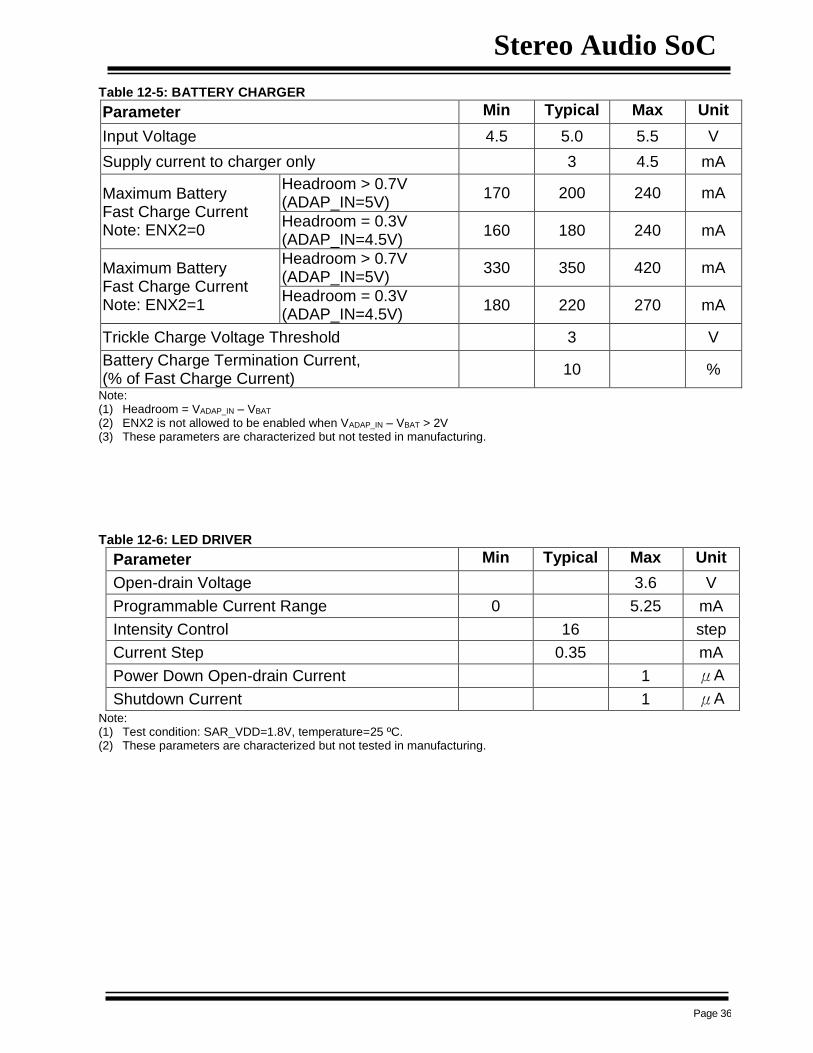
Table 12-5: BATTERY CHARGER
Parameter Min Typical Max Unit
Input Voltage 4.5 5.0 5.5 V
Supply current to charger only 3 4.5 mA
Maximum Battery Fast Charge Current Note: ENX2=0
Headroom > 0.7V (ADAP_IN=5V)
170 200 240 mA
Headroom = 0.3V (ADAP_IN=4.5V)
160 180 240 mA
Maximum Battery Fast Charge Current Note: ENX2=1
Headroom > 0.7V (ADAP_IN=5V)
330 350 420 mA
Headroom = 0.3V (ADAP_IN=4.5V)
180 220 270 mA
Trickle Charge Voltage Threshold 3 V
Battery Charge Termination Current, (% of Fast Charge Current)
10 %
Note: (1) Headroom = VADAP_IN – VBAT (2) ENX2 is not allowed to be enabled when VADAP_IN – VBAT > 2V (3) These parameters are characterized but not tested in manufacturing.
Table 12-6: LED DRIVER
Parameter Min Typical Max Unit
Open-drain Voltage 3.6 V
Programmable Current Range 0 5.25 mA
Intensity Control 16 step
Current Step 0.35 mA
Power Down Open-drain Current 1 μA
Shutdown Current 1 μA Note: (1) Test condition: SAR_VDD=1.8V, temperature=25 ºC. (2) These parameters are characterized but not tested in manufacturing.
Stereo Audio SoC
Page 37
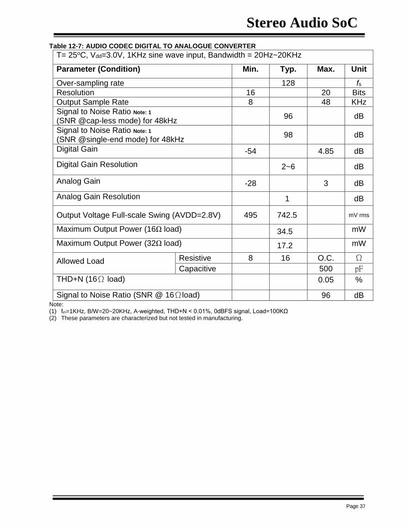
Table 12-7: AUDIO CODEC DIGITAL TO ANALOGUE CONVERTER
T= 25oC, Vdd=3.0V, 1KHz sine wave input, Bandwidth = 20Hz~20KHz
Parameter (Condition) Min. Typ. Max. Unit
Over-sampling rate 128 fs
Resolution 16 20 Bits
Output Sample Rate 8 48 KHz
Signal to Noise Ratio Note: 1 (SNR @cap-less mode) for 48kHz
96 dB
Signal to Noise Ratio Note: 1 (SNR @single-end mode) for 48kHz
98 dB
Digital Gain -54 4.85 dB
Digital Gain Resolution 2~6 dB
Analog Gain -28 3 dB
Analog Gain Resolution 1 dB
Output Voltage Full-scale Swing (AVDD=2.8V) 495 742.5
mV rms
Maximum Output Power (16Ω load) 34.5 mW
Maximum Output Power (32Ω load) 17.2 mW
Allowed Load Resistive 8 16 O.C. Ω
Capacitive 500 pF
THD+N (16Ω load) 0.05 %
Signal to Noise Ratio (SNR @ 16Ωload) 96 dB Note: (1) fin=1KHz, B/W=20~20KHz, A-weighted, THD+N < 0.01%, 0dBFS signal, Load=100KΩ (2) These parameters are characterized but not tested in manufacturing.
Stereo Audio SoC
Page 38
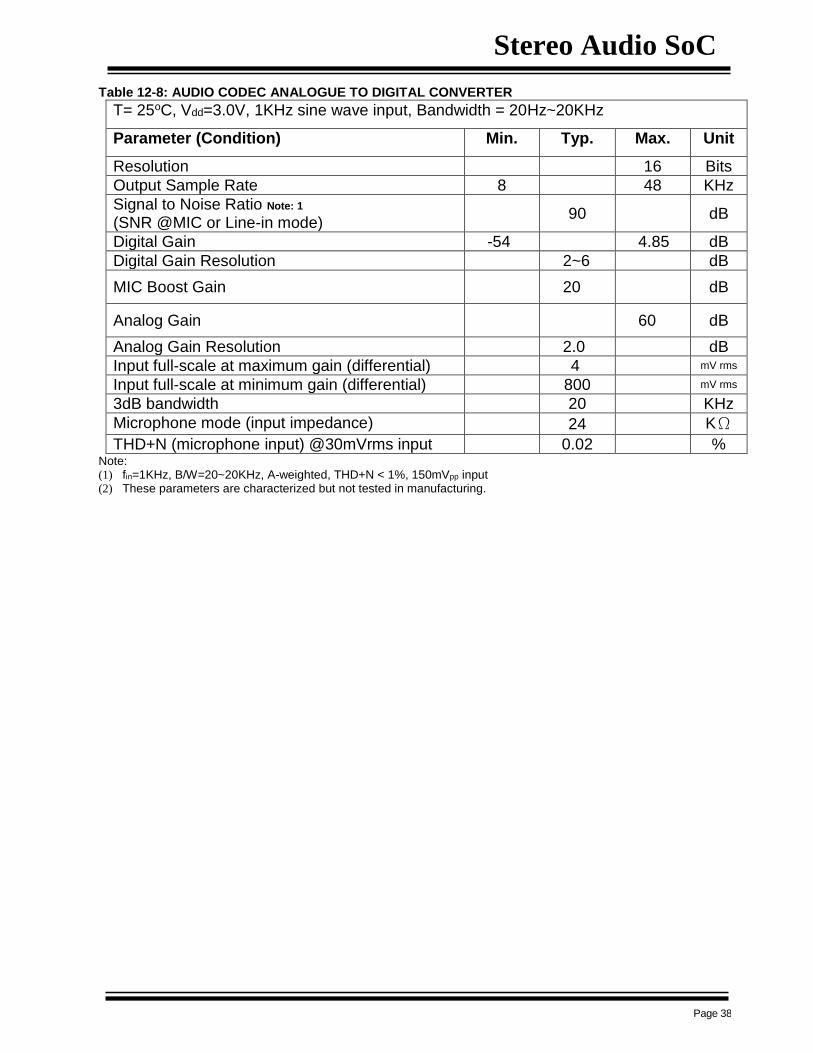
Table 12-8: AUDIO CODEC ANALOGUE TO DIGITAL CONVERTER
T= 25oC, Vdd=3.0V, 1KHz sine wave input, Bandwidth = 20Hz~20KHz
Parameter (Condition) Min. Typ. Max. Unit
Resolution 16 Bits
Output Sample Rate 8 48 KHz
Signal to Noise Ratio Note: 1
(SNR @MIC or Line-in mode) 90 dB
Digital Gain -54 4.85 dB
Digital Gain Resolution 2~6 dB
MIC Boost Gain 20 dB
Analog Gain 60 dB
Analog Gain Resolution 2.0 dB
Input full-scale at maximum gain (differential) 4 mV rms
Input full-scale at minimum gain (differential) 800 mV rms
3dB bandwidth 20 KHz
Microphone mode (input impedance) 24 KΩ
THD+N (microphone input) @30mVrms input 0.02 % Note: (1) fin=1KHz, B/W=20~20KHz, A-weighted, THD+N < 1%, 150mVpp input (2) These parameters are characterized but not tested in manufacturing.
Stereo Audio SoC
Page 39
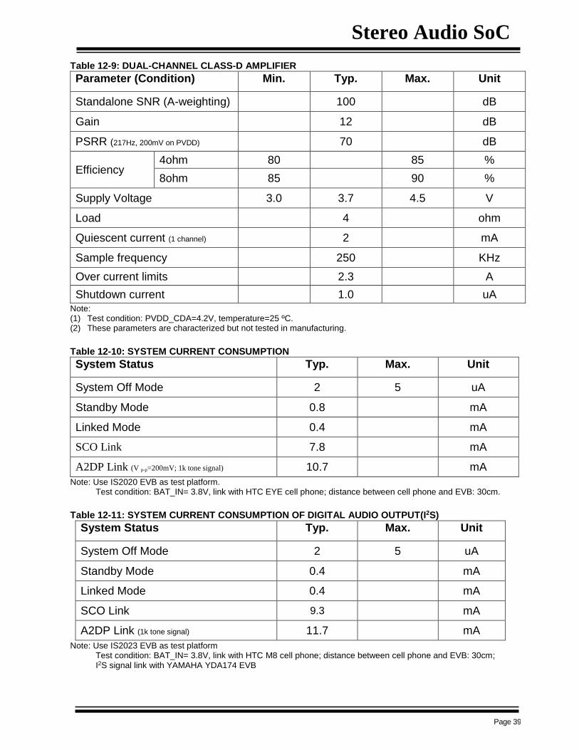
Table 12-9: DUAL-CHANNEL CLASS-D AMPLIFIER
Parameter (Condition) Min. Typ. Max. Unit
Standalone SNR (A-weighting) 100 dB
Gain 12 dB
PSRR (217Hz, 200mV on PVDD) 70 dB
Efficiency 4ohm 80 85 %
8ohm 85 90 %
Supply Voltage 3.0 3.7 4.5 V
Load 4 ohm
Quiescent current (1 channel) 2 mA
Sample frequency 250 KHz
Over current limits 2.3 A
Shutdown current 1.0 uA Note: (1) Test condition: PVDD_CDA=4.2V, temperature=25 ºC. (2) These parameters are characterized but not tested in manufacturing.
Table 12-10: SYSTEM CURRENT CONSUMPTION
System Status Typ. Max. Unit
System Off Mode 2 5 uA
Standby Mode 0.8 mA
Linked Mode 0.4 mA
SCO Link 7.8 mA
A2DP Link (V p-p=200mV; 1k tone signal) 10.7 mA
Note: Use IS2020 EVB as test platform. Test condition: BAT_IN= 3.8V, link with HTC EYE cell phone; distance between cell phone and EVB: 30cm.
Table 12-11: SYSTEM CURRENT CONSUMPTION OF DIGITAL AUDIO OUTPUT(I2S)
System Status Typ. Max. Unit
System Off Mode 2 5 uA
Standby Mode 0.4 mA
Linked Mode 0.4 mA
SCO Link 9.3 mA
A2DP Link (1k tone signal) 11.7 mA
Note: Use IS2023 EVB as test platform Test condition: BAT_IN= 3.8V, link with HTC M8 cell phone; distance between cell phone and EVB: 30cm; I2S signal link with YAMAHA YDA174 EVB
Stereo Audio SoC
Page 40
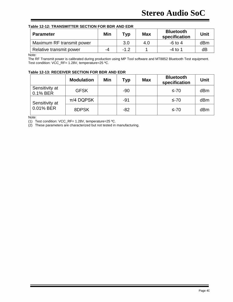
Table 12-12: TRANSMITTER SECTION FOR BDR AND EDR
Parameter Min Typ Max Bluetooth
specification Unit
Maximum RF transmit power 3.0 4.0 -6 to 4 dBm
Relative transmit power -4 -1.2 1 -4 to 1 dB Note: The RF Transmit power is calibrated during production using MP Tool software and MT8852 Bluetooth Test equipment. Test condition: VCC_RF= 1.28V, temperature=25 ºC. Table 12-13: RECEIVER SECTION FOR BDR AND EDR
Modulation Min Typ Max Bluetooth
specification Unit
Sensitivity at 0.1% BER
GFSK -90 ≤-70 dBm
Sensitivity at 0.01% BER
π/4 DQPSK -91 ≤-70 dBm
8DPSK -82 ≤-70 dBm
Note: (1) Test condition: VCC_RF= 1.28V, temperature=25 ºC. (2) These parameters are characterized but not tested in manufacturing.
Stereo Audio SoC
Page 41
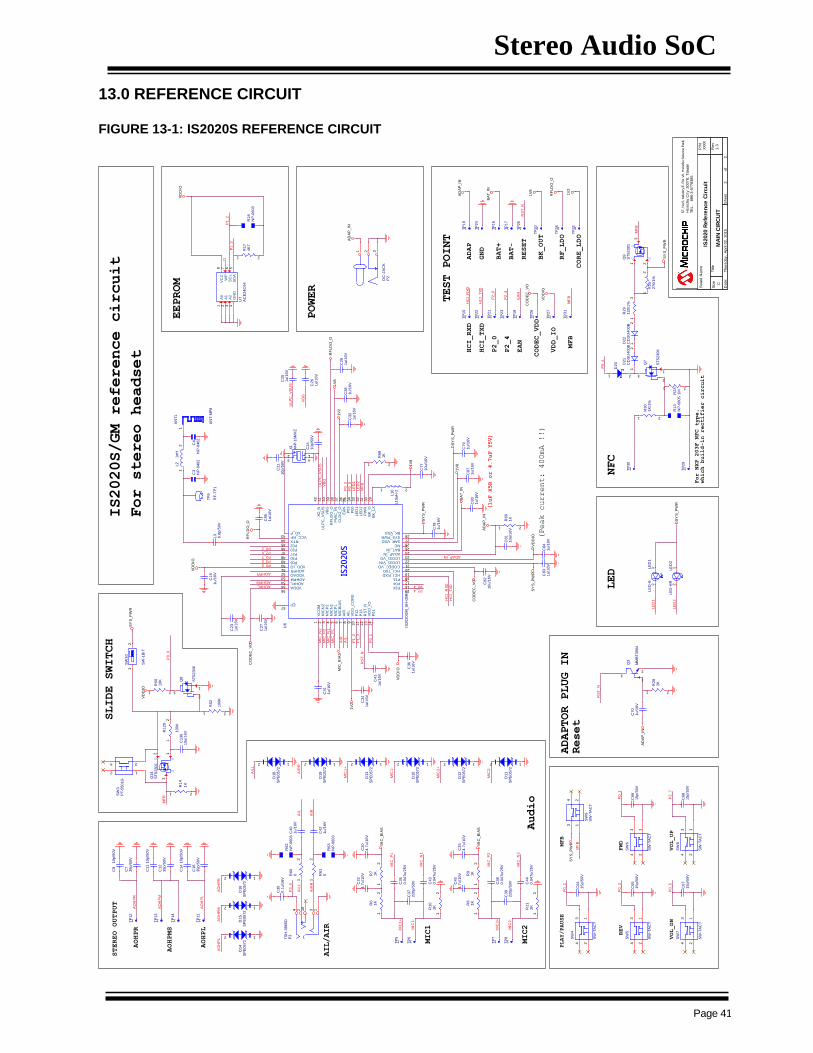
13.0 REFERENCE CIRCUIT FIGURE 13-1: IS2020S REFERENCE CIRCUIT
LED
AO
HP
MA
OH
PR
R6
81K
1 2
IS2
02
0S
U6
IS2
02
0G
M_
SH
+2
MIC
AOHPR52
AOHPL55 VDDA56
VC
OM
1
MIC
N1
4
MIC
P1
5
MIC
BIA
S6
AIR
7
VD
D_
IO13
RS
T_
N12
P03
35
P12
10
P13
11
P2748
HCI_TXD19HCI_RXD18
XO_P43
XO
_N
42
UL
PC
_V
SU
S41
P0416
VB
G40
RF
LD
O_
O39
PM
IC_
IN38
CL
DO
_O
37
EA
N36
NC25
VD
D_
CO
RE
9
P2415
P2047
P3049
P0246
P01
14
VDD_IO51
RTX45
VCC_RF44
P00
34
EP57
VDDAO53 AOHPM54
MIC
N2
2
MIC
P2
3
P1517
AIL
8
P0550 CODEC_VO
20
LDO31_VIN21
LDO31_VO22
ADAP_IN23
BAT_IN24
SAR_VDD26
SYS_PWR27
BK_VDD28
BK
_LX
29
BK
_O
30
PW
R31
LE
D1
33
LE
D2
32
CO
DE
C_
VO
1V
8
MIC
_N
1
MIC
_P
1
C2
31
u/1
6V
C3
72
20
p/5
0VC3
50
.04
7u
/25
V
C2
71
u/1
6V
R1
02K
12
C4
30
.04
7u
/25
V
Bo
ard
Na
me
Siz
eT
itle
Re
v
Da
te:
Sheet
of
P/N
MA
IN C
IRC
UIT
1.3
IS2020 R
efe
ren
ce
Cir
cu
it
C
22
Th
urs
da
y,
Ap
ril 0
2,
20
15
XX
XX
5F
, N
o.5
, In
dustr
y E
. R
d. V
II, H
sin
chu S
cie
nce P
ark
,
Hsin
ch
u C
ity
30
07
8,
Ta
iwa
nT
EL
.
88
6-3
-57
78
38
5
TP
5 1
TP
6 1
MIC
_B
IAS
MIC
1+
MIC1M
IC1
-
C2
04
.7u
/10
VR
61K
12
R7
1K
12
C2
24
.7u
/10
V
TP
11
1
AOHPL
AOHPR
AOHPMS
TP
13
1T
P1
21
TP
14
1
MF
B
TP
28 1
RF_LDO
RF
LD
O_
O
LE
D2
LE
D1
LE
D1
LE
D-B
12
LE
D2
LE
D-H
R1
2
L10
L1
0u
H-2
1 2
SY
S_
PW
R
P0_4
Q7
STS
23
06
31
2
GD
SQ9
STS
23
01
13
2
R2
31M
1 2
D2
0
21
D2
2C
DS
U4
00
B1
2
D2
1C
DS
U4
00
B1
2
R2
91
20
/1%
12
R2
52
70
/1%
12
R1
3N
P-0
80
5
R3
01
K/1
%
1 2
TP
29
1
MF
B
TP
30
1
D1
2S
PE
0572
2 1
P0_3
P0_2
FWD
P0_5
C6
61
5p
/50
V
VOL_UP
SW
6
SW
-TA
CT
12
34
P2_7
SW
8
SW
-TA
CT
12
34
C6
81
5p
/50
V
C6
41
5p
/50
V
VOL_DN
REV
PLAY/PAUSE
P0_3
P0_0
SW
4
SW
-TA
CT
12
34
C6
51
5p
/50
V
SW
5
SW
-TA
CT
12
34
C2
81
u/1
6V
RF
LD
O_
O
C6
71
5p
/50
V
C3
21
u/1
6V
C2
91
u/1
6V
SW
7
SW
-TA
CT
12
34
P0_1
UL
PC
_V
SU
SV
BG
UL
PC
_V
SU
S
VB
G
D1
0S
PE
0572
2 1
C2
51
u/1
6V
C2
61
u/1
6V
NFC
LE
D1
1V
21V
8
LE
D2
MIC
2+
C7
71
0u
/16
V
1V
2S
YS
_P
WR
MF
B
SW
9S
W-T
AC
T
12
34
RS
T_
N
AD
AP
_IN
R2
82K
1 2
C7
01
u/1
6V
Q3
MM
BT3
90
4
32
1
TP
32 1
D1
3S
PE
0572
2 1
MIC
1+
BAT-
BK_OUT
RS
T_
NRESET
HCI_TXD
TEST POINT
GND
ADAP
For NXP 203F NFC type,
which build-in rectifier circuit
HCI_RXD
P2_0
P2_4
EA
N
HC
I_TX
D
HC
I_R
XD
TP
15
1
CODEC_VDD
AD
AP
_IN
TP
16
1
TP
18
1
TP
20 1
TP
19
1
TP
17
1
TP
23
1
TP
22
1
TP
21
1
TP
25
1
TP
24
1
TP
26
1
BA
T_
IN
1V
8
P2_0
BAT+
CO
DE
C_
VO
TP
27
1
VDD_IO
P2_4
EAN
VD
DIO
VD
DIO
C3
11
u/1
6V
AIL
MIC
_N
2M
IC_
P2
AIR
1V
2P
1_2
MIC
_N
1M
IC_
P1
D1
8S
PE
0572
2 1
MIC
_B
IAS
C3
41
u/1
6V
P1_3
RS
T_
N
C4
11
u/1
6V
C3
61
u/1
6V
CORE_LDO
MIC
1-
VD
DIO
RF
LD
O_
O
C1
91
u/1
6V
L3
6.8
p/5
0V
P0_5
P0_2P2_0P2_7
C8
61
u/1
6V
AO
HP
L
P3_0
D1
9S
PE
0572
2 1
MIC
_N
2
MIC
_P
2
C3
92
20
p/5
0VC3
80
.04
7u
/25
V
R1
12K
12
C4
40
.04
7u
/25
V
TP
7 1
TP
8 1
MIC
2-
MIC
2+
MIC2
MIC
_B
IAS
C3
34
.7u
/10
VR
81K
12
AD
AP
_IN
R9
1K
12
C4
54
.7u
/10
V
P2
DC
-JA
CK
1 2 3
C8
11
0u
/16
V
AIR
R
POWER
AO
HP
R
AOHPR
(1uF X5R or 4.7uF Y5V)
AIL
L
Audio
AD
AP
_IN
C2
11
0p
/50
V
X1
X4
P-1
6M
HZ
41
32
C2
41
0p
/50
V
AOHPMAOHPL
D1
1S
PE
0572
2 1
P0_1
IS2020S/GM reference circuit
MFB
TP
9
RF
-TP
1
L2
1nH
12
AN
T1
AN
T-M
P8
1
C3
NP
-04
02
C4
NP
-04
02
U7
AC
E2
4C
64
A0
1
A1
2
A2
3
GN
D4
SD
A5
SC
L6
WP
7V
CC
8
P0_0
R1
4
1K
1 2
R5
2
100K
1 2
R1
29
100K
12
Q8
STS
23
06
31
2
C1
36
10
u/1
6V
SW
10
SW
-1B
IT
12
SW
3P
T-5
50
1G
12
34
GD
S
Q14
STS
23
01
13
2R
50
10K
1 2
SY
S_
PW
R
VD
DIO
SLIDE SWITCH
C3
00
.1u
/16
V
P3
TS
H-3
86
5D
4 32 10
1
P3_0
MIC
2-
ADAPTOR PLUG IN
Reset
D1
4S
PE
0572
2 1
For stereo headset
R6
00
12
AIL/AIR
R6
3N
P-0
60
3
R6
10
12
R6
2N
P-0
60
3
AIL
L
AIR
R
C4
01
u/1
6V
C4
21
u/1
6V
AIL
AIR
VD
DIO
R1
8N
P-0
60
3
P1_2
P1_3
R1
74K
7
1 2
EEPROM
C1
11
0p
/50
V
C1
41
0p
/50
V
STEREO OUTPUT
AO
HP
M
C7
39
p/5
0V
C1
63
9p
/50
V
C1
23
9p
/50
V
C8
10
p/5
0V
P0_4P2_4
HC
I_TX
DH
CI_
RX
D C8
21
0u
/16
V
MF
B
1V
8
ADAP_IN
D1
5S
PE
0572
2 1
C8
71
u/1
6V
SY
S_
PW
R
BA
T_
IN
C8
41
u/1
6V
(Peak current: 400mA !!)
CO
DE
C_
VO
C8
01
u/1
6V
C8
31
u/1
6V
TP
31
1
C7
91
u/1
6V
MFB
SY
S_
PW
R
SY
S_
PW
RV
DD
IO
MF
B
C7
81
u/1
6V R6
91K
1 2
D1
6S
PE
0572
2 1
SY
S_
PW
R
AO
HP
L
Stereo Audio SoC
Page 42
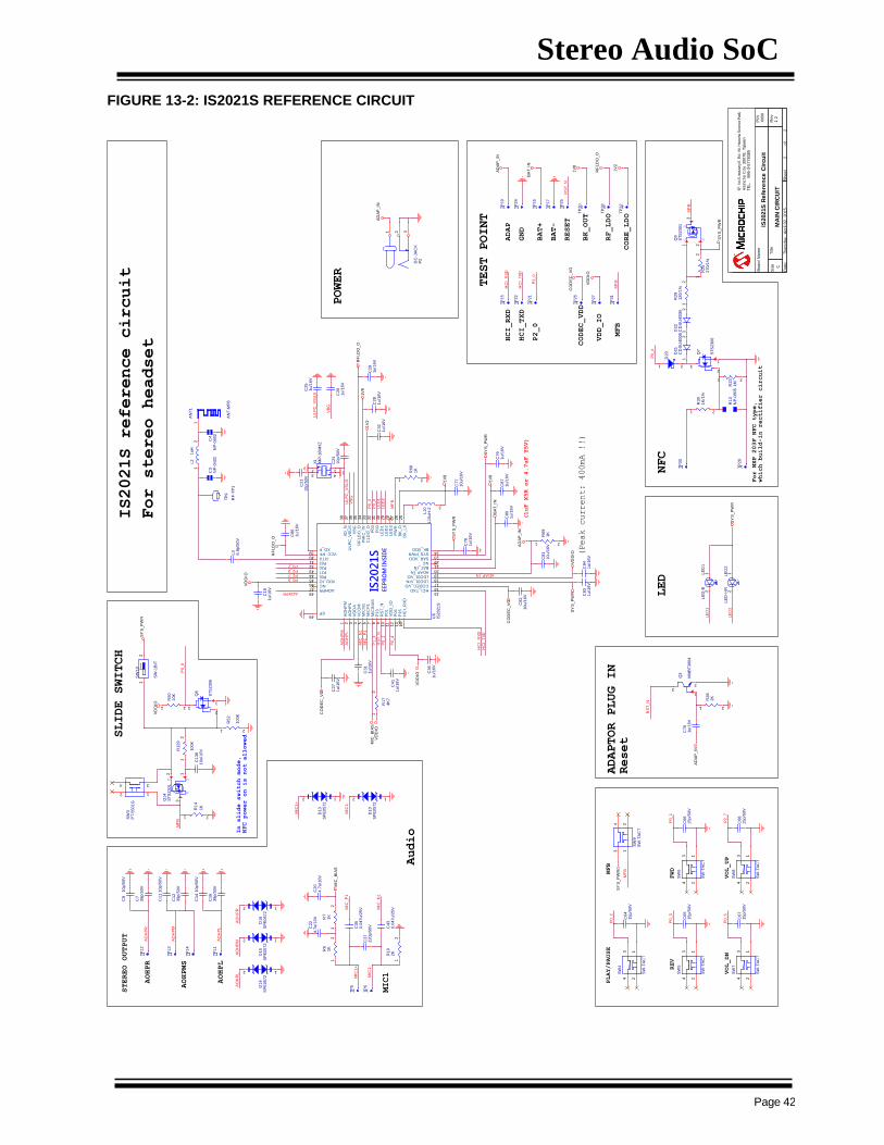
FIGURE 13-2: IS2021S REFERENCE CIRCUIT
LED
AO
HP
M
C2
11
0p
/50
V
C2
41
0p
/50
V
X1
X4
P-1
6M
HZ
41
32
AO
HP
R
R6
81K
1 2
1V
8
MIC
_N
1
MIC
_P
1
C3
72
20
p/5
0VC3
50
.04
7u
/25
V
R1
02K
12
C4
30
.04
7u
/25
V
TP
5 1
TP
6 1
MIC
_B
IAS
MIC
1+
MIC1M
IC1
-
C2
04
.7u
/10
VR
61K
12
R7
1K
12
C2
24
.7u
/10
V
TP
11
1
AOHPL
AOHPR
AOHPMS
TP
13
1
TP
12
1T
P1
41
MF
B
TP
28 1
RF_LDO
RF
LD
O_
O
LE
D2
LE
D1
LE
D1
LE
D-B
12
LE
D2
LE
D-H
R1
2
HC
I_TX
DH
CI_
RX
D
L10
L1
0u
H-2
1 2
P0_0
LE
D2
LE
D1
P0_3
SY
S_
PW
R
P0_4
Q7
STS
23
06
31
2
GD
SQ9
STS
23
01
13
2
R2
31M
1 2
D2
0
21
D2
2C
DS
U4
00
B1
2
D2
1C
DS
U4
00
B1
2
R2
91
20
/1%
12
R2
52
70
/1%
12
R1
3N
P-0
80
5
R3
01
K/1
%
1 2
TP
29
1
MF
B
TP
30
1
P0_3
P0_2
FWD
P0_5
C6
61
5p
/50
V
VOL_UP
SW
6
SW
-TA
CT
12
34
P2_7
SW
8
SW
-TA
CT
12
34
C6
81
5p
/50
V
C6
41
5p
/50
V
VOL_DN
REV
PLAY/PAUSE
SW
4
SW
-TA
CT
12
34
C6
51
5p
/50
V
AO
HP
MA
OH
PL
SW
5
SW
-TA
CT
12
34
C2
81
u/1
6V
RF
LD
O_
O
C6
71
5p
/50
V
C3
21
u/1
6V
C2
91
u/1
6V
SW
7
SW
-TA
CT
12
34
P0_1
UL
PC
_V
SU
SV
BG
UL
PC
_V
SU
S
VB
G
D1
0S
PE
0572
2 1
C2
51
u/1
6V
C2
61
u/1
6V
NFC
1V
21V
8
C7
71
0u
/16
V
1V
2S
YS
_P
WR
MF
B
SW
9S
W-T
AC
T
12
34
RS
T_
N
AD
AP
_IN
R2
82K
1 2
C7
01
u/1
6V
Q3
MM
BT3
90
4
32
1
TP
32 1
D1
3S
PE
0572
2 1
MIC
1+
BAT-
BK_OUT
RS
T_
NRESET
HCI_TXD
TEST POINT
GND
ADAP
For NXP 203F NFC type,
which build-in rectifier circuit
HCI_RXD
P2_0
HC
I_TX
D
HC
I_R
XD
TP
15
1
CODEC_VDD
AD
AP
_IN
TP
16
1
TP
20 1
TP
19
1
TP
17
1
TP
22
1
TP
21
1
TP
25
1
TP
24
1
TP
26
1
BA
T_
IN
1V
8
P2_0
BAT+
CO
DE
C_
VO
TP
27
1
VDD_IO
VD
DIO
MIC
_N
1M
IC_
P1
MIC
_B
IAS
CORE_LDO
C3
11
u/1
6V
MIC
1-
C8
11
0u
/16
VAD
AP
_IN
C8
21
0u
/16
V
1V
8
ADAP_IN
L3
6.8
p/5
0V
C8
71
u/1
6V
SY
S_
PW
R
AO
HP
L
(Peak current: 400mA !!)
BA
T_
IN
C8
41
u/1
6V
CO
DE
C_
VO
C8
01
u/1
6V
C8
31
u/1
6V
SY
S_
PW
R
SY
S_
PW
RV
DD
IO
C7
81
u/1
6V
C7
91
u/1
6V
R6
91K
1 2
AD
AP
_IN
P2
DC
-JA
CK
1 2 3
(1uF X5R or 4.7uF Y5V)
CO
DE
C_
VO
C2
71
u/1
6V
POWER
AO
HP
R
AOHPR
Audio
VD
DIO
C1
91
u/1
6V IS
20
21
SE
EP
RO
M I
NS
IDE
U6
IS2
02
1S
AOHPR48
AO
HP
L2
VD
DA
3
VC
OM
4
MIC
N1
5
MIC
P1
6
MIC
BIA
S7
VD
D_
IO11
RS
T_
N9
P03
32
P13
8
P2744
HCI_TXD15
XO_P39
XO
_N
38
UL
PC
_V
SU
S37
P04
12
VB
G36
RF
LD
O_
O35
PM
IC_
IN34
CL
DO
_O
33
NC21
NC47
P2043
P00
31
P0242
P01
10
VDD_IO46
RTX41
VCC_RF40
EP49 A
OH
PM
1
P15
13
P0545
CODEC_VO16
LDO31_VIN17
LDO31_VO18
ADAP_IN19
BAT_IN20
SAR_VDD22
SYS_PWR23
BK_VDD24
BK
_LX
25
BK
_O
26
PW
R27
LE
D1
30
LE
D2
29
LE
D3
28
HC
I_R
XD
14
R1
74K
7
12
IS2021S reference circuit
MFB
TP
9
RF
-TP
1
L2
1nH
12
AN
T1
AN
T-M
P8
1
C3
NP
-04
02
C4
NP
-04
02
VD
DIO
P1_3
RS
T_
N
C3
61
u/1
6V
C4
11
u/1
6V
P0_1
Bo
ard
Na
me
Siz
eT
itle
Re
v
Da
te:
Sheet
of
P/N
MA
IN C
IRC
UIT
1.2
IS2021S
Re
fere
nce
Cir
cu
it
C
22
Th
urs
da
y,
Ap
ril 0
2,
20
15
XX
XX
5F
, N
o.5
, In
dustr
y E
. R
d. V
II, H
sin
chu S
cie
nce P
ark
,
Hsin
ch
u C
ity
30
07
8,
Ta
iwa
nT
EL
.
88
6-3
-57
78
38
5
P0_0
R1
4
1K
1 2
R5
2
100K
1 2
R1
29
100K
12
Q8
STS
23
06
31
2
C1
36
10
u/1
6V
SW
10
SW
-1B
IT
12
SW
3P
T-5
50
1G
12
34
GD
S
Q14
STS
23
01
13
2R
50
10K
1 2
SY
S_
PW
R
VD
DIO
SLIDE SWITCH
P2_7P0_5
P0_2P2_0
VD
DIO
ADAPTOR PLUG IN
Reset
D1
4S
PE
0572
2 1
In slide switch mode,
NFC power on is not allowed
For stereo headset
P0_4
C1
11
0p
/50
V
C1
41
0p
/50
V
STEREO OUTPUT
AO
HP
M
C7
39
p/5
0V
RF
LD
O_
O
C1
63
9p
/50
V
C8
61
u/1
6V
C1
23
9p
/50
V
C8
10
p/5
0V
MF
B
D1
5S
PE
0572
2 1
TP
31
1
MFB
MF
B
D1
6S
PE
0572
2 1
SY
S_
PW
R
AO
HP
L
Stereo Audio SoC
Page 43
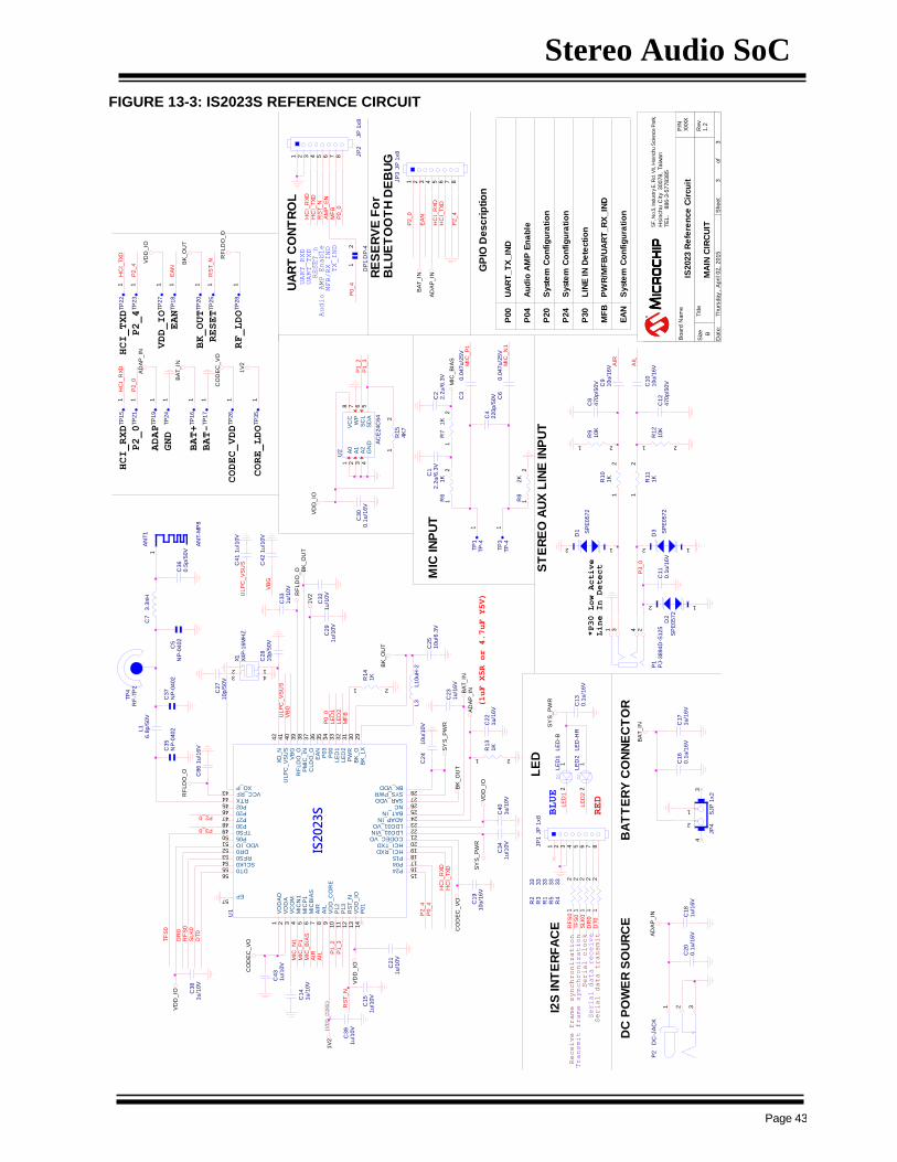
FIGURE 13-3: IS2023S REFERENCE CIRCUIT
C5
NP
-0402
C7
3.3
nH
C29
1u/1
0V
C36
0.5
p/5
0V
AD
AP
_IN
C32
1u/1
0V
C20
0.1
u/1
6V
C38
1u/1
0V
C41
1u/1
0V
EA
N
P00
C43
1u/1
0V
Syst
em
Co
nfi
gu
rati
on
LIN
E I
N D
ete
cti
on
P20
P24
PW
R/M
FB
/UA
RT
_R
X_IN
D
Syst
em
Co
nfi
gu
rati
on
Syst
em
Co
nfi
gu
rati
on
P30
GP
IO D
es
cri
pti
on
MF
B
Receive frame synchronization
BK
_O
UT
Transmit frame synchronization
L1
6.8
p/5
0V
BA
T_IN
P0_4
Serial clock
P1
PJ-3
894D
-S12523 41
AIL
AIR
D2
SP
E0572
2 1
ST
ER
EO
AU
X L
INE
IN
PU
T
*P30 Low Active
Line In Detect
Serial data receive
D3 SP
E0572
2 1
D1 SP
E0572
2 1
P3_0
C8
470p/5
0V
C12
470p/5
0V
C11
0.1
u/1
6V
C10
10u/1
6V
C9
10u/1
6V
R9
10K
1 2
R12
10K
1 2
C35
NP
-0402
R11
1K
12
R10
1K
12
Serial data transmit
AD
AP
_IN
AM
P_E
N
JP
2JP
1x8
1 2 3 4 5 6 7 8
C42
1u/1
0V
MF
B
R14
1K
1 2
C24
10u/1
0V
SY
S_P
WR
ULP
C_V
SU
S
VB
G
C33
1u/1
0V
HC
I_TXD
HC
I_R
XD
LE
D2
LE
D1
C17
1u/1
6V
DR
0S
LK
0
R2
33
12
TF
S0
RF
S0
DT0
RS
T_N
C18
1u/1
6V
P3_0
P2_0
Board
Nam
e
Siz
eTitle
Rev
Date
:S
heet
of
P/N
MA
IN C
IRC
UIT
1.2
IS2023 R
efe
ren
ce
Cir
cu
it
B
33
Thurs
day
, A
pril 02,
2015
XXXX
5F
, N
o.5
, In
dustr
y E
. R
d. V
II, H
sin
chu S
cie
nce P
ark
,
Hsin
chu C
ity
30078,
Taiw
an
TE
L.
886-3
-5778385
RF
LD
O_O
C86
1u/1
6V
C37
NP
-0402
DP
1D
P-42
1
P0_0
C14
1u/1
0V
Audio AMP Enable
P2
DC
-JA
CK
1 2 3I2S
IN
TE
RF
AC
E
MIC
_N
1
MIC
_P
1
R7
1K
12
C1
2.2
u/6
.3V
C2
2.2
u/6
.3V
R6
1K
12
C4
220p/5
0V
R8
2K
12
MIC
_B
IAS
BA
TT
ER
Y C
ON
NE
CT
OR
MF
B
JP
3JP
1x8
1 2 3 4 5 6 7 8
DR
0R
FS
0S
LK
0D
T0
TF
S0
P0_0
IS2
02
3S
U1
EP57
TFS050
DT056
DR053
SCLK055
RFS054
P2748
P2047
P3049
P01
14
VDD_IO52
RTX45
VCC_RF44
XO_P43
P03
35
P2415
P0416
HCI_RXD18
HCI_TXD19
NC25
CODEC_VO20
LDO31_VIN21
LDO31_VO22
ADAP_IN23
BAT_IN24
SAR_VDD26
SYS_PWR27
BK_VDD28
BK
_LX
29
XO
_N
42
ULP
C_V
SU
S41
P1517
VB
G40
RF
LD
O_O
39
PM
IC_IN
38
CLD
O_O
37
EA
N36
P0551
P00
34
LE
D1
33
LE
D2
32
PW
R31
BK
_O
30
VD
DA
O1
AIR
7
AIL
8
VD
DA
2
VC
OM
3
MIC
N1
4
MIC
P1
5
MIC
BIA
S6
VD
D_C
OR
E9
P12
10
P13
11
RS
T_N
12
VD
D_IO
13
P0246
C39
1u/1
0V
DC
PO
WE
R S
OU
RC
E
C16
0.1
u/1
6V
UA
RT
_T
X_IN
D
CO
DE
C_V
O
TP
1TP
-4
1C
19
10u/1
6V
LE
D
TX_IND
C3
0.0
47u/2
5V
TP
3TP
-4
1
CO
DE
C_V
O
C6
0.0
47u/2
5V
JP
1JP
1x8
1 2 3 4 5 6 7 8
MIC
IN
PU
T
R15
4K
7
12
C30
0.1
u/1
6V
VD
D_IO
R3
33
12
P1_3
P1_2
R1
33
12
R5
33
12
BK
_O
UT
AIL
MIC
_B
IAS
AIR
1V
2
R4
33
12
MFB/RX_IND
VD
D_IO
C15
1u/1
0V
VD
D_IO
(1uF X5R or 4.7uF Y5V)
SY
S_P
WR
RESET_n
JP
4S
JP
1x2
2
1
34
UART_RXD
C21
1u/1
0V
C27
10p/5
0V
X1
X4P
-16M
HZ
41
32
C28
10p/5
0V
UA
RT
CO
NT
RO
L
C23
1u/1
6V
RF
LD
O_O
R13
1K
1 2
AD
AP
_IN
C22
1u/1
6V
RS
T_N
BA
T_IN
RE
SE
RV
E F
or
BL
UE
TO
OT
H D
EB
UG
ULP
C_V
SU
SV
BG
LE
D2
C13
0.1
u/1
6V
RED
BLUE
LE
D1
LE
D-B
12
LE
D2
LE
D-H
R1
2
CORE_LDO
BK
_O
UT
1V
2
TP
35
1
RF
LD
O_O
SY
S_P
WR
RS
T_N
TP
28
1
C34
1u/1
0V
BAT-
RF_LDO
LE
D1
HCI_RXD
HCI_TXD
BK_OUT
GND
ADAP
RESET
EA
N
HC
I_TXD
HC
I_R
XD
CODEC_VDD
P2_0
P2_4
TP
18
1
TP
15
1
AD
AP
_IN
TP
19
1
TP
16
1
TP
17
1
TP
21
1TP
23
1
TP
20
1
TP
24
1
TP
22
1
P1_3
P1_2
TP
26
1
TP
25
1
BA
T_IN
P2_0
CO
DE
C_V
O
P2_4
BAT+
VD
D_IO
TP
27
1
EAN
VDD_IO
BA
T_IN
UART_TXD
C40
1u/1
0V
C25
10u/6
.3V
L3
L10uH
-2
P2_0
BK
_O
UT
VD
D_IO
(VDD_CORE)
1V
2
P2_4
HC
I_TXD
HC
I_R
XD
MIC
_P
1
HC
I_R
XD
EA
N
P04
HC
I_TXD
Au
dio
AM
P E
na
ble
P2_4
U2
AC
E24C
64
A0
1
A1
2
A2
3
GN
D4
SD
A5
SC
L6
WP
7V
CC
8
P0_4
MIC
_N
1
AN
T1
AN
T-M
P8
1
TP
4R
F-T
P2
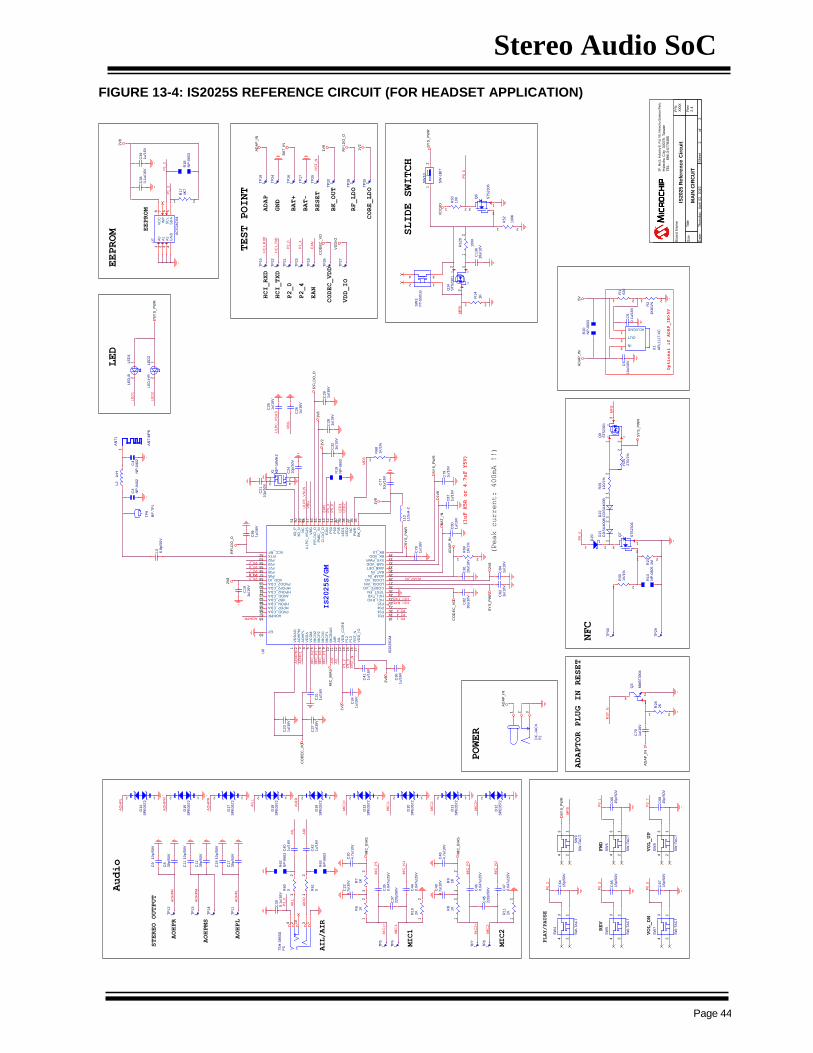
Stereo Audio SoC
Page 44
FIGURE 13-4: IS2025S REFERENCE CIRCUIT (FOR HEADSET APPLICATION)
Board
Nam
e
Siz
eTitle
Rev
Date
:S
heet
of
P/N
MA
IN C
IRC
UIT
2.4
IS2025 R
efe
ren
ce
Cir
cu
it 22
Thurs
day
, A
pril 02,
2015
XXXX
5F
, N
o.5
, In
dustr
y E
. R
d. V
II, H
sin
chu S
cie
nce P
ark
,
Hsin
chu C
ity
30078,
Taiw
an
TE
L.
886-3
-5778385
MIC
2+
D12
SP
E0572
2 1
MIC
1+
D13
SP
E0572
2 1
P0_1
VOL_UP
FWD
P2_7
SW
6
SW
-TA
CT
12
34
C66
15p/5
0V
P0_2
U7
AC
E24C
64
A0
1
A1
2
A2
3
GN
D4
SD
A5
SC
L6
WP
7V
CC
8
SW
8
SW
-TA
CT
12
34
REV
PLAY/PAUSE
C68
15p/5
0V
VOL_DN
P0_3
C64
15p/5
0V
P1_2
AOHPMS
2V
8
SW
4
SW
-TA
CT
12
34AOHPR
P0_5
P1_3
R18
NP
-0603
AOHPL
C65
15p/5
0V
TP
11
1TP
12
1 TP
14
1TP
13
1
AD
AP
_IN
C39
1u/1
6V
SW
5
SW
-TA
CT
12
34
R69
1K
/1%
1 2
2V
8
CO
DE
C_V
O
P2_4
C67
15p/5
0V
2V
8
P0_0
P0_1
AO
HP
R
AO
HP
L
R17
4K
7
1 2
C82
10u/1
6V
EEPROM
Audio
SY
S_P
WR
MF
B
C38
0.1
u/1
6V
SW
7
SW
-TA
CT
12
34
SW
9S
W-T
AC
T
12
34
C30
0.1
u/1
6V
IS2025S/GM
U6
IS2025G
M
AOHPR68
AO
HP
L3
VD
DA
4
VC
OM
5
MIC
N1
8
MIC
P1
9
MIC
BIA
S10
VD
D_C
OR
E13
VD
D_IO
17
AIR
11
RS
T_N
16
P03
42
P12
14
P13
15
P0420
HCI_TXD23HCI_RXD22
XO
_P
51
XO
_N
50
NC
49
P2756
VB
G47
RF
LD
O_O
46
PM
IC_IN
45
CLD
O_O
44
EA
N43
ULP
C_V
SU
S48
PVDD_CDA67
P2419
P2055
P3057
P0118
VDD_IO59
RTX53
VCC_RF52
P00
41
EP69
VD
DA
O1
AO
HP
M2
MIC
P2
7
TEST_EN24
AIL
12
HPOP_CDA66
NC
37
CODEC_VO25
LDO31_VIN26
LDO31_VO27
ADAP_IN28
BAT_IN29
SAR_VDD31
SYS_PWR32
BK_VDD33
BK_LX34
BK
_O
35
PW
R36
P35
40
LE
D1
39
LE
D2
38
AMB_DET30
P0558
P1521
HPON2_CDA62
HPOP2_CDA61
PVDD2_CDA60
HPON_CDA65
VBP_CDA64
AVDD_CDA63
MIC
N2
6
P0254
P3_0
C81
10u/1
6V
P0_3
P0_4
P3
TS
H-3
865D
4 32 10
1
RF
LD
O_O
C31
1u/1
6V
R61
0
12
AIL/AIR
HCI_RXD
R60
01
2
AO
HP
MA
OH
PL
HCI_TXD
C19
1u/1
6V
R63
NP
-0603
AIL
L
AIR
R
R62
NP
-0603
AIR
C40
1u/1
6V
C42
1u/1
6V
AIL
C28
1u/1
6V
ADAPTOR PLUG IN RESET
RF
LD
O_O
C29
1u/1
6V
C32
1u/1
6V
C11
10p/5
0V
C15
10p/5
0V
STEREO OUTPUT
ULP
C_V
SU
SV
BG
ADAP_IN
AO
HP
M
R28
2K
1 2
C70
1u/1
6V
Q3
MM
BT3904
32
1
C87
1u/1
6V
C77
10u/1
6V
C12
39p/5
0V
C8
39p/5
0V
1V
8
C17
39p/5
0V
C9
10p/5
0V
SY
S_P
WR
BA
T_IN
CO
DE
C_V
OC
80
1u/1
6V
C79
1u/1
6V
(Peak current: 400mA !!)
C84
1u/1
6V
1V
8
C78
1u/1
6V
C83
1u/1
6V
C23
1u/1
6V
R68
1K
/1%
1 2
AD
AP
_IN
AIL
P2_7
P0_5
P0_2
L3
6.8
p/5
0V
EEPROM
MF
B
P2_0
AIR
MIC
_N
2M
IC_P
2
LE
D2
LE
D1
LED
SY
S_P
WR
P1_2
MIC
_N
1M
IC_P
1
LE
D2
LE
D-H
R1
2
LE
D1
LE
D-B
12
1V
2
AOHPR
C86
1u/1
6V
POWER
MIC
_B
IAS
1V
2
VB
G
TP
35
1
C27
1u/1
6V
CORE_LDO
RF
LD
O_O
LE
D1
ULP
C_V
SU
S
TP
28
1RF_LDO
1V
8
LE
D2
RS
T_N
C26
1u/1
6V
C25
1u/1
6V
TEST POINT
GND
ADAP
BAT-
BK_OUT
C34
1u/1
6V
HCI_RXD
RESET
HCI_TXD
2V
8
P1_3
HC
I_R
XD
SY
S_P
WR
P2_0
P2_4
EA
N
HC
I_TXD
TP
15
1
CODEC_VDD
1V
2
SY
S_P
WR
AD
AP
_IN
EA
N
RS
T_N
TP
17
1TP
16
1
TP
18
1
C41
1u/1
6V
P3_0 P3_0
C36
1u/1
6V
TP
19
1
TP
23
1
TP
20
1
TP
21
1
R19
NP
-0603
TP
22
1
(1uF X5R or 4.7uF Y5V)
TP
24
1
AN
T1
AN
T-M
P8
1
TP
25
1
TP
9
RF
-TP
1
1V
8
L2
1nH
C4
NP
-0402
TP
26
1
BA
T_IN
C3
NP
-0402
P2_0
BAT+
CO
DE
C_V
O
L10
L10uH
-2
TP
27
1VDD_IO
P2_4
VD
DIO
EAN
AO
HP
R
AO
HP
M
D14
SP
E0572
2 1
D16
SP
E0572
2 1
AO
HP
L
D17
SP
E0572
2 1
RS
T_N
D10
SP
E0572
2 1
D11
SP
E0572
2 1
R2
1K
8/1
%
1 2
MIC
1-
Optional if ADAP_IN>5V
AD
AP
_IN
R20
NP
-0603
C5
0.1
u/1
6V
C6
10u/1
6V
R1
620
1 2
U1
AP
L1117-V
C
ADJ/GND1
OUT2
IN3
5V
MIC
_N
1
MIC
_P
1
C37
220p/5
0V
R10
2K
12
C35
0.0
47u/2
5V
C44
0.0
47u/2
5V
TP
51
MIC
1-
MIC
1+
TP
61
MIC
_B
IAS
MIC1
R6
1K
12
C20
4.7
u/1
0V
R7
1K
12
C22
4.7
u/1
0V
MIC
_N
2
MIC
_P
2
C45
220p/5
0VC46
0.0
47u/2
5V
R11
2K
12
C47
0.0
47u/2
5V
MIC
2-
MIC
2+
TP
71 T
P8
1
MIC
_B
IAS
MIC2
R8
1K
12
C49
4.7
u/1
0V
C48
4.7
u/1
0V
R9
1K
12
P0_0
R129
100K
12
SW
10
SW
-1B
IT
12
P0_4
D18
SP
E0572
2 1
R52
100K
1 2
SY
S_P
WR
Q8
STS
2306
31
2
D19
SP
E0572
2 1
GD
S
Q14
STS
2301
13
2
SY
S_P
WR
R50
10K
1 2
Q7
STS
2306
31
2
AIR
R
SW
3P
T-5
501G
12
34
R23
1M
1 2
VD
DIO
AIL
L
GD
SQ9
STS
2301
13
2
SLIDE SWITCH
MF
B
R14
1K
1 2
D21
CD
SU
400B
12
D20
21
D22
CD
SU
400B
12
C136
10u/1
6V
R29
120/1
%1
2
R25
270/1
%
12
R30
1K
/1%
1 2
R13
NP
-0805
MF
B
TP
29
1NFC
TP
30
1
MIC
2-
AD
AP
_IN
P2
DC
-JA
CK
1 2 3
C21
10p/5
0V
C24
10p/5
0V
X1
X4P
-16M
HZ
41
32
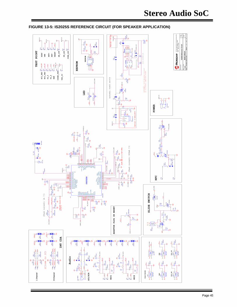
Stereo Audio SoC
Page 45
FIGURE 13-5: IS2025S REFERENCE CIRCUIT (FOR SPEAKER APPLICATION)
(Vo=(1+ R24/R16)*1.25)
C5
42
20
p/5
0V
HP
ON
2_
O
C5
22
20
p/5
0V
HP
OP
2_
O
FB
7G
SM
A2
01
20
91
2
R C
ha
nn
el
FB
8G
SM
A2
01
20
9
12
(Close to IC) H
PO
N2
HP
OP
2
MIC
2+
D1
2S
PE
0572
2 1
D1
3S
PE
0572
2 1
MIC
1+
P0_1
FWD
C6
61
5p
/50
V
VOL_UP
SW
6
SW
-TA
CT
12
34
P2_7
P0_2
U7
AC
E2
4C
64
A0
1
A1
2
A2
3
GN
D4
SD
A5
SC
L6
WP
7V
CC
8
SW
8
SW
-TA
CT
12
34
C6
81
5p
/50
V
REV
PLAY/PAUSE
C6
41
5p
/50
V
P0_3
VOL_DN
P1_2
SW
4
SW
-TA
CT
12
34
2V
8
P1_3
C6
51
5p
/50
V
R1
8N
P-0
60
3
P0_5
C3
91
u/1
6V
SW
5
SW
-TA
CT
12
34
C6
71
5p
/50
V
R1
74K
7
1 2
EEPROM
Audio
SY
S_
PW
R
MF
B
C3
80
.1u
/16
V
SW
7
SW
-TA
CT
12
34
SW
9S
W-T
AC
T
12
34
C3
00
.1u
/16
VP
3_0
HP
OP
2_
O
HP
ON
_O
P3
TS
H-3
86
5D
4 32 10
1
D2
3S
PE
0572
2 1
HP
OP
_O
D2
4S
PE
0572
2 1
CD
A_
PW
R
HP
ON
2_
O
D2
5S
PE
0572
2 1
D2
6S
PE
0572
2 1
R2
6N
P-0
80
5
R6
10
12
AIL/AIR
R6
00
12
R6
3N
P-0
60
3
AIR
R
AIL
L
R6
2N
P-0
60
3
+
C6
01
00
u/1
6V1 2
AIL
AIR
C4
21
u/1
6V
C4
01
u/1
6V
+
C6
11
00
u/1
6V
1 2
C3
31
u/1
6V
P0_0
R1
29
100K
12
SW
10
SW
-1B
IT
12
R5
2
100K
1 2
GD
S
Q14
STS
23
01
13
2
Q8
STS
23
06
31
2
SY
S_
PW
R
R5
010K
1 2
SW
3P
T-5
50
1G
12
34
VD
DIO
SLIDE SWITCH
MF
B
EEPROM
LE
D2
LE
D1
LED
SY
S_
PW
R
LE
D1
LE
D-B
12
LE
D2
LE
D-H
R1
2
C2
11
0p
/50
V
FB
6G
SM
A2
01
20
91
2
FB
5G
SM
A2
01
20
9
12
C5
02
20
p/5
0V
HP
OP
HP
OP
_O
C4
32
20
p/5
0V
HP
ON
C2
41
0p
/50
V
X1
X4
P-1
6M
HZ
41
32
L C
ha
nn
el
HP
ON
_O
U8
SM
48
39
N
S1
S2
S3
G4
D8
D7
D6
D5
L1
L1
0u
H-3
R1
6390K
12
R2
41M
12
CO
DE
C_
VO
R2
10
12
R2
2N
P-0
60
3
U2
RT
92
66
E
CE
1
EXT
2
GN
D3
LX
4
VD
D5
FB
6
D1
1N
58
22
21
INT CDA
CORE_LDO
1V
2
TP
35
1
RF
LD
O_
O
RS
T_
N
TP
28
1RF_LDO
TEST POINT
GND
ADAP
BAT-
BK_OUT
HCI_RXD
RESET
HCI_TXD
HC
I_R
XD
P2_0
P2_4
EA
N
HC
I_TX
D
TP
311
CODEC_VDD
AD
AP
_IN
TP
18
1
TP
17
1
TP
15
1
TP
20
1TP
19
1 TP
16
1
TP
21
1 TP
23
1TP
22
1T
P2
41
1V
8
TP
25
1
BA
T_
IN
TP
26
1
CO
DE
C_
VO
D1
0S
PE
0572
2 1
P2_0
BAT+
VDD_IO
P2_4
VD
DIO
TP
27
1
D1
1S
PE
0572
2 1
EAN
POWER
AD
AP
_IN
P2
DC
-JA
CK
1 2 3
2V
8
TP
321
MIC
1-
C7
10
u/1
6V
R2
1K
8/1
%
1 2
AD
AP
_IN
R2
0N
P-0
60
3
Optional if ADAP_IN>5V
EXTERNAL POWER SWITCH
C6
10
u/1
6V
C5
0.1
u/1
6V
R1
620
1 2
U1
AP
L1117-V
C
ADJ/GND1
OUT2
IN3
BA
T_
IN
R1
21
K/1
%
1 2
GD
S Q4
STS
23
01
13
2
D2
1N
40
02
21 R
15
20K
1 2
5V
TP
331
Warning! 4.5V max
MIC
_N
1
MIC
_P
1
C3
72
20
p/5
0V
R1
02K
12
C3
50
.04
7u
/25
V
C4
40
.04
7u
/25
V
MIC
1+
TP
51
MIC
_B
IAS
MIC
1-
TP
61 MIC1
R6
1K
12
C2
04
.7u
/10
VR
71K
12
TP
341
C2
24
.7u
/10
V
MIC
_N
2
MIC
_P
2
C4
52
20
p/5
0VC4
60
.04
7u
/25
V
R1
12K
12
C4
70
.04
7u
/25
V
MIC
2-
MIC
2+
TP
71 T
P8
1 MIC2
MIC
_B
IAS
R8
1K
12
C4
94
.7u
/10
VC
48
4.7
u/1
0V
R9
1K
12
R1
4
1K
1 2
C1
36
10
u/1
6V
SY
S_
PW
R
P0_4
D1
8S
PE
0572
2 1
Q7
STS
23
06
31
2
D1
9S
PE
0572
2 1
AIL
L
AIR
R
GD
SQ9
STS
23
01
13
2
R2
31M
1 2
D2
1C
DS
U4
00
B1
2
D2
0
21
D2
2C
DS
U4
00
B1
2
R2
91
20
/1%
12
R2
52
70
/1%
12
R3
01
K/1
%
1 2
R1
3N
P-0
80
5T
P2
91
MF
BT
P3
01
OPTIONAL: 4.5V Booster Circuit
If no boost, add R26 0-ohm
NFC
MIC
2-
Bo
ard
Na
me
Siz
eT
itle
Re
v
Da
te:
Sheet
of
P/N
MA
IN C
IRC
UIT
2.4
IS2025 R
efe
ren
ce
Cir
cu
it
Cu
sto
m
22
Th
urs
da
y,
Ap
ril 0
2,
20
15
XX
XX
5F
, N
o.5
, In
dustr
y E
. R
d. V
II, H
sin
chu S
cie
nce P
ark
,
Hsin
ch
u C
ity
30
07
8,
Ta
iwa
nT
EL
.
88
6-3
-57
78
38
5
(C88/C89 should close
to IC!!)
R6
91
K/1
%
1 2
AD
AP
_IN
CO
DE
C_
VO
PV
DD
2_
CD
A_
IN
2V
8
P0_1P2_4
C8
21
0u
/16
V
2V
8
P0_0
IS2025S
U6
IS2
02
5G
M
AOHPR68
AO
HP
L3
VD
DA
4
VC
OM
5
MIC
N1
8
MIC
P1
9
MIC
BIA
S10
VD
D_
CO
RE
13
VD
D_
IO17
AIR
11
RS
T_
N16
P03
42
P12
14
P13
15
P0420
HCI_TXD23HCI_RXD22
XO
_P
51
XO
_N
50
NC
49
P2756
VB
G47
RF
LD
O_
O46
PM
IC_
IN45
CL
DO
_O
44
EA
N43
UL
PC
_V
SU
S48
PVDD_CDA67
P2419
P2055
P3057
P0118
VDD_IO59
RTX53
VCC_RF52
P00
41
EP69
VD
DA
O1
AO
HP
M2
MIC
P2
7
TEST_EN24
AIL
12
HPOP_CDA66
NC
37
CODEC_VO25
LDO31_VIN26
LDO31_VO27
ADAP_IN28
BAT_IN29
SAR_VDD31
SYS_PWR32
BK_VDD33
BK_LX34
BK
_O
35
PW
R36
P35
40
LE
D1
39
LE
D2
38
NC30
P0558
P1521
HPON2_CDA62
HPOP2_CDA61
PVDD2_CDA60
HPON_CDA65
VBP_CDA64
AVDD_CDA63
MIC
N2
6
P0254
C8
11
0u
/16
V
P0_3
P0_4
FB
9G
SM
A2
01
20
9
12
FB
10
GS
MA
20
12
09
12
RF
LD
O_
O
C3
11
u/1
6V
HCI_RXD
C1
91
u/1
6V
HCI_TXD
C2
81
u/1
6V
RF
LD
O_
O
C2
91
u/1
6V
C3
21
u/1
6V
UL
PC
_V
SU
SV
BG
ADAP_IN
C8
71
u/1
6V
C7
71
0u
/16
V
1V
8S
YS
_P
WR
BA
T_
IN
CO
DE
C_
VO
C7
91
u/1
6V
(Peak current: 400mA !!)
C8
01
u/1
6V
1V
8
C8
41
u/1
6V
C8
31
u/1
6V
C7
81
u/1
6V
PV
DD
_C
DA
_IN
R6
81
K/1
%
1 2
HPON
HPON2
HPOP
C2
31
u/1
6V
C1
81
u/1
6V
HPOP2
CD
A_
PW
R
C8
81
0u
/16
V
(Peak current: 1A !!)
P0_2
C8
91
0u
/16
V
AIL
P2_7
P0_5
L3
6.8
p/5
0V
MF
B
P2_0
AIR
MIC
_N
2M
IC_
P2
C1
61
u/1
6V
P1_2
MIC
_N
1M
IC_
P1
1V
2
C2
71
u/1
6V
C8
61
u/1
6V
MIC
_B
IAS
LE
D1
UL
PC
_V
SU
S
VB
G
LE
D2
C2
61
u/1
6V
C3
41
u/1
6V
C2
51
u/1
6V
+
C1
18
10
0u
/16
V
1 2
1V
8
SY
S_
PW
R2V
8
P1_3
SY
S_
PW
R
+
C1
17
10
0u
/16
V
1 2
RS
T_
N
1V
2
C4
11
u/1
6V
C3
61
u/1
6V
P3_0 P3_0
TP
9
RF
-TP
1
AN
T1
AN
T-M
P8
1
(1uF X5R or 4.7uF Y5V)
C4
NP
-04
02
L2
1nH
C3
NP
-04
02
L10
L1
0u
H-2
ADAPTOR PLUG IN RESET
C7
01
u/1
6V
AD
AP
_IN
RS
T_
N
Q3
MM
BT3
90
4
32
1
R2
82K
1 2
Stereo Audio SoC
Page 46
14.0 PACKAGE INFORMATION 14.1 CHIP IDENTIFICATION SYSTEM PART NO. X -Y (Chip Name) (Package Type) (Version) Chip name: IS2020 IS2021 IS2023 IS2025 Package Type: S = QFN (Saw Type) Package Version: e.g. “-203” is means the chip version is 203.
Examples: a) IS2020S-002: 002 version ROM code IS2020 chip in QFN type package.
b) IS2025S-203: 203 version ROM code IS2025 chip in QFN type package.
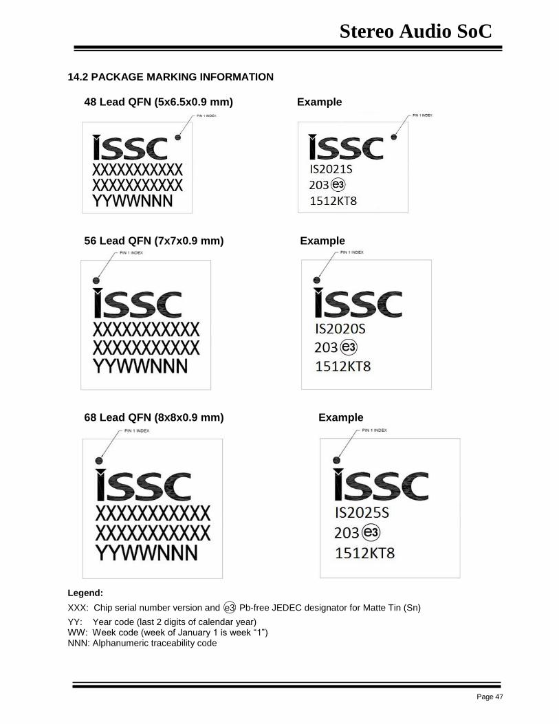
Stereo Audio SoC
Page 47
14.2 PACKAGE MARKING INFORMATION
48 Lead QFN (5x6.5x0.9 mm) Example
56 Lead QFN (7x7x0.9 mm) Example
68 Lead QFN (8x8x0.9 mm) Example
Legend:
XXX: Chip serial number version and ○e3 Pb-free JEDEC designator for Matte Tin (Sn)
YY: Year code (last 2 digits of calendar year) WW: Week code (week of January 1 is week “1”) NNN: Alphanumeric traceability code
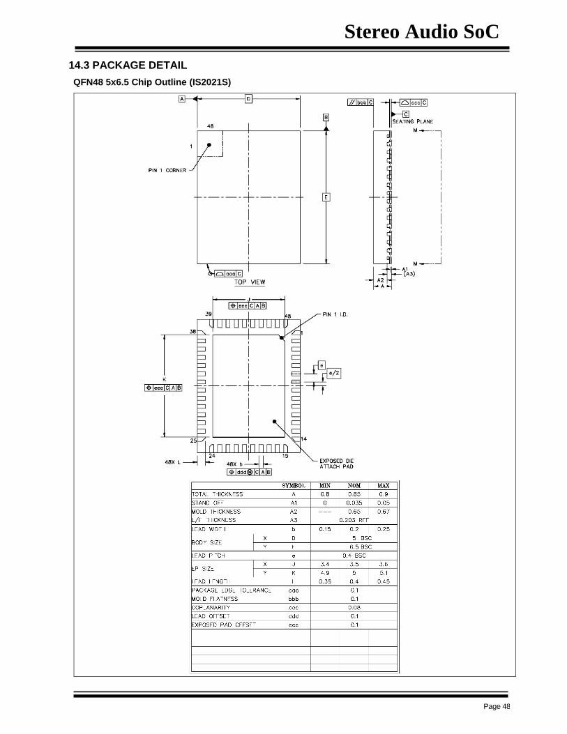
Stereo Audio SoC
Page 48
14.3 PACKAGE DETAIL
QFN48 5x6.5 Chip Outline (IS2021S)
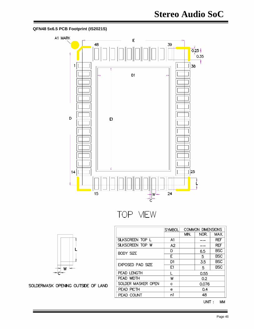
Stereo Audio SoC
Page 49
QFN48 5x6.5 PCB Footprint (IS2021S)
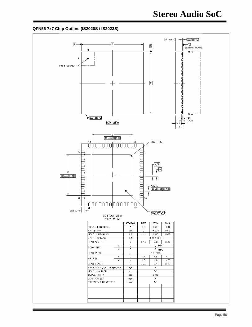
Stereo Audio SoC
Page 50
QFN56 7x7 Chip Outline (IS2020S / IS2023S)
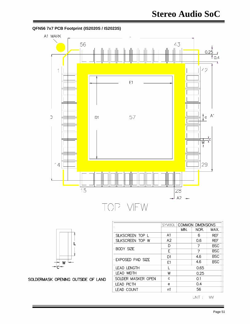
Stereo Audio SoC
Page 51
QFN56 7x7 PCB Footprint (IS2020S / IS2023S)

Stereo Audio SoC
Page 52
QFN68 8x8 Chip Outline (IS2025S)
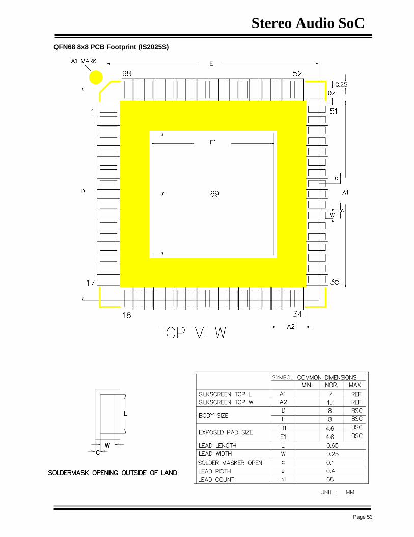
Stereo Audio SoC
Page 53
QFN68 8x8 PCB Footprint (IS2025S)
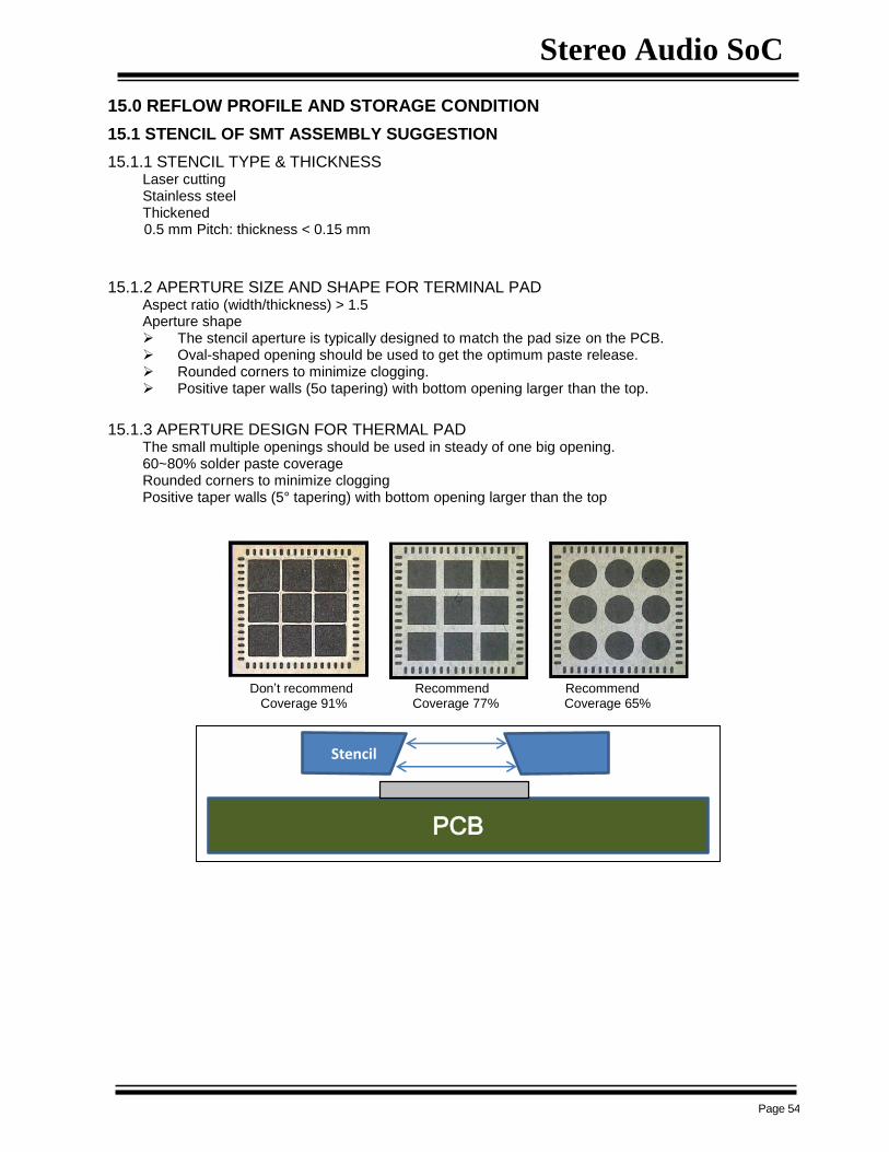
Stereo Audio SoC
Page 54
15.0 REFLOW PROFILE AND STORAGE CONDITION
15.1 STENCIL OF SMT ASSEMBLY SUGGESTION
15.1.1 STENCIL TYPE & THICKNESS Laser cutting Stainless steel Thickened 0.5 mm Pitch: thickness < 0.15 mm
15.1.2 APERTURE SIZE AND SHAPE FOR TERMINAL PAD
Aspect ratio (width/thickness) > 1.5 Aperture shape The stencil aperture is typically designed to match the pad size on the PCB. Oval-shaped opening should be used to get the optimum paste release. Rounded corners to minimize clogging. Positive taper walls (5o tapering) with bottom opening larger than the top.
15.1.3 APERTURE DESIGN FOR THERMAL PAD
The small multiple openings should be used in steady of one big opening. 60~80% solder paste coverage Rounded corners to minimize clogging Positive taper walls (5° tapering) with bottom opening larger than the top
Don’t recommend Recommend Recommend Coverage 91% Coverage 77% Coverage 65%
PCB
Stencil
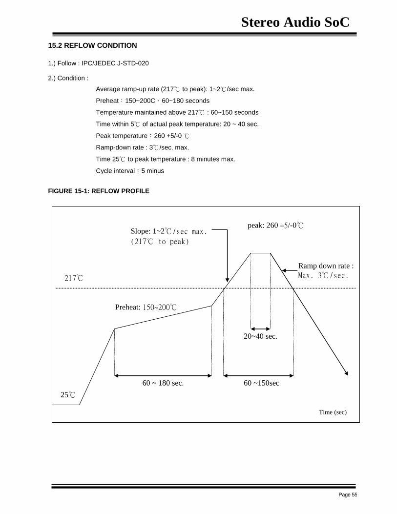
Stereo Audio SoC
Page 55
15.2 REFLOW CONDITION
1.) Follow : IPC/JEDEC J-STD-020 2.) Condition :
Average ramp-up rate (217℃ to peak): 1~2℃/sec max.
Preheat:150~200C、60~180 seconds
Temperature maintained above 217℃ : 60~150 seconds
Time within 5℃ of actual peak temperature: 20 ~ 40 sec.
Peak temperature:260 +5/-0 ℃
Ramp-down rate : 3℃/sec. max.
Time 25℃ to peak temperature : 8 minutes max.
Cycle interval:5 minus
FIGURE 15-1: REFLOW PROFILE
Slope: 1~2℃/sec max.
(217℃ to peak)
Ramp down rate :
Max. 3℃/sec.
Preheat: 150~200℃
25℃
217℃
Time (sec)
peak: 260 +5/-0℃
60 ~ 180 sec. 60 ~150sec
20~40 sec.
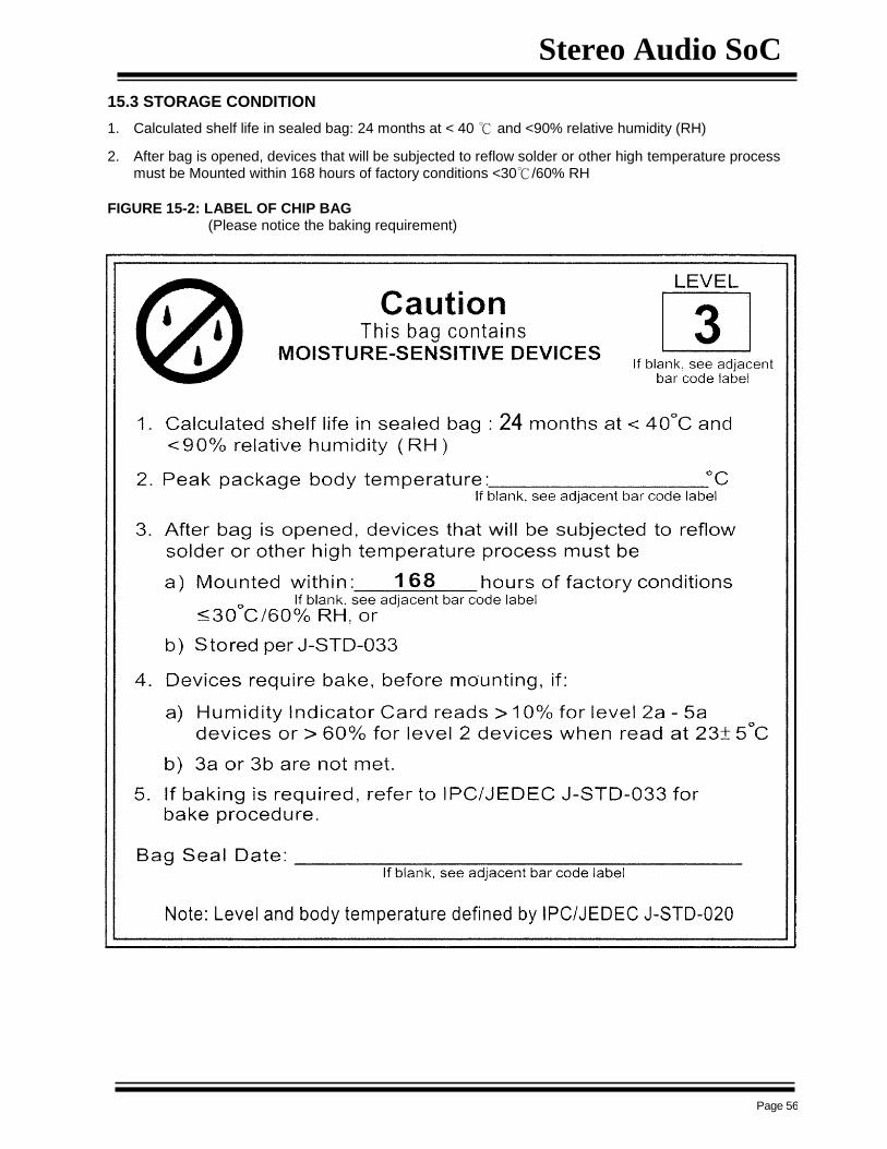
Stereo Audio SoC
Page 56
15.3 STORAGE CONDITION
1. Calculated shelf life in sealed bag: 24 months at < 40 ℃ and <90% relative humidity (RH)
2. After bag is opened, devices that will be subjected to reflow solder or other high temperature process must be Mounted within 168 hours of factory conditions <30℃/60% RH
FIGURE 15-2: LABEL OF CHIP BAG (Please notice the baking requirement)


![RN4020 Bluetooth Low Energy Module Data Sheetww1.microchip.com/downloads/jp/DeviceDoc/50002279A_JP.pdf10 CONNECTION LED PIO[1] SCK 既定値の状態は出力: アクティブHIGH](https://img.pdfslide.net/doc/110x75/5e5d7dbf2d4e3a7a0165f6a9/rn4020-bluetooth-low-energy-module-data-10-connection-led-pio1-sck-c.jpg)