Embed Size (px)
Citation preview

r
Serial Number
Filing Date
Inventor
09/157.002
18 September 1998
Harry F. Francis Thomas F. Cocke. IV Gary S. Calvert. II Roland H. Mattoon Timothy Y. Gorder Neil E. Moody Gair D. Brown
NOTICE
The above identified patent application is available for licensing. Requests for information should be addressed to:
OFFICE OF NAVAL RESEARCH DEPARTMENT OF THE NAVY CODE OOCC ARLINGTON VA 22217-5660
/
SKQ^^Erril-r^^^ s
ro
r**>

f
J
25
MC W 93
MULTI-INTERFACE POINT-TO-POINT SWITCHING SYSTEM (MIPPSS)
5 WITH RAPID FAULT RECOVERY CAPABILITY
BACKGROUND OF THE INVENTION
1. Field of the Invention
10 The present invention relates generally to switching systems. More specifically, the present
invention relates to a switching system which provides the ability to interconnect a large number of
electronic components in a manner which allows the components to function as if they were
physically wired together using virtually any type of data transfer protocol while exhibiting low
latency (achieving a total data transfer delay close to the that which would have been achieved in a
15 direct-wired configuration), timing consistency (achieving a latency which is deterministic and
predictable), and high signal fidelity (not adding to, deleting from, or altering the signal in any way).
2. Glossary
Before beginning a discussion of either the related art or the preferred embodiments according to the
20 present invention, it should be mentioned that the inventors have opted to employ the following
terms throughout the specification. A glossary of these terms are set out immediately below.
Blocking - Blocking refers to a condition wherein a connection is refused even though there are free
input and output channels.
Contention - refers to an attempt to connect an input port to an output port which is already in use.
Data Transfer Protocol Insensitive - Data transfer protocol insensitive functional behavior refers
to the ability to of the switching system to handle virtually any type of data transfer protocol, i.e.,

any device can be connected to any other device that uses that same data transfer protocol, without
adding to, deleting from, altering, or responding to the transfer protocol in any way. From the
discussion immediately above, it will be appreciated that neither the origin nor the destination of any
signal is determined by analyzing the associated header or the data content of the signal; switching
5 is completely content-independent or message-independent.
Deliver - Deliver, as used hereinafter, is employed to connote that any specification-compliant
signal received is switched and "delivered" as a corresponding specification-compliant output signal.
"Delivered" is understood to be broad enough to encompass the general process wherein the input
10 signal, once recognized as a valid signal, is converted into one or more other signal formats as it is
handled within the switch, so long as the final output signal "delivered" by the MIPPSS is
specification-compliant in its original format.
Distributed System - Distributed system refers to the switching system design wherein each
15 switching unit has the capability of servicing multiple locations, and no single location must house
the entire switch. It will be appreciated that this reduces need for costly modifications or additions
to facilities to accommodate switching equipment.
Hot-Swapping - Hot- swapping capability refers to the ability to perform on-line replacement of
20 line-replaceable units, i.e., the switching system remains operable overall while discrete, inoperable
elements are replaced.
Low Latency- Low latency refers to the ability of the switching system to achieve a total data
transfer delay close to the that which would have been achieved in a direct-wired configuration.
25
Multi-Interface - Multi-Interface functional behavior refers to the ability to handle virtually any
type of data transfer protocol, i.e., any device can be connected to any other device that uses that
same data transfer protocol.
-2-
NTDS - Naval Tactical Data System (NTDS) refers to the Navy's specific implementation of the
Military Standard Document entitled "Input/Output Interfaces, Standard Digital Data, Navy
Systems," commonly referred to as MIL-STD-1397 (NAVY). The standard describes interface
classifications (Types) and categories of NTDS interfaces, the latter being parallel interfaces, serial
5 interfaces, and other interfaces. For specific information of each NTDS signal type, refer to MTT,-
STD-1397 (NAVY), the latest version of which, MIL-STD-1397C, is available from the Naval
Publications and Forms Center, Philadelphia, PA, or at http://www.dodssp.daps.mil. MEL-STD-
1397 is incorporated herein by reference.
10 Point-to-Multipoint - Point-to-multipoint functional behavior refers to the ability by which a single
data generating device (root node) communicates with a plurality of data receiving devices (leaf
nodes). In nodal notation, traffic on the switching system is generated by the root node and received
by all of the leaf nodes. Moreover, the switching system does not reserve bandwidth for traffic from
any of the leaf nodes toward the root node and the leaf nodes cannot communicate with one another
15 through the point-to-multipoint connection. A switching system capable of point-to-multipoint
connections is said to include a broadcast capability.
Point-to-Point - Point-to-point functional behavior generally refers to the ability to connect devices
which are required to communicate with one another on a one-to-one basis.
20
Signal Fidelity - Signal fidelity refers to the ability to replicate the input signal at the output port.
High signal fidelity denotes that the signal is delivered without adding to, deleting from, or altering
the signal in any way.
25 Switch Fabric - The components with a switching system that provides paths for the connections.
In the discussion which follows, two distinct types of switch fabrics will be considered. The first
type is multi-layer switch fabric, where the switch fabric is arranged in layers, i.e., discrete switch
enclosures, according to the signal format the individual layers are designed to receive and/or
-3-
output. The second type is mixed-layer switch fabric, wherein multiple signal formats are received
and/or output by a single switch layer, e.g., a single switch enclosure.
Timing Consistency -Timing consistency refers to the ability of the switching system to achieve
5 a latency which is deterministic and predictable. See low latency.
Transparency - Transparent functional behavior refers to the ability to deliver a signal without
interaction with the interface protocol corresponding to that signal. Thus, an interface-compliant
input signal bit arriving at an input terminal is output as an interface-compliant signal bit,
10 irrespective of whether the bit is a control bit or a data bit. This characteristic is critical when the
switch serves to connect objects which are themselves under test, allowing research and testing
without introducing additional possible sources of errors due to switching.
3. Brief Discussion of Related Art
15 The primary utility of MPPSS is in transparently switching signals between and among
components which may not have been originally designed to be switched. The signals can be of
virtually any data type (communications, images, sensor data, accounting records) and can be used
for any scientific, commercial, or military purpose. See Fig. 1.
20 The discussion immediately below provides a review of basic digital communications. In
addition, the discussion outlines the need for switching, current methods and apparatus used to
perform switching, and the principal limitations and disadvantages of these methods. Several
solutions to the overall switching problem solved by MIPPSS are also discussed.
25 Digital equipment communicates by sending digital signals, which are composed of binary
digits, or bits. Each bit represents either a 1 (one) or a 0 (zero). Fig. 2 shows a representative bit
expressed as a deflection from a baseline over a period of time. By convention, most upward
deflections are signed positive. The presence of a 1 or a 0 is interpreted according to an agreed-upon
encoding technique, as described in greater detail below, but it should be noted here that the presence
-4-

10
of a 1 or a 0 may be denoted by positive or negative deflections, positive or negative transitions, or
simply by the presence or absence of a transition. Digital signaling is generally superior to analog
information transfer because it is capable of very accurate transmission over great distances.
It will be appreciated that the bit is signaled in a digital circuit by varying voltages. The most
common digital logic, transistor-transistor logic (TTL), uses +0.5 volts nominal for a low signal and
+5 volts nominal for a high signal. A faster logic, emitter-coupled logic (ECL), uses -1.75 volts
nominal for low and -0.9 volts nominal for high. Positive Emitter-Coupled Logic (PECL) uses
nominal +3.0 volts for low and +4.0 volts for high.
It should be mentioned here that when the signal needs to be transmitted over a distance, a
device called a driver receives the digital logic input, adds energy, and produces a current sufficient
to transmit the signal. However, regardless of the propagation distance, it is important to note that
the shape of the signal bit may vary in terms of its overall amplitude, duration, and direction of
15 deflection (polarity). The allowable limits on the exact shape of signal bits are precisely defined in
interface specifications. This precise definition helps to ensure that noise is not interpreted as data.
The transmission of digital data from one machine to another must ensure that the data is
received unambiguously and accurately. Various encoding techniques are used depending on the
20 requirements of the interface (distance, timing, environment, etc.). Some common forms of
encoding are illustrated in Fig. 3 and include:
a. Return to Zero (RZ). A simple approach to digital communication might prescribe
an upward deflection to signal the presence of a 1 bit, and the absence of this
25 deflection to signal a 0 bit (Figure 3(a)). In this case it takes an entire time interval,
or bit period (shown as the horizontal distance between the vertical grid lines) to
signal a 0, not simply the return to baseline which occurs following each 1 bit. This
interpretation requires some type of timing signal to coordinate bit periods between
different equipment.
-5-

b. Non-Return-to-Zero (NRZ). In Figure 3(b), a continuous signal might transmit at
either one level or another throughout each time interval, eliminating the need for a
return to baseline within each interval. Again, some form of time synchronization
is required.
5
c. Manchester. An improvement to these signaling schemes uses just a down-shift to
signal a 1 and an up-shift to signal a 0 (Figure 3(c)). This shift must occur in the
middle of the bit period for the signal to be valid.
10 d. Non-Return-to-Zero, Inverted (NRZI). A further refinement defines that simply a
transition across the time interval boundary indicates a 0 and the lack of a similar
transition indicates a 1 (Figure 3(d)).
Each of these encoding methods has distinct advantages and disadvantages in aspects such as overall
15 signaling speed, average power consumed, error rates, and the need for a separate clock.
It should be mentioned that encoding is performed to enable data transfer and not to provide
secrecy. It will also be understood that distinct strings of bits may be encoded to represent letters
and words. Once again, the goal of these codes is not secrecy but the establishment of distinct and
20 unambiguous meanings for various bit patterns. Two of the more common encoding schemes are
as follows:
a. ASCII. One common encoding scheme is ASCII, the American Standard Code for
Information Interchange, published by the American National Standards Institute.
25 ASCII uses a seven-bit string to signal different English alphanumeric characters.
The use of seven bits limits the character set to 27 = 128 different characters.
-6-

EBCDIC. IBM increased the number of possible characters to 256 by using an eight-
bit coding system known as the Extended Binary Coded Decimal Interchange Code
(EBCDIC). Representative values of these codes are shown in Table 1.
10
Table 1: Common Binary Codes
Character ASCII EBCDIC
A 100 0001 1100 0001
Z 101 1010 1110 1001
5 0110101 11110101
etc. etc. etc.
Other data processing systems use different binary coding systems with different numbers of bits,
sometimes adding extra bits for error detection/correction.
15 It should be noted that digital signals may be transmitted between two communicating
components via single- or multiple-conductor electrical (or fiber optic) cables. In order to
communicate, sending and receiving components must agree upon the format of the signals they
exchange. Common signal formats include serial (one bit at a time over a single conductor) and
parallel (several bits at a time over multiple-conductor cables). See Fig. 4. It will be appreciated
20 that fiber optic transmission usually involves a serial-format transmission over a fiber optic cable.
25
Although all signals are bound by the physical limit on transmission speed in any particular
medium (and none can exceed the speed of light), signal formats may differ in how frequently they
inject or extract data on the communication channel, as defined in their interface specifications.
Numerous private, public, and international interface standards exist. Interface standards also
include timing considerations and descriptions of associated control signals, such as "ready to send,"
"ready to receive," etc.
-7-

Other standards allow for more complex manipulations of data. It is possible (and commonly
practiced) to inject multiple signals on a single communication channel by subdividing time intervals
or frequency bands on the communication channel; this technique is generally known as
multiplexing. It should also be mentioned that another increasingly common signal manipulation
5 is data compression and decompression according to specific algorithms.
Most modern technical, commercial, and scientific activities simultaneously use a wide
variety of digital data sending and receiving devices. These devices include not only computers, but
an increasing number of peripherals which now generate digital data such as medical imaging
10 equipment, radars, and voice communications systems. The wide variety of these systems is further
increased by the fact that different systems are bought over time, each differing slightly from
previous models. Interoperability is highly desirable in order to take advantage of still-useful
equipment (collectively known as legacy systems).
15 The physical and electrical arrangement of components within any facility usually is not
permanently fixed. Components are taken off-line for maintenance or repair, new components are
added, and old components are removed. Activity missions frequently change, and data processing
resources are re-aligned according to the task at hand, sometimes on an hourly basis. For example,
a large financial institution may choose to re-align resources to perform end-of-month invoice
20 processing. In contrast, a military facility may choose to disconnect external communication devices
in order to process classified data. It is usually cost prohibitive to purchase multiple equipment
suites with overlapping capabilities to perform different missions. Realigning resources is more cost
effective.
25 In order to realign components in response to mission changes, i.e., changes in facility usage,
the activity may choose to unplug components and re-route the associated cables. Dozens of devices
with dozens of input-output (I/O) channels each implies hundreds or potentially thousands of cables.
These cables are frequently in crowded under-floor spaces or cable trays, and may need to be cut,
spliced, and/or re-manufactured to fit new routes.
-8-

Switching is the most cost-effective method for realigning resources. A multiple-interface
switch allows an activity to interconnect a wide variety of components while avoiding the need to
manually re-route cables. In the discussion which follows, it should be assumed that the overall
switching system design requirement specifies point-to-point switching unless the discussion states
5 otherwise.
The most common type of a switch is a mechanical switch. Original point-to-point electrical
signal switching equipment included simple multi-pole mechanical switches used for early
telegraphy, and patch cables used by operators on early telephone systems. Fig. 5 illustrates a simple
10 single-pole, dual-throw (SPDT) switch. Variants of mechanical signal switches still exist in many
modern buildings. For example, although Fig. 5 shows a single communication line on the input
side, multi-conductor (i.e., parallel) switches are common. Mechanical switches provide a rugged,
relatively inexpensive point-to-point switch path. Mechanical switches are useful where rapid or
frequent equipment realignments are not required, or for distributing analog (non-digital) signals
15 such as radar and/or video signals. Because these switches involve mechanical moving parts and
contacts, they require periodic maintenance, they are subject to wear and tear, and they are
susceptible to eventual failure. Mechanical switches can be remotely controlled (opened and closed)
using electrical remote control circuits. In general, mechanical switches are useful in small-scale
applications with a limited number of destinations and where limited growth is expected.
20
It will be appreciated that additional destination poles can be added. Such switches are
generally referred to as 1 x n or multi-pole switches (where n represents the number of available
destinations). They include T-Bar Corporation's T-Bar switches and Purvis Corporation's MultiPort
switches. These are depicted schematically in Fig. 6. Notice that it is possible to gang these
25 switches to achieve an increased value of n; Fig. 6 shows an effective 1 x 3 switch achieved by
splitting one of the outputs of the first 1x2 switch. Multi-pole switches up to 1 x 8 are commonly
available.

Another common switch type is a crosspoint switch. It should be mentioned that early
crosspoint switches were implemented via a relay design by the Bell Telephone Company for their
telephone switching centers. These switches have mostly been replaced by solid state crosspoint
switches. Moreover, an electric path between multiple inputs and multiple outputs can be effected
5 using solid-state technology known as crosspoint switching. At the highest level, these electronic
switches appear as nxm switches, as shown in Fig. 7. These switches may also be commonly
referred to as matrix switches. Examples include the Navy's High-Speed Digital Switch
(HSDS)(AN/USQ-62(V)) and Low-Level Serial (LLS) Switch (AN/FSQ-157(V)). HSDS is
implemented in several Navy sites in either 256 x 256 or 1024 x 1024 configurations. Integrated
10 crosspoint switch circuit elements containing 32 x 32 switches on a single chip are common.
Symmetry is not required; a 64 x 33 crosspoint switch provides 64 inputs and only 33 possible
outputs.
Referring to Fig. 7, it should be noted that although the lines appear to lay across each other
15 and therefore electrically connect, the connection is actually controlled by an AND gate which
provides a method for external control. See Fig. 8. An AND Gate is a logical device whose output
is 1 only when both inputs are 1. Lacking a 1 signal on the control line, the AND gate will not
produce an output and the crosspoint is not connected. It will be appreciated that reconfigurable
crosspoint switches require less switch allocation planning than mechanical switches and consume
20 fewer resources per switched channel than mechanical switches, especially when mechanical
switches must be ganged.
A variant of the conventional crosspoint switch is the minimized crosspoint switch. The
principal problem with crosspoint switches is that the number of required crosspoints grows as the
25 square of the number of input lines. In Fig. 7 above, the simple crosspoint switch for eight input
channels and eight output channels requires 8 x 8, or 64 crosspoints. A simple 100-channel switch
requires 10,000 crosspoints, and each crosspoint requires a separate control line. This number can
be dramatically reduced by eliminating self-connections and assuming bi-directional (full duplex)
communications. Fig. 9 illustrates the eliminated crosspoints within the shaded area achievable
-10-

using a minimized crosspoint switch. The general equation for the number of required crosspoints
in a minimized crosspoint switch with n inputs is:
Minimum number of crosspoints = n (n -1)/2 (1)
5
The number of physical switches needed to provide, for example, sixteen signal paths can
also be minimized by the use of multi-stage switching. Stated another way, crossbar switch size and
complexity can be reduced by using intermediate stages. Fig. 10 shows a multi-stage switch (also
known as a space division switch). In the exemplary multi-stage switch illustrated in Fig. 10, a
10 virtual JVxiV(16xl6) switch has been created using four 4x2 input crossbars, two 4x4
intermediate stage crossbars, and four 2x4 output crossbars. Instead of having the 16x16 = 256
crosspoints of a simple crosspoint switch, or the n(n-\)l2 =120 crosspoints of a minimized
crosspoint switch, this switch uses only 96 crosspoints. The general equation for the number of
crosspoints is:
15
Number of crosspoints = 2kN + k(N/n)2 (2)
It should be mentioned here that although some reduction in complexity is achieved by
staging, blocking is possible when there is contention for one of the intermediate stages. As
20 mentioned above, blocking is a condition where a connection is refused because the switch assets
are already being used to connect other devices. In Fig. 11, all eight available intermediate stage
channels are used (shown by heavy lines with arrows), indicating that additional connections cannot
be made, even though there are free input and output channels. It will be appreciated from equation
(2) that adding additional intermediate stages will ease the bottleneck; when the number of
25 intermediate stages (k) equals 2n -1, the switch will not block, as noted by Clos in an article entitled
"A Study of Non-Blocking Switching Networks," which article appeared in Bell System Technical
Journal, Volume 32, pp. 406-424, March 1953. It will also be appreciated that the decision whether
or not to add intermediate stages is usually based on total cost, complexity, physical space, and
performance requirements.
-11-

Referring now to Figs. 12A and 12B, the concept behind a conventional trunk switch will
now be discussed. Referring to Fig. 12A, the illustrated trunk cable provides a heavily loaded
system a degree of flexibility by directly connecting ports on two different switches. It should be
noted that trunk cables are used when the size of a switch becomes inadequate for user requirements
5 or there are not enough switching assets close enough to the equipment channels which need to be
switched. The use of trunk cables consumes available switching ports in static, unswitchable
applications. Fig. 12B illustrates the use of a trunk switch. This type of switch is used to allow a
path to equipment that is not directly accessible from another switch. Like trunk cables, the use of
trunk switches is cost-prohibitive. Again, this type of switching arrangement usually is the result
10 " of expanding switching requirements beyond their intended maximum requirements.
Packet switching is a widely used alternative to point-to-point switching. Although
communication via local and wide-area computer networks (LANs and WANs) has grown in
popularity in the past several years, such networks do not offer a complete solution to the point-to-
15 point switching problem. Most networks handle long-distance communications by using a process
of packet switching in which larger messages are broken up into transmittable portions (packets),
several layers of header data are added, and the message (data) proceeds through a series of
intermediate destinations until its final destination is reached. Fig. 13 shows a typical packet
switching network. Points A and M could represent opposite ends of an office (LAN) or offices in
20 separate cities hundreds of miles apart (WAN).
It will be appreciated that data packets may be buffered (stored) until intermediate channels
are available. Depending on the specific network technology selected, packets may follow different
paths to the same destination, such as those shown by the heavier solid lines and the heavier dashed
25 lines connecting A and M. This means that the packets may arrive out of order at the destination,
or may simply be lost in transmission. The processor at the destination must collect and inventory
packets, remove header data, and then re-assemble and verify the message. In addition, if the
network is used by multiple participants, some form of contention arbitration scheme is required.
-12-

10
Arbitration implies some form of selection, momentary storage, and delayed transmission of a
packet.
Current switching technology has several limitations and disadvantages including:
a. Limited Capacity. Mechanical switches are not adequate for the sheer volume of
switched interfaces in modern facilities; the amount of time and labor required to
manually re-set a large number of switches is usually prohibitive and error-prone.
Mechanical switches also require regular maintenance and are prone to failure;
b. Limited Interface Types. Crosspoint switches usually handle only one interface type
(e.g., parallel or serial);
c. Complexity. While modern integrated circuit technology can accommodate
15 thousands of crosspoints, connecting thousands of data and control conductors to a
single chip is unreasonably complex and expensive as the number of data and control
channels increases. Multi-stage switches allowthe use of smaller but more numerous
crosspoint switches, but at the cost of possible blocking. Adding sufficient
intermediate stages to forestall blocking re-introduces design complexity;
20
d. Performance Inconsistency. Packet switching over LANs and WANs, while very
useful for many purposes, is fundamentally not deterministic in large applications
where dynamic traffic loads cause variations in routing, timing, and (in some
architectures) possible losses of packets. This method of communication is therefore
25 not useful in data transfer applications where the signal route and elapsed time must
be consistent and predictable (such as when the computer system itself is under test);
e. Unmanageable Physical Components. Most current switching designs are not
distributable. The physical arrangement of devices is bounded by both the speed of
-13-

electrical signals and the ability to humanly manage the installation. Equipment
layout considerations are further complicated by distance limitations imposed by line
losses associated with any purely passive device. If the switch's physical resources
are not distributable, they may require a large amount of contiguous space in already
crowded and expensive facilities; and
10
f. Procurement Challenges. A single switch of a given capacity, even if available and
technically suitable, would most likely be difficult to acquire since the total switching
needs of any facility are difficult to predict. A scalable design allows users to
purchase adequate resources for current needs while leaving the option open for
future system expansion in response to future system needs.
15
Alternative designs which use combinations of the current technology are also presently
available. Several alternative designs are described immediately below. These descriptions also
note the problem(s) associated with each alternative design. Table 2 below summarizes the
disadvantages of the alternative designs.
20
Table II - Disadvantages of Alternative Designs
Alternative Design Disadvantages
#1: Large Matrix Switch Separate converters required Cable congestion Cable length limitations Physical size
#2: Network Approach Timing inconsistencies High latency Possible lost/out-of-order packets
#3: Mixed System Very difficult logistics Inefficiencies in trunking Cable congestion
-14-

Alternative Design No. 1 is simply a large matrix switch. See Fig. 14 A. If both electrical
and fiber optic signals are to be passed through the same switch, then some form of converters are
required. The disadvantages of this design include cable congestion in and around the matrix switch,
cable length limitations, and the physical size of the switch. Required converters would introduce
5 a relatively high latency in electrical parallel and fiber optic paths.
Alternative Design No. 2 is a network approach, as illustrated in Fig. 14B. Once again,
numerous conversions must be performed in order to access the network. The specific disadvantages
of this design include timing inconsistencies, high latency (due to packetization, channel arbitration,
10 and other network management overhead), and possible lost or out-of-order packets. A leading high-
speed network transfer protocol, ATM (Asynchronous Transfer Mode), for example, does not
guarantee packet delivery.
Alternative Design No. 3 calls for a mixed system of different types of switching, i.e., a
15 multi-layer switch fabric. This is frequently the "real world" system which has evolved in many
facilities. As shown in Fig. 14C, this type of system uses several different switches, often of
different types, to route signals between and among other serviced equipment and other switches.
The switches shown may be matrix switches, mechanical switches, or fiber optic switches, each with
its own conversion requirements. The major disadvantages of this system include very difficult
20 logistics, making parts support and maintenance very costly and inefficient; inefficiencies in trunking
(using up switch ports), and frequently the same cable congestion problems found in large matrix
switches. In addition, converters would be required on all of the serial or parallel ports to make all
signal interface formats the same upon entering the switch.
25 What is needed is a switching system capable of interconnecting a large number of electronic
components in a manner which allows the components to function as if they were physically hard
wired to one another. Preferably, the functional behavior of the switching system would be such that
one device that uses virtually any type of data transfer protocol can be connected to any other device
that uses that same data transfer protocol. Advantageously, the functional behavior of the switching
-15-

system would be such that the switching system would exhibit low latency (achieving a total data
transfer delay close to the latency associated with a direct-wired configuration), timing consistency
(achieving a latency which is deterministic and predictable), and high signal fidelity (not adding to,
deleting from, or altering the signal in any way). What is also needed is a switching system capable
5 of handling multiple signal types up to 10 kilometers (km) apart under the verified control of a single
controller.
SUMMARY OF THE INVENTION
Based on the above and foregoing, it can be appreciated that there presently exists a need in
10 the art for a switching system which overcomes the above-described deficiencies. The present
invention was motivated by a desire to overcome the drawbacks and shortcomings of the presently
available technology, and thereby fulfill this need in the art.
Advantageously, the Multi-Interface Point-to-Point Switching System (MffPSS) according
15 to the present invention provides the ability to interconnect a large number of electronic components
in a manner which allows the components to function as if they were physically wired, i.e., hard
wired, together. It should be noted that while each of these qualities may already exist separately
in other switching components, MEPPSS is the first switching system which advantageously
combines all of these features and attendant advantages within a single design.
20
An object according to the present invention is to provide a switching system which correctly
recognizes a plurality of different signal shapes while disregarding system noise.
Another object according to the present invention is to provide a switching system which
25 accommodates a plurality of different digital encoding techniques.
Still another object according to the present invention is to provide a switching system
designed to handle multiple interface types while operating at a bit, and not a word or character,
level. Stated another way, the switching system according to the present invention makes no attempt
■16-

to interpret a bit string; it simply passes the bit string along without modification. Thus, the
switching system disregards different data formats or signal manipulations and simply transfers the
signal to the appropriate destination as it is presented.
5 A still further object according to the present invention is to provide a switching system
operating under an automated controller and using pre-established configuration definitions so as
to permit re-alignment of the switching system in seconds rather than hours or days.
Yet another object according to the present invention is to a provide a switching system
10 which avoids the problems of network or packet-switched systems including the processing delays,
overhead, and timing inconsistencies associated with network protocols, while providing the high-
fidelity, point-to-point data transfer required in many scientific and technical applications.
Another object according to the present invention is to provide a switching system which
15 rapidly handles a large number of interface protocols, retains low latency which is deterministic and
predictable, and maintains high signal fidelity, all within a manageable and budgetable envelope.
An object according to the present invention is to provide a switching system exhibiting
multi-interface functional behavior. It should be noted that multi-interface functional behavior
20 connotes that a device that uses virtually any type of data transfer protocol can be connected to any
other device that uses that same data transfer protocol. Advantageously, MIPPSS is capable of
simultaneously handling various parallel and serial signal formats, at different data rates and
different voltage levels, and fiber optic signals. These signals can be of virtually any data type, i.e.,
communications, images, sensor data, accounting records, and can be used for any scientific,
25 commercial, or military purpose. MIPPSS offers the advantage of using a single system operating
under a single controller to provide all switching services for a given facility.
Another object according to the present invention is to provide a switching system exhibiting
a data transfer speed approximating that of dedicated copper wire, i.e., a data transfer speed close
■17-

to the speed which would have been achieved in a direct-wired configuration wherein the total point-
to-point delays appear as a fixed length of cable. Stated another way, the switching system
according to the present invention overcomes the disadvantages, i.e., inconsistent routing,
inconsistent timing, and packet delays (or losses) associated with the overhead of operating a packet-
5 switching network.
Still another object according to the present invention is to provide a switching system
exhibiting timing consistency, i.e., a data transfer speed which is deterministic and predictable.
10 A further object according to the present invention is to provide a switching system
exhibiting high signal fidelity, i.e., a switching system which does not add to, delete from, or alter
the signal in any way, and/or transparency.
A still further object according to the present invention is to provide a switching system
15 having a distributed design, i.e., each switching unit has the capability of servicing multiple locations
and, thus, no single location houses the entire switch system.
A related object according to the present invention is to provide a switching system designed
and implemented with standardized units or dimensions to thereby promote flexible use.
20
A still further object according to the present invention is to provide a switching system
wherein the switch size can be increased or decreased in increments of two I/O pairs from a
minimum size of two I/O pairs up to a maximum of TV I/O pairs of any interface type, where N is a
positive integer. Preferably, N is equal to 4096 in the exemplary embodiment discussed below,
25 although N may be much greater than 4096.
Another object according to the present invention is to provide a switching system which
automatically locates the quickest (lowest latency) available signaling path and establishes a point
to point connection using that path.
-18-

10
15
An object according to the present invention is to provide a switching system exhibiting a
high message throughput in addition to a high transfer speed of raw data. Preferably, the switching
system achieves ahigh message throughput by taking advantage of local switching between adjacent
components. A closely related object according to the present invention is to provide a switching
system wherein once a transmission path has been established, that transmission path cannot be used
to transmit any other signal for the duration of the connection. It should be mentioned that the
switching system according to the present invention, by combining the characteristic of local
switching and a dedicated path usage, i.e., a path once set stays set, permits messages to be
transmitted efficiently without address interpretation required in other switching architectures.
A further object according to the present invention is to provide a switching system wherein
each connection is verifiable. In particular, a given switch action advantageously can be validated
by sending an electric pulse from the input port to the output port; if the signal is received at the
intended output, the connection is valid.
Another object according to the present invention is to provide a switching system exhibiting
path selectability, whereby any given path through the switch may be selected via software
commands. Preferably, the switching system automatically chooses the switchable path that exhibits
the lowest timing delay. As mentioned above, this path, once made, remains fixed until actively
20 released. Advantageously, there are alternate paths that are software selectable.
Yet another object according to the present invention is to provide a switching system
exhibiting a non-blocking characteristic, i.e., any signal input can be switched to any signal output.
Stated another way, the architecture of the inventive switching system does not inhibit the switching
25 action between the input and output ports.
Still another object according to the present invention is to provide a switching system
exhibiting automated control and management functions, e.g, the inventive switching system will
locate the quickest (lowest latency) available path and establish a point to point connection. When
-19-

the first tested path is unavailable (in use or damaged), the system locates the next-lowest latency
connection. Preferably, the switching system can also be remotely and rapidly
configured/reconfigured under software control. Advantageously, the switching system can be
programmed to perform initial, periodic, and on-demand Built-in Test(s) (BIT) to assess switching
5 system function and localize failed components.
A still further object according to the present invention is to provide a switching system with
the ability to replace ("hot swap") units, e.g., modules and/or cards, while the switching system is
operating.
10
Moreover, an object according to the present invention is to provide a switching system
employing Commercial Off The Shelf (COTS) hardware in redundant modular designs to the
maximum extent possible.
15 These and other objects, features and advantages according to the present invention are
provided by a multi-interface switching system, including a plurality of I/O ports coupled to a
plurality of respective devices, a switching fabric, a controller that determines the fixed, low latency
signal path for each connection and configures the switching fabric to establish the determined signal
path for each connection, and a non-volatile memory which stores switch configuration data
20 indicative of a current configuration of the switching fabric to thereby facilitate fail-safe operation
of the switching system without requiring re-initialization or re-configuration of the switching
system upon power-up of the switching system following an occurrence of a power-down condition
of the switching system. According to the present invention, the switching fabric selectively delivers
each of a plurality of different signals from a selected one of the I/O ports coupled to a sending one
25 of the devices to another selected one of the I/O ports coupled to a receiving one of the devices, to
thereby establish respective connections between the sending and receiving devices. According to
one aspect of the invention, the switching fabric provides a fixed, low latency signal path for each
connection between a sending and receiving device for the duration ofthat connection, whereby the
latency of that connection is deterministic and predictable, and the data content of the signal
-20-

delivered via that connection is not analyzed by the switching fabric, whereby the switching fabric
operates in a content independent manner.
These and other objects, features and advantages according to the present invention are
5 provided by a multi-interface switching system, including a plurality of I/O ports coupled to a
plurality of respective devices, a switching fabric that selectively delivers each of a plurality of
different signals from a selected one of the I/O ports coupled to a sending one of the devices to
another selected one of the I/O ports coupled to a receiving one of the devices, to thereby establish
respective connections between the sending and receiving devices, wherein the switching fabric
10 provides a fixed, low latency signal path for each connection between a sending and receiving device
for the duration of that connection, whereby the latency of that connection is deterministic and
predictable, and a data content of the signal delivered via that connection is not analyzed by the
switching fabric, whereby the switching fabric operates in a content independent manner, and
circuitry for storing switch configuration data indicative of a current configuration of the switching
15 fabric to thereby facilitate fail-safe operation of the switching system without requiring re-
initialization or re-configuration of the switching system upon power-up of the switching system
following an occurrence of a power-down condition of the switching system.
These and other objects, features and advantages according to the present invention are
20 provided by a multi-interface switching system, including a plurality of I/O ports coupled to a
plurality of respective devices, a switching fabric, a controller that determines the fixed, low latency
signal path for each connection and generates switch configuration data by which the switching
fabric establishes the determined signal path for each connection, and a non-volatile memory which
stores the switch configuration data indicative of a current configuration of the switching fabric to
25 thereby facilitate fail-safe operation of the switching system without requiring re-initialization or re-
configuration of the switching system upon power-up of the switching system following an
occurrence of a power-down condition of the switching system. According to the present invention,
the switching fabric that selectively delivers each of a plurality of different signals from a selected
one of the I/O ports coupled to a sending one of the devices to another selected one of the I/O ports
-21-
coupled to a receiving one of the devices, to thereby establish respective connections between the
sending and receiving devices, wherein the switching fabric provides a fixed, low latency signal path
for each connection between a sending and receiving device for the duration of that connection,
whereby the latency ofthat connection is deterministic and predictable, and a data content of the
5 signal delivered via that connection is not analyzed by the switching fabric and the switching fabric
does not interact with any data transfer protocol used by the devices for data communications with
one another, whereby the switching fabric operates in a content independent manner and a signal
transfer delay imparted by the switching fabric to each different signal is substantially equal to an
inherent delay associated with a direct-wired point-to-point connection between the respective
10 sending and receiving devices associated with that signal.
These and other objects, features and advantages according to the present invention are
provided by a combination delivering signals between a plurality of devices, including a mixed-layer
switching fabric, and a controller which controls the mixed-layer switching fabric. According to the
15 present invention, the controller includes a first device for automatically performing fault recognition
and fault isolation routines when the multi-interface switching system is initialized and periodically
thereafter, and a second device for performing the fault recognition and fault isolation routines on
demand. Moreover, the mixed-layer switching fabric further includes a computer controlled switch
which establishes one of point-to-point connections and point-to-multipoint connections under the
20 control of the controller, the computer controlled switch comprising a non-volatile memory which
stores switch configuration data indicative of a current configuration of the switching fabric to
thereby facilitate fail-safe operation of the switching system without requiring re-initialization or re-
configuration of the switching system upon power-up of the switching system following an
occurrence of a power-down condition of the switching system.
25
BRIEF DESCRIPTION OF THE DRAWINGS
These and various other features and aspects of the present invention will be readily
understood with reference to the following detailed description taken in conjunction with the
accompanying drawings, in which like or similar numbers are used throughout, and in which:
-22-

Fig. 1 is a partially block, partially schematic diagram of a multi-interface point-to-point
switching system (MEPPSS) according to the present invention;
Fig. 2 illustrates the concept of a signal representative of a single bit of digital data;
Fig. 3 illustrates a serial bit stream encoded in accordance with a variety of encoding
5 techniques;
Fig. 4 compares and contrasts serial and parallel data transmission between exemplary
devices;
Fig. 5 illustrates the operation of a single pole, double throw switch;
Fig. 6 schematically illustrates a plurality of 1 x 2 multi-pole switches ganged together to
10 form a 1 x 3 multi-pole switch;
Fig. 7 schematically illustrates an m x n crosspoint switch;
Fig. 8 is a representational view of one of the crosspoints of the crosspoint switch depicted
in Fig. 7;
Fig. 9 illustrates the "switch saving" for a minimized crosspoint switch over a conventional
15 crosspoint switch;
Fig. 10 illustrates a conventional multi-stage (space division) switch;
Fig. 11 schematically illustrates the concept of blocking encountered when using a multi-
stage switch of Fig. 10;
Fig. 12A is a block diagram which facilitates an understanding of the concept of a trunk
20 cable, while Fig. 12B is a block diagram which is useful in understanding the operation of a trunk
switch;
Fig. 13 is a high level block diagram of a conventional packet switching network;
Fig. 14A is a block diagram of a conventional, large matrix switch, Fig. 14B is a block
diagram of a conventional network, while Fig. 14C is a block diagram of a switching system formed
25 from a plurality of unrelated and unconnected components;
Fig. 15 A is a high level block diagram of an exemplary configuration of the multi-interface,
point-to-point switching system (MEPPSS) while Fig. 15B is a high level block diagram illustrating
the connection between selected components of the MEPPSS to a unified control computer (UCC)
according to the present invention;
-23-

Figs. 16A, 16B and 16C illustrate front and side views, respectively, of an exemplary one
of the port interface racks (PI Racks) employed in the switching system of Fig. 15;
Fig. 17 is a sectional view of the exemplary PI Rack, which illustrates the available port
connections of the PI Rack shown in Figs. 16A and 16B;
5 Fig. 18 A is a more detailed illustration of a PI Cage, which fits within the PI Rack depicted
in Figs. 16A and 16B and Fig. 18B is an exemplary illustration of features of the PI Racks which
facilitate hot swapping of components for maintenance;
Fig. 19 illustrates one possible configuration of a cooling module which can be employed
to reduce the ambient temperature in the PI Rack illustrated in Figs. 16A and 16B;
10 Fig. 20 illustrates one possible configuration of a DC power module which can be employed
to provide DC power to various components in the PI Rack illustrated in Figs. 16A and 16B;
Figs. 21A and 2 IB collectively form a more detailed illustration of the Port Connector Panel
illustrated in Fig. 17;
Fig. 22 illustrates an exemplary form of a PI Rack Diagnostic terminal which advantageously
15 can be employed in connection with the PI Rack illustrated in Figs. 16A and 16B;
Fig. 23 illustrates an exemplary form of the PI Rack AC Power Module installed in the PI
Rack of Figs. 16A and 16B;
Figs. 24A and 24B are front and side views, respectively, of a Hub Rack included in the
MEPPSS assembly illustrated in Fig. 15;
20 Fig. 25 illustrates an exemplary configuration of a Hub Controller cage found in the Hub
Rack illustrated in Figs. 24A and 24B;
Fig. 26 illustrates one exemplary arrangement of a Hub Controller Personal Computer (PC)
which can be deployed in the Hub Rack depicted in Figs. 24A and 24B;
Fig. 27 illustrates a Time-Sampled Bridge Cage employed in the Hub Rack pictured in Figs.
25 24A and 24B;
Fig. 28 depicts Hub Rack AC Power Supply providing power to selected components in the
Hub Rack illustrated in Figs. 24A and 24B;
Fig. 29 is a block diagram illustrating intra-quad PI Board routing of parallel signals
according to the present invention;
-24-

Fig. 30 is a block diagram illustrating intra-quad PI Board routing of serial signals according
to the present invention;
Fig. 31 is a block diagram illustrating Intra-PI Cage routing of parallel signals according to
the present invention;
5 Fig. 32 is a block diagram illustrating Intra-PI Cage routing of serial signals according to the
present invention;
Fig. 33 is a block diagram illustrating Intra-PI Rack routing of parallel signals according to
the present invention;
Fig. 34 is a block diagram illustrating Intra-PI Rack routing of serial signals according to the
10 present invention;
Fig. 35 is a block diagram illustrating, in general terms, parallel signal routing from an origin
PI Rack to a Hub Rack according to the present invention;
Fig. 36 is a block diagram illustrating a first alternative signal routing option associated with
the block diagram of Fig. 35;
15 Fig. 37 is a block diagram illustrating a second alternative signal routing option associated
with the block diagram of Fig. 35;
Fig. 3 8 is a block diagram illustrating a third alternative signal routing option associated with
the block diagram of Fig. 35;
Fig. 39 is a block diagram illustrating a fourth alternative signal routing option associated
20 with the block diagram of Fig. 3 5;
Fig. 40 is a block diagram illustrating, in general terms, parallel signal routing from a Hub
Rack to a destination PI Rack according to the present invention;
Fig. 41 is a block diagram illustrating a first alternative signal routing option associated with
the block diagram of Fig. 40;
25 Fig. 42 is a block diagram illustrating a second alternative signal routing option associated
with the block diagram of Fig. 40;
Fig. 43 is a block diagram illustrating a third alternative signal routing option associated with
the block diagram of Fig. 40;
-25-

Fig. 44 is a block diagram illustrating a fourth alternative signal routing option associated
with the block diagram of Fig. 40;
Fig. 45 is a block diagram illustrating, in general terms, serial signal routing from an origin
PI Rack to a Hub Rack according to the present invention;
5 Fig. 46 is a block diagram illustrating, in general terms, serial signal routing from a Hub Rack
to a destination PI Rack according to the present invention;
Fig. 47 is a block diagram illustrating Inter-Hub Rack signal routing according to the present
invention.
10 DETAILED DESCRIPTION OF THE PREFERRED EMBODIMENTS
The Multi-Interface Point-to-Point Switching System (MEPPSS) according to the present
invention is a switching system which provides the ability to interconnect a large number of
electronic components in a manner which allows the components to function as if they were
physically wired, i.e., hard wired, together. The term "Multi-Interface" signifies functional behavior
15 wherein a device using virtually any type of data transfer protocol can be connected to any other
device using that same data transfer protocol. The term "Point-to-Point" signifies functional behavior
wherein the switching system exhibits: (a) low latency, i.e., a total data transfer delay approximating
the delay achievable via a direct-wired configuration; (b) timing consistency, i.e., a latency which
is deterministic and predictable; and (c) high signal fidelity, i.e., neither adding to, deleting from,
20 nor altering the data signal in any way. In short, MIPPSS preferably provides the ability to switch
a large number of interface protocols, retaining a deterministic and predictable low latency
characteristic while maintaining high signal fidelity, all within an easily managed distributed and
scalable architecture. MIPPSS advantageously is capable of handling multiple signal types up to 10
kilometers (km) apart under the control of a single controller.
25
An exemplary configuration of MIPPSS according to the present invention is illustrated in
Fig. 15 A, wherein MIPPSS advantageously is formed from multiple units which can be categorized
into two basic types: Port Interface Racks (PI Racks) 1 and Hub Racks 2, which collectively
constitute the switch fabric. Connections among the MIPPSS various racks advantageously are
-26-

accomplished using either Fiber Optic MIPPSS Interconnections 3 or Electrical MIPPSS
Interconnections 4. Connections to User Equipment 5 or User Systems 6 are preferably
accomplished either via Fiber Optic User Equipment/System Cables 7 or Electrical User
Equipment/System Cables 8, depending on the user equipment or system configuration. It should
5 be mentioned that Hub-to-Hub communications are effected via a Hub-to-Hub Data/Control
Communications Cable Assembly 91/92.
Still referring to Fig. 15 A, it should also be mentioned that while a Hub Rack 2 with a full
complement of 8 PI Racks 1 comprises a non-blocking 512x512 switching system, a prototypical
10 MIPPSS, which is shown within the shaded area as a pair of Hub Racks 2 and 4 PI Racks 1 and
which is it is not fully populated, constitutes a 256 x 256 system. If the prototype MIPPSS were
expanded to 1024 x 1024, it is a non-blocking switch for up to 512 x 512 via any one hub, but
exhibits limited blocking above 512x512 or at any time signals go through both of the installed
hubs. It should be noted that portions of MIPPSS are expandable, subject to system control
15 capabilities. It should be mentioned that the MIPPSS need not establish only one-to-one
connections. Preferable, MIPPSS includes the capability to transfer data from one input port to a
predetermined number of output ports simultaneously, thus exhibiting a broadcast functionality,
particularly for NTDS Type A and Type B signals. This broadcast functionality advantageously
permits the MIPPSS to communicate data, e.g., time of day and navigation data, which data can be
20 used by many system recipients simultaneously.
It should be mentioned here that a fiber optic extender module 300 advantageously can be
connected to a selected PI Rack 1 to permit input/output of multiple data signal types from
components located remote, e.g., greater than one kilometer, from the bulk of the MIPPSS. Extender
25 module 300 will be discussed in greater detail below.
Referring to Fig. 15B, the Hub Rack 2 interfaces with a unified control computer (UCC) 2a
via either RS-232 or Ethernet (TCP/IP) formats at a minimum of 19200 baud using X-ON/X-OFF
protocol to control the serial data flow. More specifically, the Hub Rack 2 communicates with the
-27-

10
15
UCC 2a over two types of ports, i.e., four Ethernet ports and up to five RS232 ports, advantageously
are included in the HUB Controller Cage 23, which is discussed in greater detail below. It should
be noted that for maintenance purposes, Local Maintenance Terminals (LMTs) or PI Rack
Diagnostic Terminal 17 (See Fig. 22.) can be attached to any PI Cage 13, as discussed in greater
detail below. A maximum often PI Rack Diagnostic Terminals 17 may be active at any one time.
The Ethernet and RS232 limits are the maximum number of physical ports of these devices that are
available on the HUB Controller. The limitation on the PI Rack Diagnostic Terminal 17 is due to
resource allocation in the operating software. Eight PI Rack Diagnostic Terminals 17 are provided
for a fully populated HUB Rack 2, one per PI Rack 1.
The communication required for controlling and interfacing with the MIPPSS is defined by
a series of software commands having a command syntax facilitating the exchange of messages
among MIPPSS components, i.e., the PI Racks 1 and the associated Hub Rack 2, and the UCC 2a.
The commands and responses advantageously are in the general form:
Command Format: cc[,param]... [,param]<CR
Where: • cc is the two-character command, and
• [,param]... [,param] are the parameters required for the command
Response Format: C[,msg. text] Command completed successfully
without further user attention.
20 W,[nnnnn,]msg. text Command completed with some
explanation for possible user
action. (Message text limited to
130 characters)
F, [nnnnn,] [xxxxx,.. .yyyyyjmsg. Command failed as indicated by
Text the message text. (Message text
limited to 130 characters)
-28-
Where: • nnnnn is the 5-digit number of the first port identified in the
command being responded to, and
• xxxxx through yyyyy are all ports in error relative to the message
It should also be mentioned that all commands must be terminated with a <CR>. As previously
mentioned, the RS-232 port uses X-ON/X-OFF protocol to control the serial data flow.
5 Communications between the MIPPSS components and the UCC 2a are classified as Operational
Mode or Diagnostic Mode. Error Mode messages are provided to facilitate operation of the
MIPPSS.
Operational Mode of the MIPPSS is used to set, break, and display connections. More
10 specifically, the operational mode Commands transmitted, in an exemplary case, from the UCC 2a
to the Hub Rack 2 are used to set, break, and display connections. The UCC 2a sends a two-
character command followed by required parameters to the Hub Rack 2. The Operational Mode
commands available for control of the Data Transfer System are listed in the following table.
-29-

10
15
20
Table TU - Operational Mode Command List
Command Function
BP Break Port
BR Break Range
DF Display Free
DL Display Linked
DM Diagnostic Mode
DP Display Port
DT Display Type
EM Error Message
GM Get Error Message
HE Help
LM Link Many
LP Link Port
LS Link Special Low Latency
OM Operational Mode
PF Print ofF
PN Print oN
RS ReSet
SC Set Communications
VF Verify path ofF
VN Verify path oN
VP Verify Path
25 From the table immediately above, it will be appreciated that the command set includes the
ability to link individual ports, link one port to several ports, verify connections between ports, break
individual connections between ports, break a specified range of connections between ports, display
the interface type of a port, and reset communications between the MIPPSS components and the
UCC 2a. Also included is the ability to change to the Diagnostic Mode or Error Message Mode of
-30-
10
operation. It should also be mentioned that all linking commands include an automatic breaking of
previously established connections.
In the Operational Mode, several different forms of self-diagnostic testing are performed.
For example, each PI Rack 1 advantageously performs one or more built-in test(s) (BIT) that
automatically and periodically check the status of the components within the PI Rack and report any
faults to the UCC and system operator while the MIPPSS is online. In other words, the MIPPSS uses
built-in test (BIT) routines and other diagnostic functions to automatically resolve and log failures
down to the lowest replaceable unit (LRU) at the cabinet level.
Additionally, the MIPPSS advantageously includes Built-in Test Equipment (BITE) to
facilitate accurate fault detection. Moreover, all of the PI Racks 1, all of the Hubs 2, and the UCC
2a cooperate to automatically resolve and log failures down to the component level 99% of the time
and, preferably, automatically log failures down to the LRU level 98% of the time. After fault
15 detection, amplifying data such as error messages shall be provided to the UCC 2a. These fault
messages shall indicate the both the test(s) conducted and the failure(s) incurred. All failures shall
be reported to the UCC 2a.
The Diagnostic Mode is used to perform hardware maintenance functions. More specifically,
20 Diagnostic Mode allows the users to access MIPPSS component resources at the hardware level to
perform diagnostics on the MIPPSS. The diagnostic tests can interrupt any background test in
progress by requesting a resource being used by the background test. It should be noted that a
diagnostic test cannot interrupt a link made in Operational Mode by stealing its resources. However,
it should also be noted that certain commands can effect the operation of individual operational links
25 and even the entire system. Therefore, a password is required when entering the Diagnostic Mode
if the diagnostic commands affecting linked resources are to be used. The Diagnostic Mode is
invoked by any port of UCC 2a from the Operational Mode using the DM command, as indicated
above. Once in this mode, the UCC 2a is enabled on that port to issue any of the diagnostic mode
commands as well as any of the operational commands. It should be noted that when any port of the
-31-

UCC 2a is in Diagnostic Mode, the HUB Controller keyboard 244 (Discussed below.), and any of
the PI Rack Diagnostic Terminals 17 (See Fig. 22.) are enabled. Similarly, any port of the UCC 2a
having used the password with the DM command enables the HUB Controller keyboard 244 and any
of the PI Rack Diagnostic Terminals 17 to use password protected commands. It should be
5 mentioned that the structure of the commands and responses in the Diagnostic Mode are
substantially identical to the Operational Mode.
It should be mentioned that in those cases where isolation down to the LRU cannot be made
automatically from the UCC with the system operating, fault isolation shall be accomplished from
1 o the UCC using operator-initiated diagnostics with the MIPPSS operating or in stand-by. In the event
of a UCC failure, fault isolation advantageously can be accomplished at the equipment rack via a
local maintenance port with the MIPPSS operating or in stand-by.
Moreover, the Diagnostic Mode is terminated for an individual port when Hub Rack Cage
15 13 receives an OM command or Control Z (AZ) over that port from the UCC 2a. On return to the
Operational Mode, the Hub Rack Cage 13 will break all links created by this port during the
diagnostic session, except those explicitly linked for extended diagnostic test. No other Hub Rack
Cage 13 operating parameters will be changed, i.e., EM port designation, or RS232 communication
port settings. When the last port of the UCC 2a returns to Operational Mode, all of the PI Rack
20 Diagnostic Terminals 17 and the HUB Controller Keyboard 244 will be disabled and all of their
respective links will be broken.
The commands available to any port of the UCC 2a in the Diagnostic Mode are all of the
operational mode commands listed in the table above plus those listed in the following table.
-32-

10
15
Table IV - Diagnostic Mode Command List
Command Function
BD Break Diagnostic
DH Display patH
FR display Failed Resources
IR I2c Read
IW I2c Write
LD Link Diagnostic
OM return to Operational Mode
RR Register Read
RT Reset local maintenance Terminal
RW Register Write
SR System function Read
ST Self Test
SW System function Write
It should be mentioned that Diagnostic Mode commands provide the MIPPSS with the ability
to send (or cease sending) output to a connected printer, display ports in a selected range that are
20 currently linked and what ports they are linked to, display free ports in a selected range (ports that
are currently not linked), display port status (linked or not linked) in a selected range, set the
MIPPSS to UCC communication settings for any of the five remote communication ports, check to
determine whether an individual port is responding, display online help information, initiate
self-testing, and Reset communications between the MIPPSS and the UCC. Also included is the
25 ability to change to Operational Mode or Error Message Mode. It should be mentioned here that
Error Message Mode is used to designate the port for reporting synchronous and asynchronous error
messages from the MIPPSS to the UCC. This command is only available on the RS-232 ports.
-33-

Referring now to Figs. 16A and 16B, each Port Interface Rack (PI Rack) 1 includes a PI Rack
Enclosure 11, a PI Rack Equipment Mounting Rack 12, a PI Rack Diagnostic Terminal 17 (which
can be plugged into either PI Cage 13), and a PI Rack AC Power Module 113. Moreover, each PI
Rack 1 can include up to two PI Cages 13, up to two Cooling Modules 14, up to two DC Power
5 Modules 15, and up to 32 Port Connector Panels (serial or parallel) 16, as shown in Fig. 17.
Additional details of these components are discussed below.
Preferably, the PI Rack Enclosure 11 also includes Removable Air Filters 111 on the door
(not shown) to filter air drawn into the rack by the Cooling Modules 14. AC Power is provided to
10 the PI Rack via the PI Rack Main AC Power Cable 114. The PI Rack Enclosure 11 also can be
equipped with a PI Rack Exhaust Fan 112 to vent warm air through the top of the enclosure. The
front rails of the PI Rack Equipment Mounting Rack 12 are recessed 4" back from the front of the
PI Rack Enclosure 11 to allow room for cable routing and cable connections to each PI Cage 13.
15 Advantageously, all of the interconnecting cables between the PI Rack 1 and the Hub Rack
2, which will described in greater detail below, or between different PI Racks 1 enter into the PI
Rack Enclosure 11 through the bottom and are connected to the fronts of the PI Cages 13. All cables
to and from serviced equipment beneficially can enter the PI Rack Enclosure 11 from the rear and
be connected to the Port Connector Panels 16. The Port Connector Panels 16 can be mounted on the
20 rear of the PI Rack Enclosure 11 to allow access to the Port Connector Panel External Interface
Connectors 161 for easy cable connection and disconnection. As mentioned above, each PI Rack
1 can contain up to 32 Port Connector Panels 16 with each Port Connector Panel 16 providing four
connections for two complete (full duplex) I/O channels.
25 Each PI Cage 13 can connect to up to 16 of the (adjacent) Port Connector Panels 16 via 16
PI Cage to Port Connector Panel Cable Harnesses 18. See Fig. 18A. Each PI Cage 13 can also be
connected to the Hub Rack 2 via 32 PI Cage to Hub Rack Cable Assemblies 31. In PI Racks 1 with
two PI Cages 13, there are three additional PI Cage to PI Cage Cable Assemblies 19 connecting
together the two PI Cages 13. In addition, the PI Cage 13 in each PI Rack 1 advantageously can be
-34-

connected to its corresponding Cooling Module 14, DC Power Module 15, and, when the PI Cage
is the top PI Cage 13, to the PI Rack Exhaust Fan 112 via the Monitor Cable Harness 138.
Still referring to Figs. 16A and 16B, each Cooling Module 14, DC Power Module 15, and
5 the PI Rack Exhaust Fan 112 preferably is connected to the PI Rack AC Power Module 113 via AC
Power Cable Assemblies 1131. Moreover, the PI Rack AC Power Module 113 can be connected to
two other AC Power Modules 113 in the MIPPSS assembly using an AC Power Module
Communications Cable Assembly 1132.
10 As illustrated in Fig. 18A, each PI Cage 13 advantageously includes a PI Cage Enclosure
131, an Extender Bridge 132, a Fiber Optic Transmit (FOT) Router Board 1341, a Fiber Optic
Receive (FOR) Router Board 1342, and a PI Cage Router Board 135, and advantageously can
include up to eight Quad PI Boards 133. The PI Cage Enclosure 131 preferably is configured with
flanges to facilitate the mounting of the enclosure to the PI Rack Equipment Mounting Rack 12.
15 Power to each of the modules and communications between modules is provided via the Multi-Layer
Backplane 136. Preferably, power to the Multi-Layer Backplane 136 is provided by the DC Power
Module 15 (See Figs. 16A and 16B.) via the PI Cage Power Cable Assembly 137. It should be
mentioned that each board slides into the PI Cage 13 from the front such that the board's rear
interface connectors advantageously can engage with a Backplane Mating Receptacle 1361 on the
20 Multi-Layer Backplane 136. Each Quad PI Board 133 is connected to two Port Connector Panels
16 via two of the PI Cage to Port Connector Panel Cable Harnesses 18, i.e., ribbon cables, through
the Multi-Layer Backplane 136. The PI Cage to Port Connector Panel Cable Harness 18
advantageously connects to a PI Cage to Port Connector Panel Cable Assembly Backplane
Connector Adapter 1362, which is located on the rear of the Multi-Layer Backplane 136.
25
It should also be mentioned that each FOT or FOR Router Board, 1341 or 1342, is connected
to a Hub Rack 2 via 16 of the PI Cage to Hub Rack Cable Assemblies 31 connected to the front of
the boards. The PI Cage to Hub Rack Cable Assemblies 31 mate to a receptacle connector internal
to the unit. Moreover, each FOT Router Board 1341 is connected to the FOT Router Board 1341
-35-

contained within the other PI Cage 13 in the PI Rack 1 via one of the PI Cage to PI Cage Cable
Assemblies 19. Thus, each FOR Router Board 1342 is connected to the FOR Router Board 1342
contained within the other PI Cage 13 in the PI Rack 1 via one of the PI Cage to PI Cage Cable
Assemblies 19. The PI Cage Router Board 135 preferably is connected to the PI Cage Router Board
5 135 contained within the other PI Cage 13 in the PI Rack 1 via one of the PI Cage to PI Cage Cable
Assemblies 19. All three of the PI Cage to PI Cage Cable Assemblies 19 connect to PI Cage to PI
Cage Cable Assembly Backplane Connector Adapters 1363 located on the rear of the Multi-Layer
Backplanes 136.
1 o The front of the Extender Bridge 132 in the PI Cage 13 advantageously can include a PI Rack
Diagnostic Terminal Cable Assembly Receptacle 1321, which permits connection to the PI Rack
Diagnostic Terminal 17 via the PI Rack Diagnostic Terminal Interface Cable Assembly 173. In an
exemplary case, the PI Rack Diagnostic Terminal Cable Assembly Receptacle 1321 can be a RJ-11
connector, although most other connector types advantageously can be used. In addition, the front
15 of the Extender Bridge 132 has a second PI Rack Debugging Cable Receptacle 1322 for debugging
via a standard RS-232 cable. The Extender Bridge 132 preferably is connected to the Hub Rack via
a single PI Cage to Hub Rack Cable Assembly 31, which advantageously mates to the Hub to
Extender Bridge Connector Receptacle 1323 on the front of the Extender Bridge 132.
20 It will be noted from Figs. 16A, 16B, and 18A that the Extender Bridge, in an exemplary
case, can be connected to its associated Cooling Module 14, DC Power Module 15, and Rack
Exhaust Fan 112 (in the case of the top PI Cage) via the Monitor Cable Harness 138 through the
Multi-Layer Backplane 136. It will also be noted that the Extender Bridge 132, the Quad PI Boards
133, the FOT/FOR Router Boards 1341/1342 and the Cage Router Board 135 all have front-mounted
25 Light Emitting Diode (LED) Indicators 1300 that display the status of the respective unit.
Advantageously, the Extender Bridge 132, the Quad PI Boards 133, the FOT/FOR Router Boards
1341/1342, and the PI Cage Router Board 135 can all be disengaged from, and re-inserted into, the
Multi-Layer Backplane 136 while power is applied to the PI Cage 13 and the PI Cage 13 is
operating.
-36-

It should be noted that several board-level components of the MIPPSS have the ability to be
removed and replaced while the remainder of the PI Rack 1 in which they are housed remains
energized and operational. This feature is known as hot swap. The boards which preferably include
this feature are the Extender Bridge 132, Port Interface Boards 133, the Fiber Optic Transmit and
5 Receive (FOT/FOR) router boards 1341/1342, and the Port Interface Cage Router Board 135.
As illustrated in Fig. 18B, a maintenance technician initiates the sequence to replace a board
by placing the hot swap switch in the remove position and depressing a button located on the front
panel. This signals the Hub Controller Cage 13 to cease transmissions through this board and log
10 it out of service in the database. When the board is ready for removal, a green LED located on the
front panel of the board will illuminate, indicating that UCC 2a has granted permission for its
removal. At this point, the board may be safely removed and replaced. When replacing a board, the
technician reinserts the board in the system, places the hot swap switch in the insert position and
depresses a button located on the front panel. This signals the Hub Controller Cage 13 to test the
15 board and log it in-service in the database.
Referring to Fig. 19, the Cooling Module 14 employed in the preferred embodiment is a
packaged blower assembly manufactured by McLean Engineering (Model 4EB3500CDP). One
Cooling Module 14 advantageously can be used to reduce the ambient temperature in each PI Cage
20 13 in the PI Rack 1. As shown in Fig. 19, the Cooling Module 14 includes a Cooling Module
Enclosure 141 and two Blowers 142 (not shown). The Cooling Module Enclosure 141 is configured
with flanges to facilitate the mounting of the enclosure to the PI Rack Equipment Mounting Rack
12. The Blowers 142 draw air through Intake Ducts 143 in the front of the module and exhaust it
out the top of the module. The Cooling Module 14 preferably is connected to the Extender Bridge
25 132 of the PI Cage 13 cooled by the module via the Monitor Cable Harness 138. The Monitor Cable
Harness 138 connects to the rear of the Cooling Module 14. Power to the Cooling Module 14 is
provided by the PI Rack AC Power Module 113 (See Fig,. 16B.) via an AC Power Cable Assembly
1131.
-37-

Referring now to Fig. 20, the necessary DC power for the PI Rack 13 advantageously can be
provided by a DC Power Module 15, which, in an exemplary case, is a commercially available
power source manufactured by HC Power, Inc. The complete module includes two removable
Power Supplies 152(modelHS1214-C1658) inaPower Module Enclosure 151 (modelPS2-C1658).
5 Each removable Power Supply 152 preferably contains an integrated Fan 1521 and removable Filter
1522 (not shown). One DC Power Module 15 is used for each PI Cage 13 in the PI Rack 1.
Together these components provide, in an exemplary case, a 125 0 Watt multiple-output, redundant,
hot-swap power system. It should be mentioned that each Power Supply 152 operates on AC voltage
(supplied via the AC Power Cable Assembly 1131) and can provide multiple DC outputs at different
10 voltage levels. The input AC power is 90-264 VAC; each Power Supply 152 delivers four outputs
rated at 5 VDC @ 180 Amps, 15 VDC @ 10 Amps, 12 VDC @ 4 Amps, and 12 VDC @ 4 Amps.
The DC Power Module 15 provides power to the PI Cage 13 via the PI Cage Power Cable Assembly
137. The outputs are floating and can be referenced as required.
15 It should also be mentioned that the front panel of each Power Supply 152 is equipped with
LED Indicators 1520 indicating the status of the unit, potentiometer adjustments for adjustment of
all output voltages, and Voltage Monitor Jacks 1525 which can be used to monitor various module
voltages or obtain status information. Additional status information is provided at the rear of each
Power Supply 152 via a Power Supply Monitor Receptacle 1526 (including remote sense, power fail,
20 remote enable, and DC-OK are via a 25-pin D-sub connector (not shown)). The Power Module
Enclosure 151 is configured to house two identical Power Supplies 152 and operate in parallel to
provide redundant power, allowing one of the two power supplies to be removed or inserted while
power is still supplied by the second unit. As illustrated in Fig. 20, the Power Module Enclosure 151
is configured with flanges to facilitate the mounting of the enclosure to the PI Rack Equipment
25 Mounting Rack 12. The DC Power Module 15 is connected to the Extender Bridge 132 of the PI
Cage 13 powered by the module via the Monitor Cable Harness 138, which mates to the Monitor
Terminal Block 1527 (not shown) located on the rear of the DC Power Module 15.
-38-

As illustrated in Figs. 21A and 2IB, each of the Port Connector Panels 16 (Previously
discussed in connection with Fig. 17.) includes External Interface Connectors 161, a mounting plate
166, and a Transceiver Board 167. Advantageously, each Port Connector Panel 16 connects to a
Quad PI Board 133 via a PI Cage to Port Connector Panel Cable Harness 18. The Port Connector
5 Panels 16 are preferably mounted on the rear of the PI Rack Enclosure 11 using the Mounting Plate
166. It will be appreciated that a Port Connector Panel 16 connects to user devices or systems via
Fiber Optic User Equipment/System Cables 7 or Electrical User Equipment/System Cables 8 and
the External Interface Connectors 161. Each Port Connector Panel 16 is capable of interfacing with
at least one signal type. In some cases, a single Port Connector Panel 16 advantageously can be
10 interfaced with more than one signal type, in which case LEDs are provided to indicate the Port
Connector Panel 16 configuration.
Each Port Connector Panel 16 provides four External Interface Connectors 161 for two
complete (full duplex) I/O channels. In an exemplary case, these channels can be NTDS Type A,
15 B, D, or E. It should be mentioned that, due to hardware constraints, each Port Connector Panel 16
is generally configured to handle two channels of either Types A/B, Type D, or Type E. An LED
on parallel versions of the Port Connector Panel 16 indicates whether the channel is Type A or Type
B. Additionally, Serial Port Connector Panels 16 are labeled either Type D or Type E; they are not
interchangeable. Preferably, the Input connectors on parallel Port Connector Panels 16 can be
20 M81511 /01EF-01P1 connectors while the output connectors can be M81511/01EF-01P2 connectors.
Moreover, the input connectors on Type D Port Connector Panels 16 are preferably Amphenol P/N
34475-4003 where the center conductor and shield are isolated and the armor is tied to cabinet
ground. In addition, the input connectors on Type E Port Connector Panels 16 advantageously can
be Trompeter P/N CBBJ82, i.e., circuit board mounting equivalent of BJ80, where the center
25 conductor and inner shield are isolated and the outer shield is tied to cabinet ground. It should be
mentioned that alternative types of connectors advantageously can be employed in the MIPPSS
assembly, and that all such alternative configurations are considered to be within the scope of the
present invention.
-39-

Preferably, the Transceiver Board 167 illustrated in Fig. 2IB can be used to establish a
connection to the PI Cage 13 (See Figs. 16A and 16B.) via the PI Cage to Port Connector Panel
Cable Harness 18 and the Port Connector Panel Internal Interface Connector 163. Power to the
Transceiver Board 167 is provided by the PI Cage 13 via a Port Connector Panel Power Cable
5 Assembly 168.
Referring to Fig. 22, the PI Rack Diagnostic Terminal 17 advantageously can be a
commercially available hand-held terminal (QSI Model QTERM-II T826 in the exemplary
embodiment). It has a 40-key Alpha-numeric Keypad 171, four-line by 20-character supertwist
10 Liquid Crystal Diode (LCD) screen 172, and a PI Rack Interface Cable Assembly 173. The PI Rack
Diagnostic Terminal Interface Cable Assembly 173 mates to the PI Rack Diagnostic Terminal Cable
Assembly Receptacle 1321 on the front of each Extender Bridge 132. It will be appreciated that the
PI Rack Interface Cable Assembly 173 has sufficient length to allow the terminal to be used from
either the front or the rear of the PI Rack 1.
15
As shown in Fig. 23, the PI Rack AC Power Module 113 preferably includes an AC Power
Module Enclosure 1138, which is configured with EIA-standard 19-inch flanges to facilitate the
mounting of the enclosure to the PI Rack Equipment Mounting Rack 12. The PI Rack AC Power
Module 113 is a modified commercially available device available from Pulizzi Engineering (Model
20 IPC 3302). One PI Rack AC Power Module 113 is used to supply power to each PI Rack 1. It should
be noted that the PI Rack AC Power Module 113 provides multiple AC outlets 1133 on the rear
panel to supply power to other components in the PI Rack 1 via AC Power Cable Assemblies 1131.
These components include, but are obviously not limited to, both Cooling Modules 14, both DC
Power Modules 15, and the PI Rack Exhaust Fan 112. Advantageously, the PI Rack AC Power
25 Module 113 contains a Main Circuit Breaker 1134 for total rack overload protection. Each outlet
is protected by a Thermal Breaker 1135 with push-button reset on the front panel. Spike and surge
protection is also included in each PI Rack AC Power Module 113.
-40-

It should be mentioned that the PI Rack AC Power Module 113 advantageously can be
remotely controllable via an AC Power Module Input Communications Port 1136 via two DB9 RS
232 ports, one for output and one for input, and can remotely control another AC Power Module 113
via an AC Power Module Output Communications Port 1137. It should also be mentioned that each
5 communications port is connected to a communications port in another AC Power Module 113/213
in a daisy chain fashion via an AC Power Module Communications Cable Assembly 1132. Resident
firmware is configured so that when power is lost, the firmware will disconnect power output so that
when power comes back on, the power module will stay off. Preferably, power in the module
remains off until actively re-started by either depressing the local reset button on the Thermal
1 o Breaker 1135 or receiving a remote command via the AC Power Module Input Communications Port
1136.
It should be mentioned that the extender module 300 advantageously can be fabricated from
components substantially similar to those used in building up the PI Rack 1. It will be appreciated
15 that these components include an extender module enclosure, an ac power module, up to two
extender module cages, up to two cooling modules, up to two dc power modules, and up to 32 port
connector panels (serial or parallel). In light of the detailed description of corresponding
components within the PI Racks, additional details of these components will not be provided.
20 Turning now to another portion of the MTPPSS, each Hub Rack 2 advantageously includes
a Hub Rack Enclosure 21, a Hub Equipment Mounting Rack 22, a Hub Controller Cage 23, a Hub
Controller Personal Computer (PC) 24, a Time-Sampled Bridge 25, two Cooling Modules 14, two
DC Power Modules 15, and a Hub Rack AC Power Module 213, as shown in Figs. 24A and 24B.
25 Addressing the auxiliary components first, the Hub Rack Enclosure 21 includes Removable
Air Filters 211 on the door (not shown) to filter air drawn into the rack by the Cooling Modules 14.
AC Power is provided to the Hub Rack via the Hub Rack Main AC Power Cable 214. The Cooling
Modules 14 and DC Power Modules 15 used in the Hub Rack 2 are identical to those used in the PI
Rack 1 and their descriptions are not repeated below. The Hub Rack AC Power Module 213 is
-41-

slightly different from the PI Rack AC Power Module 113. Additional details of the Hub Rack
components are provided in the following sections.
From Figs. 24A and 24B, it will be appreciated that the front rails of the Hub Equipment
5 Mounting Rack 22 are recessed approximately four inches back from the front of the Hub Rack
Enclosure 21 to allow room for cable routing and cable connections to the Time-Sampled Bridge 25.
All of the interconnecting cables between the Hub Rack 2 and PI Racks 1 or between Hub Racks 2
enter into the Hub Rack Enclosure 21 through the bottom and are connected to the front of the Time-
Sampled Bridge 25 or the Hub Controller Cage 23. The Hub Controller Cage 23 is connected to the
10 Extender Bridge 132 of each PI Cage 13 via a PI Cage to Hub Rack Cable Assembly 31.
Preferably, the Time-Sampled Bridge 25 is connected to each FOT and FOR Router Board
1341/1342 of each PI Cage 13 via 16 PI Cage to Hub Rack Cable Assemblies 31. The Hub
Controller Cage 23 advantageously can be connected to the Time-Sampled Bridge 25 via the Hub
15 Controller Cage to Time-Sampled Bridge Cable Assembly 26. The Hub Controller Cage 23 is
connected to the Hub Controller PC 24 via the Hub Controller Cage to Hub Controller PC Cable
Assembly 27. Moreover, the Hub Controller Cage 23 is preferably connected to both of the Cooling
Modules 14, both of the DC Power Modules 15, and to the Hub Rack Exhaust Fan 212 via the Hub
Rack Monitor Cable Harness 238.
20
Each Cooling Module 14, DC Power Module 15, as well as the Hub Rack Exhaust Fan 212,
are connected to the Hub Rack AC Power Module 213 via AC Power Cable Assemblies 1131 (not
individually labeled in Fig. 24B). The Hub Rack AC Power Module 213 can be connected to at least
two other AC Power Modules 113/213 in the MEPPSS using an AC Power Module Communications
25 Cable Assembly 1132.
Referring to Fig. 25, each Hub Controller Cage 23 includes, but is not limited to, a Hub
Controller Cage Enclosure 231, up to 16 Hub to PI Cage Interface Units 232, up to four Hub to Hub
Interface Units 233, and the Hub Controller PC Interface Unit 234. The Hub Controller Cage
-42-

Enclosure 231 is configured with flanges to facilitate the mounting of the enclosure to the Hub
Equipment Mounting Rack 22. Power to each of the units and communications between units is
provided via a Multi-Layer Backplane 235. Each unit slides into the Hub Controller Cage 23 from
the front such that the unit's rear interface connectors engage with a Backplane Mating Receptacle
5 2351 on the Multi-Layer Backplane 235. Each Hub to PI Cage Interface Unit 232 is connected to
one of the PI Cages 13 in the system via a PI Cage to Hub Rack Cable Assembly 31. The PI Cage
to Hub Rack Cable Assembly 31 mates to a receptacle connector located on the front panel of the
Hub to PI Cage Interface Unit 232. The Hub to PI Cage Interface Unit 232 located in the leftmost
position of the Hub Controller Cage Enclosure 231 is connected to the Time-Sampled Bridge 25 via
10 the Hub Controller Cage to Time-Sampled Bridge Cable Assembly 26 through the Multi-Layer
Backplane 235. The Hub Controller to Time-Sampled Bridge Cable Assembly 26 mates to a Hub
Controller to Time-Sampled Bridge Cable Assembly Backplane Connector Adapter 2355 located
on the rear of the Multi-Layer Backplane 235. In addition, the Hub to PI Cage Interface Unit 232
located in the leftmost position of the Hub Controller Cage Enclosure 231 is connected to both
15 Cooling Modules 14, both DC Power Modules 15, and the Hub Rack Exhaust Fan 212 via the Hub
Rack Monitor Cable Harness 238 through the Multi-Layer Backplane 235. The Hub Rack Monitor
Cable Harness 238 mates to a Hub Rack Monitor Harness Cable Assembly Backplane Connector
Adapter 2358 located on the rear of the Multi-Layer Backplane 235.
20 It should be mentioned that each Hub to Hub Interface Unit 233 is connected to a Hub to Hub
Interface Unit 233 in a different Hub Rack 2 via a Hub-to-Hub Data/Control Communications Cable
Assembly 91/92, which mates to a receptacle located on the front panel of the Hub to Hub Interface
233. The Personal Computer Interface Unit 234 is connected to the Personal Computer (PC) 24 via
the Hub Controller Cage to PC Cable Assembly 27 and a front-mounted PC Interface Receptacle 271
25 on the card. Preferably, the Hub to PI Cage Interface Units 232, the Hub to Hub Interface Units 233,
and the Personal Computer Interface Unit 234 all have front mounted LED indicators 2300 that
display the status of the unit. The Hub to PI Cage Interface Units 232 and the Hub to Hub Interface
Units 233 can be disengaged from the Multi-Layer Backplane 235 while power is applied to the Hub
Controller Cage 23 and the Hub Controller Cage 23 is operating. It should be mentioned that power
-43-

to the Multi-Layer Backplane 235 is provided by the DC Power Module 15 via the Hub Controller
Cage Power Cable Assembly 239.
Referring now to Fig. 26, the Hub Controller Personal Computer (PC) 24, in an exemplary
5 embodiment, is manufactured by Industrial Computer Source (Model 8630P-RV-10). The Hub
Controller PC 24 includes, in an exemplary minimum configuration, a Hub Controller PC Enclosure
241, an integrated 9-inch VGA color Video Monitor 242, two 1-GB removable, hot-swappable Hard
Drive Modules 243, 5-slot ISA, 2-slot PCI backplane, a slide-out Keyboard 244, a 166 MHz
Pentium-based Central Processing Unit (CPU) 245, and assorted electronics. The Hub Controller
10 PC 24 is also outfitted with a 3Com EtherLink m network adapter (Model 3C509BC), a four-
channel serial communications adapter, and Windows device driver (Model WINCOMM4).
As should be understood from the discussions above, the Hub Controller PC Enclosure 241
and the slide-out Keyboard Tray 2441 are configured with flanges to facilitate the mounting to the
15 Hub Equipment Mounting Rack 22. The Hub Controller PC 24 advantageously can be connected
to the Hub Controller Cage via the Hub Controller Cage to Hub Controller PC Cable Assembly 27.
The Hub Controller Cage to Hub Controller PC Cable Assembly 27 mates to a connector receptacle
located on the rear of the Hub Controller PC 24. Preferably, two control cables provide
communication with higher-level switching control hardware; the Ethernet Switching System
20 Control Cable 247 and the RS-232 Switching System Control Cable 248. The Hub Controller PC
24 draws AC power from the Hub Rack AC Power Module 213 via the AC Power Cord 2131.
The Time-Sampled Bridge Cage 25 illustrated in Fig. 27 preferably includes a Time-Sampled
Bridge Cage Enclosure 251 and up to 17 Time-Sampled Bridge Boards 252. The Time-Sampled
25 Bridge Enclosure 251 is configured with flanges to facilitate the mounting of the enclosure to the
Hub Equipment Mounting Rack 22. Power to each of the units and communications between units
is provided via a Multi-Layer Backplane 253. Each Time-Sampled Bridge Board 252 slides into the
Time-Sampled Bridge Cage 25 from the front such that the unit's rear interface connectors engage
with a Backplane Mating Receptacle 2531 on the Multi-Layer Backplane 253. More importantly,
-44-

each Time-Sampled Bridge Board 252 is connected to the FOT Router Board 1341 and the FOR
Router Board 1342 of up to 16 PI Cages 13 via PI Cage to Hub Rack Cable Assemblies 31. The PI
Cage to Hub Rack Cable Assemblies 31 enter the front of the Time-Sampled Bridge Board 252 and
mate to receptacles located internal to the unit. In addition, the Time-Sampled Bridge Board 252
5 located in the leftmost position (slot 1) of the Time-Sampled Bridge Cage 25 is connected to the Hub
Controller Cage via the Hub Controller to Time-Sampled Bridge Cable Assembly 26 through the
Multi-Layer Backplane 253 via an adapter located on the rear of the Multi-Layer Backplane 253.
The Time-Sampled Bridge Boards 252, in an exemplary embodiment, have front-mounted LED
indicators 2500 that display the status of the unit. It should be noted that a Time-Sampled Bridge
10 Board 252 can be disengaged from the Multi-Layer Backplane 253 while power is applied to the
Time-Sampled Bridge Cage 25, i.e., while the Time-Sampled Bridge 25 is operating. The Time-
Sampled Bridge Cage 25 draws power from the DC Power Module 15.
Referring to Fig. 28, the Hub Rack AC Power Module 213 preferably includes an AC Power
15 Module Enclosure 2138 which is configured with EIA-standard 19-inch flanges to facilitate
mounting of the enclosure to the Hub Equipment Mounting Rack 22. The Hub Rack AC Power
Module 213 is a modified commercially available from Pulizzi Engineering (model IPC 3302). One
Hub Rack AC Power Module 213 can be used to supply power to each Hub Rack 2. More
specifically, the Hub Rack AC Power Module 213 provides multiple AC outlets 2133 on the rear
20 panel which supply power to other components in the Hub Rack 2 via AC Power Module Cable
Assemblies 2131. These components include, but are not limited to, both Cooling Modules 14, both
DC Power Modules 15, the Hub Controller PC 24, and the Hub Rack Exhaust Fan 212. The Hub
Rack AC Power Module 213 advantageously contains a Main Circuit Breaker 2134 for total rack
overload protection. Each outlet is protected by a Thermal Breaker 2135 with push-button reset on
25 the front panel. Spike suppression and surge protection capabilities advantageously are included in
each Hub Rack AC Power Module 213.
It should be noted that the Hub Rack AC Power Module 213 is remotely controllable via an
AC Power Module Input Communications Port 2136 via two DB9 RS 232 ports, one for output and
-45-

one for input, and can remotely control another AC Power Module 213 via an Output
Communications Port 2137. Each communications port is preferably connected to a
communications port in another AC Power Module 113/213 in a daisy chain fashion via an AC
Power Module Communications Cable Assembly 2132. Advantageously, resident firmware can be
5 configured so that when power is lost, the firmware will disconnect power output so that when power
comes back on, the power module will stay off. Power in the module remains off until actively re-
started by either depressing the local reset button on the Thermal Breakers 2135 or receiving remote
command via the Input Communications Port 2136.
10 Having discussed the most numerous components in the MIPPSS, a detailed discussion of
the overall operation of the MIPPSS, particularly with respect to signal delivery, will now be
presented.
In general, when a user requests a connection from one device or system to another device
15 or system, it will be appreciated that there are multiple possible paths through which that connection
can be established. The MIPPSS evaluates available system resources and establishes a connection
using the system resources that minimize latencies introduced by the connection. Alternatively, the
UCC 2a can be programmed to implement a variety of other signal path selection algorithms, e.g.,
it can select the signal path having either the lowest latency or the lowest PBER, or an optimum
20 combination of values of these two parameters (as prescribed by the algorithm). Once a path is
selected, it is verified and, once verified, it is established and it remains established until released
by a switch control signal, via software commands from UCC 2a. The discussion presented
immediately below will describe the propagation of a signal through each of the possible path
options. It should be noted that all of Figs. 29 through 48 are functional, not physical,
25 representations. For ease of presentation, intra-hub paths will be described before inter-hub paths
are discussed.
First, it will be appreciated that intra-hub paths refer to serial and parallel signal paths
available through the MIPPSS which utilize only one Hub Rack 2, including cases where the signal
-46-

is handled entirely within the Quad PI Board 133, within the PI Cage 13 and, thus, wholly within
the PI Rack 1. Signal paths which utilize a second Hub Rack 2 are described in greater detail
thereafter.
5 It should first be mentioned that two users or systems that interface with the MDPPSS through
the same Quad PI Board 133 can be connected within that Quad PI Board 133. As illustrated in Fig.
29, parallel signals enter into the MIPPSS through the Port Connector Panel External Interface
Connector 161 on the Port Connector Panel 16. The signals are translated to TTL levels by a
Parallel TTL Converter 162P and transferred to the Quad PI Board 133 via the Port Connector Panel
10 Internal Interface Connector 163 and the PI Cage to Port Connector Panel Cable Harness 18. The
parallel TTL signals enter the Quad PI Board 133 via the PI Cage to Port Connector Panel Cable
Assembly Backplane Connector Adapter 1362 and are delivered to inputs of the Matrix Switch
1331P, which advantageously can, but need not, be an 12x4xN matrix switch, where N is the number
of parallel TTL signals. The parallel TTL signals are preferably delivered to the appropriate outputs
15 of the Matrix Switch 1331P and then back to the PI Cage to Port Connector Panel Cable Assembly
Backplane Connector Adapter 1362. The parallel TTL signals are then transferred to the output Port
Connector Panel 16 via the PI Gage to Port Connector Panel Cable Harness 18. The parallel TTL
signals enter the Port Connector Panel 16 via the Port Connector Panel Internal Interface Connector
163 and are delivered to the external Parallel Interface Driver 164, where they are conditioned for
20 transmission. Finally, the conditioned parallel signals exit the MIPPS S through the Port Connector
Panel External Interface Connector 161. The above-described process takes approximately 50
nanoseconds (ns).
Serial signals are handled in a different manner. Referring to Fig. 30, the serial signal enters
25 into the MIPPSS through the External Interface Connector 161 on the Port Connector Panel 16.
Preferably, the serial signal is translated to TTL levels by the Serial TTL Converter 162S and
transferred to the Quad PI Board 133 via the Port Connector Panel Internal Interface Connector 163
and the PI Cage to Port Connector Panel Cable Harness 18. The serial TTL signal enters the Quad
PI Board 133 via the PI Cage to Port Connector Panel Cable Assembly Backplane Connector
-47-

Adapter 1362 and is delivered to the Serial to Parallel Converter 1335 where the serial TTL signal
is decoded into parallel TTL level signals. The parallel TTL signals are delivered to the appropriate
output of the Matrix Switch 1331S and then delivered to the Parallel to Serial Converter 1336 and
the single serial TTL signal is delivered back to the PI Cage to Port Connector Panel Cable
5 Assembly Backplane Connector Adapter 1362. The serial TTL signal is then transferred to the
destination Port Connector Panel 16 via the PI Cage to Port Connector Panel Cable Harness 18. The
serial TTL signal enters the Port Connector Panel 16 via the Port Connector Panel Internal Interface
Connector 163 and is delivered to the external Serial Interface Driver 165 where it is conditioned
for transmission. Finally the conditioned serial signal exits the MIPPSS through the Port Connector
10 Panel External Interface Connector 161. It should be mentioned that this entire process takes
approximately 350 ns.
The next possibility, i.e., that two users or systems which interface with the MIPPSS through
different Quad PI Boards 133 in the same PI Cage 13 and, thus, can be connected within the PI Cage
15 13 using the Cage Router Board 135, will now be described. As in the discussion above, parallel
and serial signal paths will each be discussed in turn.
Referring now to Fig. 31, parallel signals enter into the MIPPSS through the External
Interface Connector 161 on the Port Connector Panel 16. The parallel signals are translated to TTL
20 levels by the Parallel TTL Converter 162P and transferred to the sending/originating Quad PI Board
133 via the Port Connector Panel Internal Interface Connector 163 and the PI Cage to Port Connector
Panel Cable Harness 18. The parallel TTL signals enter the Quad PI Board 133 via the PI Cage to
Port Connector Panel Cable Assembly Backplane Connector Adapter 1362 and are delivered to the
Parallel to Serial Converter/Serial Line Driver 1332 where the parallel TTL signals advantageously
25 are sampled and converted into a Positive Emitter-Coupled Logic (PECL) serial signal. The PECL
serial signal is delivered to the Quad PI Board Backplane Mating Receptacle 1333 and then onto the
PI Cage Multi-Layer Backplane 136.
-48-

Preferably, the PECL serial signal enters the PI Cage Router Board 135 via the PI Cage
Router Board Backplane Connector 1351 and is delivered to an input of, for example, a 64x32
Matrix Switch 1352. The PECL serial signal is delivered to the appropriate output of the Matrix
Switch 1352 and then onto the PI Cage Multi-Layer Backplane 136 through the PI Cage Router
5 Board Backplane Connector 1351. The PECL serial signal is delivered through the PI Cage Multi-
Layer Backplane 136 and enters the destination Quad PI Board 133 through the Quad PI Board
Backplane Mating Receptacle 1333 / Backplane Receptacle 1361. The PECL serial signal is
delivered to the Serial to Parallel Converter/TTL Parallel Line Driver 1334, where the PECL serial
signal is converted back to parallel TTL level signals, and then the parallel TTL signal is delivered
10 back to the PI Cage to Port Connector Panel Cable Assembly Backplane Connector Adapter 1362.
The parallel TTL signals are then transferred to the destination Port Connector Panel 16 via the PI
Cage to Port Connector Panel Cable Harness 18. The parallel TTL signals enter the Port Connector
Panel 16 via the Port Connector Panel Internal Interface Connector 163 and are delivered to the
external Parallel Interface Driver 164 where they are conditioned for transmission. Finally the
15 conditioned parallel signals exit the MIPPSS through the Port Connector Panel External Interface
Connector 161. It should be noted that this entire process takes approximately 200 ns.
Referring to Fig. 32, the serial signal enters into the MIPPSS through the External Interface
Connector 161 on the Port Connector Panel 16. The serial signal is translated to TTL levels by the
20 Serial TTL Converter 162S and transferred to the Quad PI Board 133 via the Port Connector Panel
internal Interface Connector 163 and the PI Cage to Port Connector Panel Cable Harness 18. The
serial TTL signal enters the Quad PI Board 133 via the PI Cage to Port Connector Panel Cable
Assembly Backplane Connector Adapter 1362 and is delivered to the Serial to Parallel Converter
1335 where the serial TTL signal is decoded into parallel TTL level signals. Advantageously, the
25 parallel TTL signals are then delivered to the Parallel to Serial Converter/Serial Line Driver 1332
where they are sampled and converted into a PECL serial signal. The PECL serial signal is delivered
to the Quad PI Board Backplane Mating Receptacle 1333 and then onto the PI Cage Backplane 136.
The PECL serial signal is delivered through the PI Cage Backplane 136 and enters the PI Cage
Router Board 135 via the PI Cage Router Board Backplane Connector 1351 and is delivered to an
-49-

input of, for example, a 64x32, Matrix Switch 1352. The PECL serial signal is delivered to the
appropriate output of the Matrix Switch 1352 and then onto the PI Cage Backplane 136 through the
PI Cage Router Board Backplane Connector 1351. The PECL serial signal is routed through the PI
Cage Backplane 136 and enters the destination Quad PI Board 133 through the Quad PI Board
5 Backplane Mating Receptacle 1333.
Furthermore, the PECL serial signal is delivered to the Serial to Parallel Converter/TTL
Parallel Line Driver 1334, where the PECL serial signal is converted back to parallel TTL level
signals. The parallel TTL signals are delivered to the Parallel to Serial Converter 1336 and the
10 single serial TTL signal is delivered back to the PI Cage to Port Connector Panel Cable Assembly
Backplane Connector Adapter 1362. The serial TTL signal is then transferred to the destination Port
Connector Panel 16 via the PI Cage to Port Connector Panel Cable Harness 18. The serial TTL
signal enters the Port Connector Panel 16 via the Port Connector Panel Internal Interface Connector
163 and is delivered to the external Serial Interface Driver 165 where it is conditioned for
15 transmission. Finally the conditioned serial signal exits the MTPPSS through the Port Connector
Panel External Interface Connector 161. This entire process takes approximately 350 ns.
The next connection possibility involves signals which are routed via intra-PI Rack paths,
within one PI Rack 1 but between two different PI Cages 13. In other words, two users or systems
20 that interface with MIPPSS through Quad PI Boards 133 in different PI Cages 13 within a single PI
Rack 1 can be connected within the PI Rack 1 using the Cage Router Boards 135.
Referring to Fig. 34, parallel signals enter into the MIPPSS through the External Interface
Connector 161 on the Port Connector Panel 16. The parallel signals are translated to TTL levels by
25 the Parallel TTL Converter 162P and transferred to the Quad PI Board 133 via the Port Connector
Panel Internal Interface Connector 163 and the PI Cage to Port Connector Panel Cable Harness 18.
The parallel TTL signals enter the Quad PI Board 133 via the PI Cage to Port Connector Panel Cable
Assembly Backplane Connector Adapter 1362 and are delivered to the Parallel to Serial
Converter/Serial Line Driver 1332 where the parallel TTL signals are sampled and converted into
-50-

a PECL serial signal. Preferably, the PECL serial signal is delivered to the Quad PI Board
Backplane Mating Receptacle 1333 and then onto the PI Cage Backplane 136. The PECL serial
signal enters the PI Cage Router Board 135 via the PI Cage Router Board Backplane Connector 1351
and is delivered directly to the PI Cage to PI Cage Cable Assembly Backplane Connector Adapter
5 1363 and into to the PI Cage to PI Cage Cable Assembly 19. The PECL serial signal enters the PI
Cage Router Board 135 of the destination PI Cage 13 via the PI Cage to PI Cage Cable Assembly
Backplane Adapter 1363 and is delivered to an input of a Matrix Switch 1352, which in a preferred
embodiment is a 64x32 matrix switch. The PECL serial signal is delivered to the appropriate output
of the Matrix Switch 1352 and then onto the destination PI Cage Backplane 136 through the PI Cage
10 Router Board Backplane Connector 1351. The PECL serial signal is delivered through the PI Cage
Backplane 136 and enters the destination Quad PI Board 133 through the Quad PI Board Backplane
Mating Receptacle 1333. The PECL serial signal is delivered to the Serial to Parallel Converter/TTL
Parallel Line Driver 1334, where the PECL serial signal is converted back to parallel TTL level
signals, and then the parallel TTL signal is delivered back to the PI Cage to Port Connector Panel
15 Cable Assembly Backplane Connector Adapter 1362. The parallel TTL signals are then transferred
to the output Port Connector Panel 16 via the PI Cage to Port Connector Panel Cable Harness 18.
The parallel TTL signals enter the Port Connector Panel 16 via the Port Connector Panel Internal
Interface Connector 163 and are delivered to the external Parallel Interface Driver 164 where they
are conditioned for transmission. Finally the conditioned parallel signals exit the MtPPSS through
20 the Port Connector Panel External Interface Connector 161. This entire process takes approximately
200 ns.
In contrast, the delivery of serial signals is performed as illustrated in Fig 35, wherein the
serial signal enters into the MIPPSS through the External Interface Connector 161 on the Port
25 Connector Panel 16. The serial signal is then translated to TTL levels by the Serial TTL Converter
162S and transferred to the Quad PI Board 133 via the Port Connector Panel Internal Interface
Connector 163 and the PI Cage to Port Connector Panel Cable Harness 18. The serial TTL signal
subsequently enters the Quad PI Board 133 via the PI Cage to Port Connector Panel Cable Assembly
Backplane Connector Adapter 1362 and is delivered to the Serial to Parallel Converter 1335 where
-51-

the serial TTL signal is decoded into parallel TTL level signals. The parallel TTL signals are then
delivered to the Parallel to Serial Converter/Serial Line Driver 1332, where they are sampled and
converted into a PECL serial signal. The PECL serial signal is delivered to the Quad PI Board
Backplane Mating Receptacle 1333 and then onto the PI Gage Backplane 136.
5
Preferably, the PECL serial signal is delivered through the PI Cage Multi-Layer Backplane
136 and enters the PI Cage Router Board 135 via the PI Cage Router Board Backplane Connector
1351 and is delivered directly to the PI Cage to PI Cage Cable Assembly Backplane Connector
Adapter 1363 and into the PI Cage to PI Cage Cable Assembly 19. The PECL serial signal enters
10 the PI Cage Router Card 135 of the destination PI Cage 13 via the PI Cage to PI Cage Cable
Assembly Backplane Adapter 1363 and is delivered to an input of a Matrix Switch 1352, which
advantageously can be a 64x32 matrix switch. The PECL serial signal is delivered to the appropriate
output of the Matrix Switch 1352 and then onto the destination PI Cage Multi-Layer Backplane 136
through the PI Cage Router Board Backplane Connector 1351. The PECL serial signal is delivered
15 through the PI Cage Multi-Layer Backplane 136 and enters the destination Quad PI Board 133
through the Quad PI Board Backplane Mating Receptacle 1333. The PECL serial signal is delivered
to the Serial to Parallel Converter/TTL Parallel Line Driver 1334, where the PECL serial signal is
converted back to parallel TTL level signals. The parallel TTL signals are delivered to the Parallel
to Serial Converter 1336 and the single serial TTL signal delivered back to the PI Cage to Port
20 Connector Panel Cable Assembly Backplane Connector Adapter 1362. The serial TTL signal is then
transferred to the output Port Connector Panel 16 via the PI Cage to Port Connector Panel Cable
Harness 18. The serial TTL signal enters the Port Connector Panel 16 via the Port Connector Panel
Internal Interface Connector 163 and is delivered to the external Serial Interface Driver 165 where
it is conditioned for transmission. Finally the conditioned serial signal exits the MIPPSS through
25 the Port Connector Panel External Interface Connector 161. This entire process takes approximately
350 ns.
The remaining interconnection possibilities involve inter-PI Rack paths. In such cases, two
users or systems that interface with the MIPPSS through Quad PI Boards 133 in different PI Racks
-52-

1 connected to a single Hub Rack 2 can be connected using the Time-Sampled Bridge 25 within the
Hub Rack 2. The overall connection path is illustrated in Fig. 35. The parallel signal paths will be
addressed first.
5 As illustrated in Fig. 3 5., parallel signals enter into the MIPPS S through the External Interface
Connector 161 on the Port Connector Panel 16. The parallel signals advantageously are translated
to TTL levels by the Parallel TTL Converter 162P and transferred to the Quad PI Board 133 via the
Port Connector Panel Internal Interface Connector 163 and the PI Cage to Port Connector Panel
Cable Harness 18. The parallel TTL signals enter the Quad PI Board 133 via the PI Cage to Port
10 Connector Panel Cable Assembly Backplane Connector Adapter 1362 and are delivered to the
Parallel to Serial Converter/Serial Line Driver 1332 where the parallel TTL signals are sampled and
converted into a PECL serial signal. The PECL serial signal is delivered to the Backplane Mating
Receptacle 1333 and then onto the PI Cage Backplane 136.
15 It should be noted that there are four possible paths between the origin PI Rack and the Hub
Rack. As shown in the upper portion of Figure 35, the PECL serial signal is converted to a fiber
optic serial signal and delivered to the Hub Rack 2 using one of the four following paths:
(1) The PECL serial signal enters the FOT Router Board 1341 via the FOT Router Board
20 Backplane Connector 13411 and is delivered to an input of a Matrix Switch 13412,
which preferably is a 64x32 matrix switch in the exemplary embodiment. See Fig.
36. The PECL serial signal is then delivered to the appropriate output of the Matrix
Switch 13412 and to a Fiber Optic Serial Transmitter (FOST) 13413 where it is
converted to a fiber optic serial signal and transferred through one fiber of a PI Cage
25 to Hub Rack Cable Assembly 31 to the Fiber Optic Serial Receiver (FOSR) 2522 of
a Time-Sampled Bridge Board 252 in the Time-Sampled Bridge 25 of the Hub Rack
2.
-53-

(2) The PECL serial signal enters the FOT Router Board 1341 via the FOT Router Board
backplane connector 13411 and is delivered to an input of a Matrix Switch 13412,
which preferably is a 64x32 matrix switch in the exemplary embodiment. See Fig.
37. The PECL serial signal is then delivered to the appropriate output of the Matrix
5 Switch 13412 and then onto the Multi-Layer Backplane 136 through the FOT Router
Board Backplane Connector 13411. The PECL serial signal is delivered through the
Multi-Layer Backplane 136 and enters the FOR Router Board 1342 through the FOR
Router Board Backplane Connector 13421. The PECL serial signal is delivered to
a Fiber Optic Serial Transmitter (FOST) 13423 where it is converted to a fiber optic
10 serial signal and transferred through one fiber of a PI Cage to Hub Rack Cable
Assembly 31 to the Fiber Optic Serial Receiver (FOSR) 2522 of a Time-Sampled
Bridge Board 252 of the Time-Sampled Bridge 25 of the Hub Rack 2.
(3) The PECL serial signal enters the FOT Router Board 1341 via the FOT Router Board
15 backplane connector 13411 and is delivered to a PI Cage to PI Cage cable assembly
backplane connector adapter 1365. See Fig. 38. The PECL serial signal is
transferred to a secondary FOT Router Board 1341 via the PI Cage to PI Cage Cable
Assembly 19. The PECL serial signal enters the secondary FOT Router Board 1341
through the PI Cage to PI Cage Cable Assembly Backplane Connector Adapter 1365
20 and is delivered to an input of a Matrix Switch 13412, which advantageously can be
a 64x32 matrix switch in the exemplary embodiment. The PECL serial signal is then
delivered to the appropriate output of the Matrix Switch 13412 and to a Fiber Optic
Serial Transmitter (FOST) 13413 where it is converted to a fiber optic serial signal
and transferred through one fiber of a PI Cage to Hub Rack Cable Assembly 31 to
25 the Fiber Optic Serial Receiver (FOSR) 2522 of a Time-Sampled Bridge Board 252
of the Time-Sampled Bridge 25 of the Hub Rack 2.
(4) The PECL serial signal enters the primary FOT Router Board 1341 via the FOT
Router Board Backplane Connector 13411 and is delivered directly to a PI Cage to
-54-

PI Cage Cable Assembly Backplane Connector Adapter 1365. See Fig. 39. The
PECL serial signal is transferred to a secondary FOT Router Board 1341 via the PI
Cage to PI Cage Cable Assembly 19. The PECL serial signal enters the secondary
FOT Router Board 1341 through the PI Cage to PI Cage Cable Assembly Backplane
5 Connector Adapter 1365 and is delivered to an input of a Matrix Switch 13412,
which advantageously can be a 64x32 matrix switch in the exemplary embodiment.
The PECL serial signal is then delivered to the appropriate output of the Matrix
Switch 13412 and to the FOT Router Board Backplane Connector 13411. The PECL
serial signal is transferred through the Backplane 136 to the FOR Router Board 1342
10 and enters the FOR Router Board 1342 through the FOR Router Board Backplane
Connector 13421. The PECL serial signal is delivered to a Fiber Optic Serial
Transmitter (FOST) 13423 where it is converted to a fiber optic serial signal and
transferred through one fiber of a PI Cage to Hub Rack cable assembly 31 to the
Fiber Optic Serial Receiver (FOSR) 2522 of a Time-Sampled Bridge Board 252 of
15 the Time-Sampled Bridge 25 of the Hub Rack 2.
The switching that occurs within the Hub Rack 2 will now be described while referring to
Fig. 40, wherein the fiber optic serial signal enters the Fiber Optic Serial Receiver (FOSR) 2522 of
a Time-Sampled Bridge Board 252 of the Time-Sampled Bridge 25 of the Hub Rack 2 where it is
20 converted back to a PECL serial signal. The PECL serial signal is delivered to a selected input of
a Matrix Switch 2523, and through the, for example, 32x32, Matrix Switch 2523 to the appropriate
output, and then to a FOST 2524 where the signal is converted to a fiber optic serial signal and
transferred through one fiber of a PI Cage to Hub Rack Cable Assembly 31.
25 The input PI Rack 1 includes four possible signal paths to the Hub Rack 2, and the output
PI Rack 1 includes four complementary signal paths from the Hub Rack 2. As shown in the lower
portion of Fig. 40, the fiber optic serial signal advantageously can be converted to a PECL serial
signal and delivered to the destination PI Cage backplane 136 using one of the four following paths:
-55-

(1) The fiber optic serial signal enters the destination PI Cage 13 via the FOSR13424
of a FOR Router Board 1342 where it is converted back to a PECL serial signal and
delivered to an input of a Matrix Switch 13422, which advantageously can be a
64x32 matrix switch. See Fig. 41. The PECL serial signal is delivered to the
5 appropriate output of the Matrix Switch 13422 and then onto the destination PI Cage
backplane 136 through the FOR Router Board Backplane connector 13421.
(2) The fiber optic serial signal enters the destination PI Cage 13 via the FOSR 13414
of an FOT Router Board 1341 where it is converted back to a PECL serial signal and
10 delivered to the FOT Router Board Backplane Connector 13411. See Fig. 42. The
PECL serial signal is transferred to the FOR Router Board 1342 via the FOT Router
Board Backplane Connector 13411 and enters the FOR Router Board 1342 through
a FOR Router Board Backplane Connector 13421. The PECL serial signal is
delivered to an input of a Matrix Switch 13422, which advantageously can be a
15 64x32 matrix switch in the exemplary embodiment, to the appropriate output of the
Matrix Switch 13422 and then onto the destination PI Cage Backplane 136 through
the FOR Router Board Backplane Connector 13421.
(3) The fiber optic serial signal enters the secondary PI Cage 13 via the FOSR 13424 of
20 a FOR Router Board 1342 where it is converted back to a PECL serial signal and
delivered to the PI Cage to PI Cage Cable Assembly Backplane Connector Adapter
1365 and transferred to the destination FOR Router Board 1342 via the PI Cage to
PI Cage Cable Assembly 19. See Fig. 43. The PECL serial signal enters the
destination FOR Router Board 1342 through the PI Cage to PI Cage Cable Assembly
25 Backplane Connector Adapter 1365 and is delivered to an input of a Matrix Switch
13422, which advantageously can be a 64x32 matrix switch. The PECL serial signal
is delivered to the appropriate output of the Matrix Switch 13422 and then onto the
destination PI Cage Backplane 136 through the Fiber Optic Receive Router Board
Backplane Connector 13421.
-56-

(4) The fiber optic serial signal enters the secondary PI Cage 13 via the FOSR13414 of
a FOT Router Board 1341 where it is converted back to a PECL serial signal and
delivered to the FOT Router Board Backplane Connector 13411. See Fig. 44. The
PECL serial signal is transferred to a preliminary FOR Router Board 1342 via the
5 Backplane 136 and enters the preliminary FOR Router Board 1342 through a FOR
Router Board Backplane Connector 13421. The PECL serial signal is delivered
directly to the PI Cage to PI Cage Cable Assembly Backplane Connector Adapter
1365 and transferred to the destination FOR Router Board 1342 via the PI Cage to
PI Cage Cable Assembly 19. The PECL serial signal enters the destination FOR
10 Router Board 1342 through the PI Cage to PI Cage Cable Assembly Backplane
Connector Adapter 1365 and is delivered to an input of a Matrix Switch 13422,
which advantageously can be a 64x32 matrix switch. The PECL serial signal is
delivered to the appropriate output of the Matrix Switch 13422 and then onto the
destination PI Cage Backplane 136 through the FOR Router Board Backplane
15 Connector 13421.
Referring back to Fig. 40, the PECL serial signal is routed through the PI Cage Backplane
136 and enters the destination Quad PI Board 133 through the Quad PI Board Backplane Mating
Receptacle 1333. The PECL serial signal is delivered to the Serial to Parallel Converter/TTL Line
20 Driver 1334, where the PECL serial signal is converted back to parallel TTL level signals, and then
the parallel TTL signals are delivered back to the PI Cage to Port Connector Panel Cable Assembly
Backplane Connector Adapter 1362. The parallel TTL signals are then transferred to the destination
Port Connector Panel 16 via the PI Cage to Port Connector Panel Cable Harness 18. The parallel
TTL signals enter the Port Connector Panel 16 via the Port Connector Panel internal interface
25 connector 163 and are delivered to the external Parallel Interface Driver 164 where they are
conditioned for transmission. Finally the conditioned parallel signals exit the MIPPSS through the
Port Connector Panel External Interface Connector 161. This entire process takes approximately 220
ns excluding inter-rack cable delays.
-57-

Having discussed the various options for inter-PI Rack delivery of parallel signals, the
various options for inter-PI Rack delivery of serial signals will now be described with reference to
Fig. 45, wherein the serial signal enters into the MIPPSS through the external interface connector
161 on the Port Connector Panel 16. The serial signal is then translated to TTL levels by the Serial
5 TTL Converter 162S and transferred to the Quad PI Board 133 via the Port Connector Panel Internal
Interface Connector 163 and the PI Cage to Port Connector Panel Cable Harness 18. The serial TTL
signal subsequently enters the Quad PI Board 133 via the PI Cage to Port Connector Panel Cable
Assembly Backplane Connector Adapter 1362 and is delivered to the Serial Decoder 1335, where
the serial TTL signal is then decoded into parallel TTL level signals. The parallel TTL signals are
l o finally delivered to the Parallel to Serial Converter/Serial Line Driver 1332, where they are sampled
and converted into a PECL serial signal. The PECL serial signal advantageously can then be
delivered to the Quad PI Board Backplane Mating Receptacle 1333 and then onto the PI Cage
Backplane 136.
15 It will be noted from Fig. 45 that the PECL serial signal can then be transferred to the Hub
Rack via four possible paths as previously described above. Moreover, it will be noted that the
switching performed in Hub Rack 2 was previously described above and, in the interest of brevity,
will not be described again. In addition, the PECL serial signal can then be transferred from the Hub
Rack 2 via four possible paths previously described above. The only portion of the signal path not
20 yet discussed is the final signal conditioning, which is described immediately below.
The PECL serial signal is routed through the PI Cage backplane 136 and enters the
destination Quad PI Board 133 through the Quad PI Board Backplane Mating Receptacle 1333. See
Fig. 46. The PECL serial signal is delivered to the Serial to Parallel Converter/TTL Line Driver
25 1334, where the PECL serial signal is converted back to parallel TTL level signals. The parallel
TTL signals are delivered to the Parallel to Serial Converter 1336 and the resultant single serial TTL
signal delivered back to the PI Cage to Port Connector Panel cable assembly backplane connector
adapter 1362. The serial TTL signal is then transferred to the destination Port Connector Panel 16
via the PI Cage to Port Connector Panel cable harness 18. The serial TTL signal enters the Port
-58-

Connector Panel 16 via the Port Connector Panel internal interface connector 163 and is delivered
to the external Serial Interface Driver 165 where it is conditioned for transmission. Finally the
conditioned serial signal exits the MIPPSS through the Port Connector Panel External Interface
Connector 161. This entire process takes approximately 370 ns, excluding inter-rack cable delays.
5
Although all of the basic signal paths for an exemplary MIPPSS have now been described
in detail, it will be appreciated that Fig. 15 illustrates an expanded configuration wherein a pair of
Hub Racks 2 are employed advantageously. Thus, it is necessary to describe one additional path,
i.e., an Inter-Hub path, since two users or systems that interface with the MIPPSS through Quad PI
10 Boards 133 in different PI Racks 1 connected to different Hub Racks 2 can be connected using the
Time-Sampled Bridges 25 within the Hub Racks 2, as shown in Fig. 47. Since both parallel and
serial signals have been converted to fiber optic serial signals prior to hub-to-hub transfer, there is
no need to cover the specifics of parallel and serial signal path processing. Signal switching between
the Hub Racks is handled in the following manner:
15
(1) Switching at Origin Time-Sampled Bridge. As shown in Fig, 47, the fiber optic serial
signal enters the Fiber Optic Serial Receiver (FOSR) 2522 of a Time-Sampled
Bridge Board 252 of the Time-Sampled Bridge 25 of the Origin Hub Rack 2 where
it is converted back to a PECL serial signal. The PECL serial signal is delivered to
20 an input of a Matrix Switch 2523, through the Matrix Switch 2523 to the appropriate
output, and then to a FOST 2524 where the signal is converted to a fiber optic serial
signal and transferred through one fiber of the Hub to Hub Data Communications
Cable Assembly 91.
25 (2) Switching at Destination Time-Sampled Bridge. Still referring to Fig. 47, the fiber
optic serial signal enters the Fiber Optic Serial Receiver (FOSR) 2522 of a Time-
Sampled Bridge Board 252 of the Time-Sampled Bridge 25 of the Destination Hub
Rack 2 where it is converted back to a PECL serial signal. The PECL serial signal
is delivered to an input of a Matrix Switch 2523, through the, for example, 32x32,
-59-

Matrix Switch 2523 to the appropriate output, and then to a FOST 2524 where the
signal is converted to a fiber optic serial signal and transferred through one fiber of
the PI Cage to Hub Rack Cable Assembly 31.
5 The switching actions of the MDPPSS are controlled from the Hub Controller Personal
Computer (PC) 24 located in the Hub Rack 2 or the PI Rack Diagnostic Terminal 17, which is
ultimately under the control of the UCC 2a (controller), e.g., via a prescribed set of software-
generated commands. There are three possible points to initiate a switch action for the MIPPSS and
three possible paths for a command to reach a PI Rack 1. First, it is possible to initiate a switch
10 action from (1) a central switching computer that is separate from the MIPPSS, (2) a Hub Controller
PC 24 within a Hub Rack 2, or (3) a PI Rack Diagnostic Terminal 17. Second, any switch actions
for the MIPPSS must be transmitted from one or more Hub Controller PCs 24 and/or the PI Rack
Diagnostic Terminal 17.
15 When a central switching computer, i.e., the UCC 2a, is used to control the switching actions
of the MIPPSS, it need only be connected to one Hub Rack 2, designated the master Hub Rack. The
Serial Port of the Hub Controller PC 24 in the master Hub Rack 2 connects to the UCC 2a directly
via two Ethernet or five RS-232 cables. The commands from the UCC 2a and the responses from
the master Hub Rack 2 comply with a common interface protocol that is adaptable in MIPPSS
20 software. Once the master Hub Rack 2 has received a command, it passes that command to the
pertinent PI Cage 13 or the slaved Hub Rack 2 for further action. This process will be discussed in
greater detail below.
Additionally, switch actions advantageously can be initiated at the Hub Rack by entering the
25 desired command into the keyboard 244 of the Hub Controller PC 24. The command is also
displayed on the integrated video monitor 242 of the Hub Controller PC. It will be appreciated that
the entered command must conform with the available set of MIPPSS commands. It is also possible
to enter a command via the PI Rack diagnostic terminal 17. When a PI Rack 1 has been designated
as available for maintenance, either by a UCC 2a or a Hub Controller PC 24, that PI Rack 1 can take
-60-

commands from either a Hub Controller PC 24 or directly from a PI Rack Diagnostic Terminal 17.
It should be mentioned here that when commands for that PI Rack 1 are received from a UCC 2a,
the PI Rack 1 will be declared as unavailable for use.
5 As previously mentioned, any switch actions for the MEPPS S are primarily transmitted from
one or more Hub Controller PCs 24 and/or the PI Rack Diagnostic Terminal 17. Once a command
has reached the Hub Controller PC 24, from the Hub Controller PC keyboard 244 or the UCC 2a,
it must be interpreted. The Hub Controller PC 24 determines which PI Cage(s) 13 the Port
Connector Panels 16 required to establish a selected connection are in, which Hub Rack 2 the PI
l o Cage 13 required to establish the selected connection is connected to| and what switch actions must
take place.
When the affected PI Cage 13 is directly connected to that Hub Rack 2, the command is sent
to the PC Interface Unit 234 via the PC Cable Assembly 27. The PC Interface Unit 234 forwards
15 the command to the appropriate Hub to PI Cage Unit 232 via a Multi-Layer Backplane 235. The
Hub to PI Cage Unit 232 then sends the command to the matching Extender Bridge 132 in the
appropriate PI Cage 13 via the fiber optic PI Cage to Hub Rack cable assembly 31. The Extender
Bridge 132 determines which Quad PI Board 133 is affected, i.e., required to complete the selected
connection, and forwards the command via Multi-Layer Backplane 136. The appropriate switch
20 action is actually carried out by Quad PI board 133. However, when the affected PI Cage 13 is
connected to a different Hub Rack 2, the command is sent from the Hub PC 24 to the PC Interface
Unit 234 via the PC Cable Assembly 27. The PC Interface Unit 234 forwards the command to the
appropriate Hub to Hub Interface Unit 233 via Multi-Layer Backplane 235. The Hub to Hub
Interface Unit 233 sends the command to the matching Hub to Hub Interface Unit 233 in the
25 appropriate Hub Rack 2 via Hub to Hub Cable Assembly 32. The Hub to Hub Interface Unit 233
in the receiving Hub Rack 2 forwards the command to the PC Interface Unit 234 via Multi-Layer
Backplane 235. The PC Interface Unit 234 then forwards the command to Hub Controller PC 24
via PC cable assembly 27. From there, the Hub Controller PC 24 sends the command to the
-61-

appropriate PI Cage 13 for action as explained in the Hub to PI Cage description immediately above.
As previously mentioned, when the PI Rack 1 is available for maintenance, a PI Cage 13
within it may receive commands from a PI Rack Diagnostic Terminal 17. The PI Rack Diagnostic
5 Terminal 17 sends a command to Extender Bridge 132 via EIA-232 PI Rack interface cable 173.
The Extender Bridge 132 determines which Quad PI Board 133 is affected and forwards the
command via Multi-Layer Backplane 136. The appropriate switch action is actually carried out by
Quad PI board 133.
1 o From the foregoing discussion, it will be appreciated that the Multi-Interface Point-to-Point
Switching System (MIPPSS) according to the present invention provides the ability to interconnect
a large number of electronic components in a manner which allows the components to function as
if they were physically wired together. Moreover, several aspects of the MIPPSS have been defined
in terms of functional behavior.
15
Multi-Interface functional behavior refers to the ability of the MIPPSS to handle virtually
any type of data transfer protocol, i.e., any device can be connected to any other device that uses that
same data transfer protocol. The MIPPSS advantageously is capable of simultaneously handling
various parallel and serial signal formats at different speeds and different voltage levels, including
20 fiber optic signals. Moreover, these signals can be of virtually any data type, e.g., communications,
images, sensor data, accounting records, and can be used for any scientific, commercial, or military
purpose. Furthermore, the MIPPSS offers the advantage of using a single system operating under
a single controller to provide all switching services for a given facility.
25 Point-to-Point functional behavior generally refers to (1) low latency, i.e., achieving a total
data transfer delay close to the that which would have been achieved in a direct-wired configuration,
(2) timing consistency, i.e., achieving a latency which is deterministic and predictable, and (3) high
signal fidelity, i.e., not adding to, deleting from, or altering the signal in any way. Each of these
aspects are discussed in greater detail below. It should be noted that one of the features of point-to-
-62-

point functional behavior which differentiates MIPPSS from conventional switching systems is the
fact that the MEPPSS point-to-point connection is content independent. It should be noted that a
content independent point-to-point switching system such as MIPPSS does not consider information
in the message, e.g., data, in determining at least one of the duration, i.e., how long the connection
5 lasts, or the direction, i.e., the destination, of the connection. In contrast, in a message dependent
point-to-point switching system, a controller generally reads the message before establishing the
needed connection and then drops the connection when the message transmission has been
completed. The telephone system is a well known example of a message dependent point-to-point
switching system; the MIPPSS is not, since, as discussed above, switching control signals are
10 generated only by an independent computer, the Hub Controller PC 24, or the PI Rack diagnostic
terminal 17, under the ultimate control of the UCC 2a.
The MIPPSS advantageously achieves a data transfer speed close to the speed which would
have been achieved in a direct-wired, i.e., a hard wired, configuration. The total point-to-point
15 delays through the MIPPSS appear as a fixed length of cable. It will be appreciated from the
discussion above that the MIPPSS offers the advantage of avoiding inconsistent routing, inconsistent
timing, and delays associated with the overhead of operating a packet-switching network. This is
of particular value to facilities which use switching to enable testing on equipment.
20 Moreover, the MBPP S S advantageously achieves a data transfer speed which is deterministic
and predictable. This characteristic allows activities such as research and development (R&D) and
test and evaluation (T&E) facilities to conduct research and testing without introducing additional
possible sources of timing variabilities due to switching. Once again, this is of particular value to
facilities which use switching to enable testing on equipment.
25
It will be appreciated that the MIPPSS does not add to, delete from, or alter the signal in any
way, i.e., MIPPSS exhibits a data transfer protocol insensitivity. An interface-compliant input signal
arriving at the MIPPSS is output as an interface-compliant signal. This characteristic is critical when
the switch serves to connect objects which are themselves under test, allowing research and testing
-63-

without introducing additional possible sources of data or signal errors due to switching. High, i.e.,
virtually perfect, signal fidelity also allows multiple interface types to be transmitted across the
switch, allowing efficient utilization of legacy systems. Moreover, MIPPSS exhibits transparent
functional behavior, i.e., MIPPSS delivers a signal without interaction with the interface protocol
5 corresponding to that signal. Thus, an interface-compliant input signal bit arriving at an input
terminal is output as an interface-compliant signal bit, irrespective of whether the bit is a control bit
or a data bit. This characteristic is critical when the switch serves to connect objects which are
themselves under test, allowing research and testing without introducing additional possible sources
of errors due to switching. It should be noted that, as discussed above, the MIPPSS provides
10 transparent connections in the sense that the switching system merely distinguishes between data and
noise, and in the sense that the signals are switched, exhibit substantially the same signal
characteristics after passing through the MIPPS S as they do before entering the MIPPS S. Moreover,
the data is delivered by the MIPPSS without any attempt to analyze the delivered data.
15 The MIPPS S advantageously provides a distributed design, wherein each switching unit has
the capability of servicing multiple locations, and no single location must house the entire switch.
It will be appreciated that this reduces need for costly modifications or additions to facilities to
accommodate switching equipment.
20 In terms of operation, the MIPPSS facilitates easier and less costly reconfigurability. In
particular, the MIPPSS advantageously can locate the quickest, i.e., lowest latency, path required to
achieve a point-to-point connection. When the first path is unavailable either because it is in use or
inoperable, the MIPPSS locates the next lowest latency connection. It will be appreciated that when
combined with the hot- swapping capability, i.e., on-line replacement of line-replaceable units, the
25 MIPPSS beneficially remains operable overall while discrete elements are inoperable. Thus, the
MIPPSS remains operable even when individual components are either busy or inoperable.
It should also be mentioned that the MIPPSS is designed with standardized units and
dimensions for flexible use. For example, all components are contained in an EIA-standard rack.
-64-

It will be appreciated that this permits several components of the design, e.g., AC and DC power
supplies, cooling modules, control computer, to be commercially available, competitively priced
modules. Moreover, this feature permits incorporation of additional modifications to the design
since standard dimensions are used. Furthermore, the MIPPSS design incorporates common
5 Commercial Off The Shelf (COTS) hardware in redundant modular designs with the ability to
replace units while operating ("hot swap"). The MIPPSS advantageously runs initial, periodic, and
on-demand Built-in Test (BIT) routines to assess system functions. It will be appreciated that by
running continuous background tests, the MIPPSS achieves a significantly lower system-wide mean
time between failures (MTBF). Additionally, by permitting component replacement during
10 operation, the MIPPSS requires less manpower and less facility time to isolate switch problems and
effect repairs or modifications.
Furthermore, the MIPPSS architecture advantageously can be increased or decreased in
increments of two I/O ports, from a minimum size of two I/O ports up to a maximum of 4096 I/O
15 ports of any interface type. The disclosed technology allows for a larger switch design by simply
increasing resources. It will be noted that this scalable design allows users to purchase only what
they need initially and add to the switching capability incrementally if the requirements change.
In addition to a high transfer speed of raw data, the MIPPSS advantageously achieves a high
20 message throughput by taking advantage of local switching between adj acent components. Coupled
with the characteristic that a path once set stays set until affirmatively released (See the discussion
of point-to-point above.), messages can be transmitted efficiently without the redundant path
verification or address interpretation required in other switching architectures. This permits
improved performance which takes advantage of, but is not reliant upon, intelligent placement of
25 switched components.
It should also be mentioned that a given switch action of any signal type is validated in the
MIPPSS by sending an electric pulse to both the input and output connections of the switch. If the
electric pulse does not return, the switched connection is labeled as not valid. It will be appreciated
-65-

that this feature allows the switch to serve objects which are themselves under test, allowing research
and testing without introducing additional possible sources of path and channel alignment errors due
to switching.
5 Moreover, the MIPPSS permits any given path through the switch to be selected via software
commands issued by the unified cental controller of the MIPPSS, whereupon the switching system
automatically chooses the optimum signal path for each connection. This path, once made, is fixed
until released by a later software command. It should also be mentioned that there are alternate paths
that are software selectable. This feature permits the MIPPSS to achieve a latency associated with
10 a given path that is fixed, deterministic, and reproducible. Moreover, this feature allows the MIPPSS
to serve objects which are themselves under test, allowing research and testing without introducing
additional possible sources of path or signal errors due to switching.
In the MIPPSS, any signal input can be switched to any signal output, i.e., the architecture
15 of the switching system does not inhibit the switching action between the input and output. Thus,
virtually any equipment can be connected to any other equipment, regardless of total system load,
up to the designed capacity of the system.
It will be appreciated that the MIPPSS system will determine the optimum, i.e., the lowest
20 latency, signal path, and achieve a point-to-point connection in response to software commands,
which permits the MIPPSS to be remotely and rapidly configured/reconfigured under software
control. Therefore, the MIPPSS requires less manpower and less facility time to effect a switch
reconfiguration.
25 In short, the primary utility of such a point-to-point switching system, i.e., MIPPSS, is in
transparently switching signals between and among components which may not have been originally
designed to be switched. The signals can be of virtually any data type (communications, images,
sensor data, accounting records) and can be used for any scientific, commercial, or military purpose.
-66-

Although presently preferred embodiments of the present invention have been described in
detail hereinabove, it should be clearly understood that many variations and/or modifications of the
basic inventive concepts herein taught, which may appear to those skilled in the pertinent art, will
still fall within the spirit and scope of the present invention,,
-67-
ABSTRACT OF THE DISCLOSURE
A combination delivering signals between a plurality of devices includes a mixed-layer
switching fabric, and a controller which controls the mixed-layer switching fabric. According to the
present invention, the controller includes a first device for automatically performing fault recognition
and fault isolation routines when the multi-interface switching system is initialized and periodically
5 thereafter, and a second device for performing the fault recognition and fault isolation routines on
demand. Moreover, the mixed-layer switching fabric further includes a computer controlled switch
which establishes one of point-to-point connections and point-to-multipoint connections under the
control of the controller, the computer controlled switch comprising a non-volatile memory which
stores switch configuration data indicative of a current configuration of the switching fabric to
10 thereby facilitate fail-safe operation of the switching system without requiring re-initialization or re-
configuration of the switching system upon power-up of the switching system following an
occurrence of a power-down condition of the switching system.
fc>8
r
□□
Fig.l
■^ ̂
+ / 1 v
a> 1 \
■M V «hi ■M a. £ (0
l
time
1 1 1 0 1 1 0 1
0) n n n n n n
(b)
(c)
(d)
time
Fig. 3
Fig. 2
-i
IXLTTLTL.Tl. ORIGIN
7
6
5
4
3
ORIGIN
INTERFACE
INPUT
SERIAL FORMAT
Fig. 4
USER A
USERS
CONTROL
Fig. 6
OUTPUT
DESTINATION
7
6
PARALLEL FORMAT
DESTINATION
USERC
USERD
ORIGIN
DESTINATION 1
SWITCH DESTINATION 2
Fig. 5
7 > 1
6 ■ 1 , i
, 1
, ,
■ ...I
, 1 i 1
1
(
1
1
, 1
1
4 ■ ■ n inputs
3 •
2 ■
, ,
,
1
(
1 1
,
,
,
,
1
1
1
,
1
1
1
1 >
0 ■ 1 ' <
. 1
I 1
1
►— — ■ 1 1
1 1 1 1
1 1
1 1
0 12 3 4 5 6 7
m outputs
Fig. 7
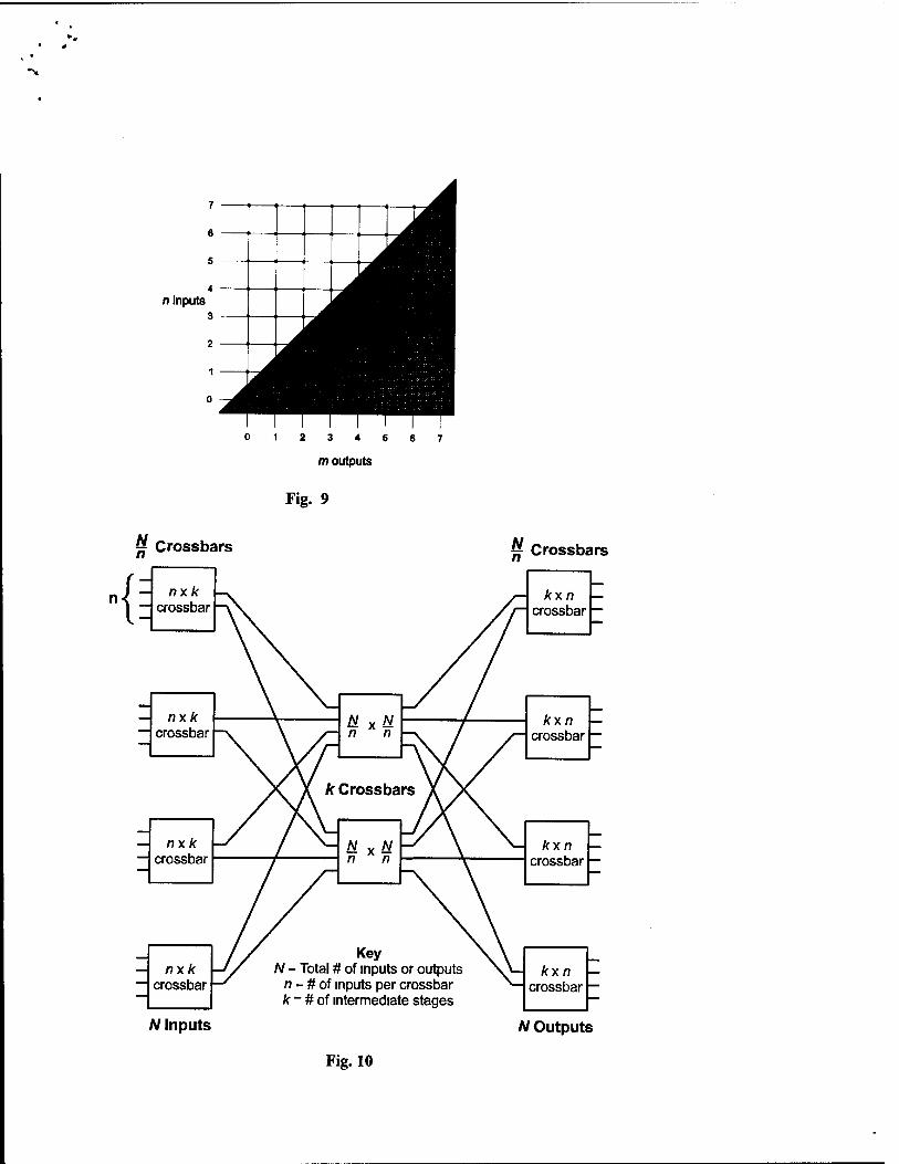
n inputs
0 -^k
12 3 4 5 6 7
m outputs
Fig. 9
^ Crossbars % Crossbars
I — cro! —I nxk
crossbar
— nxk crossbar
nxk crossbar
nxk crossbar
n n
Crossbars
n n
Key # of inputs or outputs
n - # of inputs per crossbar k - # of intermediate stages
/cxn crossbar
/cxn — crossbar —
kxn — crossbar —
kxn crossbar —
N Inputs N Outputs
Fig. 10
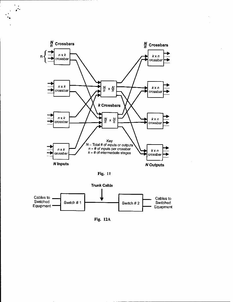
•{ N n Crossbars
nxk crossbar
nxk crossbar
nxk crossbar
nxk crossbar
n n
k Crossbars
N „ N n * n
Key N - Total # of inputs or outputs
n - # of inputs per crossbar k - # of intermediate stages
jjf Crossbars
kxn crossbar
kxn crossbar
kxn crossbar
kxn crossbar
N Inputs N Outputs
Fig. 11
Cables to , Switched
Equipment'
Trunk Cable
I Switch # 1
I Switch # 2
Cables to Switched
Equipment
Fig. 12A
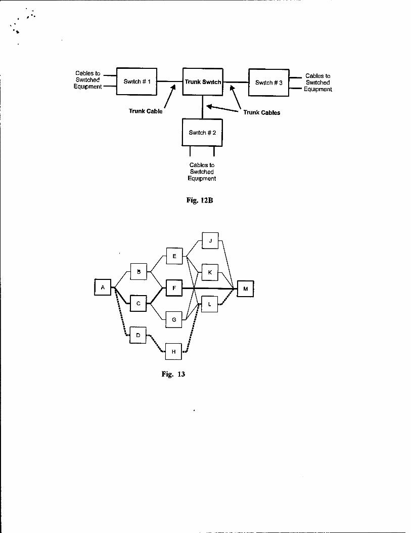
Cables to . Switched
Equipment ■ Switch # 1
Trunk Cable /
Trunk Switch
Switch # 2
i—T Cables to Switched
Equipment
Switch # 3 , Cables to
Switched Equipment
Trunk Cables
Fig. 12B
Fig. 13
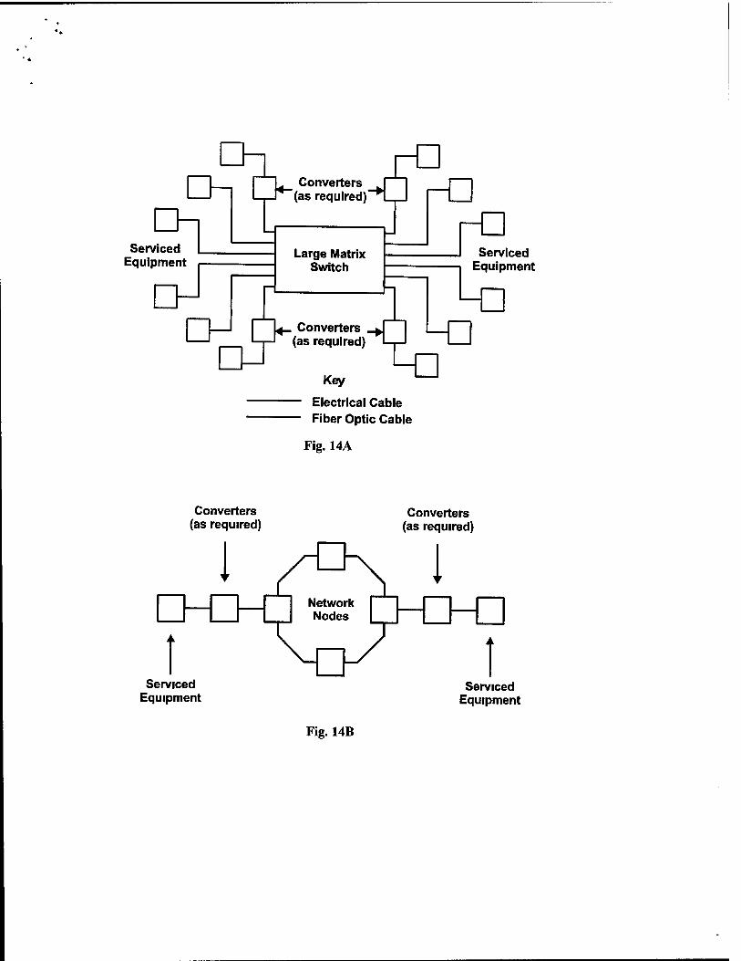
Serviced Equipment
Converters _ "(as required)"
Large Matrix Switch
. Converters . (as required)
Serviced Equipment
Key
- Electrical Cable - Fiber Optic Cable
Fig. 14A
Converters (as required)
1
Converters (as required)
1 i ÜHJ- t
<
s i—i \
Network Nodes
1 -D-D
1 Serviced
Equipment
1 Serviced
Equipment
Fig. 14B
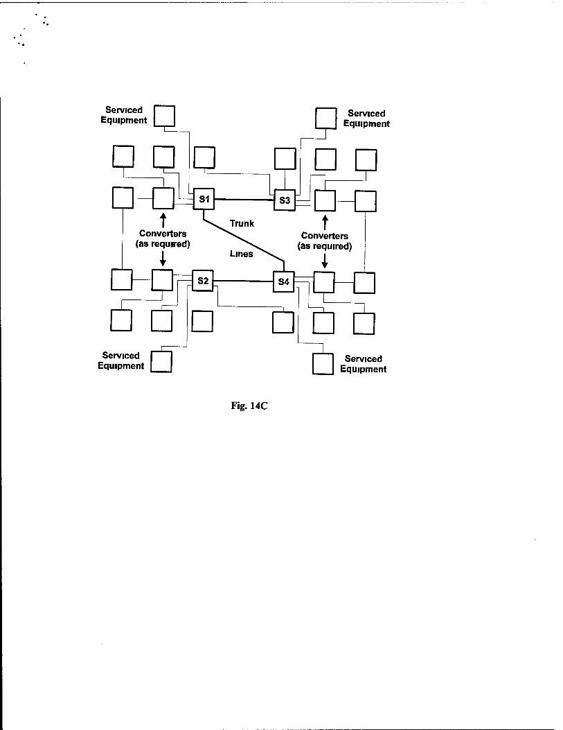
Serviced Equipment
Serviced Equipment
Serviced Equipment
Serviced Equipment
Fig. 14C
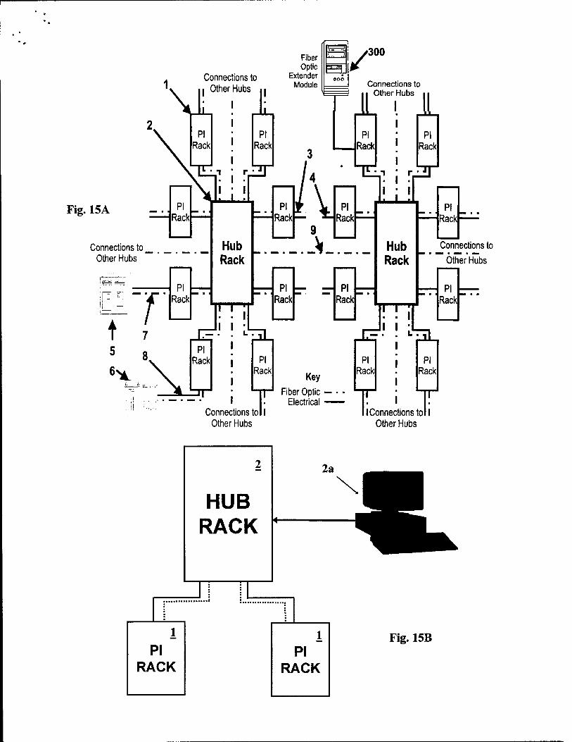
Connections to Other Hubs
Fiber Optic
Extender Module
/30° Connections to
Other Hubs
Fig. 15A -•■/'- *» — Part — PI
Rack
Connections to Other Hubs
Connections to
" Öther'HÜbs
PI Rack
Connections toll Other Hubs
I Connections to 11 Other Hubs
2
HUB RACK
2a
1
PI RACK
1
PI RACK
Fig. 15B
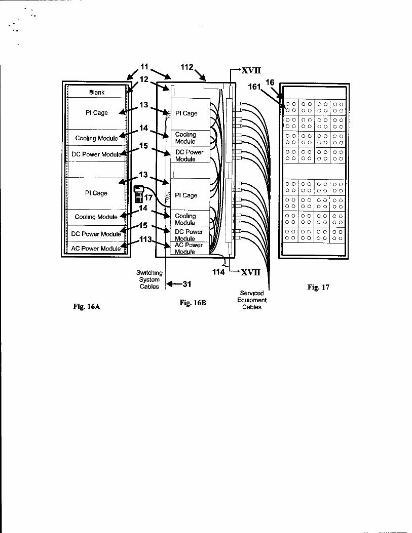
Blank
PI Cage
Cooling Module''
DC Power Module
PI Cage
Cooling Module
/ w
DC Power Module
AC Power Module
11
12
112.
Switching System Cables
PI Cage
Cooling Module
DC Power Module
PI Cage
Cooling Module
DC Power Module AC Power Module
xvn
Fig. 16A
«—31
Fig. 16B Serviced
Equipment Cables
I L° ° O O
o o o o
o o o o
o o o o
O O O O
o o o o
o o o o
o o 0 o
O O o o
o o o o
o o o o
o o o o
o o o o
o o o o
o o o o
o o o o
o o o o
o o o o
o o o o
o o 0 o
o o o o
o o o o
o o o o
o o o o
o o o o
o o o o
o o o o
o o o o
o o o o
o o o o
o o o o
o o o o
Fig. 17
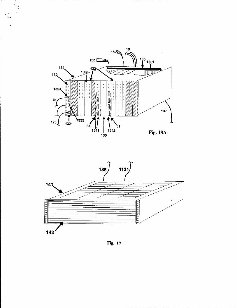
Fig. 18A
Fig. 19
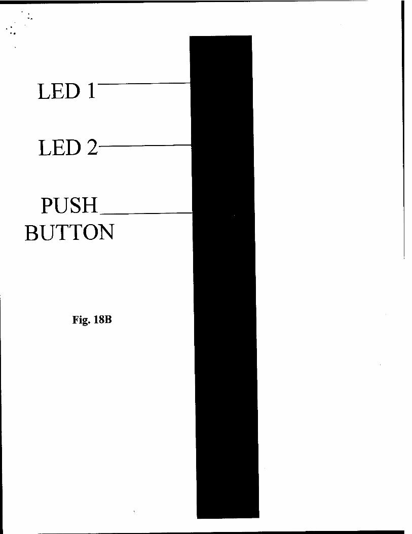
LED1
LED 2
PUSH_ BUTTON
Fig. 18B
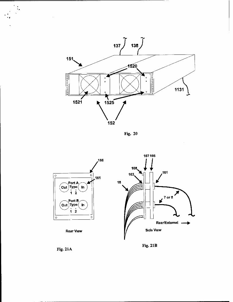
152
Fig. 20
167166
(outVypeMn J
(Out) Type (^ In J
i 2
.166
,161
Rear View
Fig. 21A Fig. 21B
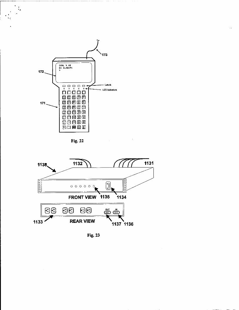
172.
CHNL 1 OK SO ALABAMA
M73
171.
□ □ □ o □ o o o o o ^
DDDOD 111E1 Ulli I11EI
□ QSSS □ 0000 IQill
■ Labels
LED Indicators
Fig. 22
1138
1133 y
-^s rrnr
o o o o o <D
1131
J^s, FRONT VIEW 1135 1134
•z\\*-\ \«z »r vz\\»\ OUT IN
REAR VIEW 1137 1136
Fig. 23
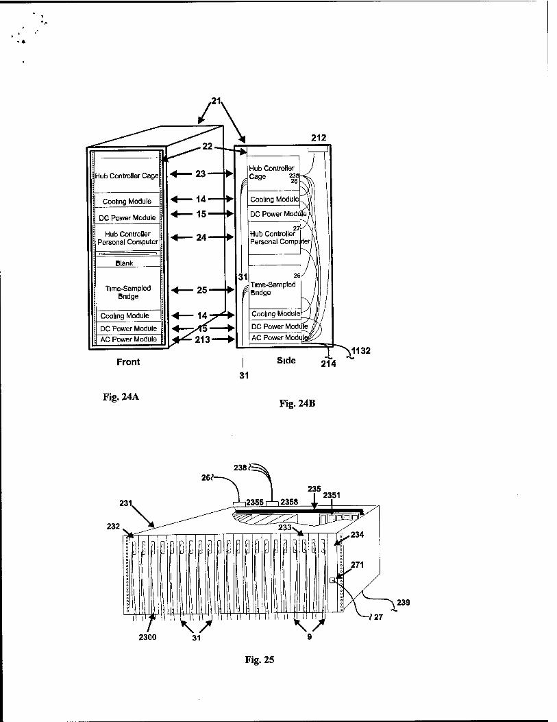
Front Side T^1132 214
31
Fig. 24A Fig. 24B
232
239
Fig. 25
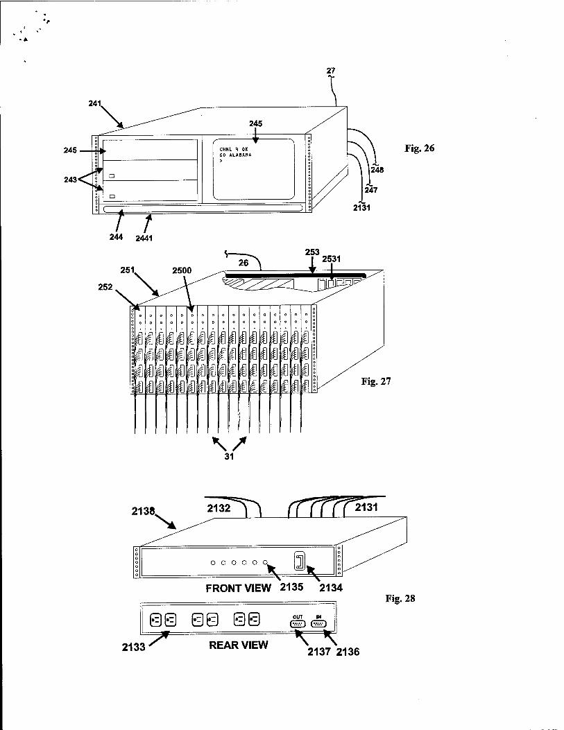
245.
243*
244 2441
252
Fig. 26
253
Fig. 27
2138.
2133 7*
FRONT VIEW 2135 2134
OUT IN
REAR VIEW 2137 2136
Fig. 28
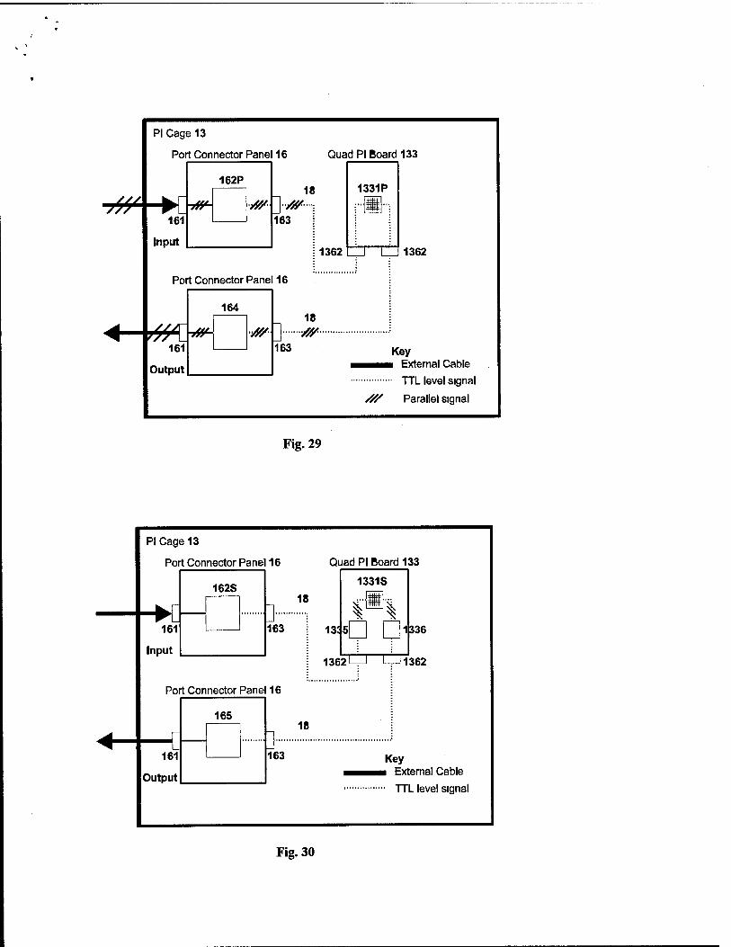
••• ///
PI Cage 13
Port Connector Panel 16 Quad PI Board 133
■>CK 161
Input
162P
163
18
1362
1331P
Port Connector Panel 16
161
Output
164
ifV- 18
'AP\\ /// 163
1362
Key External Cable
TTL level signal
/>y Parallel signal
Fig. 29
PI Cage 13
Port Connector Panel 16 Quad PI Board 133
161
Input
162S
}■ 18
163 132 5
1331S
G D- 1362
Port Connector Panel 16
t 161
Output
165
}■ 18
163
336
1362
Key External Cable
TTL level signal
Fig. 30
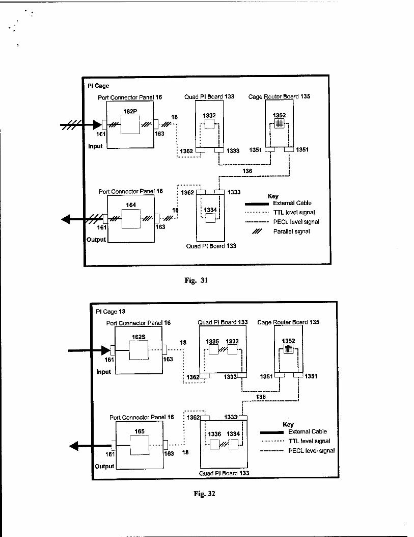
uUA ///
PI Cage
Port Connector Panel 16
161
Input
162P
itP- #/
Quad PI Board 133 Cage Router Board 135
163
18
1362
1332
-Oi
1333 1351
136
1352
1351
Port Connector Panel 16 I 1362
y/j
161
Output
164
^-7*^ /// 18
163
1334: -QJ
1333 Key
i^HM External Cable
TTL level signal
PECL level signal
AP Parallel signal
Quad PI Board 133
Fig. 31
PI Cage 13
Port Connector Panel 16
■W 161
Input
162S
Quad PI Board 133 Cage Router Board 135
} 18
163
1362
1335 1332
rOD"
1333 1351
136
1352
Port Connector Panel 16 j 1362
■C 161
Output
165
> 163 1«
1333f
1336 1334J
-OO1
Quad PI Board 133
1351
Key ■ External Cable
" TTL level signal
- PECL level signal
Fig. 32
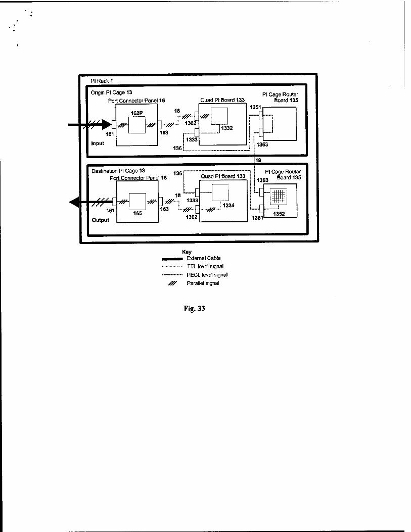
PI Rack 1
Origin PI Cage 13
Port Connector Panel 16
Input
162P
161
18
163
1362
r-Q ■ 1333
136 i
PI Cage Router Quad PI Board 133_ Board 135
1351
A/
J1332
-C-i
1363
19
Destination PI Cage 13 136 j Port Connector Panel 16 i Quad PI Board 133
161
Output
C^ #/
165
0- n 18 ^■■///-.. 1333 163 ■/9T-\_ ■■■■■»?/■■
1362
1334
PI Cage Router
1363 Board 135
1351 ■•['•-- 1352
Key ■ External Cable
TTL level signal
PECL level signal
/// Parallel signal
Fig. 33
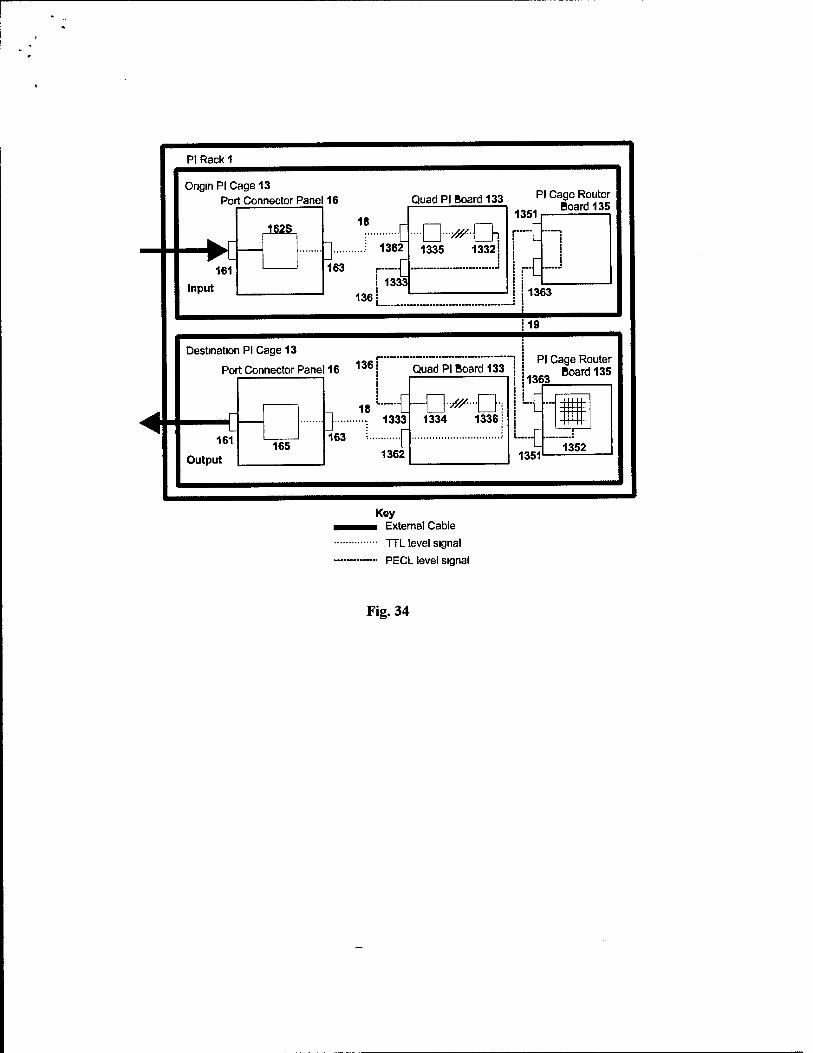
PI Rack 1
Origin PI Cage 13 Port Connector Panel 16
K 161
Input
162S 18
]" 163
136
[ 1362
_[ 1333
Quad PI Board 133 PI Cage Router Board 135
■■D-^-Ch 1335 1332;
1351
-C-J
1363
19
Destination PI Cage 13
Port Connector Panel 16 136! Quad PI Board 133
■c 161
Output 165
> 18 "[
1333 163 -[
1362
1334 1336:
PI Cage Router —« Board 135 1363
-[-
-"[ 1351
1352
Key ■ External Cable
TTL level signal PECL level signal
Fig. 34
MA
Origin PI Rack 1
Port Connector Panel 16
161
Input
162P
■^] 16
163 1362
I Quad PI Board 1331
i 1
1332
0*0 1333L
Four Possible
Paths
136
31
Hub Rack 2
Time-Sampled Bridge 25
TSB Board 252
02522
2523
m 2524
Destination PI Rack 1
Port Connector Panel 16
136
1333 i
-^C 161
Output
164
1&- /&■ > 16
■vff- 163 1362 1334
Four Possible
Paths
Quad PI Board 133
31
Key ■ External Cable TTL level signal PECL level signal
AP Parallel signal Fiber Optic Signal
Fig. 35
136
Option 1
1341
13411
r*0 13412
13413 -► 31
Key
- PECL Level Signal — Fiber Optic Signal
Fig. 36
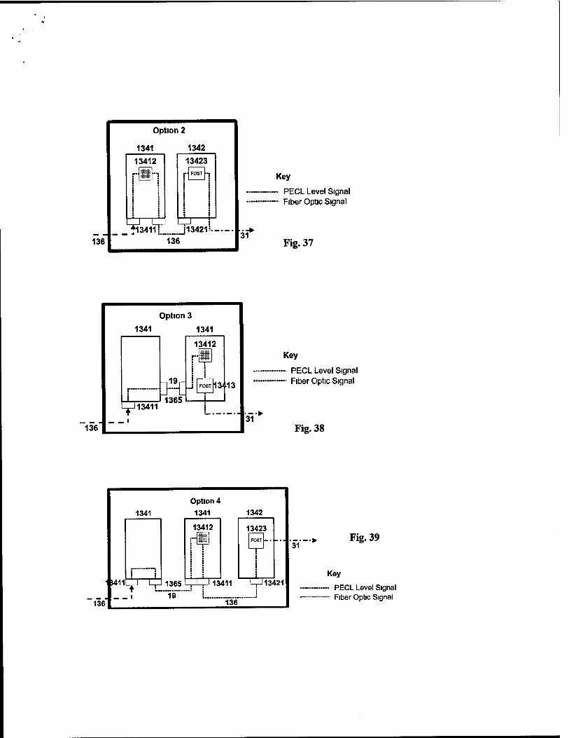
136
Option 2
1341 1342
13412 13423 «■■ FOST ■-■
^pl3411i 136
[13421 ■ 31
Key
- PECL Level Signal — Fiber Optic Signal
Fig. 37
136
1341
Option 3
1341
1365
13' 112
■13
Key
O 1 ,J FOST 13'
sT* LJJ13411
. i ■
Fig. 38
136
Fig. 39
PECL Level Signal Fiber Optic Signal
#
Origin PI Rack 1
Port Connector Panel 16 Quad PI Board 133
>[^ 161
Input
162P
/// 18
] <& [pCh 163 1362
1332
1333L
136
Four Possible
Paths
31
Destination PI Rack 1
Port Connector Panel 16
136
1333 i
IB /&■ ~}~~JW-~{_ rfjQ
1362 1334
Quad PI Board 133
Four Possible
Paths
31
Hub Rack 2
Time-Sampled Bridge 25
TSB Board 252
—-Q 2522
111 | 2523
[roJTJ2524
—i
Key ^^H External Cable
TTL level signal PECL level signal
/P Parallel signal Fiber Optic Signal
Fig. 40
136
Fig. 41
Key
PECL Level Signal Fiber Optic Signal
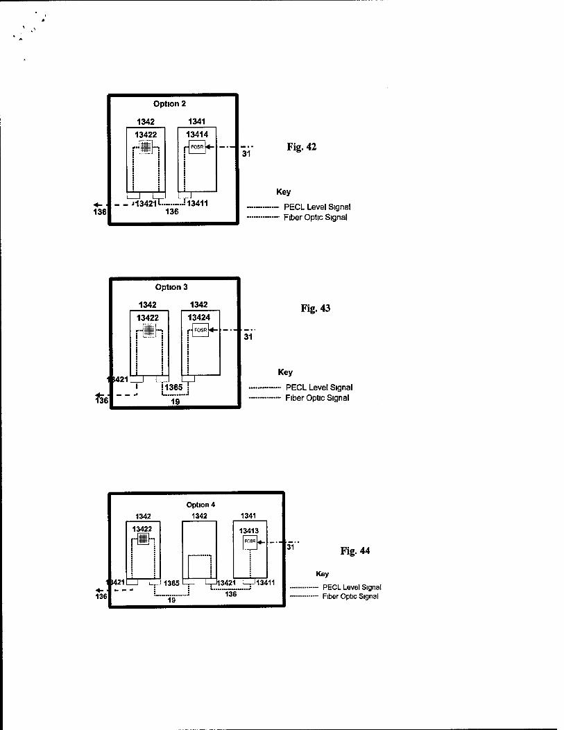
136
Option 2
1342 1341
13422 13414 ri FCSR U-
—I U_ J1342H»
136
1A -i 13411
31 Fig. 42
Key
PECL Level Signal Fiber Optic Signal
Fig. 43
PECL Level Signal ■•• Fiber Optic Signal
Fig. 44
PECL Level Signal Fiber Optic Signal

Ongin PI Rack 1
Port Connector Panel 16
161
Input
162S
Quad PI Board 133
18
] 163 1362
•[
1335
■D
D J1332
1333 U-l
136
Four Possible
Paths
31
Destination PI Rack 1
Port Connector Panel 16
136
1333 r
{ 161
Output
165
p = £ 163 1362
i1334
G I D :1336
Four Possible
Paths
Quad PI Board 133
31
Hub Rack 2
Time-Sampled Bridge 25
TSB Board 252
FOSH 2522
|»J2523
[TOST] 2524
—i
Key ■■■■■ External Cable
TTL level signal
PECL level signal
AP Parallel signal Fiber Optic Signal
Fig. 45
Origin PI Rack 1
Port Connector Panel 16 Quad PI Board 133
161
Input
162S 18
163 ■a
1362
1335 ;•□ a
11332
Four Possible
Paths
13331 136
31
Destination PI Rack 1
Port Connector Panel 16
136 1333
161
Output
165
D " a 163 1362
o. si 334
G I D ■••1336
Quad PI Board 133
Four Possible
Paths
31
Hub Rack 2
Time-Sampled Bndge 25
TSB Board 252
—.|fosR| 2522
lit] 2523 j
[resrJ2524
Key M^H External Cable
TTL level signal
PECL level signal
dy Parallel signal
Fiber Optic Signal
Fig. 46
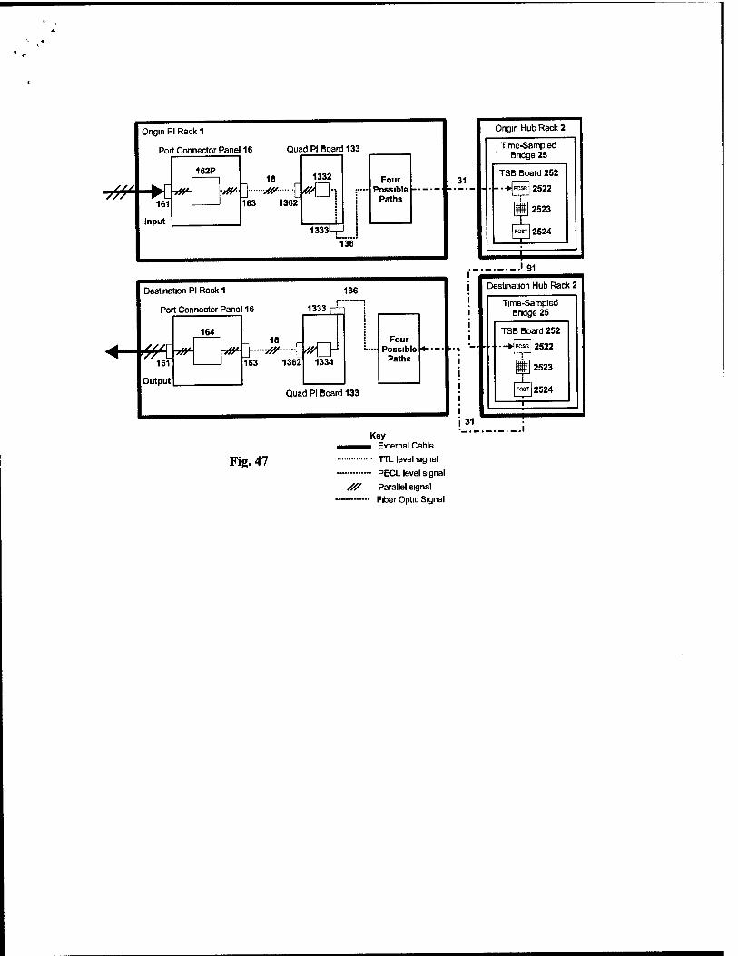
Origin PI Rack 1
Port Connector Panel 16 Quad PI Board 133
1332
[kO
1333L
Four Possible
Paths
136
31
Destination PI Rack 1
Port Connector Panel 16
136
1333 |
•/V 7/ c
161
Output
164
70*" 70" > 18
163 1362 ■EK>
1334
Four Possible
Paths
Quad PI Board 133
Fig. 47
///
Key ■ External Cable
••• TTL level signal
- PECL level signal
Parallel signal
Fiber Optic Signal
Origin Hub Rack 2
Time-Sampled Bridge 25
TSB Board 252
- • - ■ ♦ res» 2522
H 2523
(KSTJ2524
91
31
Destination Hub Rack 2
Time-Sampled Bridge 25
TSB Board 252
►f^J2522
J2523
Rw 2524
■