Embed Size (px)
Citation preview

Ch.1. Introduction R.Klanner: Solid State Detectors - 5.8.05 1.1
DESY Summerstudent’s Lecture 2005:Solid State Detectors
Robert Klanner, University of Hamburg
Chapter 1: Introduction1.1 Aim of Lecture
• Introduction to Solid State (Silicon) Detectors: • Basic principles• Different detector types• Examples for applications• Limitations
Solid state detectors: a rapidly evolving field attempt to present also recent developments
1.2 LiteratureG.Lutz, Semiconductor Detectors, SpringerVarious articles in NIM-A, IEEE-NS, (some references given on slides)
1.3 Index1. Introduction2. Parameters characterising detectors 3. Basics of solid state detectors – interaction of radiation with matter4. Detector types5. Limitations – in particular radiation hardness
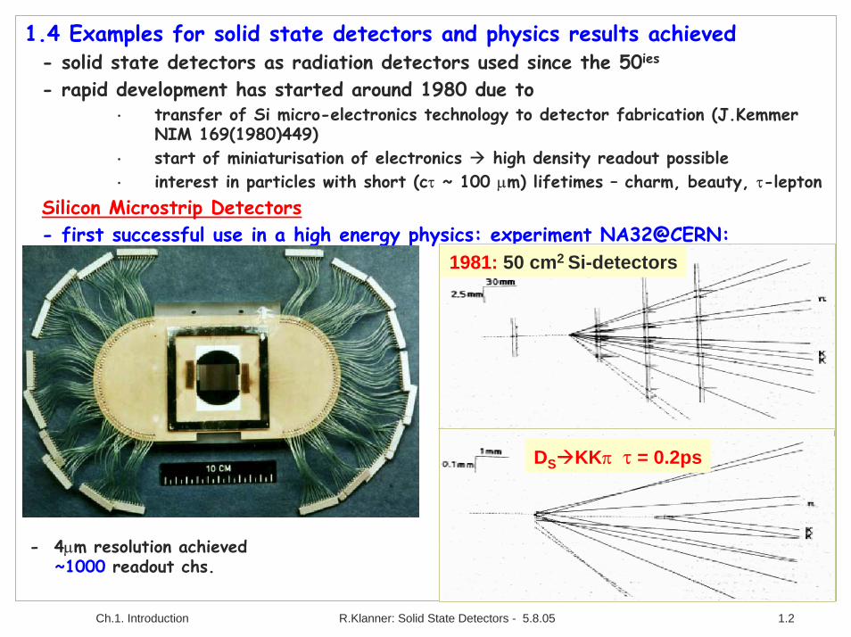
1.4 Examples for solid state detectors and physics results achieved- solid state detectors as radiation detectors used since the 50ies
- rapid development has started around 1980 due to• transfer of Si micro-electronics technology to detector fabrication (J.Kemmer
NIM 169(1980)449)• start of miniaturisation of electronics high density readout possible• interest in particles with short (cτ ~ 100 µm) lifetimes – charm, beauty, τ-lepton
Silicon Microstrip Detectors- first successful use in a high energy physics: experiment NA32@CERN:
1981: 50 cm2 Si-detectors
DS KKπ τ = 0.2ps
- 4µm resolution achieved ~1000 readout chs.
Ch.1. Introduction R.Klanner: Solid State Detectors - 5.8.05 1.2

Silicon Strip Detectoressential for the discovery of the top-quark at FNAL (1994)(and also LEP Higgs limit)
example:CDF vertex detector
- today: CMS@LHC (CERN) ~200m2 and 9.65.106
readout channels
Ch.1. Introduction R.Klanner: Solid State Detectors - 5.8.05 1.3
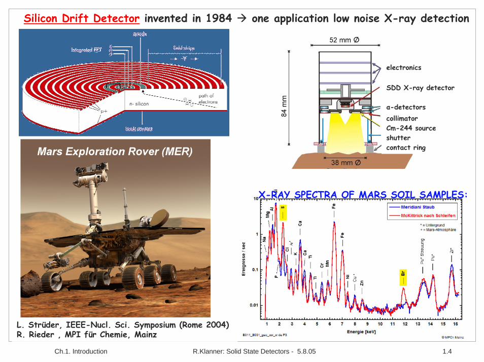
Silicon Drift Detector invented in 1984 one application low noise X-ray detection
electronics
SDD X-ray detector
α-detectorscollimatorCm-244 sourceshuttercontact ring
X-RAY SPECTRA OF MARS SOIL SAMPLES:
L. Strüder, IEEE-Nucl. Sci. Symposium (Rome 2004) R. Rieder , MPI für Chemie, Mainz
Ch.1. Introduction R.Klanner: Solid State Detectors - 5.8.05 1.4

Fully depleted CCD (based on drift chamber principle) – astronomy XXM-Newton
L. Strüder, IEEE-Nucl. Sci. Symposium (Rome 2004)
elemental analysis of TYCHO supernova remnant:
XMM-Newton satellite
Ch.1. Introduction R.Klanner: Solid State Detectors - 5.8.05 1.5

Controlled Drift Detector (CDD) for X-ray radiography
ionizationtrack
back side(p-side)
Tdrift
clock t fast time-of-incidence
anodes (n-side)
X-RAY RADIOGRAPHY:
A. Castoldi et al, NIM-A518(2004)426
Ch.1. Introduction R.Klanner: Solid State Detectors - 5.8.05 1.6
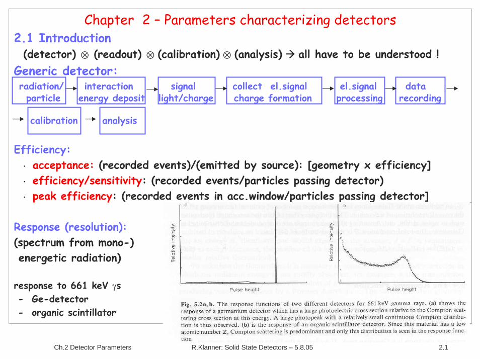
Chapter 2 – Parameters characterizing detectors2.1 Introduction
(detector) ⊗ (readout) ⊗ (calibration) ⊗ (analysis) all have to be understood ! Generic detector:radiation/ interaction signal collect el.signal el.signal data particle energy deposit light/charge charge formation processing recording
calibration analysis
Efficiency:• acceptance: (recorded events)/(emitted by source): [geometry x efficiency]• efficiency/sensitivity: (recorded events/particles passing detector)• peak efficiency: (recorded events in acc.window/particles passing detector]
Response (resolution):(spectrum from mono-) energetic radiation)
response to 661 keV γs- Ge-detector- organic scintillator
Ch.2 Detector Parameters R.Klanner: Solid State Detectors – 5.8.05 2.1
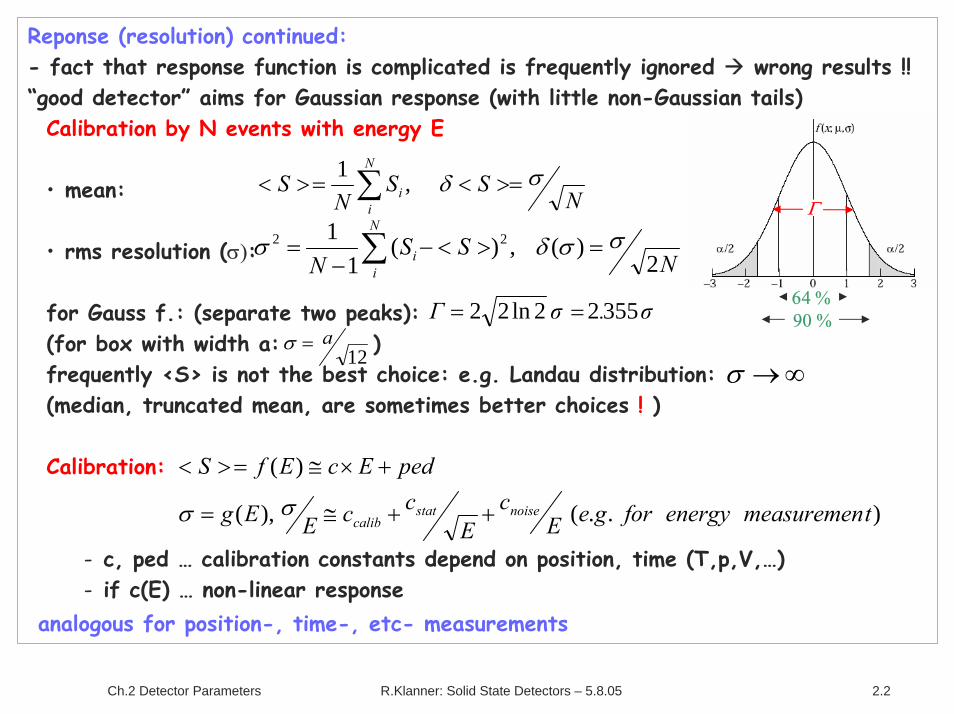
Reponse (resolution) continued:- fact that response function is complicated is frequently ignored wrong results !!“good detector” aims for Gaussian response (with little non-Gaussian tails)
Calibration by N events with energy E
• mean:
• rms resolution (σ):
for Gauss f.: (separate two peaks):(for box with width a: )frequently <S> is not the best choice: e.g. Landau distribution:(median, truncated mean, are sometimes better choices ! )
Calibration:
- c, ped … calibration constants depend on position, time (T,p,V,…)- if c(E) … non-linear response
analogous for position-, time-, etc- measurements
NSS
NS
N
ii
σδ >=<=>< ∑ ,1
∑ =><−−
=N
ii N
SSN 2
)(,)(1
1 22 σσδσ
σ.σΓ 35522ln22 ==
12a=σ
∞→σ
)..(),(
)(
tmeasuremenenergyforgeEc
EccEEg
pedEcEfS
noisestatcalib ++≅=
+×≅=><
σσ
Γ
64 %90 %
Ch.2 Detector Parameters R.Klanner: Solid State Detectors – 5.8.05 2.2
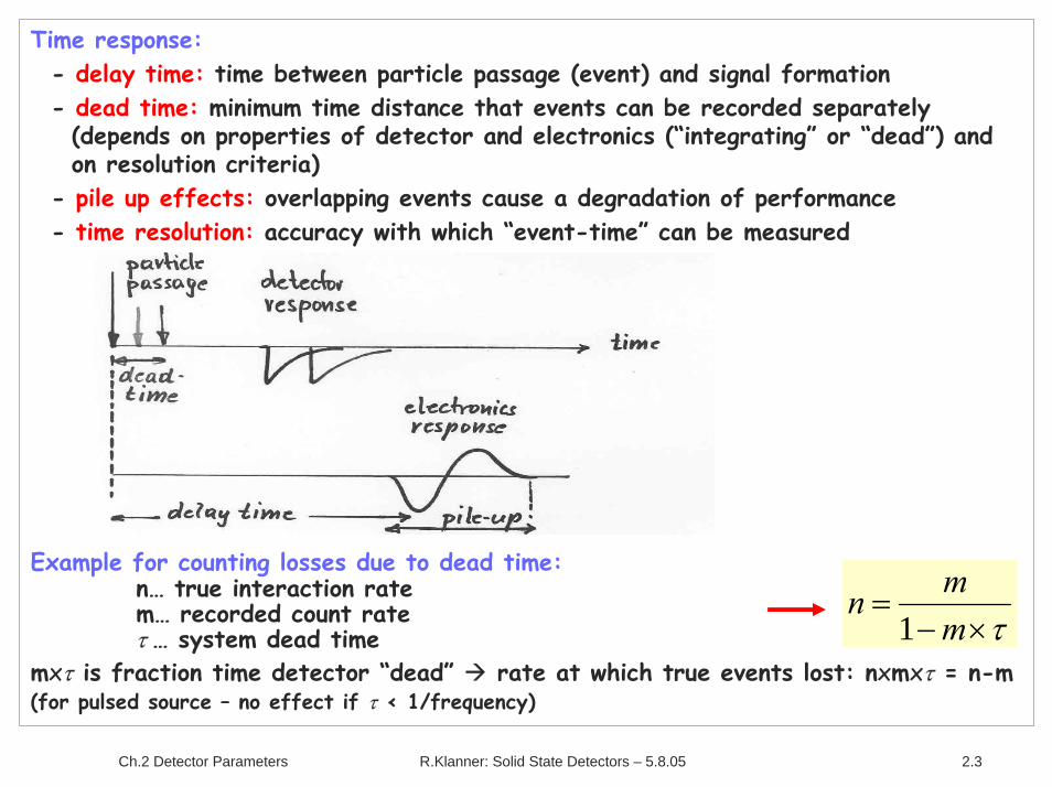
Time response:- delay time: time between particle passage (event) and signal formation- dead time: minimum time distance that events can be recorded separately
(depends on properties of detector and electronics (“integrating” or “dead”) and on resolution criteria)
- pile up effects: overlapping events cause a degradation of performance - time resolution: accuracy with which “event-time” can be measured
Example for counting losses due to dead time:n… true interaction ratem… recorded count rateτ … system dead time
mxτ is fraction time detector “dead” rate at which true events lost: nxmxτ = n-m(for pulsed source – no effect if τ < 1/frequency)
τ×−=
mmn
1
Ch.2 Detector Parameters R.Klanner: Solid State Detectors – 5.8.05 2.3

Examples for pile-up effects:
distortion of spectra (loss in resolution) and overlapping events
situation can be optimized by “clever”electronics – requires understanding of pulse shape produced by detector !
Ch.2 Detector Parameters R.Klanner: Solid State Detectors – 5.8.05 2.4
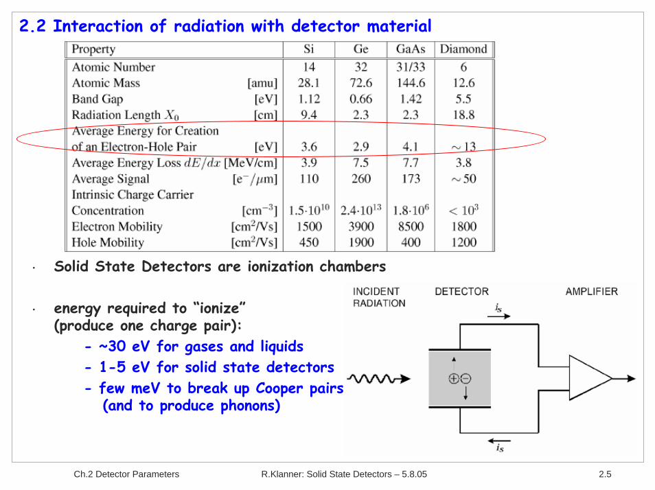
2.2 Interaction of radiation with detector material
• Solid State Detectors are ionization chambers
• energy required to “ionize”(produce one charge pair):
- ~30 eV for gases and liquids- 1-5 eV for solid state detectors- few meV to break up Cooper pairs
(and to produce phonons)
Ch.2 Detector Parameters R.Klanner: Solid State Detectors – 5.8.05 2.5

visible
1 µm
1 mm
well suited fordetection from the UV IR
Detection of light
EGap (Si)
Ch.2 Detector Parameters R.Klanner: Solid State Detectors – 5.8.05 2.6

Detection of charged particles: (dE/dx = energy loss via Coulomb scattering off electrons - ionisation)mean energy loss < dE/dx > – Bethe-Bloch formula vs ß
from dE/dx(MIP):Si: 110 (e-h)/µmGe: 260 (e-h)/µm
“healthy signal”,which can be wellprocessed by elec-tronics
1/v2
log-rise
Ch.2 Detector Parameters R.Klanner: Solid State Detectors – 5.8.05 2.7

Detection of charged particles: fluctuations in dE/dx-distribution
<λSi> = .25µm
Ch.2 Detector Parameters R.Klanner: Solid State Detectors – 5.8.05 2.8

Detection of charged particles: fluctuations in dE/dx-distribution
(H.Bichsel, Rev.Mod.Phys.60(1988)663)shape of energy loss distribution depends on thickness of detector(NB. for thin detectors < 1-2 µm finite probability of zero signal !)
Ch.2 Detector Parameters R.Klanner: Solid State Detectors – 5.8.05 2.9
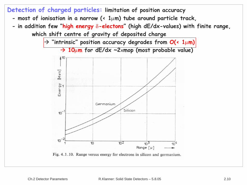
Detection of charged particles: limitation of position accuracy- most of ionisation in a narrow (< 1µm) tube around particle track, - in addition few “high energy δ-electons” (high dE/dx-values) with finite range,
which shift centre of gravity of deposited charge “intrinsic” position accuracy degrades from O(< 1µm)
10µm for dE/dx ~2xmop (most probable value)
Ch.2 Detector Parameters R.Klanner: Solid State Detectors – 5.8.05 2.10

Detection of photons and X-rays: photon attenuation
Si
Ch.2 Detector Parameters R.Klanner: Solid State Detectors – 5.8.05 2.11

Detection of photons and X-rays: required detector thickness
Si and Ge can be used as efficient X-ray detectors for energies up to 30(100) keVfor higher energies high-Z detectors
(eg CdTe, …)
Ch.2 Detector Parameters R.Klanner: Solid State Detectors – 5.8.05 2.12

Detection of photons and X-rays: energy resolution – Fano factor
- mean number of charges for energy deposit E0: NQ=E0/ε (ε … energy required for e-h-pair)
- fluctuations: δNQ=√F.NQ
- if all NQ ionizations independent F = 1- constraints due energy conservation F < 1
(simple model U.Fano Phys.Rev.72(1947)26 with a number of ad hoc assumptions: F = EX/EGap
.(ε/EGap-1) (EX … mean energy of phonon excitation, EGap … band gap)- example Si:
- EGap= 1.1 eV- EX = 0.037 eV- ε = 3.6 eV
F = 0.08δNQ=0.3√NQ
significant im-provement of δE
Ch.2 Detector Parameters R.Klanner: Solid State Detectors – 5.8.05 2.13

Chapter 3: Basics of Solid State Detectors3.1 Principle
• Solid State Detectors are ionization chambers
• any material which allows charge collection can be used for an ionization chamber
• energy required to “ionize” (produce one charge pair):- ~30 eV for gases and liquids- 1-5 eV for solid state detectors- few meV to break up cooper pairs (and to produce phonons)
advantages solid state d.: efficient, density, room temperature operation, highly developed µ-technology, robust devices, well suited for µ-electronics readout
Ch.3. Basics of Solid State Detectors R.Klanner: Solid State Detectors - 5.8.05 3.1
Ch.3. Basics of Solid State Detectors R.Klanner: Solid State Detectors - 5.8.05 3.2
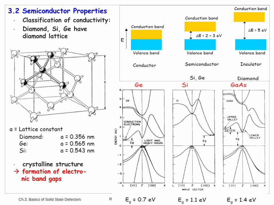
3.2 Semiconductor Properties• Classification of conductivity:• Diamond, Si, Ge have
diamond lattice
• crystalline structure formation of electro-nic band gaps
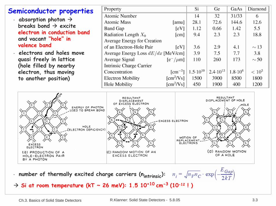
Semiconductor properties• absorption photon
breaks bond exciteelectron in conduction bandand vacant “hole” in valence band
• electrons and holes movequasi freely in lattice(hole filled by nearby electron, thus movingto another position)
• number of thermally excited charge carriers (nintrinsic):
Si at room temperature (kT ~ 26 meV): 1.5 10+10 cm-3 (10-12 ! )
Ch.3. Basics of Solid State Detectors R.Klanner: Solid State Detectors - 5.8.05 3.3

Mobility µ: electrons and holes drift under the influence of electric field E:• for low fields (Si < 5kV/cm)
• for high fields v ~ 107cm/scharge collection times for300µm Si detector: O (10ns)
• drift in magnetic fieldLorentz angle: tanθ=µHall
.BTHall mobility:electrons: µHall=1650cm2/Vsholes µHall = 310cm2/Vs~30° for 4 Tesla field (e)(165 µm shift for 300 µm)
Diffusion D:• Einstein relation: D=(kT/q).µ
spread of charge after time t:σ2 = 2.D.t6 µm for 10ns drift of electrons
Resistivity ρ: defined by (J … current density)for semiconductors with both electrons (n) and holes (p) as carriers:n … density of electrons, p … density of holes
resistivity of intrinsic Si at room temperature: 230 kΩ cm
mobilityEv ..., µµvv =
JEvv
⋅= ρ)(
1pnq pn ⋅+⋅
=µµ
ρ
Ch.3. Basics of Solid State Detectors R.Klanner: Solid State Detectors - 5.8.05 3.4
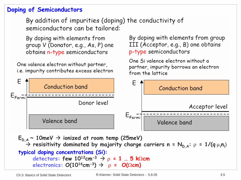
Doping of Semiconductors
ED,A ~ 10meV ionized at room temp (25meV) resisitivity dominated by majority charge carriers n = ND,A: ρ = 1/(q µini)
typical doping concentrations (Si):detectors: few 1012cm-3 ρ = 1 … 5 kΩcmelectronics: O(1016cm-3) ρ = O(Ωcm)
Ch.3. Basics of Solid State Detectors R.Klanner: Solid State Detectors - 5.8.05 3.5

Doping of Semiconductors
Ch.3. Basics of Solid State Detectors R.Klanner: Solid State Detectors - 5.8.05 3.6

3.3 How to build a solid state ionization chamber – the pn junction
- thermal diffusion drives electrons and holes across pn junctiongeneration of depletion regions (no free charge carriers) with fixed space charge
- potential and electric field obtained from Poisson’s equation:- diffusion potential (built-in potential Vbi) obtained by EFermi = const over junction
for Si one-sided abrupt junction Vbi~0.65V for n doping few 1.4.10+12cm-3 (3 kΩcm) depth of depletion region: d ~ 25 µm
ερ )(
2
2 xdxdE
dxVd
==−
field linear in xpotential quadratic in x
Ch.3. Basics of Solid State Detectors R.Klanner: Solid State Detectors - 5.8.05 3.7
Ch.3. Basics of Solid State Detectors R.Klanner: Solid State Detectors - 5.8.05 3.8
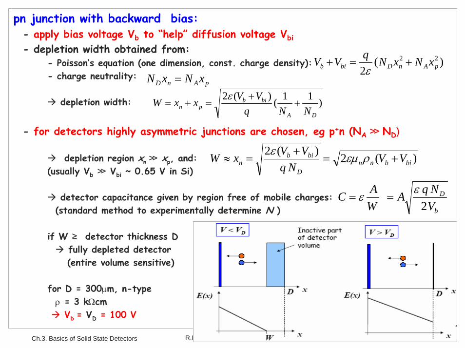
pn junction with backward bias:- apply bias voltage Vb to “help” diffusion voltage Vbi
- depletion width obtained from:- Poisson’s equation (one dimension, const. charge density):- charge neutrality:
depletion width:
- for detectors highly asymmetric junctions are chosen, eg p+n (NA ≫ ND)
depletion region xn ≫ xp, and:(usually Vb ≫ Vbi ~ 0.65 V in Si)
detector capacitance given by region free of mobile charges: (standard method to experimentally determine N )
if W ≥ detector thickness Dfully depleted detector (entire volume sensitive)
for D = 300µm, n-type ρ = 3 kΩcm
Vb = VD = 100 V
)(2
22pAnDbib xNxNqVV +=+
εpAnD xNxN =
)11()(2
DA
bibpn NNq
VVxxW ++
=+=ε
)(2)(2bibnn
D
bibn VV
NqVVxW +=
+=≈ ρεµε
b
D
VNqA
WAC
2εε ==

electric field in over-depleted pn junction and charge collection time:- depletion voltage:
- electric field at x = D:
- drift:
- time needed for charge carriers to traverse entire detector:
for D = 300µm, n-type ρ = 3 kΩcm, Vb = 200 V: tdrift(n) = 3.5 ns, tdrift(p) = 11 ns
2
2DNqV D
D ε=
DVVDE Db /)()( −=
DVV
Dx
DVxE DbD −
+⎟⎠⎞
⎜⎝⎛ −= 12)(
∫=→= 2
1 )(),()()( 21
x
x xvdxxxtxExv µ
bi
VV
Db
D
Didrift V
DVV
VV
Dt Db
µµ
22 21ln
2⎯⎯⎯ →⎯⎟⎟
⎠
⎞⎜⎜⎝
⎛−
+= >>
Ch.3. Basics of Solid State Detectors R.Klanner: Solid State Detectors - 5.8.05 3.9

3.4 Signal formation in planar pn diode:- signal in electrodes by induction
(not arrival of charge at electrodes !)- electrodes (example parallel plates)
via low Z amplifier at const. potential- electrostatic problem can be solved
by ∞ no. of image charges- moving charge changes charge profile
induces detectable signal- problem can also (and best) be solved by method of weighting fields
-example: charge pair +/-q produced at x0
- induced current:
- total chargeinduced by –q
induced by +q
sum(total charge q independent of starting point x0)
- situation more complicated when electrodes are segmented (eg strip detectors)
d
(Q q)
x0d q
qQQQ
xddqdx
dqQ
xdqdx
dqQ
dvq
dtdQI
x
d
x
−=+=
−−=+
−=
−=−
−=
−==
+−
+
−
∫
∫
)( 0
0
0
0
0
Ch.3. Basics of Solid State Detectors R.Klanner: Solid State Detectors - 5.8.05 3.10
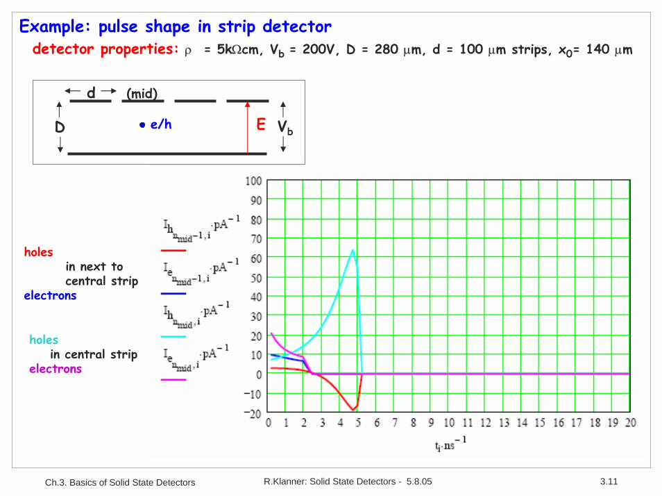
Example: pulse shape in strip detectordetector properties: ρ = 5kΩcm, Vb = 200V, D = 280 µm, d = 100 µm strips, x0= 140 µm
holesin next to central strip
electrons
holesin central strip
electrons
D
d
Ee/h
(mid)
Vb
Ch.3. Basics of Solid State Detectors R.Klanner: Solid State Detectors - 5.8.05 3.11
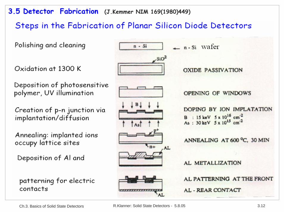
3.5 Detector Fabrication (J.Kemmer NIM 169(1980)449)
Ch.3. Basics of Solid State Detectors R.Klanner: Solid State Detectors - 5.8.05 3.12

Ch.4 Detector TypesSolid state detectors:
- “efficient” (Si: 3.6 eV/e-h pairs) + high density large signal
- high speed (~ 10 nsec)- highly developed technology (micro-
electronics) accuracy (µm) + reliability (if properly designed !)
- reasonably rad.hard (~1015n/cm2)- possibility to integrate electronics- no internal gain needed stability
but: limited size + fairly high cost4.1 Low Noise Electronics
- most detectors rely critically on fast low-noise electronics
- major progress due to development of low-power/low-noise micro-electronics
Cd … detector (model – Rd !)Rb … biasing resistorCC … blocking capacitorRS … all resistors in input path
- model (equivalent circuit) for noise analysis:
ind … leakage current (det. noise)inb … Rb shunt resistor noiseina … amplifier current noiseens … series resistor voltage noiseena … amplifier voltage noiseinterplay detector -- read-out
Ch.4 Detector Types R.Klanner: Solid State Detectors 4.8.05 4.1
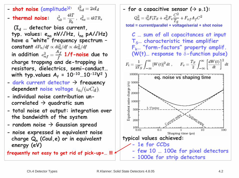
- shot noise (amplitude)2:
- thermal noise:
(Id … detector bias current, typ. values: ena nV/√Hz, ina pA/√Hz) have a “white” frequency spectrum –constantin addition 1/f-noise due tocharge trapping and de-trapping in resistors, dielectrics, semi-conduct… with typ.values Af = 10-10…10-12V2 )
- dark current detector frequency dependent noise voltage
- individual noise contribution un-correlated quadratic sum
- total noise at output: integration over the bandwidth of the system
- random noise Gaussian spread- noise expressed in equivalent noise
charge Qn (Coul,e) or in equivalent energy (eV)
frequently not easy to get rid of pick-up+… !!!
- for a capacitive sensor ( p.1):
C … sum of all capacitances at input TS… characteristic time amplifier Fk… “form-factors” property amplif. (W(t)… response to δ-function pulse)
typical values achieved:- 1e for CCDs- few 10 … 100e for pixel detectors- 1000e for strip detectors
eq. noise vs shaping time
total = current/parallel + voltage/serial + shot noise
Ch.4 Detector Types R.Klanner: Solid State Detectors 4.8.05 4.2
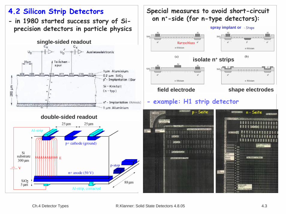
4.2 Silicon Strip Detectors- in 1980 started success story of Si-
precision detectors in particle physics
Special measures to avoid short-circuit on n+-side (for n-type detectors):
- example: H1 strip detector
single-sided readout
double-sided readout
isolate n+ strips
field electrode shape electrodes
spray implant or
Ch.4 Detector Types R.Klanner: Solid State Detectors 4.8.05 4.3

spatial resolution: strip pitch with interpolation by diffusion (~10 µm)
measureddistributionof holes atp+ strips
achieved resolution: ~ 1µm (detector with 20µm pitch NIM235(1985)210)
- coupling of detectors to reduce no. of readout channels (ladders)
comparison sizeof diff. vertex det.
Ch.4 Detector Types R.Klanner: Solid State Detectors 4.8.05 4.4

Si-vertex detectors: complex, high-tech detectors – e.g SVXII for CDF
CMS-tracking: world’s largest Si-det.!
Si-vertex detectors at DESY (HERA):H1 FST (Forward Silicon Tracker)
ZEUS MVD (MicroVertex
Detector)at DESY
CMS: 200m2
Si-detectors!
2007: LHC@CERN6 m
Ch.4 Detector Types R.Klanner: Solid State Detectors 4.8.05 4.5

4.3 Solid State Drift ChambersPrinciple (like back-to-back diodes):
potential distribution
segmented anode 2(3)-d measurementC-V characteristicsof Si-drift chamber
Ch.4 Detector Types R.Klanner: Solid State Detectors 4.8.05 4.6

- first realisation (NIM235(1985)231)
- position resolution vs drift field ~ 5µm achieved
example of a vertex detector based on Si-drift chambers (STAR detector at RHIC, BNL – NIMA 541(2005)57)
- excellent 2d position resolution with small no. of read-out channels but
- speed (several 100 ns drift times)- sensitivity to radiation
drift principle many applications!
Laser spot beam particles
Ch.4 Detector Types R.Klanner: Solid State Detectors 4.8.05 4.7

high resolution X-ray detector:to profit from low C: on detector FET
energy resolution: 121eV@6keV (-10°)
Pixel Detectors:4.4 Charged Coupled Devices (CCD)
principle of operation:
55Fe-spectrum – δE close to theor. limit!
Ch.4 Detector Types R.Klanner: Solid State Detectors 4.8.05 4.8

CCD principle of operation
- many (106) pixels – small no. of channels- excellent noise performance (few e)- small pixel size (e.g. 22x22 µm2)- slow (many ms) readout time- sensitive during read-out- radiation sensitive
used at SLC best vertex detector so far with 3x108 pixels !!!
technological realisation:
Ch.4 Detector Types R.Klanner: Solid State Detectors 4.8.05 4.9

Ch.4 Detector Types R.Klanner: Solid State Detectors 4.8.05 4.10
SLC Vertex detector:
further developments:- fully depleted CCDs for X-ray
measurements- thinning to ~50 µm to reduce multiple
scattering + sec. interactions- read-out of every column separately
with 50MHzapplications outside HEP RR
bbZ →0

R&D on CCDs for ILC vertex detector (LCFI-collab. – DESY PRC 26.5.05)
very ambitious:
20µm pixelsδx~3µm
109 pixels
60µm thick “unsupported”
50µs read-out(50 MHz!)
noise: 60e
Text
CPCCD1 bonded module
Ch.4 Detector Types R.Klanner: Solid State Detectors 4.8.05 4.11

4.5 Hybrid Pixel DetectorsPrinciple: separate detector-electronics
Summary Hybrid Pixel Detectors- technology well developed, m2s used in
LHC-experiments (ALICE, ATLAS, CMS), synchrotron rad., radiology,…
- already experience in actual experi-ments
- high degree of flexibility in design many developments in progress !
- radiation hardness achieved,- “any” detector material possible (Si,
GaAs, CdTe,…)- typical pixel dimensions > 50 µm,- high speed: e.g. 1 MHz/pixel,- (effective) noise ~100e achieved- limitations for particle physics is
detector thickness, power and possibly minimum pixel size
particles
bump-bonding
Ch.4 Detector Types R.Klanner: Solid State Detectors 4.8.05 4.12

Ch.4 Detector Types R.Klanner: Solid State Detectors 4.8.05 4.13
4.6 Monolithic Pixel DetectorsIdea: radiation detector + amplifying +
logic circuitry on single Si-wafer- dream! 1st realisation already in 1992- strong push from ILC minimum
thickness, size of pixels and power !- so far no large scale application in
research (yet)CMOS Active Pixels(used in commercial CMOS cameras)Principle:
- technology in development – with many interesting results already achieved
example: MIMOSA (built by IReS-Strasbourg; tests at DESY + UNIHH)
3.5 cm2 produced by AMS (0.6µm)14 µm epi-layer, (17µm)2 pixels4 matrices of 5122 pixels10 MHz read-out ( 50µs)120 µm thick
output
reset transistor
collectingnode
not depleted
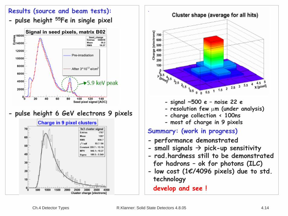
Results (source and beam tests):- pulse height 55Fe in single pixel
- pulse height 6 GeV electrons 9 pixels
- cluster shape
- signal ~500 e – noise 22 e- resolution few µm (under analysis)- charge collection < 100ns- most of charge in 9 pixels
Summary: (work in progress)- performance demonstrated- small signals pick-up sensitivity- rad.hardness still to be demonstrated
for hadrons – ok for photons (ILC)- low cost (1€/4096 pixels) due to std.
technologydevelop and see !
Ch.4 Detector Types R.Klanner: Solid State Detectors 4.8.05 4.14

DEPFET Pixel Detectors
- sideward depletion (Si-drift chamber) - potential minimum for e- ~1µm underneath
transistor channel by “deep” n-implant- transistor channel steered by external gate
and by internal gate- very low C (~fF) low noise (2e for circu-
lar structure, 10 e for linear structure)- achieved amplifications ~400pA/e (int.gate)
“outstanding” performance R&D for:- vertex detectors- X-ray astronomy- SR-research- biomedical applications
50-500µmLayout of an ILC Vertex Detector
- 5 cylindrical layers (L0 L4)- variable pixels 20µm(L0) - 40µm(L4)- reduce readout t 25µs(L0) – 50µs(L1)- <Power> 3-30W (dep. on duty cycle)
Ch.4 Detector Types R.Klanner: Solid State Detectors 4.8.05 4.15

Matrix readout (ILC 13x100mm2 25µm2 pixels-5W):
- connect gates/clears horizontally to select/clear signal rows
- connect drains(+sources) vertically and amplify I or V no shift of charge !!!
- sequence: enable row read (Isig+Iped) clear subtract (Iped) next row
- read 10x2048 rows in 50 ns (20 MHz)
4.7 Summary- starting with Si-strip detectors in
1980 Si-detectors became a central tool in particle physics, SR research, medical applications,… are following
- R&D driven (and most advanced) in particle physics – it still has to be demonstrated if these developments also satisfy the requirements of the new generation of X-ray sources
- if you are interested in detectors that’s the field to join !
- European (also German) groups are leading the field
- lecture gave only a small overview see e.g. NIMA541(2005)1-466, NIMA521(2003)1-452 + many on-going conferences and workshops
Ch.4 Detector Types R.Klanner: Solid State Detectors 4.8.05 4.16

Chapter 5: Limitations of Silicon Detectors5.1 Limitations due to technology:
• Size: Detectors require high quality single crystals 200 mm Ø probably limit• Thickness: Limitation due to maximum voltage (field); up to O(1mm) no problem,
above special care (+cost due to special manufacturing)• Cost: Is clearly a significant issue – but CMS has a >200m2 Si-tracking
detector!• Number of Channels: limitation does not come from detectors but from read-out
power, and connection techniques many innovative ideas5.2 Limitations due to radiation hardness:
- appears at present most serious limitationin particle physics (at high energy hadron colliders, like the TeVatron and the LHC)
- requirements: O(3.1015n-equ./cm2) for 10 years LHCfor SLHC (LHC-luminosity upgrade afactor x10 higher!
present day (under installation at LHC)Si-detectors do not meet requirements(exchange of pixel detectors at LHC)
0 10 20 30 40 50 60R [cm]
1012
1013
1014
1015
Φeq
[cm
-2] total Φeq
neutrons Φeq
pions Φeq
other chargedhadrons Φeq
SCT - barrelSCT - barrelPixelPixel
3x1014cm-23x1014cm-2
SCT - barrelSCT - barrel
PixelPixel
Yearly dose at LHC
Ch.5. Detector Limitations R.Klanner: Solid State Detectors - 5.8.05 5.1

Basic Damage effects: Creation of Primary Defects
primary defects unstable defect kinetics results in secondary defect generationradiation damage a complex, multi-parameter problem
Ch.5. Detector Limitations R.Klanner: Solid State Detectors - 5.8.05 5.2

Change of macroscopic properties of Si due to radiation damage
*)
*) at LHC the limiting effect bias voltage > breakdown voltage of detectors(increase in leakage current reduced by T~-10°C (I~exp(-EGap/2kT)) Ch.5. Detector Limitations R.Klanner: Solid State Detectors - 5.8.05 5.3
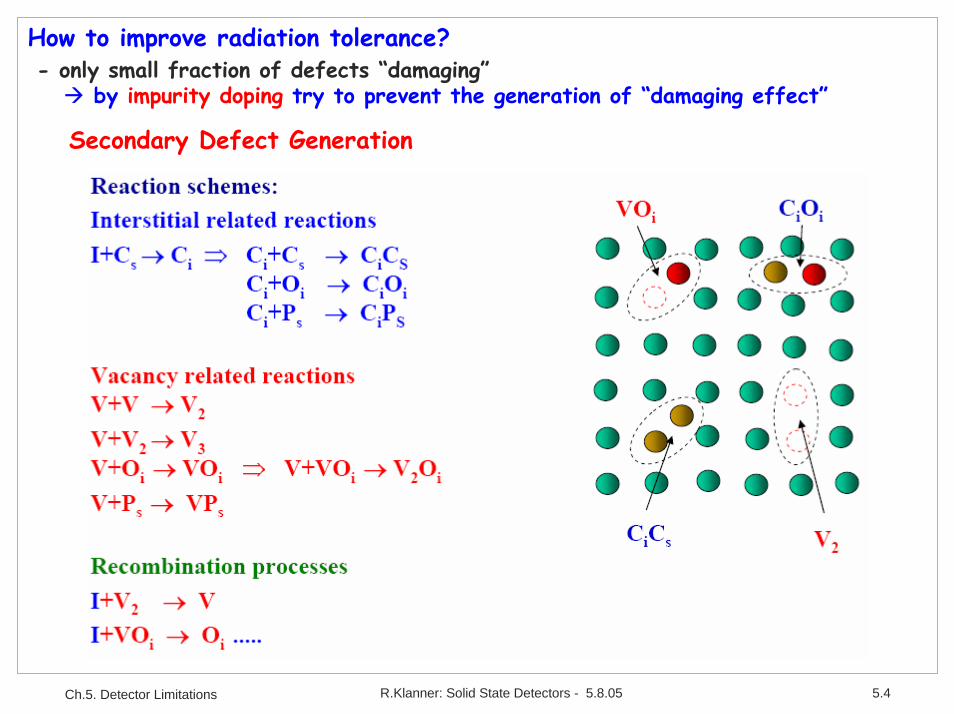
How to improve radiation tolerance? - only small fraction of defects “damaging”
by impurity doping try to prevent the generation of “damaging effect”
Secondary Defect Generation
Ch.5. Detector Limitations R.Klanner: Solid State Detectors - 5.8.05 5.4

How to improve radiation tolerance?
• requires the understanding of the relation between microscopic damages and macroscopic effects
• detailed and complex solid state measurements• precise understanding of material and production technology• complicated by the fact that only small fraction of damages “harmful”
Ch.5. Detector Limitations R.Klanner: Solid State Detectors - 5.8.05 5.5
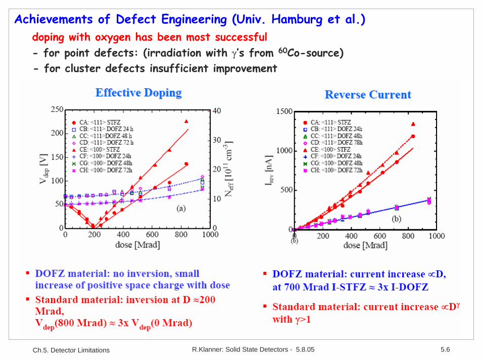
Achievements of Defect Engineering (Univ. Hamburg et al.)doping with oxygen has been most successful- for point defects: (irradiation with γ’s from 60Co-source)- for cluster defects insufficient improvement
Ch.5. Detector Limitations R.Klanner: Solid State Detectors - 5.8.05 5.6

Achievements of Defect Engineering (Univ. Hamburg et al.) for point + cluster defects: (irradiation with 24 GeV/c protons)
major success for EPI-Si (50µm) on Cz-grown Si
radiation tolerance of material for a detector at SLHC at 4cm from beam appears to be demonstrated (but still lot’s of work until realised in a detector)
Ch.5. Detector Limitations R.Klanner: Solid State Detectors - 5.8.05 5.7