Embed Size (px)
Citation preview

RAPID COMMUNICATIONS
PHYSICAL REVIEW B 86, 081301(R) (2012)
Robust optical emission polarization in MoS2 monolayers through selective valley excitation
G. Sallen,1 L. Bouet,1 X. Marie,1 G. Wang,2 C. R. Zhu,2 W. P. Han,3 Y. Lu,3 P. H. Tan,3 T. Amand,1
B. L. Liu,2,* and B. Urbaszek1,†1Universite de Toulouse, INSA-CNRS-UPS, LPCNO, 135 Avenue de Rangueil, 31077 Toulouse, France
2Beijing National Laboratory for Condensed Matter Physics, Institute of Physics, Chinese Academy of Sciences, Beijing 100190, China3State Key Laboratory of Superlattices and Microstructures, Institute of Semiconductors, Chinese Academy of Sciences, Beijing 100083, China
(Received 26 June 2012; published 6 August 2012)
We report polarization resolved photoluminescence from monolayer MoS2, a two-dimensional, noncentrosym-metric crystal with direct energy gaps at two different valleys in momentum space. The inherent chiral opticalselectivity allows exciting one of these valleys, and close to 90% polarized emission at 4 K is observed with 40%polarization remaining at 300 K. The high polarization degree of the emission remains unchanged in transversemagnetic fields up to 9 T indicating robust, selective valley excitation.
DOI: 10.1103/PhysRevB.86.081301 PACS number(s): 78.60.Lc, 78.66.Li
Introduction. The spectacular progress in controlling theelectronic properties of graphene1,2 has triggered researchin alternative atomically thin two-dimensional crystals. Heremonolayer (ML) MoS2 [see the structure in the inset ofFig. 3(a)] has emerged as a very promising material foroptical and spin applications for mainly two reasons. First,the indirect bulk semiconductor MoS2 becomes direct whenthinned to 1 ML,3–5 resulting in efficient optical absorption andemission3–6 and promising reports on using ML MoS2 as anactive field effect transistor (FET) channel.7 Second, inversionsymmetry breaking (usually absent in graphene) together withthe spin-orbit interaction leads to a coupling of carrier spinand k-space valley physics, i.e., the circular polarization (σ+or σ−) of the absorbed or emitted photon can be directlyassociated with selective carrier excitation in one of the twononequivalent k valleys (K+ or K−, respectively). This chiraloptical valley selectivity has been theoretically predicted8–10
with very recent encouraging experimental results reportingindeed strong polarization of the photoluminescence (PL)emission in ML MoS2.9,11,12
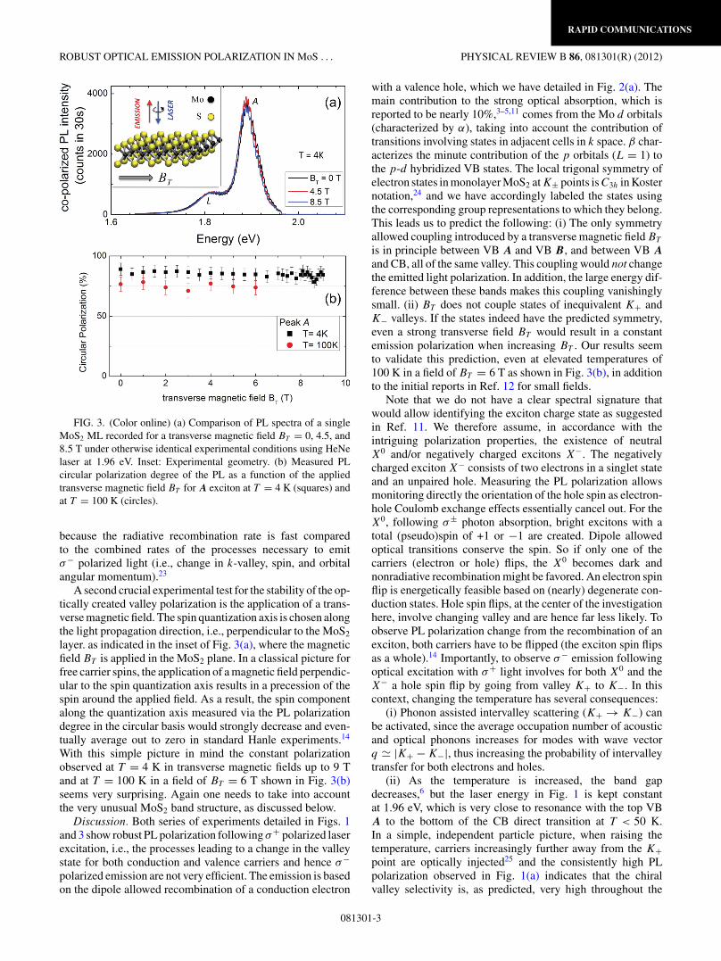
The selection rules for the direct, dipole allowed opticaltransitions in a MoS2 ML are represented in Fig. 2(a). Theconduction band (CB) minimum located at the K− and K+points is spin degenerate.13 In contrast, at the valence band(VB) maximum, also located at the K± points, spin-orbitcoupling induces a splitting between spin up and spin downbands of about 150 meV due to the absence of inversionsymmetry in monolayer MoS2.8 Therefore at low temperaturesa spin flip to the opposite spin state within the same valley isenergetically forbidden, i.e., a flip between VBs A and B—seeFig. 2(a).11 Another striking feature is the reversed order ofvalence electron spin up and down states when going from theK− to K+ valley. So to change its spin state, the valence carrierhas to (i) change valley, i.e., compensate a change in wavevector comparable to the size of the Brillouin zone, and (ii) inaddition change its orbital angular momentum [see Fig. 2(a)].As a result, a change in valence carrier spin state and hencevalley in k space will be far less likely in a MoS2 ML than thecommon spin flip mechanisms evoked in well studied semicon-ductors such as GaAs,14 making ML MoS2 a promising systemfor the development of photoinduced spin Hall and valley Hallexperiments. Several original experimental schemes propose
to use a stable valley index in analogy to the electron charge orspin as an information carrier in AlAs (Ref. 15) and graphenesamples with deliberately broken inversion symmetry.16–18 Thesimple valley initialization via polarized laser excitation makesML MoS2 an extremely promising system for valleytronics,and investigating the robustness of the valley degree of freedomis of key importance for a practical implementation. Ourapproach is to trace the change of valley index experimentallyvia the photon emission, which would have the oppositepolarization compared to the excitation laser.19 The robustnessof the optically created polarization is confirmed in strongtransverse magnetic fields and at temperatures up to 300 K. Ourexperimental work allows to further test the association of thehigh PL emission polarization with selective valley excitation.
Samples and setup. MoS2 flakes are obtained by microme-chanical cleavage of a natural bulk MoS2 crystal20(from SPISupplies, USA) on a Si/90 nm SiO2 substrate. The MLregion is identified by optical contrast and very clearly in PLspectroscopy, based on the fact that MoS2 becomes a directseminconductor only for a thickness <2 ML. Experimentson the same sample as in Ref. 9 are carried out in ahome-built confocal microscope optimized for polarized PLexperiments21 in an attoDry magnetocryostat. The detectionspot diameter is ≈1 μm, optical excitation is achieved witha HeNe laser (1.96 eV, typical power 50 μW) that is forT < 50 K close the resonance with the lowest energy, directtransition [red transition K+ valley in Fig. 2(a)], and theresulting emission polarization is analyzed in the circular basis,dispersed in a spectrometer, and detected with an Si-CCDcamera. For higher energy excitation a frequency doubledNd:YAG laser at 2.33 eV is used [as in Fig. 2(b)]. The sampletemperature can be controlled between 4 and 300 K, and atransverse magnetic field BT up to 9 T in the plane of theMoS2 monolayer (Voigt geometry) is applied—see the insetof Fig. 3(a).
Experimental results. First we investigate the temperaturedependence of the PL polarization, monitoring if the opticallycreated carriers can change valley in k space, for example,through scattering with phonons of suitable wave vector.Before discussing polarization, we note that the overall spectraland temperature dependence of the PL emission is very similarto Ref. 6 where the same substrate was used: Independent of
081301-11098-0121/2012/86(8)/081301(4) ©2012 American Physical Society
RAPID COMMUNICATIONS
G. SALLEN et al. PHYSICAL REVIEW B 86, 081301(R) (2012)
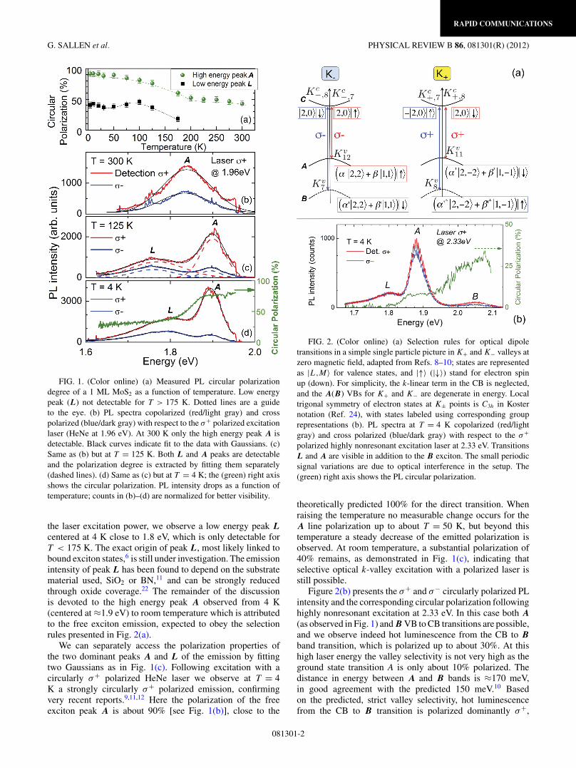
FIG. 1. (Color online) (a) Measured PL circular polarizationdegree of a 1 ML MoS2 as a function of temperature. Low energypeak (L) not detectable for T > 175 K. Dotted lines are a guideto the eye. (b) PL spectra copolarized (red/light gray) and crosspolarized (blue/dark gray) with respect to the σ+ polarized excitationlaser (HeNe at 1.96 eV). At 300 K only the high energy peak A isdetectable. Black curves indicate fit to the data with Gaussians. (c)Same as (b) but at T = 125 K. Both L and A peaks are detectableand the polarization degree is extracted by fitting them separately(dashed lines). (d) Same as (c) but at T = 4 K; the (green) right axisshows the circular polarization. PL intensity drops as a function oftemperature; counts in (b)–(d) are normalized for better visibility.
the laser excitation power, we observe a low energy peak Lcentered at 4 K close to 1.8 eV, which is only detectable forT < 175 K. The exact origin of peak L, most likely linked tobound exciton states,6 is still under investigation. The emissionintensity of peak L has been found to depend on the substratematerial used, SiO2 or BN,11 and can be strongly reducedthrough oxide coverage.22 The remainder of the discussionis devoted to the high energy peak A observed from 4 K(centered at ≈1.9 eV) to room temperature which is attributedto the free exciton emission, expected to obey the selectionrules presented in Fig. 2(a).
We can separately access the polarization properties ofthe two dominant peaks A and L of the emission by fittingtwo Gaussians as in Fig. 1(c). Following excitation with acircularly σ+ polarized HeNe laser we observe at T = 4K a strongly circularly σ+ polarized emission, confirmingvery recent reports.9,11,12 Here the polarization of the freeexciton peak A is about 90% [see Fig. 1(b)], close to the
FIG. 2. (Color online) (a) Selection rules for optical dipoletransitions in a simple single particle picture in K+ and K− valleys atzero magnetic field, adapted from Refs. 8–10; states are representedas |L,M〉 for valence states, and |↑〉 (|↓〉) stand for electron spinup (down). For simplicity, the k-linear term in the CB is neglected,and the A(B) VBs for K+ and K− are degenerate in energy. Localtrigonal symmetry of electron states at K± points is C3h in Kosternotation (Ref. 24), with states labeled using corresponding grouprepresentations (b). PL spectra at T = 4 K copolarized (red/lightgray) and cross polarized (blue/dark gray) with respect to the σ+
polarized highly nonresonant excitation laser at 2.33 eV. TransitionsL and A are visible in addition to the B exciton. The small periodicsignal variations are due to optical interference in the setup. The(green) right axis shows the PL circular polarization.
theoretically predicted 100% for the direct transition. Whenraising the temperature no measurable change occurs for theA line polarization up to about T = 50 K, but beyond thistemperature a steady decrease of the emitted polarization isobserved. At room temperature, a substantial polarization of40% remains, as demonstrated in Fig. 1(c), indicating thatselective optical k-valley excitation with a polarized laser isstill possible.
Figure 2(b) presents the σ+ and σ− circularly polarized PLintensity and the corresponding circular polarization followinghighly nonresonant excitation at 2.33 eV. In this case both A(as observed in Fig. 1) and B VB to CB transitions are possible,and we observe indeed hot luminescence from the CB to Bband transition, which is polarized up to about 30%. At thishigh laser energy the valley selectivity is not very high as theground state transition A is only about 10% polarized. Thedistance in energy between A and B bands is ≈170 meV,in good agreement with the predicted 150 meV.10 Basedon the predicted, strict valley selectivity, hot luminescencefrom the CB to B transition is polarized dominantly σ+,
081301-2
RAPID COMMUNICATIONS
ROBUST OPTICAL EMISSION POLARIZATION IN MoS . . . PHYSICAL REVIEW B 86, 081301(R) (2012)
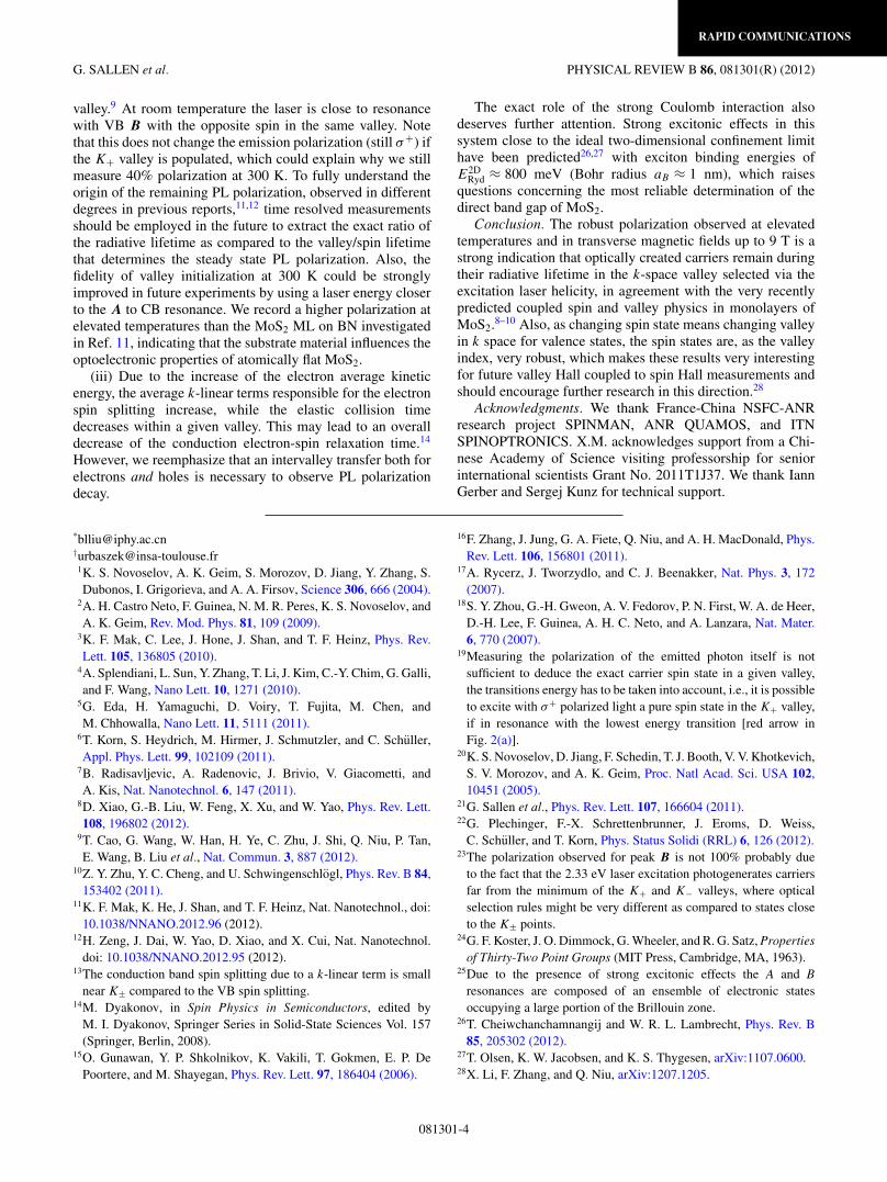
FIG. 3. (Color online) (a) Comparison of PL spectra of a singleMoS2 ML recorded for a transverse magnetic field BT = 0, 4.5, and8.5 T under otherwise identical experimental conditions using HeNelaser at 1.96 eV. Inset: Experimental geometry. (b) Measured PLcircular polarization degree of the PL as a function of the appliedtransverse magnetic field BT for A exciton at T = 4 K (squares) andat T = 100 K (circles).
because the radiative recombination rate is fast comparedto the combined rates of the processes necessary to emitσ− polarized light (i.e., change in k-valley, spin, and orbitalangular momentum).23
A second crucial experimental test for the stability of the op-tically created valley polarization is the application of a trans-verse magnetic field. The spin quantization axis is chosen alongthe light propagation direction, i.e., perpendicular to the MoS2
layer. as indicated in the inset of Fig. 3(a), where the magneticfield BT is applied in the MoS2 plane. In a classical picture forfree carrier spins, the application of a magnetic field perpendic-ular to the spin quantization axis results in a precession of thespin around the applied field. As a result, the spin componentalong the quantization axis measured via the PL polarizationdegree in the circular basis would strongly decrease and even-tually average out to zero in standard Hanle experiments.14
With this simple picture in mind the constant polarizationobserved at T = 4 K in transverse magnetic fields up to 9 Tand at T = 100 K in a field of BT = 6 T shown in Fig. 3(b)seems very surprising. Again one needs to take into accountthe very unusual MoS2 band structure, as discussed below.
Discussion. Both series of experiments detailed in Figs. 1and 3 show robust PL polarization following σ+ polarized laserexcitation, i.e., the processes leading to a change in the valleystate for both conduction and valence carriers and hence σ−polarized emission are not very efficient. The emission is basedon the dipole allowed recombination of a conduction electron
with a valence hole, which we have detailed in Fig. 2(a). Themain contribution to the strong optical absorption, which isreported to be nearly 10%,3–5,11 comes from the Mo d orbitals(characterized by α), taking into account the contribution oftransitions involving states in adjacent cells in k space. β char-acterizes the minute contribution of the p orbitals (L = 1) tothe p-d hybridized VB states. The local trigonal symmetry ofelectron states in monolayer MoS2 at K± points is C3h in Kosternotation,24 and we have accordingly labeled the states usingthe corresponding group representations to which they belong.This leads us to predict the following: (i) The only symmetryallowed coupling introduced by a transverse magnetic field BT
is in principle between VB A and VB B, and between VB Aand CB, all of the same valley. This coupling would not changethe emitted light polarization. In addition, the large energy dif-ference between these bands makes this coupling vanishinglysmall. (ii) BT does not couple states of inequivalent K+ andK− valleys. If the states indeed have the predicted symmetry,even a strong transverse field BT would result in a constantemission polarization when increasing BT . Our results seemto validate this prediction, even at elevated temperatures of100 K in a field of BT = 6 T as shown in Fig. 3(b), in additionto the initial reports in Ref. 12 for small fields.
Note that we do not have a clear spectral signature thatwould allow identifying the exciton charge state as suggestedin Ref. 11. We therefore assume, in accordance with theintriguing polarization properties, the existence of neutralX0 and/or negatively charged excitons X−. The negativelycharged exciton X− consists of two electrons in a singlet stateand an unpaired hole. Measuring the PL polarization allowsmonitoring directly the orientation of the hole spin as electron-hole Coulomb exchange effects essentially cancel out. For theX0, following σ± photon absorption, bright excitons with atotal (pseudo)spin of +1 or −1 are created. Dipole allowedoptical transitions conserve the spin. So if only one of thecarriers (electron or hole) flips, the X0 becomes dark andnonradiative recombination might be favored. An electron spinflip is energetically feasible based on (nearly) degenerate con-duction states. Hole spin flips, at the center of the investigationhere, involve changing valley and are hence far less likely. Toobserve PL polarization change from the recombination of anexciton, both carriers have to be flipped (the exciton spin flipsas a whole).14 Importantly, to observe σ− emission followingoptical excitation with σ+ light involves for both X0 and theX− a hole spin flip by going from valley K+ to K−. In thiscontext, changing the temperature has several consequences:
(i) Phonon assisted intervalley scattering (K+ → K−) canbe activated, since the average occupation number of acousticand optical phonons increases for modes with wave vectorq � |K+ − K−|, thus increasing the probability of intervalleytransfer for both electrons and holes.
(ii) As the temperature is increased, the band gapdecreases,6 but the laser energy in Fig. 1 is kept constantat 1.96 eV, which is very close to resonance with the top VBA to the bottom of the CB direct transition at T < 50 K.In a simple, independent particle picture, when raising thetemperature, carriers increasingly further away from the K+point are optically injected25 and the consistently high PLpolarization observed in Fig. 1(a) indicates that the chiralvalley selectivity is, as predicted, very high throughout the
081301-3
RAPID COMMUNICATIONS
G. SALLEN et al. PHYSICAL REVIEW B 86, 081301(R) (2012)
valley.9 At room temperature the laser is close to resonancewith VB B with the opposite spin in the same valley. Notethat this does not change the emission polarization (still σ+) ifthe K+ valley is populated, which could explain why we stillmeasure 40% polarization at 300 K. To fully understand theorigin of the remaining PL polarization, observed in differentdegrees in previous reports,11,12 time resolved measurementsshould be employed in the future to extract the exact ratio ofthe radiative lifetime as compared to the valley/spin lifetimethat determines the steady state PL polarization. Also, thefidelity of valley initialization at 300 K could be stronglyimproved in future experiments by using a laser energy closerto the A to CB resonance. We record a higher polarization atelevated temperatures than the MoS2 ML on BN investigatedin Ref. 11, indicating that the substrate material influences theoptoelectronic properties of atomically flat MoS2.
(iii) Due to the increase of the electron average kineticenergy, the average k-linear terms responsible for the electronspin splitting increase, while the elastic collision timedecreases within a given valley. This may lead to an overalldecrease of the conduction electron-spin relaxation time.14
However, we reemphasize that an intervalley transfer both forelectrons and holes is necessary to observe PL polarizationdecay.
The exact role of the strong Coulomb interaction alsodeserves further attention. Strong excitonic effects in thissystem close to the ideal two-dimensional confinement limithave been predicted26,27 with exciton binding energies ofE2D
Ryd ≈ 800 meV (Bohr radius aB ≈ 1 nm), which raisesquestions concerning the most reliable determination of thedirect band gap of MoS2.
Conclusion. The robust polarization observed at elevatedtemperatures and in transverse magnetic fields up to 9 T is astrong indication that optically created carriers remain duringtheir radiative lifetime in the k-space valley selected via theexcitation laser helicity, in agreement with the very recentlypredicted coupled spin and valley physics in monolayers ofMoS2.8–10 Also, as changing spin state means changing valleyin k space for valence states, the spin states are, as the valleyindex, very robust, which makes these results very interestingfor future valley Hall coupled to spin Hall measurements andshould encourage further research in this direction.28
Acknowledgments. We thank France-China NSFC-ANRresearch project SPINMAN, ANR QUAMOS, and ITNSPINOPTRONICS. X.M. acknowledges support from a Chi-nese Academy of Science visiting professorship for seniorinternational scientists Grant No. 2011T1J37. We thank IannGerber and Sergej Kunz for technical support.
*[email protected]†[email protected]. S. Novoselov, A. K. Geim, S. Morozov, D. Jiang, Y. Zhang, S.Dubonos, I. Grigorieva, and A. A. Firsov, Science 306, 666 (2004).
2A. H. Castro Neto, F. Guinea, N. M. R. Peres, K. S. Novoselov, andA. K. Geim, Rev. Mod. Phys. 81, 109 (2009).
3K. F. Mak, C. Lee, J. Hone, J. Shan, and T. F. Heinz, Phys. Rev.Lett. 105, 136805 (2010).
4A. Splendiani, L. Sun, Y. Zhang, T. Li, J. Kim, C.-Y. Chim, G. Galli,and F. Wang, Nano Lett. 10, 1271 (2010).
5G. Eda, H. Yamaguchi, D. Voiry, T. Fujita, M. Chen, andM. Chhowalla, Nano Lett. 11, 5111 (2011).
6T. Korn, S. Heydrich, M. Hirmer, J. Schmutzler, and C. Schuller,Appl. Phys. Lett. 99, 102109 (2011).
7B. Radisavljevic, A. Radenovic, J. Brivio, V. Giacometti, andA. Kis, Nat. Nanotechnol. 6, 147 (2011).
8D. Xiao, G.-B. Liu, W. Feng, X. Xu, and W. Yao, Phys. Rev. Lett.108, 196802 (2012).
9T. Cao, G. Wang, W. Han, H. Ye, C. Zhu, J. Shi, Q. Niu, P. Tan,E. Wang, B. Liu et al., Nat. Commun. 3, 887 (2012).
10Z. Y. Zhu, Y. C. Cheng, and U. Schwingenschlogl, Phys. Rev. B 84,153402 (2011).
11K. F. Mak, K. He, J. Shan, and T. F. Heinz, Nat. Nanotechnol., doi:10.1038/NNANO.2012.96 (2012).
12H. Zeng, J. Dai, W. Yao, D. Xiao, and X. Cui, Nat. Nanotechnol.doi: 10.1038/NNANO.2012.95 (2012).
13The conduction band spin splitting due to a k-linear term is smallnear K± compared to the VB spin splitting.
14M. Dyakonov, in Spin Physics in Semiconductors, edited byM. I. Dyakonov, Springer Series in Solid-State Sciences Vol. 157(Springer, Berlin, 2008).
15O. Gunawan, Y. P. Shkolnikov, K. Vakili, T. Gokmen, E. P. DePoortere, and M. Shayegan, Phys. Rev. Lett. 97, 186404 (2006).
16F. Zhang, J. Jung, G. A. Fiete, Q. Niu, and A. H. MacDonald, Phys.Rev. Lett. 106, 156801 (2011).
17A. Rycerz, J. Tworzydlo, and C. J. Beenakker, Nat. Phys. 3, 172(2007).
18S. Y. Zhou, G.-H. Gweon, A. V. Fedorov, P. N. First, W. A. de Heer,D.-H. Lee, F. Guinea, A. H. C. Neto, and A. Lanzara, Nat. Mater.6, 770 (2007).
19Measuring the polarization of the emitted photon itself is notsufficient to deduce the exact carrier spin state in a given valley,the transitions energy has to be taken into account, i.e., it is possibleto excite with σ+ polarized light a pure spin state in the K+ valley,if in resonance with the lowest energy transition [red arrow inFig. 2(a)].
20K. S. Novoselov, D. Jiang, F. Schedin, T. J. Booth, V. V. Khotkevich,S. V. Morozov, and A. K. Geim, Proc. Natl Acad. Sci. USA 102,10451 (2005).
21G. Sallen et al., Phys. Rev. Lett. 107, 166604 (2011).22G. Plechinger, F.-X. Schrettenbrunner, J. Eroms, D. Weiss,
C. Schuller, and T. Korn, Phys. Status Solidi (RRL) 6, 126 (2012).23The polarization observed for peak B is not 100% probably due
to the fact that the 2.33 eV laser excitation photogenerates carriersfar from the minimum of the K+ and K− valleys, where opticalselection rules might be very different as compared to states closeto the K± points.
24G. F. Koster, J. O. Dimmock, G. Wheeler, and R. G. Satz, Propertiesof Thirty-Two Point Groups (MIT Press, Cambridge, MA, 1963).
25Due to the presence of strong excitonic effects the A and Bresonances are composed of an ensemble of electronic statesoccupying a large portion of the Brillouin zone.
26T. Cheiwchanchamnangij and W. R. L. Lambrecht, Phys. Rev. B85, 205302 (2012).
27T. Olsen, K. W. Jacobsen, and K. S. Thygesen, arXiv:1107.0600.28X. Li, F. Zhang, and Q. Niu, arXiv:1207.1205.
081301-4


![TASK ORDER · Web viewThe emission and removal estimates produced in the greenhouse gas inventory by [coordinating/lead agency issuing RFP/ToR] represents a robust data analysis and](https://img.pdfslide.net/doc/110x75/60cf5951f983af5977473643/task-order-web-view-the-emission-and-removal-estimates-produced-in-the-greenhouse.jpg)


![Robust Model Predictive Control - Carnegie Mellon …cepac.cheme.cmu.edu/.../Ronust_Control_Classnotes.pdf1 Robust Model Predictive Control Formulations of robust control [1] The robust](https://img.pdfslide.net/doc/110x75/5aab45707f8b9a2b4c8bd345/robust-model-predictive-control-carnegie-mellon-cepacchemecmueduronustcontrol.jpg)
![Robust automated computational approach for classifying …facundomanes.com/wp-content/uploads/2019/09/Donnelly-et... · 2019-09-03 · imaging [MRI] and positron emission tomography](https://img.pdfslide.net/doc/110x75/5ed5cc0e36d96224827ed3cd/robust-automated-computational-approach-for-classifying-2019-09-03-imaging-mri.jpg)